 | –≠–ª–µ–∫—Ç—Ä–æ–Ω–Ω—ã–π –∫–æ–º–ø–æ–Ω–µ–Ω—Ç: MT8963AE1 | –°–∫–∞—á–∞—Ç—å:  PDF PDF  ZIP ZIP |
Document Outline
- Features
- Figure 1 - Functional Block Diagram
- Description
- Figure 2 - Pin Connections
- Pin Description
- Figure 3 - m-Law Encoder Transfer Characteristic
- Figure 4 - A-Law Encoder Transfer Characteristic
- Functional Description
- Transmit Path
- Receive Path
- VRef
- Figure 5 - Typical Voltage Reference Circuit
- Timing
- Digital Control Functions
- Mode 1
- Mode 2
- Mode 3
- Table 1 - Digital Control Modes
- Table 2 - Control States - Register A
- Control Registers A, B
- Chip Testing
- Loopback
- Logic Control Outputs SD0-5
- Figure 6 - Typical Line Termination
- Table 3 - Control States - Register B
- Powerdown
- Figure 7 - Typical Use of the Special Drive Outputs
- Figure 8 - Example Architecture of a Simple Digital Switching System using the MT8960-67
- Absolute Maximum Ratings*
- Recommended Operating Conditions - Voltages are with respect to GNDD unless otherwise stated
- DC Electrical Characteristics - Voltages are with respect to GNDD unless otherwise stated.
- TA=0 to 70∞C, VDD=5V±5%, VEE=-5V±5%, VRef=2.5V±0.5%, GNDA=GNDD=0V,Clock Frequency =2.048MHz. Outp...
- AC Electrical Characteristics - Voltages are with respect to GNDD unless otherwise stated.
- TA=0 to 70∞C, VDD=5V±5%, VEE=-5V±5%, VRef=2.5V±0.5%, GNDA=GNDD=0V, Clock Frequency=2.048 MHz. Out...
- AC Electrical Characteristics - Transmit (A/D) Path - Voltages are with respect to GNDD unless ot...
- TA=0 to 70∞C, VDD=5V±5%, VEE=-5V±5%, VRef=2.5V±0.5%, GNDA=GNDD=0V, Clock Frequency = 2.048MHz,
- Filter Gain Setting = 0dB. Outputs unloaded unless otherwise specified.
- AC Electrical Characteristics - Receive (D/A) Path - Voltages are with respect to GNDD unless oth...
- TA=0 to 70∞C, VDD=5V±5%, VEE=-5V±5%, VRef=2.5V±0.5%, GNDA=GNDD=0V, Clock Frequency = 2.048MHz,
- Filter Gain Setting = 0dB. Outputs unloaded unless otherwise specified.
- Figure 10 - Attenuation vs Frequency for Transmit (A/D) Filter
- Figure 11 - Attenuation vs Frequency for Receive (D/A) Filter
- Figure 12 - Variation of Gain With Input Level
- Figure 13 - Signal to Total Distortion Ratio vs Input Level
- Figure 14 - Envelope Delay Variation Frequency
- Figure 15 - Overload Distortion (End-to-End)
1
Zarlink Semiconductor Inc.
Zarlink, ZL and the Zarlink Semiconductor logo are trademarks of Zarlink Semiconductor Inc.
Copyright 2003-2005, Zarlink Semiconductor Inc. All Rights Reserved.
Features
∑ ST-BUS
compatible
∑ Transmit/Receive filters & PCM Codec in one I.C
∑ Meets AT&T D3/D4 and CCITT G711 and G712
∑
µ-Law: MT8960/62/64/67
∑ A-Law: MT8961/63/65/67
∑ Low power consumption:
Op.: 30 mW typ.
Stby.: 2.5 mW typ.
∑ Digital Coding Options:
MT8964/65/66/67 CCITT Code
MT8960/61/62/63 Alternative Code
∑ Digitally controlled gain adjust of both filters
∑ Analog and digital loopback
∑ Filters and codec independently user accessible
for testing
∑ Powerdown mode available
∑ 2.048 MHz master clock input
∑ Up to six uncommitted control outputs
∑
±5 V ±5% power supply
Description
Manufactured in ISO
2
-CMOS, these integrated
filter/codecs are designed to meet the demanding
performance needs of the digital telecommunications
industry, e.g., PABX, Central Office, Digital telephones.
February 2005
Ordering Information
MT8960/61/64/65AE
18 Pin PDIP
Tubes
MT8962/63AE
20 Pin PDIP
Tubes
MT8962/63/66/67AS
20 Pin SOIC
Tubes
MT8963ASR
20 Pin SOIC
Tape & Reel
MT8960AE1
18 Pin PDIP*
Tubes
MT8962/63AE1
20 Pin PDIP*
Tubes
MT8962AS1
20 Pin SOIC*
Tubes
MT8963AS1
20 Pin SOIC*
Tubes
*Pb Free Matte Tin
-40
∞C to +85∞C
ISO
2
-CMOS
MT8960/61/62/63/64/65/66/67
Integrated PCM Filter Codec
Data Sheet
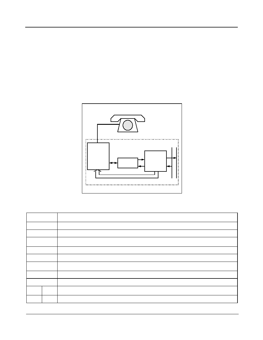
Figure 1 - Functional Block Diagram
ANUL
V
X
SD0
SD1
SD2
SD3
SD4
SD5
V
R
V
Ref
GNDA GNDD V
DD
V
EE
DSTo
CSTi
CA
F1i
C2i
DSTi
Transmit
Filter
Output
Register
Receive
Filter
Analog to
Digital PCM
Encoder
PCM Digital
to Analog
Decoder
Output
Register
Input
Register
A Register
8-Bits
B-Register
8-Bits
Control
Logic

MT8960/61/62/63/64/65/66/67
Data Sheet
2
Zarlink Semiconductor Inc.
Figure 2 - Pin Connections
Pin Description
Pin Name
Description
CSTi
Control ST-BUS In is a TTL-compatible digital input used to control the function of the filter/codec.
Three modes of operation may be effected by applying to this input a logic high (V
DD
), logic low
(GNDD), or an 8-bit serial word, depending on the logic states of CA and F1i.
Functions controlled are: powerdown, filter gain adjust, loopback, chip testing, SD outputs.
DSTi
Data ST-BUS In accepts the incoming 8-bit PCM word. Input is TTL-compatible.
C2i
Clock Input is a TTL-compatible 2.048 MHz clock.
DSTo
Data ST-BUS Out is a three-state digital output driving the PCM bus with the outgoing 8-bit PCM
word.
V
DD
Positive power Supply (+5 V).
F1i
Synchronization Input
is an active low digital input enabling (in conjunction with CA) the PCM input,
PCM output and digital control input. It is internally sampled on every positive edge of the clock, C2i,
and provides frame and channel synchronization.
CA
Control Address is a three-level digital input which enables PCM input and output and determines
into which control register (A or B) the serial data, presented to CSTi, is stored.
SD3
System Drive Output is an open drain output of an N-channel transistor which has its source tied to
GNDA. Inactive state is open circuit.
SD4-5
System Drive Outputs
are
open drain outputs of N-channel transistors which have their source tied
to GNDD. Inactive state is open circuit.
SD0-2
System Drive Outputs
are
"Totempole" CMOS outputs switching between GNDD and V
DD
. Inactive
state is logic low.
V
EE
Negative power supply (-5 V).
V
X
Voice Transmit
is the
analog input to the transmit filter.
ANUL
Auto Null
is used to integrate an internal auto-null signal.
A 0.1
µF capacitor must be connected
between this pin and GNDA.
V
R
Voice Receive
is the
analog output of the receive filter.
GNDA
Analog ground (0 V).
V
Ref
Voltage Reference input to D to A converter.
GNDD
Digital ground (0 V).
1
2
3
4
5
6
7
8
9
10
11
12
20
19
18
17
16
15
14
13
20 PIN PDIP/SOIC
CSTi
DSTi
C2i
DSTo
VDD
SD5
SD4
F1i
CA
SD3
GNDD
VRef
GNDA
VR
ANUL
VX
VEE
SD0
SD1
SD2
1
2
3
4
5
6
7
8
9
10
18
17
16
15
14
13
12
11
18 PIN PDIP
CSTi
DSTi
C2i
DSTo
VDD
F1i
CA
SD3
SD2
GNDD
VRef
GNDA
VR
ANUL
VX
VEE
SD0
SD1
MT8960/61/64/65
MT8962/63/66/67

MT8960/61/62/63/64/65/66/67
Data Sheet
3
Zarlink Semiconductor Inc.
Figure 3 -
µ-Law Encoder Transfer Characteristic
11111111
11110000
11100000
11010000
11000000
10110000
10100000
10010000
10000000
00000000
00010000
00100000
00110000
01000000
01010000
01100000
01110000
01111111
10000000
10001111
10011111
10101111
10111111
11001111
11011111
11101111
11111111
01111111
01101111
01011111
01001111
00111111
00101111
00011111
00001111
00000000
-2.415V -1.207V
0V
+1.207V +2.415V
Bit 7... 0
MSB LSB
Analog Input Voltage (V
IN
)
MT8960/62
Digital Output
MT8964/66
Digital Output
MT8960/61/62/63/64/65/66/67
Data Sheet
4
Zarlink Semiconductor Inc.
Figure 4 - A-Law Encoder Transfer Characteristic
Functional Description
Figure 1 shows the functional block diagram of the MT8960-67. These devices provide the conversion interface
between the voiceband analog signals of a telephone subscriber loop and the digital signals required in a digital
PCM (pulse code modulation) switching system. Analog (voiceband) signals in the transmit path enter the chip at
V
X
, are sampled at 8 kHz, and the samples quantized and assigned 8-bit digital values defined by logarithmic PCM
encoding laws. Analog signals in the receive path leave the chip at V
R
after reconstruction from digital 8-bit words.
Separate switched capacitor filter sections are used for bandlimiting prior to digital encoding in the transmit path
and after digital decoding in the receive path. All filter clocks are derived from the 2.048 MHz master clock input,
C2i. Chip size is minimized by the use of common circuitry performing the A to D and D to A conversion. A
successive approximation technique is used with capacitor arrays to define the 16 steps and 8 chords in the signal
conversion process. Eight-bit PCM encoded digital data enters and leaves the chip serially on DSTi and DSTo
pins, respectively.
Transmit Path
Analog signals at the input (Vx) are firstly bandlimited to 508 kHz by an RC lowpass filter section. This performs the
necessary anti-aliasing for the following first-order sampled data lowpass pre-filter which is clocked at 512 kHz.
This further bandlimits the signal to 124 kHz before a fifth-order elliptic lowpass filter, clocked at 128 kHz, provides
the 3.4 kHz bandwidth required by the encoder section. A 50/60 Hz third-order highpass notch filter clocked at
8 kHz completes the transmit filter path. Accumulated DC offset is cancelled in this last section by a switched-
capacitor auto-zero loop which integrates the sign bit of the encoded PCM word, fed back from the codec and
11111111
11110000
11100000
11010000
11000000
10110000
10100000
10010000
10000000
00000000
00010000
00100000
00110000
01000000
01010000
01100000
01110000
01111111
10101010
10100101
10110101
10000101
10010101
11100101
11110101
11000101
11010101
01010101
01000101
01110101
01100101
00010101
00000101
00110101
00100101
00101010
-2.5V
-1.25V
0V
+1.25V
+2.5V
Bit 7... 0
MSB LSB
Analog Input Voltage (V
IN
)
MT8961/63
Digital Output
MT8965/67
Digital Output

MT8960/61/62/63/64/65/66/67
Data Sheet
5
Zarlink Semiconductor Inc.
injects this voltage level into the non-inverting input of the comparator. An integrating capacitor (of value between
0.1 and 1
µF) must be externally connected from this point (ANUL) to the Analog Ground (GNDA).
The absolute gain of the transmit filter (nominally 0 dB at 1 kHz) can be adjusted from 0 dB to 7 dB in 1 dB steps by
means of three binary controlled gain pads.
The resulting bandpass characteristics with the limits shown in Figure 10 meet the CCITT and AT&T recommended
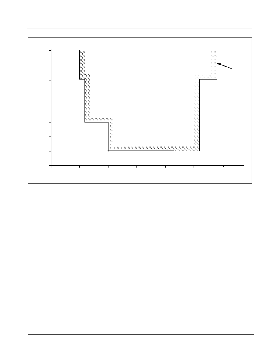
specifications. Typical attenuations are 30 dB for 0-60 Hz and 35 dB for 4.6 kHz and above.
The filter output signal is an 8 kHz staircase waveform which is fed into the codec capacitor array, or alternatively,
into an external capacitive load of 250 pF when the chip is in the test mode. The digital encoder generates an eight-
bit digital word representation of the 8 kHz sampled analog signal. The first bit of serial data stream is bit 7 (MSB)
and represents the sign of the analog signal. Bits 4-6 represent the chord which contains the analog sample value.
Bits 0-3 represent the step value of the analog sample within the selected chord. The MT8960-63 provide a sign
plus magnitude PCM output code format. The MT8964/66 PCM output code conforms to the AT &T D3
specification, i.e., true sign bit and inverted magnitude bits. The MT8965/67 PCM output code conforms to the
CCITT specifications with alternate digit inversion (even bits inverted). See Figs. 3 and 4 for the digital output code
corresponding to the analog voltage, V
IN
, at V
X
input.
The eight-bit digital word is output at DSTo at a nominal rate of 2.048 MHz, via the output buffer as the first 8-bits of
the 125
µs sampling frame.
Receive Path
An eight-bit PCM encoded digital word is received on DSTi input once during the 125
µs period and is loaded into
the input register. A charge proportional to the received PCM word appears on the capacitor array and an 8 kHz
sample and hold circuit integrates this charge and holds it for the rest of the sampling period.
The receive (D/A) filter provides interpolation filtering on the 8 kHz sample and hold signal from the codec. The filter
consists of a 3.4 kHz lowpass fifth-order elliptic section clocked at 128 kHz and performs bandlimiting and
smoothing of the 8 kHz "staircase" waveform. In addition, sinx/x gain correction is applied to the signal to
compensate for the attenuation of higher frequencies caused by the capacitive sample and hold circuit. The
absolute gain of the receive filter can be adjusted from 0 dB to -7 dB in 1 dB steps by means of three binary
controlled gain pads. The resulting lowpass characteristics, with the limits shown in Figure 11, meet the CCITT and
AT & T recommended specifications.
Typical attenuation at 4.6 kHz and above is 30 dB. The filter is followed by a buffer amplifier which will drive 5V
peak/peak into a 10k ohm load, suitable for driving electronic 2-4 wire circuits.
V
Ref
An external voltage must be supplied to the V
Ref
pin which provides the reference voltage for the digital encoding
and decoding of the analog signal. For V
Ref
= 2.5 V, the digital encode decision value for overload (maximum
analog signal detect level) is equal to an analog input V
IN
= 2.415 V (
µ-Law version) or 2.5 V (A-Law version) and is
equivalent to a signal level of 3.17 dBm0 or 3.14 dBm0 respectively, at the codec.
The analog output voltage from the decoder at V
R
is defined as:
µ-Law:
-0.5
2
C
16.5 + S
V
Ref
X
[(
128
)
+
(
128
)(
33
)]
±V
OFFSET
A-Law:
2
C+1
0.5 + S
V
Ref
X
[(
128
)(
32
)]
±V
OFFSET
C=0
MT8960/61/62/63/64/65/66/67
Data Sheet
6
Zarlink Semiconductor Inc.
2
C
16.5 + S
V
Ref
X
[(
128
)(
32
)]
±V
OFFSET
C
0
where C = chord number (0-7)
S = step number (0-15)
V
Ref
is a high impedance input with a varying capacitive load of up to 40 pF.
The recommended reference voltage for the MT8960 series of codecs is 2.5 V
±0.5%. The output voltage from the
reference source should have a maximum temperature coefficient of 100 ppm/C
∞. This voltage should have a total
regulation tolerance of
±0.5% both for changes in the input voltage and output loading of the voltage reference
source. A voltage reference circuit capable of meeting these specifications is shown in Figure 5. Analog
Devices'AD1403A voltage reference circuit is capable of driving a large number of codecs due to the high input
impedance of the V
Ref
input. Normal precautions should be taken in PCB layout design to minimize noise coupling
to this pin. A 0.1
µF capacitor connected from V
Ref
to ground and located as close as possible to the codec is
recommended to minimize noise entering through V
Ref
. This capacitor should have good high frequency
characteristics.
Figure 5 - Typical Voltage Reference Circuit
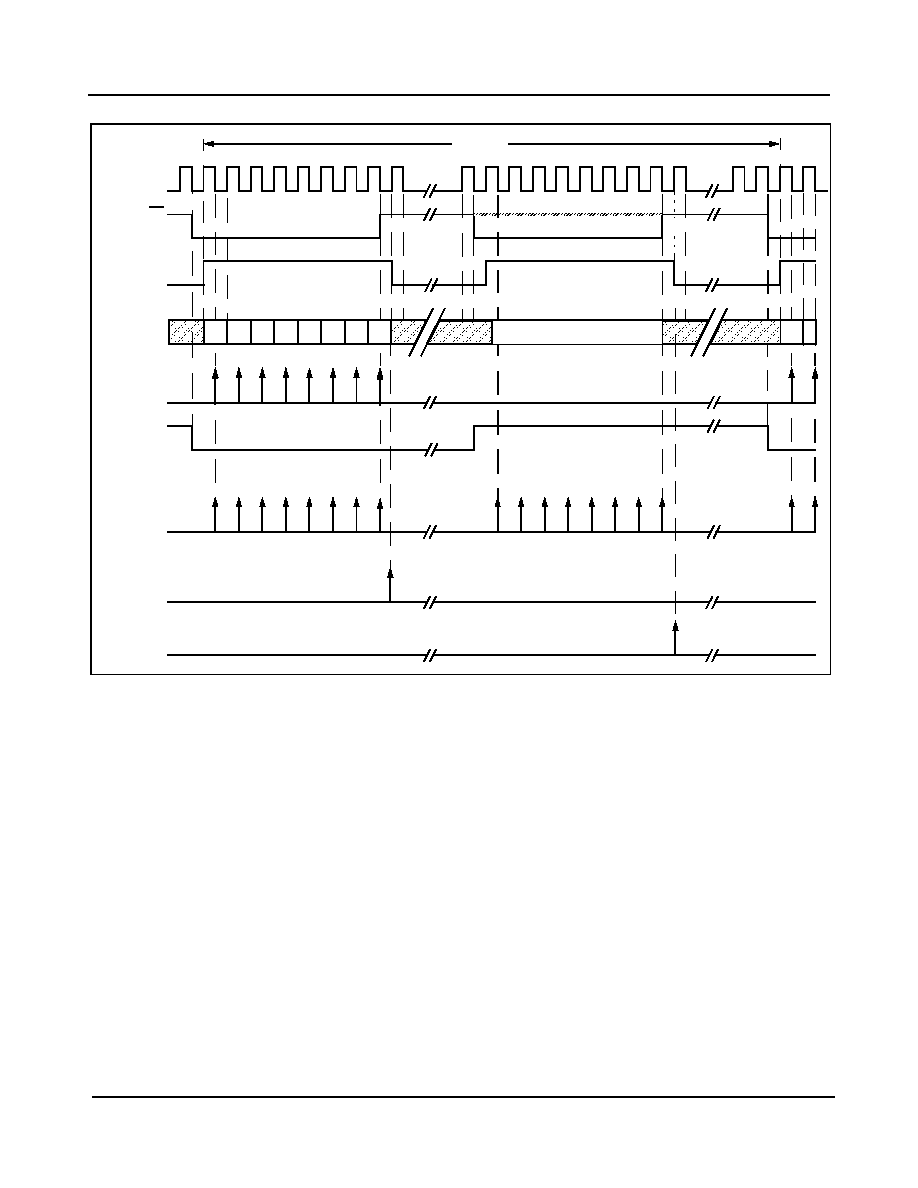
Timing
The codec operates in a synchronous manner (see Figure 9a). The codec is activated on the first positive
edge of
C2i after F1i has gone low. The digital output at DSTo (which is a three-state output driver) will then change from
a high impedance state to the sign bit of the encoded PCM word to be output. This will remain valid until the next
positive edge, when the next most significant bit will be output.
On the first negative clock edge (after F1i signal has been internally synchronized and CA is at GNDD or V
EE
) the
logic signal present at DSTi will be clocked into the input shift register as the sign bit of the incoming PCM word.
The eight-bit word is thus input at DSTi on negative edges of C2i and output at DSTo on positive edges of C2i.
F1i must return to a high level after the eighth clock pulse causing DSTo to enter high impedance and
preventing further input data to DSTi. F1i will continue to be sampled on every positive edge of C2i. (Note: F1i may
subsequently be taken low during the same sampling frame to enable entry of serial data into CSTi. This occurs
usually mid-frame, in conjunction with CA=V
DD
, in order to enter an 8-bit control word into Register B. In this case,
PCM input and output are inhibited by CA at V
DD
.)
Internally the codec will then perform a decode cycle on the newly input PCM word. The sampled and held analog
signal thus decoded will be updated 25
µs from the start of the cycle. After this the analog input from the filter is
sampled for 18
µs, after which digital conversion takes place during the remaining 82 µs of the sampling cycle.
NC
1
2
3
4
5
6
7
8
AD1403A
+5 V
2.5 V
0.1
µF
V
Ref
MT8960-67
FILTER/CODEC
NC
NC
NC
NC

MT8960/61/62/63/64/65/66/67
Data Sheet
7
Zarlink Semiconductor Inc.
Since a single clock frequency of 2.048 MHz is required, all digital data is input and output at this rate. DSTo,
therefore, assumes a high impedance state for all but 3.9
µs of the 125 µs frame. Similarly, DSTi input data is valid
for only 3.9
µs.
Digital Control Functions
CSTi is a digital input (levels GNDD to V
DD
) which is used to control the function of the filter/codec. It operates in
three different modes depending on the logic levels applied to the Control Address input (CA) and chip enable input
(F1i) (see Table 1).
Mode 1
CA=-5V (V
EE
); CSTi=0V (GNDD)
The filter/codec is in normal operation with nominal transmit and receive gain of 0dB. The SD outputs are in their
active states and the test modes cannot be entered.
CA = -5V (V
EE
); CSTi = +5V (V
DD
)
A state of powerdown is forced upon the chip whereby DSTo
becomes high impedance, V
R
is connected to GNDA
and all analog sections have power removed.
Mode 2
CA= -5V (V
EE
); CSTi receives an eight-bit control word
CSTi accepts a serial data stream synchronously with DSTi (i.e., it accepts an eight-bit serial word in a 3.9
µs
timeslot, updated every 125
µs, and is specified identically to DSTi for timing considerations). This eight-bit control
word is entered into Control Register A and enables programming of the following functions: transmit and receive
gain, powerdown, loopback. Register B is reset to zero and the SD outputs assume their inactive state. Test modes
cannot be entered.
Mode 3
CA=0V (GNDD); CSTi receives an eight-bit control word
As in Mode 2, the control word enters Register A and the aforementioned functions are controlled. In this mode,
however, Register B is not reset, thus not affecting the states of the SD outputs.
CA=+5V (V
DD
); CSTi receives an 8-bit control word
In this case the control word is transferred into Register B. Register A is unaffected. The input and output of PCM
data is inhibited.
The contents of Register B controls the six uncommitted outputs SD0-SD5 (four outputs, SD0-SD3, on
MT8960/61/64/65 versions of chip) and also provide entry into one of the three test modes of the chip.
Note: For Modes 1 and 2, F1i must be at logic low for one period of 3.9
µs, in each 125 µs cycle, when PCM data
is being input and output, and the control word at CSTi enters Register A. For Mode 3, F1i must be at a logic low for
two periods of 3.9
µs, in each 125 µs cycle. In the first period, CA must be at GNDD or V
EE
, and in the second
period CA must be high (V
DD)
.
MT8960/61/62/63/64/65/66/67
Data Sheet
8
Zarlink Semiconductor Inc.
Table 1 - Digital Control Modes
Mode
CA
CSTi
Function
1
(Note 1)
V
EE
GNDD
Normal chip operation.
V
DD
Powerdown.
2
V
EE
Serial
Eight-bit control word into Register A. Register B is reset.
Data
3
(Note 2)
GNDD
Serial
Eight-bit control word into register A. Register B is unaffected.
Data
V
DD
Serial
Eight-bit control word into register A. Register B is unaffected.
Data
Note 1:
When operating in Mode 1, there should be only one frame pulse (F1i) per 125
µs frame
Note 2:
When operating in Mode 3, PCM input and output is inhibited by CA=V
DD
.
BIT 2
BIT 1
BIT 0
TRANSMIT (A/D)
FILTER GAIN (dB)
0
0
0
0
0
0
1
+ 1
0
1
0
+ 2
0
1
1
+ 3
1
0
0
+ 4
1
0
1
+ 5
1
1
0
+ 6
1
1
1
+ 7
BIT 5
BIT 4
BIT 3
RECEIVE (D/A)
FILTER GAIN (dB)
0
0
0
0
0
0
1
- 1
0
1
0
- 2
0
1
1
- 3
1
0
0
- 4
1
0
1
- 5
1
1
0
- 6
1
1
1
- 7

MT8960/61/62/63/64/65/66/67
Data Sheet
9
Zarlink Semiconductor Inc.
Table 2 - Control States - Register A
Control Registers A, B
The contents of these registers control the filter/codec functions as described in Tables 2 and 3.
Bit 7 of the registers is the MSB and is defined as the first bit of the serial data stream input (corresponding to the
sign bit of the PCM word).
On initial power-up these registers are set to the powerdown condition for a maximum of 25 clock cycles. During
this time it is impossible to change the data in these registers.
Chip Testing
By enabling Register B with valid data (eight-bit control word input to CSTi when F1i=GNDD and CA= V
CC
) the chip
testing mode can be entered. Bits 6 and 7 (most sign bits) define states for testing the transmit filter, receive filter
and the codec function. The input in each case is V
X
input and the output in each case is V
R
output. (See Table 3 for
details.)
Loopback
Loopback of the filter/codec is controlled by the control word entered into Register A. Bits 6 and 7 (most sign bits)
provide either a digital or analog loopback condition. Digital loopback is defined as follows:
∑ PCM input data at DSTi is latched into the PCM input register and the output of this register is connected to
the input of the 3-state PCM output register.
∑ The digital input to the PCM digital-to-analog decoder is disconnected, forced to zero (0).
∑ The output of the PCM encoder is disabled and thus the encoded data is lost. The PCM output at DSTo is
determined by the PCM input data.
Analog loopback is defined as follows:
∑ PCM input data is latched, decoded and filtered as normal but not output at V
R
.
∑ Analog output buffer at V
R
has its input shorted to GNDA and disconnected from the receive filter output.
∑ Analog input at V
X
is disconnected from the transmit filter input.
∑ The receive filter output is connected to the transmit filter input. Thus the decode signal is fed back through
the receive path and encoded in the normal way. The analog output buffer at V
R
is not tested by this
configuration.
In both cases of loopback, DSTi is the input and DSTo is the output.
BIT 7
BIT 6
FUNCTION CONTROL
0
0
Normal operation
0
1
Digital Loopback
1
0
Analog Loopback
1
1
Powerdown
BIT 2
BIT 1
BIT 0
TRANSMIT (A/D)
FILTER GAIN (dB)
MT8960/61/62/63/64/65/66/67
Data Sheet
10
Zarlink Semiconductor Inc.
Logic Control Outputs SD0-5
These outputs are directly controlled by the logic states of bits 0-5 in Register B. A logic low (GNDD) in Register B
causes the SD outputs to assume an inactive state. A logic high (V
DD
) in Register B causes the SD outputs to
assume an active state (see Table 3). SD0-2
switch between GNDD and V
DD
and may be used to control
external logic or transistor circuitry, for example, that employed on the line card for performing such functions
as relay drive for application of ringing to line, message waiting indication, etc.
SD3-5
are used primarily to drive external analog circuitry. Examples may include the switching in or out of gain
sections or filter sections (e.g., ring trip filter) (Figure 7).
MT8962/63/66/67 provides all six SD outputs.
MT8960/61/64/65 each packaged in an 18-pin DIP provide only four control outputs, SD0-3.
Figure 6 - Typical Line Termination
BITS 0-2
LOGIC CONTROL OUTPUTS SD
0
-SD
2
0
Inactive state - logic low (GNDD).
1
Active state - logic high (V
DD
).
BIT 3
LOGIC CONTROL OUTPUT SD
3
0
Inactive state - High Impedance.
1
Active state - GNDA.
BITS 4,5
LOGIC CONTROL OUTPUTS SD
4
, SD
5
0
Inactive state - High Impedance.
1
Active state - GNDD.
BIT 7
BIT 6
CHIP TESTING CONTROLS
0
0
Normal operation.
Telephone Set
2 Wire
Analog
Supervision
Protection
Battery
Feed
Ringing
PCM Highway
2W/4W
Converter
MT8960/61
MT8962/63
MT8964/65
MT8966/67

MT8960/61/62/63/64/65/66/67
Data Sheet
11
Zarlink Semiconductor Inc.
Table 3 - Control States - Register B
Powerdown
Powerdown of the chip is achieved in several ways:
Internal Control:
1)
Initial Power-up. Initial application of V
DD
and V
EE
causes powerdown for a period of 25 clock cycles and
during this period the chip will accept input only from C2i. The B-register is reset to zero forcing SD0-5 to
be inactive. Bits 0-5 of Register A (gain adjust bits) are forced to zero and bits 6 and 7 of Register A
become logic high thus reinforcing the powerdown.
2)
Loss of C2i. Powerdown is entered 10 to 40
µs after C2i has assumed a continuous logic high (V
DD
). In
this condition the chip will be in the same state as in (1) above.
Note: If C2i stops at a continuous logic low (GNDD), the digital data and status is indeterminate.
External Control:
1)
Register A. Powerdown is controlled by bits 6 and 7 (when both at logic high) of Register A which in turn
receives its control word input via CSTi, when F1i is low and CA input is either at V
EE
or GNDD. Power is
removed from the filters and analog sections of the chip. The analog output buffer at V
R
will be connected
to GNDA. DSTo becomes high impedance and the clocks to the majority of the logic are stopped. SD
outputs are unaffected and may be updated as normal.
2)
CSTi
Input. With CA at V
EE
and CSTi held at continuous logic high the chip assumes the same state as
described in External Control (1) above.
0
1
Transmit filter testing, i.e.:
Transmit filter input connected to V
X
input
Receive filter and Buffer disconnected from V
R
1
0
Receive filter testing, i.e.:
Receive filter input connected to V
X
input
Receive filter input disconnected from codec
1
1
Codec testing i.e.:
Codec analog input connected to V
X
Codec analog input disconnected from transmit filter output
Codec analog output connected to V
R
V
R
disconnected from receive filter output
BITS 0-2
LOGIC CONTROL OUTPUTS SD
0
-SD
2

MT8960/61/62/63/64/65/66/67
Data Sheet
12
Zarlink Semiconductor Inc.
Figure 7 - Typical Use of the Special Drive Outputs
From ST-BUS
From ST-BUS
Master Clock
to ST-BUS
5 V
Alignment
Register Select
CSTi
DSTi
C2i
DSTo
V
DD
F1i
CA
SD3
SD2
GNDD
V
Ref
GNDA
V
R
ANUL
V
X
V
EE
SD0
SD1
2.5 V
0.1
µF
-5 V
MT8960/61/64/65
Gain
Section
2/4 Wire
Converter
Message
Waiting
(With Relay
Drive)
Ring Feed
(With Relay
Drive)
-100 V DC
Telephone
Line
-48 V DC
-48 V DC
90 V
RMS
Ring Trip
Filter
(With Relay
Drive)

MT8960/61/62/63/64/65/66/67
Data Sheet
13
Zarlink Semiconductor Inc.
Figure 8 - Example Architecture of a Simple Digital Switching System using the MT8960-67
DSTi
DSTo
CDTi
V
X
V
R
SD0
SDn
.
.
.
∑
∑
∑
Repeated for Lines
2 to 255
Line 1
Line 256
8
8
8
8
Speech
Switch
-
8980
Controlling
Micro-
Processor
Control &
Signalling
-
8980
DSTi
DSTo
CDTi
V
X
V
R
SD0
SDn
.
.
.
∑
∑
∑
∑
∑
∑
Repeated for Lines
2 to 255
Line
Interface
&
Monitoring
Circuitry
Line
Interface
&
Monitoring
Circuitry
∑
∑
∑
MT8960-67
MT8960-67

MT8960/61/62/63/64/65/66/67
Data Sheet
14
Zarlink Semiconductor Inc.
* Exceeding these values may cause permanent damage. Functional operation under these conditions is not implied.
Note 1: Temperature coefficient of V
Ref
should be better than 100 ppm/
∞
C.
Absolute Maximum Ratings*
Parameter
Symbol
Min.
Max.
Units
1
DC Supply Voltages
V
DD
-GNDD
-0.3
+6.0
V
V
EE
-GNDD
-6.0
+0.3
V
2
Reference Voltage
V
Ref
GNDA
V
DD
V
3
Analog Input
V
X
V
EE
V
DD
V
4
Digital Inputs
Except CA
GNDD-0.3
V
DD
+0.3
V
CA
V
EE
-0.3
V
DD
+0.3
V
5
Output Voltage
SD
0-2
GNDD-0.3
V
DD
+0.3
V
SD
3
V
EE
-0.3
V
DD
+0.3
V
SD
4-5
V
EE
-0.3
V
DD
+0.3
V
6
Current On Any Pin
I
I
20
mA
7
Storage Temperature
T
S
-55
+125
∞C
8
Power Dissipation at 25
∞C
(Derate 16 mW/
∞
C above 75
∞
C)
P
Diss
500
mW
Recommended Operating Conditions -
Voltages are with respect to GNDD unless otherwise stated
Characteristics
Sym.
Min.
Typ.*
Max.
Units
Comments
1
Supply Voltage
V
DD
4.75
5.0
5.25
V
V
EE
-5.25
-5.0
-4.75
V
V
Ref
2.5
V
See Note 1
2
Voltage On Digital Ground
VGNDD
-0.1
0.0
+0.1
Vdc
Ref. to GNDA
-0.4
0.0
+0.4
Vac
Ref. to GNDA 400 ns max.
duration in 125
µs cycle
3
Operating Temperature
T
O
0
+70
∞C
4
Operating Current
V
DD
V
EE
I
DD
I
EE
3.0
3.0
4.0
4.0
mA
mA
All digital inputs at V
DD
or GNDD (or V
EE
for CA)
V
Ref
I
Ref
2.0
µA
Mean current
5
Standby Current
V
DD
V
EE
I
DDO
I
EEO
0.25
0.25
1.0
1.0
mA
mA
All digital inputs at V
DD
or GNDD (or V
EE
for CA)

MT8960/61/62/63/64/65/66/67
Data Sheet
15
Zarlink Semiconductor Inc.
* Typical figures are at 25
∞
C with nominal
±
5V supplies. For design aid only: not guaranteed and not subject to production testing.
Note 2: V
OSIN
specifies the DC component of the digitally encoded PCM word.
DC Electrical Characteristics
- Voltages are with respect to GNDD unless otherwise stated.
T
A
=0 to 70
∞
C, V
DD
=5V
±
5%, V
EE
=-5V
±
5%, V
Ref
=2.5V
±
0.5%, GNDA=GNDD=0V,Clock Frequency =2.048MHz. Outputs unloaded unless
otherwise specified.
Characteristics
Sym.
Min.
Typ.*
Max.
Units
Test Conditions
1
D
I
G
I
T
A
L
Input Current
Except CA
I
I
10.0
µA
V
IN
= GNDD to V
DD
CA
I
IC
10.0
µA
V
IN
= V
EE
to V
DD
2
Input Low
Except CA
V
IL
0.0
0.8
V
Voltage
CA
V
ILC
V
EE
V
EE
+1.2
V
3
Input High Voltage All Inputs
V
IH
2.4
5.0
V
4
Input Intermediate CA
Voltage
V
IIC
0.0
0.8
V
5
Output Leakage
DSTo
Current (Tristate)
SD
3-5
I
0Z
±0.1
10.0
µA
µA
Output High Impedance
6
D
I
G
I
T
A
L
Output Low
DSTo
V
OL
0.4
V
I
OUT
=1.6 mA
Voltage
SD
0-2
V
OL
1.0
V
I
OUT
=1 mA
7
Output High
DSTo
V
OH
4.0
V
I
OUT
=-100
µA
Voltage
SD
0-2
V
OH
4.0
V
I
OUT
=-1mA
8
Output Resistance
SD
3-5
R
OUT
1.0
2.0
K
V
OUT
=+1V
9
Output Capacitance
DSTo
C
OUT
4.0
pF
Output High Impedance
1
0
A
N
A
L
O
G
Input Current
V
X
I
IN
10.0
µA
V
EE
V
IN
V
CC
1
1
Input Resistance
V
X
R
IN
10.0
M
1
2
Input Capacitance
V
X
C
IN
30.0
pF
f
IN
= 0 - 4 kHz
1
3
Input Offset Voltage
V
X
V
OSIN
+1.0
mV
See Note 2
1
4
Output Resistance
V
R
R
OUT
100
1
5
Output Offset Voltage V
R
V
OSO
UT
100
mV
Digital Input= +0

MT8960/61/62/63/64/65/66/67
Data Sheet
16
Zarlink Semiconductor Inc.
(See Figures 9a, 9b, 9c)
* Typical figures are at 25
∞
C with nominal
±
5V supplies. For design aid only: not guaranteed and not subject to production testing.
Note 3:
The filter characteristics are totally dependent upon the accuracy of the clock frequency providing F1i is synchronized to
C2i. The A/D and D/A functions are unaffected by changes in clock frequency.
Note 4:
This gives a 75 ns period, 50 ns before and 25 ns after the 50% point of C2i rising edge, when change in F1i will give an
undetermined state to the internally synchronized enable signal.
AC Electrical Characteristics
- Voltages are with respect to GNDD unless otherwise stated.
T
A
=0 to 70
∞
C, V
DD
=5V
±
5%, V
EE
=-5V
±
5%, V
Ref
=2.5V
±
0.5%, GNDA=GNDD=0V, Clock Frequency=2.048 MHz. Outputs unloaded unless
otherwise specified.
Characteristics
Sym.
Min.
Typ.*
Max
Units
Test Conditions
1
D
I
G
I
T
A
L
Clock Frequency
C2i
f
C
2.046
2.048
2.05
MHz
See Note 3
2
Clock Rise Time
C2i
t
CR
50
ns
3
Clock Fall Time
C2i
t
CF
50
ns
4
Clock Duty Cycle
C2i
40
50
60
%
5
Chip Enable Rise Time F1i
t
ER
100
ns
6
Chip Enable Fall Time
F1i
t
EF
100
ns
7
Chip Enable Setup Time F1i
t
ES
50
ns
See Note 4
8
Chip Enable Hold Time F1i
t
EH
25
ns
See Note 4
9
Output Rise Time
DSTo
t
OR
100
ns
10
Output Fall Time
DSTo
t
OF
100
ns
11
Propagation Delay Clock DSTo
to Output Enable
t
PZL
t
PZH
122
122
ns
ns
R
L
=10 K
to V
CC
12
Propagation Delay
DSTo
Clock to Output
t
PLH
t
PHL
100
100
ns
ns
C
L
=100 pF
13
Input Rise Time
CSTi
DSTi
t
IR
100
100
ns
ns
14
Input Fall Time
CSTi
DSTi
t
IF
100
100
ns
ns
15
Input Setup Time
CSTi
DSTi
t
ISH
t
ISL
25
0
ns
ns
16
Input Hold Time
CSTi
DSTi
t
IH
60
60
ns
ns
17
D
I
G
I
T
A
L
Propagation Delay
SD
Clock to SD Output
t
PCS
400
ns
C
L
= 100 pF
18
SD Output Fall Time
SD
t
SF
200
ns
C
L
= 20 pF
19
SD Output Rise Time
SD
t
SR
400
ns
20
Digital Loopback
Time DSTi to DSTo
t
DL
122
ns

MT8960/61/62/63/64/65/66/67
Data Sheet
17
Zarlink Semiconductor Inc.
AC Electrical Characteristics - Transmit (A/D) Path
- Voltages are with respect to GNDD unless otherwise stated.
T
A
=0 to 70
∞
C, V
DD
=5V
±
5%, V
EE
=-5V
±
5%, V
Ref
=2.5V
±
0.5%, GNDA=GNDD=0V, Clock Frequency = 2.048MHz,
Filter Gain Setting = 0dB. Outputs unloaded unless otherwise specified.
Characteristics
Sym.
Min.
Typ.
*
Max.
Units
Test Conditions
1
A
N
A
L
O
G
Analog Input at V
X
equivalent to
the overload decision level at the
codec
V
IN
4.82
9
5.00
0
V
PP
V
PP
Level at codec:
µ-Law: 3.17 dBm0
A-Law: 3.14 dBm0
See Note 6
2
Absolute Gain (0dB setting)
G
AX
-0.25
+0.25
dB
0 dBm0 @ 1004 Hz
3
Absolute Gain (+1dB to +7dB
settings)
-0.35
+0.35
dB
from nominal,
@ 1004 Hz
4
Gain Variation
With Temp
G
AXT
0.01
dB
T
A
=0
∞C to 70∞C
With Supplies
G
AXS
0.04
dB/V
5
Gain Tracking
(See Figure 12) CCITT G712
(Method 1)
GT
X1
-0.25
-0.25
-0.50
+0.25
+0.25
+0.50
dB
dB
dB
Sinusoidal Level:
+3 to -20 dBm0
Noise Signal Level:
-10 to -55 dBm0
-55 to -60 dBm0
CCITT G712
(Method 2)
AT&T
GT
X2
-0.25
-0.50
-1.50
+0.25
+0.50
+1.50
dB
dB
dB
Sinusoidal Level:
+3 to -40 dBm0
-40 to -50 dBm0
-50 to -55 dBm0
6
Quantization
Distortion
(See Figure 13) CCITT G712
(Method 1)
D
QX1
28.00
35.60
33.90
29.30
14.20
dB
dB
dB
dB
dB
Noise Signal Level:
-3 dBm0
-6 to -27 dBm0
-34 dBm0
-40 dBm0
-55 dBm0
CCITT G712
(Method 2)
AT&T
D
QX2
35.30
29.30
24.30
dB
dB
dB
Sinusoidal Input Level:
0 to -30 dBm0
-40 dBm0
-45 dBm0
7
Idle Channel
C-message
N
CX
18
dBrnC0
µ-Law Only
Noise
Psophometric
N
PX
-67
dBm0p
CCITT G712
8
Single Frequency Noise
N
SFX
-56
dBm0
CCITT G712
9
Harmonic Distortion
(2nd or 3rd Harmonic)
-46
dB
Input Signal:
0 dBm0 @ 1.02 kHz
10
Envelope Delay
D
AX
270
µs
@ 1004 Hz
11
Envelope Delay
1000-2600 Hz
Variation With
600-3000 Hz
Frequency
400-3200 Hz
D
DX
60
150
250
µs
µs
µs
Input Signal:
400-3200 Hz
Sinewave
at 0 dBm0
MT8960/61/62/63/64/65/66/67
Data Sheet
18
Zarlink Semiconductor Inc.
* Typical figures are at 25
∞
C with nominal
±
5V supplies. For design aid only: not guaranteed and not subject to production testing
Note 6:
0dBm0=1.185 V
RMS
for the
µ
-Law codec.
0dBm0=1.231 V
RMS
for the A-Law codec.
A
N
A
L
O
G
Quantization
CCITT G712
Distortion
(Method 2)
(cont'd)
AT&T
(See Figure 13)
D
QX2
35.30
29.30
24.30
dB
dB
dB
Sinusoidal Input Level:
0 to -30 dBm0
-40 dBm0
-45 dBm0
12
Intermodulation
CCITT G712
Distortion
50/60 Hz
IMD
X
1
-55
dB
50/60 Hz @ -23 dBm0
and any signal within
300-3400 Hz at -9
dBm0
CCITT G712
2 tone
IMD
X
2
-41
dB
740 Hz and 1255 Hz
@ -4 to -21 dBm0.
Equal Input Levels
AT&T
IMD
X
3
-47
dB
2nd order products
4 tone
IMD
X
4
-49
dB
3rd order products
13
Gain Relative to
50 Hz
Gain @ 1004 Hz 60 Hz
(See Figure 10)
200 Hz
300-3000 Hz
3200 Hz
3300 Hz
3400 Hz
4000 Hz
4600 Hz
G
RX
-1.8
-
0.125
-
0.275
-
0.350
-0.80
-25
-30
0.00
0.125
0.125
0.030
-
0.100
-14
-32
dB
dB
dB
dB
dB
dB
dB
dB
dB
0 dBm0 Input Signal
Transmit
Filter
Response
14
Crosstalk D/A to A/D
CT
RT
-70
dB
0 dBm0 @ 1.02 kHz
in D/A
15
Power Supply
V
DD
Rejection
V
EE
PSS
R
1
PSS
R
2
33
35
dB
dB
Input 50 mV
RMS
at
1.02 kHz
16
Overload Distortion (See
Fig.15)
Input
frequency=1.02kHz
AC Electrical Characteristics - Transmit (A/D) Path
- Voltages are with respect to GNDD unless otherwise stated.
T
A
=0 to 70
∞
C, V
DD
=5V
±
5%, V
EE
=-5V
±
5%, V
Ref
=2.5V
±
0.5%, GNDA=GNDD=0V, Clock Frequency = 2.048MHz,
Filter Gain Setting = 0dB. Outputs unloaded unless otherwise specified.

MT8960/61/62/63/64/65/66/67
Data Sheet
19
Zarlink Semiconductor Inc.
AC Electrical Characteristics - Receive (D/A) Path
- Voltages are with respect to GNDD unless otherwise stated.
T
A
=0 to 70
∞
C, V
DD
=5V
±
5%, V
EE
=-5V
±
5%, V
Ref
=2.5V
±
0.5%, GNDA=GNDD=0V, Clock Frequency = 2.048MHz,
Filter Gain Setting = 0dB. Outputs unloaded unless otherwise specified.
Characteristics
Sym.
Min.
Typ.*
Max.
Units
Test Conditions
1
A
N
A
L
O
G
Analog output at V
R
equivalent to the overload
decision level at codec
V
OUT
4.829
5.000
V
pp
V
pp
Level at codec:
µ-Law: 3.17 dBm0
A-Law: 3.14 dBm0
R
L
=10 K
See Note 7
2
Absolute Gain (0dB setting)
G
AR
-0.25
+0.25
dB
0 dBm0
@
1004Hz
3
Absolute Attenuation (-1dB
to -7dB settings)
-0.35
+0.35
dB
From nominal,
@
1004Hz
4
Gain Variation
With Temp.
G
ART
0.01
dB
T
A
=0
∞C to 70∞C
With Supplies
G
ARS
0.04
dB/V
5
Gain Tracking
CCITT G712
(See Figure 12) (Method 1)
GT
R1
-0.25
-0.25
-0.50
+0.25
+0.25
+0.50
dB
dB
dB
Sinusoidal Level:
+3 to -10 dBm0
Noise Signal Level:
-10 to -55 dBm0
-55 to -60 dBm0
CCITT G712
(Method 2)
AT & T
GT
R2
-0.25
-0.50
-1.50
+0.25
+0.50
+1.50
dB
dB
dB
Sinusoidal Level:
+3 to -40 dBm0
-40 to -50 dBm0
-50 to -55 dBm0
6
Quantization
CCITT G712
Distortion
(Method 1)
(See Fig. 13)
D
QR1
28.00
35.60
33.90
29.30
14.30
dB
dB
dB
dB
dB
Noise Signal Level:
-3 dBm0
-6 to -27 dBm0
-34 dBm0
-40 dBm0
-55 dBm0
CCITT G712
(Method 2)
AT & T
D
QR2
36.40
30.40
25.40
dB
dB
dB
Sinusoidal Input Level:
0 to -30 dBm0
-40 dBm0
-45 dBm0
7
Idle Channel
C-message
N
CR
12
dBrnC0
µ-Law Only
Noise
Psophometric
N
PR
-75
dBm0p CCITT G712
8
Single Frequency Noise
N
SFR
-56
dBm0
CCITT G712
9
Harmonic Distortion
(2nd or 3rd Harmonic)
-46
dB
Input Signal 0 dBm0
at 1.02 kHz
10
Intermodulation CCITT G712
Distortion
2 tone
IMD
R2
-41
dB
AT & T
IMD
R3
-47
dB
2nd order products
4 tone
IMD
R4
-49
dB
3rd order products

MT8960/61/62/63/64/65/66/67
Data Sheet
20
Zarlink Semiconductor Inc.
* Typical figures are at 25
∞
C with nominal
±
5V supplies. For design aid only: not guaranteed and not subject to production testing.
Note 7: 0dBm0=1.185 V
RMS
for
µ
-Law codec and 0dBm0=1.231 V
RMS
for A-Law codec.
11
A
N
A
L
O
G
Envelope Delay
D
AR
210
µs
@ 1004 Hz
12
Envelope Delay 1000-2600 Hz
Variation with
600-3000 Hz
Frequency
400-3200 Hz
D
DR
90
170
265
µs
µs
µs
Input Signal:
400 - 3200 Hz digital
sinewave at 0 dBm0
13
Gain Relative to
<200 Hz
Gain @ 1004 Hz 200 Hz
(See Figure 11)
300-3000 Hz
3300 Hz
3400 Hz
4000 Hz
4600 Hz
G
RR
-0.5
-0.125
-0.350
-0.80
0.125
0.125
0.125
0.030
-0.100
-14.0
-28.0
dB
dB
dB
dB
dB
dB
dB
0 dBm0 Input Signal
Receive
Filter
Response
14
Crosstalk A/D to D/A
CT
TR
-70
dB
0 dBm0 @ 1.02 kHz
in A/D
15
Power Supply
V
DD
Rejection
V
EE
PSRR
3
PSRR
4
33
35
dB
dB
Input 50 mV
RMS
at
1.02 kHz
16
Overload Distortion
(See Fig. 15)
Input frequency=1.02
kHz
AC Electrical Characteristics - Receive (D/A) Path
- Voltages are with respect to GNDD unless otherwise stated.
T
A
=0 to 70
∞
C, V
DD
=5V
±
5%, V
EE
=-5V
±
5%, V
Ref
=2.5V
±
0.5%, GNDA=GNDD=0V, Clock Frequency = 2.048MHz,
Filter Gain Setting = 0dB. Outputs unloaded unless otherwise specified.
MT8960/61/62/63/64/65/66/67
Data Sheet
21
Zarlink Semiconductor Inc.
Figure 9a - Timing Diagram - 125
µs Frame Period
C2i
INPUT
F1i
INTERNAL
ENABLE
DSTo
OUTPUT
DSTi
INPUT
CA
CSTi
INPUT
LOAD
A-REGISTER
LOAD
B-REGISTER
125
µs
7
6
5
4
3
2
1
0
7
6
5
4
3
2
1
0
7
6
5
4
3
2
1
0
HIGH IMPEDANCE
7
7
7
6
6
7
6
5
4
3
2
1
0
5 V
0 V
(Mode 3)

MT8960/61/62/63/64/65/66/67
Data Sheet
22
Zarlink Semiconductor Inc.
Figure 9b - Timing Diagram - Output Enable
Note:
In typical applications, F1i will remain low for 8 cycles of C2i. However, the device will function normally as long as t
ES
and
t
EH
are met at each positive edge of C2i.
Figure 9c - Timing Diagram - Input/Output
C2i
Input
F1i
Input
DSTo
Output
high
impedance
8 CLOCK CYCLES
(See Note)
90%
50%
10%
90%
10%
t
EF
t
ES
t
EH
t
PZL
t
PZH
t
CR
t
CF
t
ER
t
ES
t
EH
t
PZL
t
PZH
t
ES
t
EH
high-Z
90%
50%
10%
90%
50%
10%
90%
50%
10%
C2i
Input
DSTo
Output
DSTi, CSTi
Input
t
CR
t
CF
t
OR
t
OF
t
PLH
t
IF
t
IR
t
IH
t
ISH
t
ISL
t
PLH

MT8960/61/62/63/64/65/66/67
Data Sheet
23
Zarlink Semiconductor Inc.
Figure 10 - Attenuation vs Frequency for Transmit (A/D) Filter
Attenuation
Relative To
Attenuation
At 1 kHz (dB)
SCALE B
SCALE A
PASSBAND ATTENUATION
SCALE B
SCALE A
0
10
20
25
30
40
-0.125
0.35
1
2
3
4
0
5060 100
200
300
3000
3200 3300 3400
4000
4600
5000
10000
0.125
0.35
1
2
3
4
10
14
20
30
32
40
STOPBAND ATTENUATION
-0.125
-14
-18
SIN
SIN
(4000-F)
1200
(4000-F)
1200
- 1
-7/9
Note: Above function
crossover occurs
at 4000Hz.
FREQUENCY (Hz)

MT8960/61/62/63/64/65/66/67
Data Sheet
24
Zarlink Semiconductor Inc.
Figure 11 - Attenuation vs Frequency for Receive (D/A) Filter
Attenuation
Relative To
Attenuation
At 1 kHz (dB)
0
1
2
3
4
SCALE A
PASSBAND ATTENUATION
SCALE B
SCALE A
0.125
0.35
1
2
3
4
-0.125
0
100
200
300
3000
3200 3300 3400
4000
4600
5000
10000
-14 SIN (4000-F)
1200
- 1
STOPBAND ATTENUATION
FREQUENCY (Hz)
10
14
20
28
30
40

MT8960/61/62/63/64/65/66/67
Data Sheet
25
Zarlink Semiconductor Inc.
Figure 12 - Variation of Gain With Input Level
+1.0
+0.5
+0.25
0
-0.25
-0.5
-1.0
-60 -55 -50
-40
-30
-20
-10
5a. CCITT Method 1
CCITT End-To-End Spec
Bandlimited White Noise Test Signal
+1.0
+0.5
+0.25
0
-0.25
-0.5
-1.0
-10
0 -3
Sinusiodal Test Signal
1
2
Channel Spec
Input Level
(dBm0)
+1.5
+1.0
+0.5
0
-0.25
-0.5
-1.0
-1.5
+0.25
-60
-50
-40
-30
-20
-10
0 +3
CCITT End-To-End Spec
1
2
Channel Spec
Input Level
(dBm0)
Sinusoidal Test Signal
5b. CCITT Method 2
G
a
in V
a
riat
ion (dB)
Ga
in Var
i
at
ion (
d
B)

MT8960/61/62/63/64/65/66/67
Data Sheet
26
Zarlink Semiconductor Inc.
Figure 13 - Signal to Total Distortion Ratio vs Input Level
40
30
20
10
0
-60
-55
-50
-34
-30 -27
-20
-10
-6
-3
0
+3
-40
14.3
12.6
29.3
27.6
33.9
32.2
35.6
33.9
26.3
28.0
Input Level (dBm0)
1
2
Channel Spec
CCITT End-To-End
Spec
6a. CCITT Method 1
40
30
20
10
0
-60
-50
-40
-30
-20
-10
0
24.3
25.4
30.4
36.4
36.4
29.3
35.3
35.3
22.0
27.0
33.0
33.0
1
2
Channel Spec
D/A
1
2
Channel Spec
A/D
CCITT
End-To-End
Spec
Input Level (dBm0)
6b. CCITT Method 2
Sign
al to
T
o
t
a
l Dist
o
r
t
io
n
R
a
t
i
o (d
B)
Signal
to
Tot
a
l Dist
o
rtion
R
a
t
i
o (dB)
MT8960/61/62/63/64/65/66/67
Data Sheet
27
Zarlink Semiconductor Inc.
Figure 14 - Envelope Delay Variation Frequency
1000
750
500
370
250
125
0
500
1000
1500
2000
2500
3000
(600Hz)
(2800Hz)
(2600Hz)
CCITT
Ω Channel Spec
Env
e
lope Delay (
µ
s)

MT8960/61/62/63/64/65/66/67
Data Sheet
28
Zarlink Semiconductor Inc.
Figure 15 - Overload Distortion (End-to-End)
5
4.5
4
3
3
4
5
6
7
8
9
Input Level (dBm0)
*Relative to Fundamental Output power level with +3 dBm0 input signal level at a frequency of 1.02 kHz.
Fu
nda
men
t
a
l
Out
p
u
t
Powe
r (d
Bm0)
*


www.zarlink.com
Information relating to products and services furnished herein by Zarlink Semiconductor Inc. or its subsidiaries (collectively "Zarlink") is believed to be reliable.
However, Zarlink assumes no liability for errors that may appear in this publication, or for liability otherwise arising from the application or use of any such
information, product or service or for any infringement of patents or other intellectual property rights owned by third parties which may result from such application or
use. Neither the supply of such information or purchase of product or service conveys any license, either express or implied, under patents or other intellectual
property rights owned by Zarlink or licensed from third parties by Zarlink, whatsoever. Purchasers of products are also hereby notified that the use of product in
certain ways or in combination with Zarlink, or non-Zarlink furnished goods or services may infringe patents or other intellectual property rights owned by Zarlink.
This publication is issued to provide information only and (unless agreed by Zarlink in writing) may not be used, applied or reproduced for any purpose nor form part
of any order or contract nor to be regarded as a representation relating to the products or services concerned. The products, their specifications, services and other
information appearing in this publication are subject to change by Zarlink without notice. No warranty or guarantee express or implied is made regarding the
capability, performance or suitability of any product or service. Information concerning possible methods of use is provided as a guide only and does not constitute
any guarantee that such methods of use will be satisfactory in a specific piece of equipment. It is the user's responsibility to fully determine the performance and
suitability of any equipment using such information and to ensure that any publication or data used is up to date and has not been superseded. Manufacturing does
not necessarily include testing of all functions or parameters. These products are not suitable for use in any medical products whose failure to perform may result in
significant injury or death to the user. All products and materials are sold and services provided subject to Zarlink's conditions of sale which are available on request.
Purchase of Zarlink's I
2
C components conveys a licence under the Philips I
2
C Patent rights to use these components in and I
2
C System, provided that the system
conforms to the I
2
C Standard Specification as defined by Philips.
Zarlink, ZL and the Zarlink Semiconductor logo are trademarks of Zarlink Semiconductor Inc.
Copyright Zarlink Semiconductor Inc. All Rights Reserved.
TECHNICAL DOCUMENTATION - NOT FOR RESALE
For more information about all Zarlink products
visit our Web Site at