 | –≠–ї–µ–Ї—В—А–Њ–љ–љ—Л–є –Ї–Њ–Љ–њ–Њ–љ–µ–љ—В: MT8981DPR | –°–Ї–∞—З–∞—В—М:  PDF PDF  ZIP ZIP |
Document Outline
- Features
- Figure 1 - Functional Block Diagram
- Description
- Figure 2 - Pin Connections
- Pin Description�
- Functional Description
- Hardware Description
- Figure 3 - Address Memory Map
- Software Control
- Figure 4 - Control Register Bits
- Figure 5 - Connection Memory High Bits
- Figure 6 - Connection Memory Low Bits
- Applications
- Use in a Simple Digital Switching System
- Figure 7 - Example of Typical Interface between 8981s and 8964s for Simple Digital Switching System
- Figure 8 - Example Architecture of a Simple Digital Switching System
- Figure 9 - Four 8981s Arranged in a Non-Blocking 8 x 8 Configuration
- Application Circuit with 6802 Processor
- Figure 10 - Application Circuit with 6802
- Absolute Maximum Ratings*
- Recommended Operating Conditions - Voltages are with respect to ground (VSS) unless otherwise sta...
- DC Electrical Characteristics - Voltages are with respect to ground (VSS) unless otherwise stated.
- Figure 11 - Output Test Load
- AC Electrical CharacteristicsБ - Clock Timing (Figures 12 and 13)
- Figure 12 - Frame Alignment
- Figure 13 - Clock Timing
- AC Electrical CharacteristicsБ - Serial Streams (Figures 11, 14, 15 and 16)
- Figure 14 - Serial Outputs and External Control
- Figure 15 - Output Driver Enable
- Figure 16 - Serial Inputs
- AC Electrical CharacteristicsБ - Processor Bus (Figures 11 and 17)
- Figure 17 - Processor Bus

1
Zarlink Semiconductor Inc.
Zarlink, ZL and the Zarlink Semiconductor logo are trademarks of Zarlink Semiconductor Inc.
Copyright 1997-2005, Zarlink Semiconductor Inc. All Rights Reserved.
Features
Ј Zarlink ST-BUS compatible
Ј 4-line x 32-channel inputs
Ј 4-line x 32-channel outputs
Ј 128 ports non-blocking switch
Ј Single power supply (+5 V)
Ј Low power consumption: 30 mW Typ.
Ј Microprocessor-control interface
Ј Three-state serial outputs
Description
This VLSI ISO-CMOS device is designed for switching
PCM-encoded voice or data, under microprocessor
control, in a modern digital exchange, PBX or Central
Office. It provides simultaneous connections for up to
128 64 kbit/s channels. Each of the four serial inputs
and outputs consist of 32 64 kbit/s channels
multiplexed to form a 2048 kbit/s ST-BUS stream. In
addition, the MT8981 provides microprocessor read
and write access to individual ST-BUS channels.
February 2005
Ordering Information
MT8981DE
40 Pin PDIP
Tubes
MT8981DP
44 Pin PLCC
Tubes
MT8981DPR
44 Pin PLCC
Tape & Reel
MT8981DP1
44 Pin PLCC*
Tubes
MT8981DPR1 44 Pin PLCC*
Tape & Reel
*Pb Free Matte Tin
-40
∞C to +85∞C
ISO-CMOS ST-BUS
TM
Family
MT8981D
Digital Switch
Data Sheet
Figure 1 - Functional Block Diagram
STo0
STo1
STo2
STo3
Serial
to
Parallel
Converter
Data
Memory
Frame
Counter
Control Register
Control Interface
Output
MUX
Connection
Memory
Parallel
to
Serial
Converter
CS R/W A5/
A0
DTA D7/
D0
C4i
F0i
V
DD
V
SS
ODE
STi0
STi1
STi2
STi3
DS

MT8981D
Data Sheet
2
Zarlink Semiconductor Inc.
Figure 2 - Pin Connections
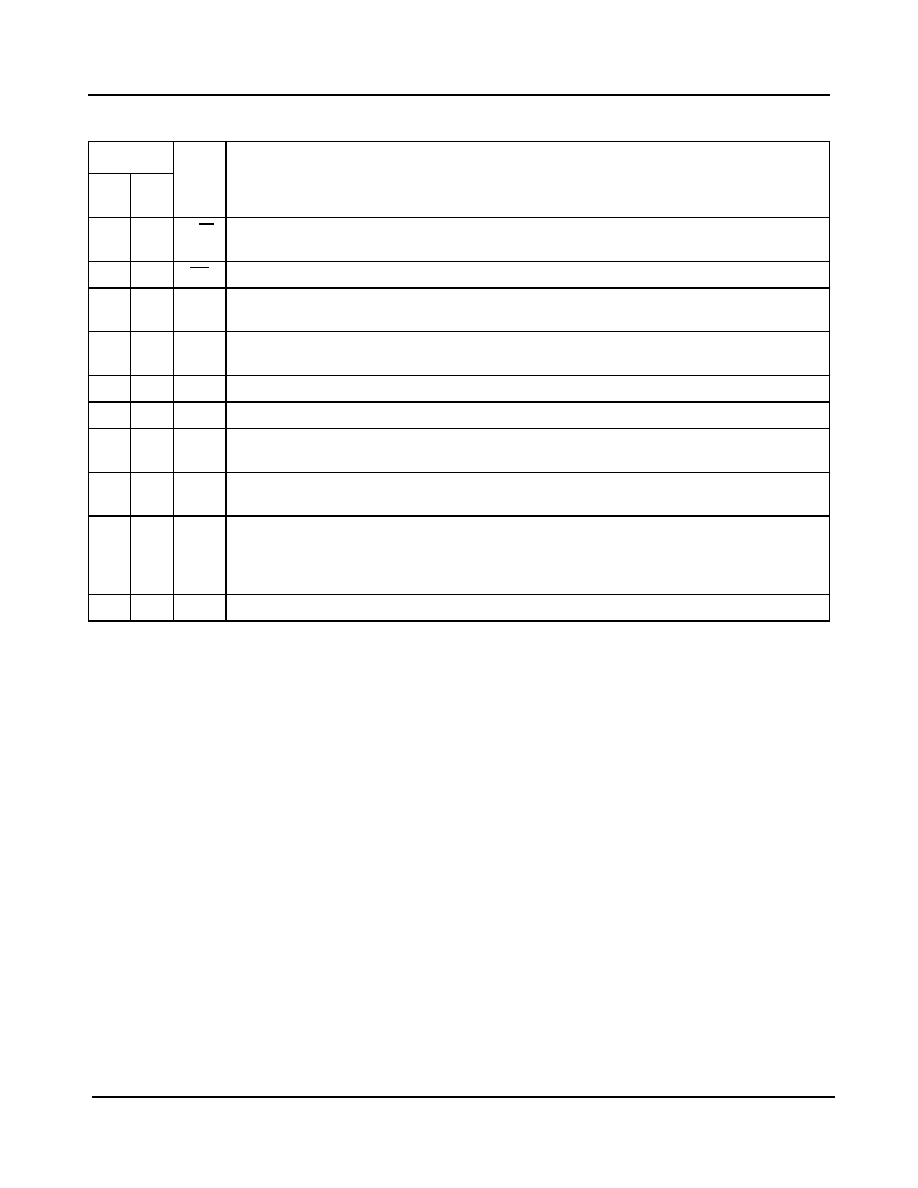
Pin Description
Pin #
Name
Description
40
DIP
44
PLCC
1
2
DTA Data Acknowledgement (Open Drain Output). This is the data acknowledgement on the
microprocessor interface. This pin is pulled low to signal that the chip has processed the data. A
909
, 1/4 W, resistor is recommended to be used as a pullup.
2-4
3-5
STi0-
STi2
ST-BUS Input 0 to 2 (Inputs). These are the inputs for the 2048 kbit/s ST-BUS input streams.
5
7
STi3 ST-BUS Input 3 (Input). These are the inputs for the 2048 kbit/s ST-BUS input streams.
6-9
8-11
IC
Internal Connections. Must be connected to V
DD
.
10
12
V
DD
Power Input. Positive Supply.
11
13
F0i
Framing 0-Type (Input). This is the input for the frame synchronization pulse for the 2048 kbit/s
ST-BUS streams. A low on this input causes the internal counter to reset on
the next negative
transition of C4i.
12
14
C4i
4.096 MHz Clock (Input). ST-BUS bit cell boundaries lie on the alternate falling edges of this clock.
13-15 15-17 A0-A2 Address 0 to 2 (Inputs). These are the inputs for the address lines on the microprocessor interface.
16-18 19-21 A3-A5 Address 3 to 5 (Inputs). These are the inputs for the address lines on the microprocessor interface
19
22
DS
Data Strobe (Input). This is the input for the active high data strobe on the microprocessor interface.
1
6
5
4
3
2
44
43
42
41
40
7
8
9
10
11
12
13
14
15
16
39
38
37
36
35
34
33
32
31
30
23
18
19
20
21
22
24
25
26
27
28
17
29
STi3
IC
IC
IC
IC
VDD
F0i
C4i
A0
A1
A2
STo3
IC
IC
IC
IC
VSS
D0
D1
D2
D3
D4
NC
STi
1
DTA
ODE
STo1
NC
NC
A4
DS
CS
D6
NC
A3
A5
R/W
D7
D5
44 PIN PLCC
DTA
STi0
STi1
STi2
STi3
IC
IC
IC
IC
VDD
F0i
C4i
A0
A1
A2
A3
A4
A5
DS
IC
ODE
STo0
STo1
STo2
STo3
IC
IC
IC
IC
VSS
D0
D1
D2
D3
D4
D5
D6
D7
CS
2
3
4
5
6
7
8
9
10
11
12
13
14
15
16
17
18
19
20
1
R/W
40
39
38
37
36
35
34
33
32
31
30
29
28
27
26
25
24
23
22
21
40 PIN PLASTIC DIP
STi
2
STi
0
IC
STo
0
STo
2
MT8981D
Data Sheet
3
Zarlink Semiconductor Inc.
Functional Description
In recent years, there has been a trend in telephony towards digital switching, particularly in association with
software control. Simultaneously, there has been a trend in system architectures towards distributed processing or
multi-processor systems.
In accordance with these trends, Zarlink has devised the ST-BUS (Serial Telecom Bus). This bus architecture can
be used both in software-controlled digital voice and data switching, and for interprocessor communications. The
uses in switching and in interprocessor communications are completely integrated to allow for a simple general
purpose architecture appropriate for the systems of the future.
The serial streams of the ST-BUS operate continuously at 2048 kbit/s and are arranged in 125
µs wide frames
which contain 32 8-bit channels. Zarlink manufactures a number of devices which interface to the ST-BUS; a key
device being the MT8981 chip.
The MT8981 can switch data from channels on ST-BUS inputs to channels on ST-BUS outputs, and simultaneously
allows its controlling microprocessor to read channels on ST-BUS inputs or write to channels on ST-BUS outputs
(Message Mode). To the microprocessor, the MT8981 looks like a memory peripheral. The microprocessor can
write to the MT8981 to establish switched connections between input ST-BUS channels and output ST-BUS
channels, or to transmit messages on output ST-BUS channels. By reading from the MT8981, the microprocessor
can receive messages from ST-BUS input channels or check which switched connections have already been
established.
By integrating both switching and interprocessor communications, the MT8981 allows systems to use distributed
processing and to switch voice or data in an ST-BUS architecture.
20
23
R/W Read or Write (Input). This is the input for the read/write signal on the microprocessor interface -
high for read, low for write.
21
24
CS
Chip Select (Input). This is the input for the active low chip select on the microprocessor interface.
22-24 25-27 D7-D5 Data 7 to 5 (Three-state I/O Pins). These are the bidirectional data pins on the microprocessor
interface.
25-29 29-33 D4-D0 Data 4 to 0 (Three-state I/O Pins). These are the bidirectional data pins on the microprocessor
interface.
30
34
V
SS
Power Input. Negative Supply (Ground).
31-34 35-38
IC
Internal Connections. Leave pins disconnected.
35
39
STo3 ST-BUS Output 3 (Three-state Outputs). These are the pins for the four 2048 kbit/s ST-BUS output
streams.
36-38 41-43 STo2-
STo0
ST-BUS Output 2 to 0 (Three-state Outputs). These are the pins for the four 2048 kbit/s ST-BUS
output streams.
39
44
ODE Output Drive Enable (Input). If this input is held high, the STo0-STo3 output drivers function
normally. If this input is low, the STo0-STo3 output drivers go into their high impedance state. NB:
Even when ODE is high, channels on the STo0-STo3 outputs can go high impedance under software
control.
40
1
IC
Internal Connection. Leave pin disconnected.
Pin Description (continued)
Pin #
Name
Description
40
DIP
44
PLCC

MT8981D
Data Sheet
4
Zarlink Semiconductor Inc.
Hardware Description
Serial data at 2048 kbit/s is received at the four ST-BUS inputs (STi0 to STi3), and serial data is transmitted at the
four ST-BUS outputs (STo0 to STo3). Each serial input accepts 32 channels of digital data, each channel containing
an 8-bit word which may represent a PCM-encoded analog/voice sample as provided by a codec (e.g., Zarlink's
MT8964).
This serial input word is converted into parallel data and stored in the 128 X 8 Data Memory. Locations in the Data
Memory are associated with particular channels on particular ST-BUS input streams. These locations can be read
by the microprocessor which controls the chip.
Locations in the Connection Memory, which is split into high and low parts, are associated with particular ST-BUS
output streams. When a channel is due to be transmitted on an ST-BUS output, the data for the channel can either
be switched from an ST-BUS input or it can originate from the microprocessor. If the data is switched from an input,
then the contents of the Connection Memory Low location associated with the output channel is used to address
the Data Memory. This Data Memory address corresponds to the channel on the input ST-BUS stream on which the
data for switching arrived. If the data for the output channel originates from the microprocessor (Message Mode),
then the contents of the Connection Memory Low location associated with the output channel are output directly,
and this data is output repetitively on the channel once every frame until the microprocessor intervenes.
The Connection Memory data is received, via the Control Interface, at D7 to D0. The Control Interface also receives
address information at A5 to A0 and handles the microprocessor control signals CS, DTA, R/W and DS. There are
two parts to any address in the Data Memory or Connection Memory. The higher order bits come from the
Control Register, which may be written to or read from via the Control Interface. The lower order bits come from the
address lines directly.
The Control Register also allows the chip to broadcast messages on all ST-BUS outputs (i.e., to put every channel
into Message Mode), or to split the memory so that reads are from the Data Memory and writes are to the
Connection Memory Low. The Connection Memory High determines whether individual output channels are in
Message Mode, and allows individual output channels to go into a high-impedance state, which enables arrays of
MT8981s to be constructed. It also controls the CSTo pin.
All ST-BUS timing is derived from the two signals C4i and F0i.

MT8981D
Data Sheet
5
Zarlink Semiconductor Inc.
Figure 3 - Address Memory Map
Software Control
The address lines on the Control Interface give access to the Control Register directly or, depending on the
contents of the Control Register, to the High or Low sections of the Connection Memory or to the Data Memory.
If address line A5 is low, then the Control Register is addressed regardless of the other address lines (see Fig. 3). If
A5 is high, then the address lines A4-A0 select the memory location corresponding to channel 0-31 for the memory
and stream selected in the Control Register.
The data in the Control Register consists of mode control bits, memory select bits, and stream address bits (see
Fig. 4). The memory select bits allow the Connection Memory High or Low or the Data Memory to be chosen, and
the stream address bits define one of the ST-BUS input or output streams.
Bit 7 of the Control Register allows split memory operation - reads are from the Data Memory and writes are to the
Connection Memory Low.
The other mode control bit, bit 6, puts every output channel on every output stream into active Message Mode; i.e.,
the contents of the Connection Memory Low are output on the ST-BUS output streams once every frame unless the
ODE pin is low. In this mode the chip behaves as if bits 2 and 0 of every Connection Memory High location were 1,
regardless of the actual values.
A5
A4
A3
A2
A1
A0
HEX ADDRESS
LOCATION
0
1
1
Ј
Ј
Ј
1
X
0
0
Ј
Ј
Ј
1
X
0
0
Ј
Ј
Ј
1
X
0
0
Ј
Ј
Ј
1
X
0
0
Ј
Ј
Ј
1
X
0
1
Ј
Ј
Ј
1
00 - 1F
20
21
Ј
Ј
Ј
3F
Control Register *
Channel 0
Channel 1
Ј
Ј
Ј
Channel 31
* Writing to the Control Register is the only fast transaction.
Memory and stream are specified by the contents of the Control Register.