1
Features
∑
3.3 volt supply
∑
5V tolerant inputs and TTL compatible outputs.
∑
256 x 256 or 512 x 256 switching configurations
∑
8-bit or 4-bit channel switching capability
∑
Guarantees frame integrity for wideband
channels
∑
Automatic identification of ST-BUS/GCI
interfaces
∑
Accepts serial streams with data rates of 2.048,
4.096 or 8.192 Mb/s
∑
Rate conversion from 2.048 Mb/s to 4.096 or
8.192 Mb/s and vice-versa
∑
Programmable frame offset on inputs
∑
Per-channel three-state control
∑
Per-channel message mode
∑
Control interface compatible to Intel/Motorola
CPUs
∑
Low power consumption
Applications
∑
Medium size mixed voice and data switching/
processing matrices
∑
Hyperchannel switching (e.g., ISDN H0)
∑
MVIP
TM
interface functions
∑
Serial bus control and monitoring
∑
Centralized voice processing systems
∑
Voice/Data multiplexer
∑
ADPCM 32 kbit/s channel switching
Description
The 3.3V Multiple Rate Digital Switch (MT89L86) is
pin compatible with Zarlink's 5V MT8986 and retains
all of its functionality. This 3.3v device is designed to
provide simultaneous non-blocking connections for
up to 256 64kb/s channels or blocking connections
for up to 512 64kb/s channels. The serial inputs and
outputs may have 32 to 128 64kb/s channels per
frame with data rates ranging from 2048 up to 8192
kb/s. It also provides per-channel selection between
variable and constant throughput delays allowing
voice and grouped data channels to be switched
without corrupting the data sequence integrity.
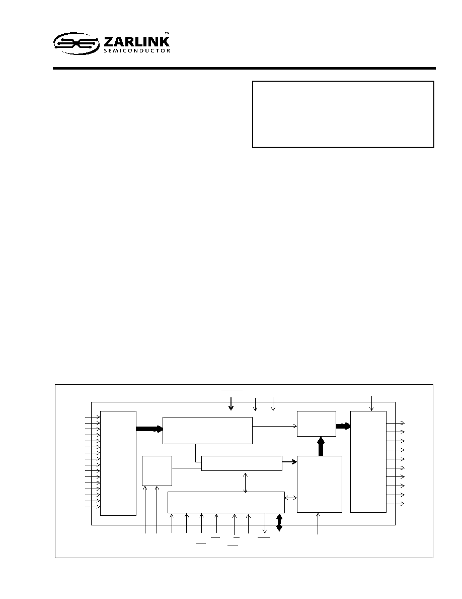
Figure 1 - Functional Block Diagram
STi0
STi1
STi2
STi3
STi4
STi5
STi6
STi7
STi8
STi9
STi10
STi11
STi12
STi13
STi14
STi15
STo0
STo1
STo2
STo3
STo4
STo5
STo6
STo7
STo8
STo9
CLK FR AS/
ALE
IM
DS
RD
CS
R/W
WR
A0/
A7
DTA AD7/
AD0
CSTo
V
DD
V
SS
ODE
Serial
to
Parallel
Converter
Multiple Buffer Data
Memory
Output
MUX
Parallel
to
Serial
Converter
Timing
Unit
Internal Registers
Microprocessor
Interface
Connection
Memory
RESET
** for 48-pin SSOP only
**
DS5195
ISSUE 2
September 1999
MT89L86
Multiple Rate Digital Switch
CMOS ST-BUS
FAMILY
Ordering Information
MT89L86AP
44 Pin PLCC
MT89L86AN
48 Pin SSOP
-40
∞
C to +85
∞
C
Advance Information

MT89L86
Advance Information
2
Figure 2 - Pin Connections
Pin Description
Pin #
Name
Description
44
PLCC
48
SSOP
2
2
DTA
Data Acknowledgment
(Open Drain Output)
.
This active low output indicates that a
data bus transfer is complete. A pull-up resistor is required at this output.
3-5
7-9
3-5
7-9
STi0-5
ST-BUS Inputs 0 to 5
(5V-tolerant Inputs). Serial data input streams. These streams
may have data rates of 2.048, 4.096 or 8.192 Mbit/s with 32, 64 or 128 channels,
respectively.
10
10
STi6/A6
ST-BUS Input 6/Addr.6 input
(5V-tolerant Input). The function of this pin is determined
by the switching configuration enabled. If non-multiplexed CPU bus is used along with a
higher input rate of 8.192 or 4.096 Mb/s, this pin provides A6 address input function.
For 2.048 and 4.096 Mb/s (8x4) applications or when the multiplexed CPU bus
interface is selected, this pin assumes STi6 function. See Control Register bits
description and Tables 1, 2, 6 & 7 for more details.
Note that for applications where both A6 and STi6 inputs are required simultaneously
(e.g., 8 x 4 switching configuration at 4.096 Mb/s or rate conversion between 2.048Mb/
s to 4.196 or 8.192 Mb/s) the A6 input should be connected to pin STo6/A6.
11
11
STi7/A7
ST-BUS Input 7/Addr.7 input
(5V-tolerant Input): The function of this pin is determined
by the switching configuration enabled. If non-multiplexed CPU bus is used along with a
higher input rate of 8.192 Mb/s, this pin provides A7 address input function.
For 2.048 and 4.096 Mb/s (8x4) applications or when the multiplexed CPU bus is
selected, this pin assumes STi7 function. See Control Register bits description and
Tables 1, 2, 6 & 7 for more details.
Note that for applications where both A7 and STi7 inputs are required simultaneously
(e.g., 2.048 to 8.192 Mb/s rate conversion) the A7 input should be connected to pin
STo7/A7.
2
3
4
5
6
7
8
9
10
11
12
13
14
15
16
17
18
19
20
1
48 PIN SSOP
47
46
45
44
43
42
41
40
39
38
37
36
35
34
33
32
31
30
29
28
ODE
STo0
STo1
STo2
STi14/STo8
STo3
STo4
STo5
STo6/A6
STo7/A7
V
SS
V
DD
AD0
AD1
AD2
AD3
AD4
STi15/STo9
AD5
AD6
DTA
STi0
STi1
STi2
AS/ALE
STi3
STi4
STi5
STi6/A6
STi7/A7
V
DD
RESET
FR
CLK
STi8/A0
STi9/A1
STi10/A2
IM
STi11/A3
STi12/A4
1
6 5 4 3 2
44 43 42 41 40
7
8
9
10
11
12
13
14
15
16
39
38
37
36
35
34
33
32
31
30
23
18 19 20 21 22
24 25 26 27 28
17
29
D
T
A
STi0
STi1
STi2
AS/ALE
ODE
STo0
STo1
STo2
STi14/STo8
STo3
STo4
STo5
STo6/A6
STo7/A7
V
SS
AD0
AD1
AD2
AD3
AD4
IM
STi11/A3
STi12/A4
STi13/A5
DS/R
D
STi15/STo9
AD5
AD6
AD7
C
S
R/W
/
W
R
CSTo
STi3
STi4
STi5
STi6/A6
STi7/A7
V
DD
FR
CLK
STi8/A0
STi9/A1
STi10/A2
44 PIN PLCC
48
CSTo
V
SS
21
27
AD7
STi13/A5
22
26
CS
DS/RD
23
25
V
SS
R/W\WR
24
(JEDEC MO-118, 300mil Wide)
Advance Information
MT89L86
3
12
12,36
V
DD
+3.3 Volt Power Supply
.
13
RESET
Device Reset
( 5v-tolerant input). This pin is only available for the 48-pin SSOP
package. In normal operation, This active low input puts the MT89L86 in its reset state.
It clears the internal counters and registers. All ST-BUS outputs are set to the high
impedance state. The RESET pin must be held low for a minimum of 100nsec to reset
the device.
13
14
FR
Frame Pulse
(5V-tolerant Input). This input accepts and automatically identifies frame
synchronization signals formatted according to ST-BUS and GCI interface
specifications.
14
15
CLK
Clock
(5V-tolerant Input). Serial clock for shifting data in/out on the serial streams.
Depending on the serial interface speed selected by IMS (Interface Mode Select)
register, the clock at this pin can be 4.096 or 8.192 MHz.
15-17 16-18
STi8/A0,
STi9/A1,
STi10/A2
Address 0-2 / Input Streams 8-10
(5V-tolerant Input). When the non-multiplexed CPU
bus is selected, these lines provide the A0-A2 address lines to the MT89L86 internal
registers. When the 16x8 switching configuration is selected, these pins are ST-BUS
serial inputs 8 to 10 receiving data at 2.048 Mb/s.
19-21 20-22 STi11/A3,
STi12/A4,
STi13/A5
Address 3-5 / Input Streams 11-13
(5V-tolerant Input). When the non-multiplexed
CPU bus is selected, these lines provide the A3-A5 address lines to the MT89L86
internal registers. When the 16x8 switching configuration is selected, these pins are
ST-BUS serial inputs 11 to 13 receiving data at 2.048 Mb/s.
22
23
DS/RD
Data Strobe/Read
(5V-tolerant Input). When the non-multiplexed CPU bus or Motorola
multiplexed bus is selected, this input is DS. This active high input works in conjunction
with CS to enable read and write operation.
For the Intel/National multiplexed bus interface, this input is RD. This active low input
configures the data bus lines (AD0-7) as outputs.
23
24
R/W\WR
Read/Write \ Write
(5V-tolerant Input). For the non-multiplexed or Motorola multiplexed
bus interface, this input is R/W. This input controls the direction of the data bus lines
(AD0-AD7) during a microprocessor access.
For the Intel/National multiplexed bus interface, this input is WR. This active low signal
configures the data bus lines (AD0-7) as inputs.
24
26
CS
Chip Select
(5V-tolerant Input). This active low input enables a microprocessor read
or write of the MT89L86's internal control register or memories.
25-27
29-33
27-29
31-35
AD7-AD0
Data Bus
(Bidirectional): These pins provide microprocessor access to the internal
control registers, connection memories high and low and data memories. For the
multiplexed bus interface these pins also provide the input address to the internal
Address Latch circuit.
34
1,
25,37
V
SS
Ground.
35
38
STo7/A7
ST-BUS Output 7/Address 7 input (Three-state output/input). The function of this pin
is determined by the switching configuration enabled. If non-multiplexed CPU bus is
used along with data rates employing 8.192 Mb/s rates, this pin provides A7 address
input function. For 2.048 Mb/s applications or when the multiplexed CPU bus interface
is selected, this pin assumes STo7 function. See Tables 1, 2, 6 & 7 for more details.
Note that for applications where A7 input and STo7 output are required simultaneously
(e.g., 8.192 to 2.048 Mb/s rate conversion), the A7 input should be connected to pin
STi7/A7.
Pin Description (continued)
Pin #
Name
Description
44
PLCC
48
SSOP

MT89L86
Advance Information
4
36
39
STo6/A6
ST-BUS Output 6/Address 6 input (Three-state output/input). The function of this
pin is determined by the switching configuration enabled. If non-multiplexed CPU bus is
used along with a higher data rate employing 8.192 or 4.096 Mb/s, this pin provides the
A6 address input function. For 2.048 Mb/s applications or when the multiplexed CPU
bus interface is selected, this pin assumes STo6 function. See Tables 1, 2, 6 & 7 for
more details.
Note that for applications where both A6 input and STo6 output are required
simultaneously (e.g., 4.096 to 2.048 Mb/s or 8.192 to 2.048 Mb/s rate conversion
applications), the A6 input should be connected to pin STi6/A6.
37-39
41-43
40-42
44-46
STo5-0
ST-BUS Outputs 5 to 0 (Three-state Outputs). Serial data output streams. These
serial streams may be composed of 32, 64 and 128 channels at data rates of 2.048,
4.096 or 8.192 Mbit/s, respectively.
44
47
ODE
Output Drive Enable (5V-tolerant Input). This is the output enable input for the STo0
to STo9 serial outputs. If this input is low STo0-9 are high impedance. If this input is
high each channel may still be set to high impedance by using per-channel control bits
in Connect Memory High.
1
48
CSTo
Control ST-BUS Output (Output). This is a 2.048 Mb/s output containing 256 bits per
frame. The level of each bit is determined by the CSTo bit in the Connect Memory high
locations.
6
6
AS/ALE
Address Strobe or Latch Enable (5V-tolerant Input). This input is only used if
multiplexed bus is selected via the IM input pin.
The falling edge of this signal is used to sample the address into the address latch
circuit. When the non-multiplexed bus interface is selected, this input is not required
and should be connected to ground.
18
19
IM
CPU Interface Mode (5V-tolerant Input). If HIGH, this input configures the MT89L86
in the multiplexed microprocessor bus mode. When this input pin is connected to
ground, the MT89L86 assumes non-multiplexed CPU interface.
28
30
STi15/
STo9
ST-BUS Input 15 / ST-BUS Output 9 (Input/three-state output). This pin is only used
if multiplexed CPU bus is selected. If 16-input x 8-output switching configuration is
enabled in the SCB bits (IMS register), this pin is an input receiving serial ST-BUS
stream 15 at a data rate of 2.048 Mbit/s.
If Stream Pair Selection capability is enabled (see switching configuration section), this
pin is the ST-BUS stream 9 output.
When non-multiplexed bus structure is used, this pin should be connected to ground.
40
43
STi14/
STo8
ST-BUS Input 14 / ST-BUS Output 8 (Input/three-state output). This pin is only used
if multiplexed CPU bus is selected. If 16-input x 8-output switching configuration is
enabled in the SCB bits (IMS register), this pin is an input that receives serial ST-BUS
stream 14 at a data rate of 2.048 Mbit/s.
If Stream Pair Selection capability is enabled (see switching configuration section), this
pin is the ST-BUS stream 8 output.
When non-multiplexed bus structure is used, this pin should be connected to ground.
Pin Description (continued)
Pin #
Name
Description
44
PLCC
48
SSOP

Advance Information
MT89L86
5
Device Overview
With the integration of voice, video and data services
in the same network, there has been an increasing
demand for systems which ensure that data at N x 64
kb/s rates maintain sequence integrity while being
transported through time-slot interchange circuits.
This requirement demands time-slot interchange
devices which perform switching with constant
throughput delay for wideband data applications
while maintaining minimum delay for voice channels.
The MT89L86 device meets the above requirement
and allows existing systems based on the MT8980D
to be easily upgraded to maintain the data integrity
when wideband data is transported. The device is
designed to switch 32, 64 or N x 64 bit/s data. This
MT89L86 can provide frame integrity for data
applications and minimum throughput switching
delay for voice applications on a per channel basis.
The serial streams of the MT89L86 can operate at
2.048, 4.096 or 8.192 Mbit/s and are arranged in 125
µs wide frames which contain 32, 64 and 128
channels, respectively. In addition, a built-in rate
conversion circuit allows the user to interconnect
various backbone speeds like 2.048 or 4.096 or
8.192 Mb/s while maintaining the control of
throughput delay function on a per-channel basis.
By using Zarlink Message mode capability, the
microprocessor can access input and output time-
slots on a per channel basis to control external
circuits or other ST-BUS devices. This MT89L86
automatically identifies the polarity of the frame
synchronization input signal and configures its serial
port to be compatible to both ST-BUS and GCI
formats.
Two different microprocessor bus interfaces can be
selected through an input mode pin (IM): Non-
Multiplexed or Multiplexed. These interfaces provide
compatibility with Intel/National multiplexed and
Motorola Multiplexed/Non-Multiplexed buses. The
MT89L86 provides a 16 x 8 switching configuration
to form a 512 x 256 channel blocking matrix. Also, a
flexible Stream Pair Selection operation allows the
software selection of which pair of input and output
streams can be connected to an internal 128 x 128
matrix. See Switching Configurations section for
details.
Functional Description
A functional Block Diagram of the 3.3V MT89L86 is
shown in Figure 1. Depending on the application,
TDM serial data can be received at different rates
and from different number of serial streams.
Data and Connect Memories
For all data rates, the received serial data is
converted to parallel format by the serial to parallel
converters and stored sequentially in a Data
Memory. Depending on the selected operation
programmed in the IMS (Interface Mode Select)
register, the Data Memory may have up to 512 bytes
in use. The sequential addressing of the Data
Memory is performed by an internal counter which is
reset by the input 8 kHz frame pulse (FR) marking
the frame boundaries of the incoming serial data
streams.
Data to be output on the serial streams may come
from two sources: Data Memory or Connect Memory.
Locations in the Connect Memory, which is split into
HIGH and LOW parts, are associated with particular
ST-BUS output streams. When a channel is due to be
transmitted on an ST-BUS output, the data for the
channel can either be switched from an ST-BUS
input as in connection mode or it can be from the
Connect Memory Low as in message mode. Data
destined for a particular channel on the serial output
stream is read from the Data Memory or Connect
Memory Low during the previous channel time-slot.
This allows enough time for memory access and
parallel to serial conversion.
Connection and Message Modes
In the connection mode, the addresses of the input
source data for all output channels are stored in the
Connect memories High (CMH) and Low (CML). The
CML and CMH are mapped so that each location
corresponds to an output channel on the output
streams. The number of source address bits in CMH
and CML to be utilized varies according to the
switching configuration selected in the IMS register.
For details on the use of the source address data
(CAB and SAB bits), see CMH and CML bit describe-
thin (Figures 5 & 6). Once the source address bits
are programmed by the CPU, the contents of the
Data Memory at the selected address are transferred
to the parallel-to-serial converters. By having the
output channel specify the source channel through
the connect memory, the user can route the same
input channel to several output channels, allowing
broadcast facility within the switch.
In the message mode the CPU writes data to the
Connect Memory Low locations corresponding to the
output link and channel number. The contents of the
Connect Memory Low are transferred directly to the
parallel-to-serial converter one channel before it is to