 | –≠–ª–µ–∫—Ç—Ä–æ–Ω–Ω—ã–π –∫–æ–º–ø–æ–Ω–µ–Ω—Ç: MT9043AN | –°–∫–∞—á–∞—Ç—å:  PDF PDF  ZIP ZIP |

1
Zarlink Semiconductor Inc.
Zarlink, ZL and the Zarlink Semiconductor logo are trademarks of Zarlink Semiconductor Inc.
Copyright 2003, Zarlink Semiconductor Inc. All Rights Reserved.
Features
∑ Supports AT&T TR62411 and Bellcore GR-1244-
CORE, Stratum 4 Enhanced and Stratum 4 timing
for DS1 interfaces
∑ Supports ETSI ETS 300 011, TBR 4, TBR 12 and
TBR 13 timing for E1 interfaces
∑ Selectable 19.44 MHz, 1.544MHz, 2.048MHz or
8kHz input reference signals
∑ Provides C1.5, C2, C4, C6, C8, C16, and C19
(STS-3/OC3 clock divided by 8) output clock
signals
∑ Provides 5 different styles of 8 KHz framing
pulses
∑ Attenuates wander from 1.9Hz
∑ Fast lock mode
∑ Provides Time Interval Error (TIE) correction
∑ Accepts reference inputs from two independent
sources
∑ JTAG Boundary Scan
Applications
∑ Synchronization and timing control for multitrunk
T1,E1 and STS-3/OC3 systems
∑ ST-BUS clock and frame pulse sources
Description
The MT9043 T1/E1 System Synchronizer contains a
digital phase-locked loop (DPLL), which provides timing
and synchronization signals for multitrunk T1 and E1
primary rate transmission links.
The MT9043 generates ST-BUS clock and framing
signals that are phase locked to either a 19.44 MHz,
2.048MHz, 1.544MHz, or 8kHz input reference.
The MT9043 is compliant with AT&T TR62411 and
Bellcore GR-1244-CORE, Stratum 4 Enhanced, and
Stratum 4; and ETSI ETS 300 011. It will meet the
jitter/wander tolerance, jitter transfer, intrinsic jitter,
frequency accuracy, capture range, phase change
slope, and MTIE requirements for these specifications.
November 2003
Ordering Information
MT9043AN 48 pin SSOP
-40
∞
C to +85
∞
C
MT9043
T1/E1 System Synchronizer
Data Sheet
Figure 1 - Functional Block Diagram
Zarlink Semiconductor US Patent No. 5,602,884, UK Patent No. 0772912,
France Brevete S.G.D.G. 0772912; Germany DBP No. 69502724.7-08
IEEE
1149.1a
Reference
Select
Feedback
TIE
Corrector
Enable
Control State Machine
DPLL
State
Select
State
Select
Frequency
Select
MUX
Input
Impairment
Monitor
Output
Interface
Circuit
Reference
Select
MUX
TIE
Corrector
Circuit
MS
FS1
FS2
TCK
SEC
RST
RSEL
VDD
VSS
TCLR
C1.5o
C19o
C2o
C4o
C8o
C16o
F0o
F8o
F16o
OSCo
OSCi
Master Clock
TDO
PRI
TDI
TMS
TRST
C6o
RSP
TSP
FLOCK
LOCK
Virtual
Reference
Selected
Reference
IM
MT9043
Data Sheet
2
Zarlink Semiconductor Inc.
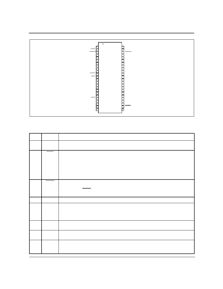
Figure 2 - Pin Connections
Pin Description
Pin #
Name
Description
1,10,
23,31
V
SS
Ground. 0 Volts. (Vss pads).
2
RST
Reset (Input). A logic low at this input resets the MT9043. To ensure proper operation, the
device must be reset after reference signal frequency changes and power-up. The RST
pin should be held low for a minimum of 300ns. While the RST pin is low, all frame pulses
except RST and TSP and all clock outputs except C6o, C16o and C19o are at logic high.
The RST, TSP, C6o and C16o are at logic low during reset. The C19o is free-running
during reset. Following a reset, the input reference source and output clocks and frame
pulses are phase aligned as shown in Figure 12.
3
TCLR
TIE Circuit Reset (Input). A logic low at this input resets the Time Interval Error (TIE)
correction circuit resulting in a realignment of input phase with output phase as shown in
Figure 13. The TCLR pin should be held low for a minimum of 300ns. This pin is internally
pulled down to VSS.
4
IC
Internal Connection. Leave open circuit.
5
SEC
Secondary Reference (Input). This is one of two (PRI & SEC) input reference sources
(falling edge) used for synchronization. One of four possible frequencies (8kHz, 1.544MHz,
2.048MHz or 19.44MHz) may be used. The selection of the input reference is based upon the
MS, and RSEL, control inputs.This pin is internally pulled up to V
DD
.
6
PRI
Primary Reference (Input). See pin description for SEC. This pin is internally pulled up to
V
DD
.
7,17
28,35
V
DD
Positive Supply Voltage. +3.3V
DC
nominal.
8
OSCo
Oscillator Master Clock (CMOS Output). For crystal operation, a 20MHz crystal is
connected from this pin to OSCi, see Figure 9. Not suitable for driving other devices. For
clock oscillator operation, this pin is left unconnected, see Figure 8.
2
3
4
5
6
7
8
9
10
11
12
13
14
15
16
17
18
19
20
1
47
46
45
44
43
42
41
40
39
38
37
36
35
34
33
32
31
30
29
28
TRST
TDI
TDO
IC
IC
FS1
FS2
IC
RSEL
IC
MS
Vdd
IC
IC
NC
Vss
IC
IM
Vdd
RST
IC
SEC
PRI
Vdd
OSCo
OSCi
Vss
F16o
TSP
F8o
C1.5o
C2o
C4o
C19o
48
TMS
V
SS
21
27
C6o
FLOCK
22
26
Vss
23
25
C8o
IC
24
C16o
MT9043AN
TCK
RSP
F0o
TCLR
Vdd
LOCK
MT9043
Data Sheet
3
Zarlink Semiconductor Inc.
9
OSCi
Oscillator Master Clock (CMOS Input). For crystal operation, a 20MHz crystal is
connected from this pin to OSCo, see Figure 9. For clock oscillator operation, this pin is
connected to a clock source, see Figure 8.
11
F16o
Frame Pulse ST-BUS 8.192 Mb/s (CMOS Output). This is an 8kHz 61ns active low framing
pulse, which marks the beginning of an ST-BUS frame. This is typically used for ST-BUS
operation at 8.192 Mb/s. See Figure 14.
12
F0o
Frame Pulse ST-BUS 2.048Mb/s (CMOS Output). This is an 8kHz 244ns active low framing
pulse, which marks the beginning of an ST-BUS frame. This is typically used for ST-BUS
operation at 2.048Mb/s and 4.096Mb/s. See Figure 14.
13
RSP
Receive Sync Pulse (CMOS Output). This is an 8kHz 488ns active high framing pulse,
which marks the beginning of an ST-BUS frame. This is typically used for connection to the
Siemens MUNICH-32 device. See Figure 15.
14
TSP
Transmit Sync Pulse (CMOS Output). This is an 8kHz 488ns active high framing pulse,
which marks the beginning of an ST-BUS frame. This is typically used for connection to the
Siemens MUNICH-32 device. See Figure 15.
15
F8o
Frame Pulse (CMOS Output). This is an 8kHz 122ns active high framing pulse, which marks
the beginning of a frame. See Figure 14.
16
C1.5o
Clock 1.544MHz (CMOS Output). This output is used in T1 applications.
18
LOCK
Lock Indicator (CMOS Output). This output goes high when the PLL is frequency locked to
the input reference.
19
C2o
Clock 2.048MHz (CMOS Output). This output is used for ST-BUS operation at 2.048Mb/s.
20
C4o
Clock 4.096MHz (CMOS Output). This output is used for ST-BUS operation at 2.048Mb/s
and 4.096Mb/s.
21
C19o
Clock 19.44MHz (CMOS Output). This output is used in OC3/STS3 applications.
22
FLOCK
Fast Lock Mode (Input). Set high to allow the PLL to quickly lock to the input reference (less
than 500 ms locking time).
24
IC
Internal Connection. Tie low for normal operation.
25
C8o
Clock 8.192MHz (CMOS Output). This output is used for ST-BUS operation at 8.192Mb/s.
26
C16o
Clock 16.384MHz (CMOS Output). This output is used for ST-BUS operation with a
16.384MHz clock.
27
C6o
Clock 6.312 Mhz (CMOS Output). This output is used for DS2 applications.
29
IM
Impairment Monitor (CMOS Output). A logic high on this pin indicates that the Input
Impairment Monitor has automatically put the device into Freerun Mode.
30
IC
Internal Connection. Tie high for normal operation.
32
NC
No Connection. Leave open circuit.
33,34
IC
Internal Connection. Tie low for normal operation.
36
MS
Mode/Control Select (Input). This input determines the state (Normal or Freerun) of
operation. The logic level at this input is gated in by the rising edge of F8o. See Table 3.
37
IC
Internal Connection. Tie low for normal operation.
Pin Description
Pin #
Name
Description

MT9043
Data Sheet
4
Zarlink Semiconductor Inc.
Functional Description
The MT9043 is a Multitrunk System Synchronizer, providing timing (clock) and synchronization (frame) signals to
interface circuits for T1 and E1 Primary Rate Digital Transmission links. Figure 1 is a functional block diagram which
is described in the following sections.
Reference Select MUX Circuit
The MT9043 accepts two simultaneous reference input signals and operates on their falling edges. Either the
primary reference (PRI) signal or the secondary reference (SEC) signal can be selected as input to the TIE
Corrector Circuit. The selection is based on the Control, Mode and Reference Selection of the device. See Table 1
and Table 4.
Frequency Select MUX Circuit
The MT9043 operates with one of four possible input reference frequencies (8kHz, 1.544MHz, 2.048MHz or
19.44MHz). The frequency select inputs (FS1 and FS2) determine which of the four frequencies may be used at
the reference inputs (PRI and SEC). Both inputs must have the same frequency applied to them. A reset (RST)
must be performed after every frequency select input change. See Table 1.
38
RSEL
Reference Source Select (Input). A logic low selects the PRI (primary) reference source as
the input reference signal and a logic high selects the SEC (secondary) input. The logic level
at this input is gated in by the rising edge of F8o. See Table 2. This pin is internally pulled
down to VSS.
39
IC
Internal Connection. Tie low for normal operation.
40
FS2
Frequency Select 2 (Input). This input, in conjunction with FS1, selects which of four
possible frequencies (8kHz, 1.544MHz, 2.048MHz or 19.44MHz) may be input to the PRI and
SEC inputs. See Table 1.
41
FS1
Frequency Select 1 (Input). See pin description for FS2.
42
IC
Internal Connection. Tie Low for Normal Operation.
43
IC
Internal Connection. Leave Open Circuit.
44
TDO
Test Serial Data Out (CMOS Output). JTAG serial data is output on this pin on the falling
edge of TCK. This pin is held in high impedance state when JTAG scan is not enabled.
45
TDI
Test Serial Data In (Input). JTAG serial test instructions and data are shifted in on this pin.
This pin is internally pulled up to V
DD
.
46
TRST
Test Reset (Input). Asynchronously initializes the JTAG TAP controller by putting it in the
Test-Logic-Reset state. If not used, this pin should be held low.
47
TCK
Test Clock (Input). Provides the clock to the JTAG test logic. This pin is internally pulled up
to V
DD
.
48
TMS
Test Mode Select (Input). JTAG signal that controls the state transitions of the TAP
controller. This pin is internally pulled up to V
DD
.
Pin Description
Pin #
Name
Description

MT9043
Data Sheet
5
Zarlink Semiconductor Inc.
Time Interval Error (TIE) Corrector Circuit
The TIE corrector circuit, when enabled, prevents a step change in phase on the input reference signals (PRI or
SEC) from causing a step change in phase at the input of the DPLL block of Figure 1.
During reference input rearrangement, such as during a switch from the primary reference (PRI) to the secondary
reference (SEC), a step change in phase on the input signals will occur. A phase step at the input of the DPLL
would lead to unacceptable phase changes in the output signal.
As shown in Figure 3, the TIE Corrector Circuit receives one of the two reference (PRI or SEC) signals, passes the
signal through a programmable delay line, and uses this delayed signal as an internal virtual reference, which is
input to the DPLL. Therefore, the virtual reference is a delayed version of the selected reference.
Figure 3 - TIE Corrector Circuit
During a switch from one reference to the other, the State Machine first changes the mode of the device
from Normal to Freerun. The Compare Circuit then measures the phase delay between the current phase
(feedback signal) and the phase of the new reference signal. This delay value is passed to the Programmable
Delay Circuit (See Figure 3). The state machine then returns the device to Normal Mode and the DPLL begins
using the new virtual reference signal. The difference between the phase position of the new virtual reference and
the previous reference is less than 1
µ
s.
Since internal delay circuitry maintains the alignment between the old virtual reference and the new virtual
reference, a phase error may exist between the selected input reference signal and the output signal of the DPLL.
This phase error is a function of the difference in phase between the two input reference signals during reference
FS2
FS1
Input Frequency
0
0
19.44MHz
0
1
8kHz
1
0
1.544MHz
1
1
2.048MHz
Table 1 - Input Frequency Selection
Programmable
Delay Circuit
Control Signal
Delay Value
TCLR
Resets Delay
Compare
Circuit
TIE Corrector
Enable
from
State Machine
Control
Circuit
Feedback
Signal from
Frequency
Select MUX
PRI or SEC
from
Reference
Select Mux
Virtual
Reference
to DPLL