Document Outline
- Features
- Applications
- Description
- MT9072 Detailed Feature Summary
- 1.0 Change Summary
- 2.0 Overview
- 3.0 PCM24 Interface (T1)
- 4.0 PCM30 Interface (E1)
- 5.0 Framing
- 6.0 Elastic Buffer
- 7.0 Data Link
- 8.0 Signaling
- 9.0 HDLC
- 10.0 MT9072 Access and Control
- 10.1 Processor Interface (A11-A0, D15-D0, I/M, DS, R/W, CS, IRQ, Pins)
- 10.1.1 Framer and Register Access
- 10.1.2 ST-BUS Interface (DSTi, DSTo, CSTi, CSTo Pins)
- 10.1.3 IMA Interface (DSTi, DSTo, Pins)
- 10.1.4 Signaling Multiframe Boundary (RxMF, TxMF Pins)
- 10.1.5 Control Pins
- 10.1.6 Data Link (DL) Interface (RxDL, RxDLC, TxDL, TxDLC Pins)
- 10.1.7 Multiframe Boundary (RxMF, TxMF Pins)
- 11.0 ST-BUS Analyzer
- 12.0 Loopbacks
- 13.0 Performance Monitoring
- 14.0 Maintenance and Alarms
- 15.0 Interrupts
- 16.0 JTAG (Joint Test Action Group) Operation
- 17.0 MT9072 Register Set
- 18.0 Applications
- 19.0 AC/DC Electrical Characteristics
- 20.0 Applicable Specifications

1
Zarlink Semiconductor Inc.
Zarlink, ZL and the Zarlink Semiconductor logo are trademarks of Zarlink Semiconductor Inc.
Copyright 2004, Zarlink Semiconductor Inc. All Rights Reserved.
Features
�
Eight fully independent, T1/E1/J1 framers
�
3.3 V supply with 5 V tolerant inputs
�
Selectable 2.048 Mbit/s or 8.192 Mbit/s serial
buses for both data and signaling
�
Framing Modes:
- T1: D4, ESF, T1DM
- E1: Basic Framing, CRC4 multiframing and
Signaling Multiframing
�
Supports Inverse Mux for ATM
�
Timeslot assignable HDLC
�
IEEE-1149.1 (JTAG) test port
Applications
�
T1/E1/J1 add/drop multiplexers
�
V5.1 and V5.2 access network interfaces
�
CO and PBX equipment interfaces
�
Primary rate IDSN nodes
�
Digital Cross-connect Systems (DCS)
�
Wireless base stations
Description
The MT9072 is a multi-port T1/E1/J1 framing device
that integrates eight fully independent, feature rich
framers. The device is software selectable between T1,
E1 or J1 modes and meets the latest relevant
recommendations and standards from Telcordia, ANSI,
ETSI and ITU-T. An extensive suite of features make
the MT9072 very flexible and suitable for a wide variety
of applications around the globe.
October 2004
Ordering Information
MT9072AB
208 Pin LQFP
MT9072AV
220 Pin LBGA
-40
�C to +85�C
MT9072
Octal T1/E1/J1 Framer
Data Sheet
Figure 1 - Block Diagram
Microprocessor Interface
RW CS
DS
IRQ
D15~D0 A11~A0
IM
ST-BUS
Interface
CAS
Buffer
ST-BUS
Payload
National
Alarm Detection, 2 Frame Slip Buffer
ST-BUS
Interface
TPOS[0]
RPOS[0]
CSTi [0]
DSTi [0]
CSTo[0]
DSTo[0]
EXCLi[0]
RNEG[0]
TNEG[0]
Bit Buffer
CKi[0]
RxMF[0]
TxCL [0]
Transmit Framing, Error and
Test Signal Generation
Data Link
Receive Framing, Performance Monitoring,
RxDLC[0]
TxDLC[0]
RxBF[0]
RxDL[0]
TxDL[0]
FPi[0]
ST-BUS
Circuit
Timing
RESET
VDD VSS
FRAMER 0
FRAMER 1
Common Control and Power
TAIS
TDI TDO TMS TCK TRST
IEEE 1149.1 TAP
T1-3
Remote
TxMF
FRAMER 2
FRAMER 3
FRAMER 4
FRAMER 5
FRAMER 6
FRAMER 7
Loopback
Loopback
Loopback
Digital
Loopback

MT9072
Data Sheet
2
Zarlink Semiconductor Inc.
MT9072 Detailed Feature Summary
Standards Compliance and Support
Access and Control
� A 16-bit parallel Motorola or Intel non-multiplexed microprocessor interface is used to access the control and
status registers
Backplane Interfaces
� 2.048 Mbit/s or 8.192 Mbit/s ST-BUS
� 2.048 Mbit/s GCI bus
� IMA (Inverse Mux for ATM) mode, 1.544 Mbit/s (T1) or 2.048 Mbit/s (E1) serial bus with asynchronous
transmit and receive timing for Inverse MUX for ATM applications.
� CSTo/CSTi pins can be used to access the receive/transmit signaling data
� RxDL pin can be used to access the entire B8ZS/HDB3 decoded receive stream including framing bits
� TxDL pin can be used to transmit data on the FDL (T1) or the Sa bits (E1)
T1/J1 Mode
E1 Mode
ANSI:
T1.102, T1.231
T1.403, T1.408
AT&T:
TR 62411, PUB43801
Telcordia:
GR-303-CORE
ITU-T:
G.802
TTC:
JT-G703, JT-G704
JT-G706
ETSI:
TBR4, TBR13
ETS 300 233, ETS 300 347 (V5.2)
ITU-T:
G.703, G.704, G.706, G.711, G.732
G.775, G.796, G.823, I.431
G.965 (V5.2)
T1/J1 Mode
E1 Mode
�
PCM24 channels 1-24 are mapped to ST-BUS
channels 0-23 respectively
�
PCM30 timeslots 0-31 are mapped to ST-BUS
channels 0-31 respectively
�
The framing-bit is mapped to ST-BUS channel
31

MT9072
Data Sheet
3
Zarlink Semiconductor Inc.
Data Link
One Embedded Floating HDLC per Framer
� Flag generation and Frame Check Sequence (FCS) generation and detection, zero insertion and deletion
� Continuous flags, or continuous 1s are transmitted between frames
� Transmit frame-abort
� Invalid frame handling:
� Frames yielding an incorrect FCS are tagged as bad packets
� Frames with fewer than 25 bits are ignored
� Frames with fewer than 32 bits between flags are tagged as bad packets
� Frames interrupted by a Frame-Abort sequence remain in the FIFO and an interrupt is generated
� Access is provided to the receive FCS
� FCS generation can be inhibited for terminal adaptation
� Recognizes single byte, dual byte and all call addresses
� Independent, 32 byte deep transmit and receive FIFOs
� Receive FIFO maskable interrupts for nearly full and overflow conditions
� Transmit FIFO maskable interrupts for nearly empty and underflow conditions
� Maskable interrupts for transmit end-of�packet and receive end-of-packet
� Maskable interrupts for receive bad-frame (includes frame abort)
� Transmit-to-receive and receive-to-transmit loopbacks are provided
� Transmit and receive bit rates and enables are independent
� Frame aborts can be sent under software control and they are automatically transmitted in the event of a
transmit FIFO underrun
T1/J1 Mode
E1 Mode
�
Three methods are provided to access the
datalink:
1. TxDL and RxDL pins support transmit and
receive datalinks
2. Bit Oriented Messages are supported via
internal registers
3. An internal HDLC can be assigned to
transmit/receive over the FDL in ESF mode
�
Two methods are provided to access the
datalink:
1. TxDL and RxDL pins support transmit and
receive datalinks over the Sa4~Sa8 bits
2. An internal HDLC can be assigned to
transmit/receive data via the Sa4~Sa8 bits
�
In transparent mode, if the Sa4 bit is used for
an intermediate datalink, the CRC-4 remainder
can be updated to reflect changes to the Sa4
bit
T1/J1 Mode
E1 Mode
�
Assignable to the ESF Facility Data Link or any
other channel
�
Assignable to timeslot-0, bits Sa4~Sa8 or any
other timeslot

MT9072
Data Sheet
4
Zarlink Semiconductor Inc.
Common Channel Signaling Timeslot Assigner
� Selected 64 Kbit/s CCS channels (for V5.2 and GR-303) can be routed to/from an external multichannel
HDLC, using the CSTi/0 pins
Access and Monitoring for National (Sa) Bits (E1 mode only)
� In addition to the datalink functions, the Sa bits can be accessed using:
� Single byte register
� Five byte transmit and receive national bit buffers
� A maskable interrupt is generated on the change of state of any Sa bit
Slip Buffers
�
Operates at 4 kbit/s (FDL), 56 kbit/s or
64 kbit/s
�
Operates at 4, 8, 12, 16 or 20 kbit/s (Sa bits)
or 64 kbit/s
T1/J1 Mode
E1 Mode
Transmit Slip Buffer
�
Two-frame slip buffer capable of performing a
controlled slip. Intended for rate conversion in
the transmit direction
Receive Slip Buffer
�
Two-frame slip buffer capable of performing a
controlled slip
�
Wander tolerance of 208 UI peak-to-peak
�
Programmable delay
�
Indication of slip
�
Transmit slips are independent of receive slips
�
Indication of slip direction
�
Indication of slip
�
Indication of slip direction
Receive Slip Buffer
�
Two-frame slip buffer capable of performing a
controlled slip
�
Wander tolerance of 142 UI (92
�s) peak
�
Indication of slip
�
Indication of slip direction
T1/J1 Mode
E1 Mode

MT9072
Data Sheet
5
Zarlink Semiconductor Inc.
Interface to the Physical Layer Device
� Single rail NRZ
� Dual rail (AMI) RZ or NRZ
� Transmits/samples data on the rising or falling edge of the line clock
T1/J1 Mode
E1 Mode
�
Optional B8ZS line coding
�
Pulse density enforcement
�
Forced ones stuffing (bit 7 of a DS0)
�
GTE zero suppression code
�
Bell zero suppression code
�
DDS zero suppression code
�
Optional HDB3 line coding

MT9072
Data Sheet
6
Zarlink Semiconductor Inc.
Framing Algorithm
T1/J1 Mode
E1 Mode
�
Synchronizes with D4 or ESF protocols
�
Supports T1DM synchronization with the D4
pattern and timeslot 24 T1DM Sychronization
bytes
�
Framing circuit is off-line
�
Transparent transmit and receive mode
�
In D4 mode Fs bits can be optionally cross
checked with the Ft bits
�
The start of the ESF multiframe can be
determined by the following methods:
� Free-run
� Software reset
� Synchronized to the incoming multiframe
�
An automatic reframe is initiated if the framing
bit error density exceeds the programmed
threshold
�
In transparent mode no reframing is forced by
the device
�
Software can force a reframe at any time
�
In ESF mode the CRC-6 bits can be optionally
confirmed before forcing a new frame
alignment
�
During a reframe the signaling bits are frozen,
and error counting for Ft, Fs, ESF framing
pattern and CRC-6 bits is suspended
�
If J1 CRC-6 is selected the Fs bits are included
in the CRC-6 calculation
�
J1-CRC-6 and J1-Yellow Alarm can be
independently selected
�
Supports Robbed Bit Signaling
�
Optional forced ones insertion
�
Three distinct and independent E1 framing
algorithms
1. Basic frame alignment
2. Signaling multiframe alignment
3. CRC-4 multiframe alignment
�
Transparent receive mode
�
Transparent transmit mode
�
Optional automatic interworking between
interfaces with and without CRC-4 processing
capabilities is supported
�
An automatic reframe is forced if 3
consecutive frame alignment patterns or three
consecutive non-frame alignment bits are
received in error
�
In receive transparent mode no reframing is
forced by the device
�
Software can force a reframe at any time
�
Software can force a multiframe reframe at
any time
�
E-bits can optionally be set to zero or one until
CRC synchronization is achieved
�
Optional automatic RAI
�
Supports CAS multiframing
�
Optional automatic Y-bit to indicate CAS
multiframe alignment

MT9072
Data Sheet
7
Zarlink Semiconductor Inc.
Channel Associated Signaling
� ABCD or AB bits can be automatically inserted and extracted
� Transmit ABCD or AB bits can be passed via the microport or via the CSTi pin
� Receive ABCD or AB bits are accessible via the microport or via the CSTo pin
� Unused nibble positions in the CSTi/CSTo bandwidth are tri-stated
� An interrupt is provided in the event of changes in any of the signaling bits
� Receive signaling bits are frozen if digital loss of signal or loss of multiframe alignment is declared
T1/J1 Mode
E1 Mode
�
Signaling bits can be debounced by 6 ms
�
Robbed bit or clear channel signaling are
selected on a channel by channel basis
�
Signaling interrupts period can be selected: 1,
4 or 8 msec
�
Signaling bits can be debounced by 14 ms
�
Signaling interupt period can be selected 1, 4
or 8 msec

MT9072
Data Sheet
8
Zarlink Semiconductor Inc.
Alarms
T1/J1 Mode
E1 Mode
Yellow Alarm
D4 mode, two types:
1. Bit position 2 is zero for virtually every DS0
over 48ms
2. Two consecutive ones in the S-bit position of
the twelfth frame
ESF mode, two types:
3. Reception of 0000000011111111 in eight or
more codewords out of ten (T1)
4. Reception of 1111111111111111 in eight or
more codewords out of ten (J1)
T1DM mode :
Bit 2 of the T1DM synchronization byte is 0
Alarm Indication Signal (AIS)
�
Declared if fewer than six zeros are detected
during a 3 ms interval
Loss Of Signal (LOS)
�
Loss Of Signal is declared if 192 or 32
consecutive zeros are received
Remote Alarm Indication (RAI)
�
Bit 3 of the receive NFAS
Alarm Indication Signal (AIS)
�
Unframed all ones signal for at least a double
frame or two double frames
Timeslot 16 Alarm Indication Signal
�
All ones signal in timeslot 16
Loss Of Signal (LOS)
�
Loss Of Signal is declared if 192 or 32
consecutive zeros are received
Remote Signaling Multiframe Alarm
�
Y-bit of the multiframe alignment signal

MT9072
Data Sheet
9
Zarlink Semiconductor Inc.
Performance Monitoring
Error Counters
� All counters can be cleared or preset by writing to the appropriate locations
� Maskable occurrence interrupt
� Maskable overflow interrupt
� Counters can be latched on one second intervals
Error Insertion
T1/J1 Mode
E1 Mode
�
CRC-6 Multiframe Counter (8-bit)
�
PRBS Error Counter (8-bit)
�
Multiframes Out of Sync Counter (16-bit)
�
Framing Bit Error Counter (16-bit)
�
Bipolar Violation Counter (16-bit)
�
CRC-6 Error Counter (16-bit)
�
Out of Frame Alignment Counter (8-bit)
�
Change of Frame Alignment Counter (8-bit)
�
Excessive Zeros Counter (8-bit)
�
CRC-4 Multiframe Counter (8-bit)
�
PRBS Error Counter (8-bit)
�
Loss of Basic Frame Sync (16-bit)
�
E-bit Error Counter (16-bit)
�
Bipolar Violation Counter (16-bit)
�
CRC-4 Error Counter (16-bit)
�
FAS Bit Error Counter (8-bit)
�
FAS Error Counter (8-bit)
T1/J1 Mode
E1 Mode
�
Bipolar Violations
�
CRC-6 errors
�
Ft errors
�
Fs errors
�
Payload errors
�
Loss of Signal error
�
E-bit
�
Bipolar Violations
�
CRC-4 Errors
�
FAS Errors
�
NFAS Errors
�
Payload Errors
�
Loss of Signal Error

MT9072
Data Sheet
10
Zarlink Semiconductor Inc.
Loopbacks
�
Digital loopback
�
Remote loopback
�
ST-BUS loopback
�
Payload loopback
�
Local timeslot loopback
�
Remote timeslot loopback
�
Framer to framer loopback
Per Timeslot Control
The following features can be controlled on a per timeslot basis:
�
Clear Channel Capability (only used in T1/J1)
�
Choice of sourcing transmit signaling bits from microport or CSTi pin
�
Remote timeslot loopback
�
Local timeslot loopback
�
PRBS insertion and reception
�
Digital milliwatt pattern insertion
�
Per channel inversion for transmit and receive
�
Transmit and receive idle code

MT9072
Data Sheet
Table of Contents
11
Zarlink Semiconductor Inc.
1.0 Change Summary . . . . . . . . . . . . . . . . . . . . . . . . . . . . . . . . . . . . . . . . . . . . . . . . . . . . . . . . . . . . . . . . . . . . . 22
2.0 Overview . . . . . . . . . . . . . . . . . . . . . . . . . . . . . . . . . . . . . . . . . . . . . . . . . . . . . . . . . . . . . . . . . . . . . . . . . . . . . 38
2.1 Standards Compliance . . . . . . . . . . . . . . . . . . . . . . . . . . . . . . . . . . . . . . . . . . . . . . . . . . . . . . . . . . . . . . . 38
2.2 Microprocessor Port . . . . . . . . . . . . . . . . . . . . . . . . . . . . . . . . . . . . . . . . . . . . . . . . . . . . . . . . . . . . . . . . . 38
2.3 Interface to the Physical Layer Device . . . . . . . . . . . . . . . . . . . . . . . . . . . . . . . . . . . . . . . . . . . . . . . . . . . 38
2.4 Interface to the System Backplane . . . . . . . . . . . . . . . . . . . . . . . . . . . . . . . . . . . . . . . . . . . . . . . . . . . . . . 38
2.5 Framing Modes . . . . . . . . . . . . . . . . . . . . . . . . . . . . . . . . . . . . . . . . . . . . . . . . . . . . . . . . . . . . . . . . . . . . . 38
2.6 Access to the Maintenance Channel . . . . . . . . . . . . . . . . . . . . . . . . . . . . . . . . . . . . . . . . . . . . . . . . . . . . . 39
2.7 Robbed Bit Signaling/Channel Associated Signaling . . . . . . . . . . . . . . . . . . . . . . . . . . . . . . . . . . . . . . . . 39
2.8 Common Channel Signaling . . . . . . . . . . . . . . . . . . . . . . . . . . . . . . . . . . . . . . . . . . . . . . . . . . . . . . . . . . . 39
2.9 HDLCs . . . . . . . . . . . . . . . . . . . . . . . . . . . . . . . . . . . . . . . . . . . . . . . . . . . . . . . . . . . . . . . . . . . . . . . . . . . . 39
2.10 Performance Monitoring and Debugging. . . . . . . . . . . . . . . . . . . . . . . . . . . . . . . . . . . . . . . . . . . . . . . . . 39
2.11 Interrupts . . . . . . . . . . . . . . . . . . . . . . . . . . . . . . . . . . . . . . . . . . . . . . . . . . . . . . . . . . . . . . . . . . . . . . . . . 39
3.0 PCM24 Interface (T1) . . . . . . . . . . . . . . . . . . . . . . . . . . . . . . . . . . . . . . . . . . . . . . . . . . . . . . . . . . . . . . . . . . . 40
3.1 T1 Interface to the System Backplane. . . . . . . . . . . . . . . . . . . . . . . . . . . . . . . . . . . . . . . . . . . . . . . . . . . . 40
3.2 T1 Interface to the Physical Layer Device . . . . . . . . . . . . . . . . . . . . . . . . . . . . . . . . . . . . . . . . . . . . . . . . 42
3.3 T1 Line Coding . . . . . . . . . . . . . . . . . . . . . . . . . . . . . . . . . . . . . . . . . . . . . . . . . . . . . . . . . . . . . . . . . . . . . 42
3.4 T1 Pulse Density . . . . . . . . . . . . . . . . . . . . . . . . . . . . . . . . . . . . . . . . . . . . . . . . . . . . . . . . . . . . . . . . . . . 42
4.0 PCM30 Interface (E1) . . . . . . . . . . . . . . . . . . . . . . . . . . . . . . . . . . . . . . . . . . . . . . . . . . . . . . . . . . . . . . . . . . . 43
4.1 E1 Interface to the System Backplane . . . . . . . . . . . . . . . . . . . . . . . . . . . . . . . . . . . . . . . . . . . . . . . . . . . 43
4.2 E1 Interface to the Physical Layer Device. . . . . . . . . . . . . . . . . . . . . . . . . . . . . . . . . . . . . . . . . . . . . . . . . 44
5.0 Framing. . . . . . . . . . . . . . . . . . . . . . . . . . . . . . . . . . . . . . . . . . . . . . . . . . . . . . . . . . . . . . . . . . . . . . . . . . . . . . 45
5.1 T1 Framing . . . . . . . . . . . . . . . . . . . . . . . . . . . . . . . . . . . . . . . . . . . . . . . . . . . . . . . . . . . . . . . . . . . . . . . . 45
5.1.1 T1 D4 Framing . . . . . . . . . . . . . . . . . . . . . . . . . . . . . . . . . . . . . . . . . . . . . . . . . . . . . . . . . . . . . . . . . 46
5.1.2 T1 ESF Framing. . . . . . . . . . . . . . . . . . . . . . . . . . . . . . . . . . . . . . . . . . . . . . . . . . . . . . . . . . . . . . . . 46
5.1.3 T1 T1DM Framing . . . . . . . . . . . . . . . . . . . . . . . . . . . . . . . . . . . . . . . . . . . . . . . . . . . . . . . . . . . . . . 47
5.1.4 T1 G.802 Mode . . . . . . . . . . . . . . . . . . . . . . . . . . . . . . . . . . . . . . . . . . . . . . . . . . . . . . . . . . . . . . . . 47
5.2 E1 Framing . . . . . . . . . . . . . . . . . . . . . . . . . . . . . . . . . . . . . . . . . . . . . . . . . . . . . . . . . . . . . . . . . . . . . . . . 48
5.2.1 E1 Basic Framing (Timeslot 0). . . . . . . . . . . . . . . . . . . . . . . . . . . . . . . . . . . . . . . . . . . . . . . . . . . . . 49
5.2.2 E1 CRC-4 Multiframing (Timeslot 0) . . . . . . . . . . . . . . . . . . . . . . . . . . . . . . . . . . . . . . . . . . . . . . . . 50
5.2.2.1 E1 Automatic CRC-4 Interworking . . . . . . . . . . . . . . . . . . . . . . . . . . . . . . . . . . . . . . . . . . . . . 51
5.2.3 E1 Channel Associated Signaling (CAS) Multiframing (Timeslot 16). . . . . . . . . . . . . . . . . . . . . . . . 52
5.2.4 E1 Framing Algorithm . . . . . . . . . . . . . . . . . . . . . . . . . . . . . . . . . . . . . . . . . . . . . . . . . . . . . . . . . . . 52
5.2.4.1 Notes for Synchronization State Diagram (Figure 7) . . . . . . . . . . . . . . . . . . . . . . . . . . . . . . . 53
6.0 Elastic Buffer . . . . . . . . . . . . . . . . . . . . . . . . . . . . . . . . . . . . . . . . . . . . . . . . . . . . . . . . . . . . . . . . . . . . . . . . . 54
6.1 Transmit Elastic Buffer . . . . . . . . . . . . . . . . . . . . . . . . . . . . . . . . . . . . . . . . . . . . . . . . . . . . . . . . . . . . . . . 57
7.0 Data Link. . . . . . . . . . . . . . . . . . . . . . . . . . . . . . . . . . . . . . . . . . . . . . . . . . . . . . . . . . . . . . . . . . . . . . . . . . . . . 57
7.1 T1 Data Link . . . . . . . . . . . . . . . . . . . . . . . . . . . . . . . . . . . . . . . . . . . . . . . . . . . . . . . . . . . . . . . . . . . . . . . 57
7.1.1 T1 Data Link (DL) Pin Access . . . . . . . . . . . . . . . . . . . . . . . . . . . . . . . . . . . . . . . . . . . . . . . . . . . . . 58
7.1.1.1 T1 Data Link (DL) Pin Data Received from PCM24 . . . . . . . . . . . . . . . . . . . . . . . . . . . . . . . . 58
7.1.1.2 T1 Data Link (DL) Pin Data Sent to PCM24 . . . . . . . . . . . . . . . . . . . . . . . . . . . . . . . . . . . . . . 58
7.2 E1 Data Link (DL) Operation . . . . . . . . . . . . . . . . . . . . . . . . . . . . . . . . . . . . . . . . . . . . . . . . . . . . . . . . . . . 59
7.2.1 E1 Data Link (DL) Pin Access . . . . . . . . . . . . . . . . . . . . . . . . . . . . . . . . . . . . . . . . . . . . . . . . . . . . . 60
7.2.1.1 E1 Data Link (DL) Pin Data Transmitted on PCM30 . . . . . . . . . . . . . . . . . . . . . . . . . . . . . . . 60
7.2.1.2 E1 Data Link (DL) Pin Data Received on PCM30 - With No Elastic Buffer . . . . . . . . . . . . . . 60
7.2.1.3 E1 Data Link (DL) Pin Data Received on PCM30 - With Elastic Buffer . . . . . . . . . . . . . . . . . 60
7.2.2 E1 Data Link (DL) National Bit Buffer Access . . . . . . . . . . . . . . . . . . . . . . . . . . . . . . . . . . . . . . . . . 60
7.2.3 E1 Data Link (DL) ST-BUS Access . . . . . . . . . . . . . . . . . . . . . . . . . . . . . . . . . . . . . . . . . . . . . . . . . 61
7.2.4 E1 Timeslot 0 CRC-4 NFAS Receive from PCM30 to DSTo . . . . . . . . . . . . . . . . . . . . . . . . . . . . . . 62
7.3 T1 Bit Oriented Message. . . . . . . . . . . . . . . . . . . . . . . . . . . . . . . . . . . . . . . . . . . . . . . . . . . . . . . . . . . . . . 62
8.0 Signaling. . . . . . . . . . . . . . . . . . . . . . . . . . . . . . . . . . . . . . . . . . . . . . . . . . . . . . . . . . . . . . . . . . . . . . . . . . . . . 64

MT9072
Data Sheet
Table of Contents
12
Zarlink Semiconductor Inc.
8.1 T1 Signaling. . . . . . . . . . . . . . . . . . . . . . . . . . . . . . . . . . . . . . . . . . . . . . . . . . . . . . . . . . . . . . . . . . . . . . . . 64
8.1.1 T1 Robbed Bit Signaling . . . . . . . . . . . . . . . . . . . . . . . . . . . . . . . . . . . . . . . . . . . . . . . . . . . . . . . . . 64
8.1.2 T1 Common Channel Signaling . . . . . . . . . . . . . . . . . . . . . . . . . . . . . . . . . . . . . . . . . . . . . . . . . . . . 65
8.2 E1 Signaling . . . . . . . . . . . . . . . . . . . . . . . . . . . . . . . . . . . . . . . . . . . . . . . . . . . . . . . . . . . . . . . . . . . . . . . 65
8.2.1 Channel Associated Signaling (CAS) Operation . . . . . . . . . . . . . . . . . . . . . . . . . . . . . . . . . . . . . . . 65
8.2.2 E1 Channel Associated Signaling (CAS) Register and ST-BUS Access . . . . . . . . . . . . . . . . . . . . . 67
8.2.2.1 E1 Channel Associated Signaling (CAS) Transmit from ST-BUS CSTi to PCM30 . . . . . . . . 68
8.2.2.2 E1 Channel Associated Signaling (CAS) Receive from PCM30 to ST-BUS CSTo . . . . . . . . 68
8.2.3 E1 Common Channel Signaling (CCS) Transmit from ST-BUS CSTi and DSTi to PCM30. . . . . . . 69
8.2.4 E1 Common Channel Signaling (CCS) Receive from PCM30 to CSTo and DSTo . . . . . . . . . . . . . 70
8.2.5 CCS (Timeslot 16) Programming Options Summary Table . . . . . . . . . . . . . . . . . . . . . . . . . . . . . . . 71
9.0 HDLC . . . . . . . . . . . . . . . . . . . . . . . . . . . . . . . . . . . . . . . . . . . . . . . . . . . . . . . . . . . . . . . . . . . . . . . . . . . . . . . . 72
9.1 HDLC Description . . . . . . . . . . . . . . . . . . . . . . . . . . . . . . . . . . . . . . . . . . . . . . . . . . . . . . . . . . . . . . . . . . . 73
9.1.1 HDLC Frame Structure . . . . . . . . . . . . . . . . . . . . . . . . . . . . . . . . . . . . . . . . . . . . . . . . . . . . . . . . . . 73
9.1.2 Data Transparency (Zero Insertion/Deletion). . . . . . . . . . . . . . . . . . . . . . . . . . . . . . . . . . . . . . . . . . 73
9.1.3 Invalid Frames . . . . . . . . . . . . . . . . . . . . . . . . . . . . . . . . . . . . . . . . . . . . . . . . . . . . . . . . . . . . . . . . . 73
9.1.4 Frame Abort . . . . . . . . . . . . . . . . . . . . . . . . . . . . . . . . . . . . . . . . . . . . . . . . . . . . . . . . . . . . . . . . . . . 74
9.1.5 Interframe Time Fill and Link Channel States . . . . . . . . . . . . . . . . . . . . . . . . . . . . . . . . . . . . . . . . . 74
9.1.6 Go-Ahead. . . . . . . . . . . . . . . . . . . . . . . . . . . . . . . . . . . . . . . . . . . . . . . . . . . . . . . . . . . . . . . . . . . . . 74
9.1.7 Functional Description . . . . . . . . . . . . . . . . . . . . . . . . . . . . . . . . . . . . . . . . . . . . . . . . . . . . . . . . . . . 74
9.1.8 HDLC Transmitter . . . . . . . . . . . . . . . . . . . . . . . . . . . . . . . . . . . . . . . . . . . . . . . . . . . . . . . . . . . . . . 75
9.1.9 HDLC Receiver . . . . . . . . . . . . . . . . . . . . . . . . . . . . . . . . . . . . . . . . . . . . . . . . . . . . . . . . . . . . . . . . 76
10.0 MT9072 Access and Control . . . . . . . . . . . . . . . . . . . . . . . . . . . . . . . . . . . . . . . . . . . . . . . . . . . . . . . . . . . . 77
10.1 Processor Interface (A11-A0, D15-D0, I/M, DS, R/W, CS, IRQ, Pins) . . . . . . . . . . . . . . . . . . . . . . . . . . 77
10.1.1 Framer and Register Access . . . . . . . . . . . . . . . . . . . . . . . . . . . . . . . . . . . . . . . . . . . . . . . . . . . . . 77
10.1.1.1 CS and IRQ . . . . . . . . . . . . . . . . . . . . . . . . . . . . . . . . . . . . . . . . . . . . . . . . . . . . . . . . . . . . . 78
10.1.2 ST-BUS Interface (DSTi, DSTo, CSTi, CSTo Pins) . . . . . . . . . . . . . . . . . . . . . . . . . . . . . . . . . . . . 78
10.1.3 IMA Interface (DSTi, DSTo, Pins) . . . . . . . . . . . . . . . . . . . . . . . . . . . . . . . . . . . . . . . . . . . . . . . . . 78
10.1.4 Signaling Multiframe Boundary (RxMF, TxMF Pins) . . . . . . . . . . . . . . . . . . . . . . . . . . . . . . . . . . . 79
10.1.5 Control Pins . . . . . . . . . . . . . . . . . . . . . . . . . . . . . . . . . . . . . . . . . . . . . . . . . . . . . . . . . . . . . . . . . . 79
10.1.5.1 Reset Operation (RESET Pin, RST Bit and RSTC Bit) . . . . . . . . . . . . . . . . . . . . . . . . . . . . 79
10.1.5.2 Transmit AIS Operation (TAIS Pin) . . . . . . . . . . . . . . . . . . . . . . . . . . . . . . . . . . . . . . . . . . . 81
10.1.5.3 IEEE 1149.1-1990 Test Access Port (TAP) . . . . . . . . . . . . . . . . . . . . . . . . . . . . . . . . . . . . . 81
10.1.6 Data Link (DL) Interface (RxDL, RxDLC, TxDL, TxDLC Pins) . . . . . . . . . . . . . . . . . . . . . . . . . . . . 81
10.1.7 Multiframe Boundary (RxMF, TxMF Pins) . . . . . . . . . . . . . . . . . . . . . . . . . . . . . . . . . . . . . . . . . . . 82
11.0 ST-BUS Analyzer . . . . . . . . . . . . . . . . . . . . . . . . . . . . . . . . . . . . . . . . . . . . . . . . . . . . . . . . . . . . . . . . . . . . . 82
12.0 Loopbacks . . . . . . . . . . . . . . . . . . . . . . . . . . . . . . . . . . . . . . . . . . . . . . . . . . . . . . . . . . . . . . . . . . . . . . . . . . 82
12.1 T1 Loopbacks . . . . . . . . . . . . . . . . . . . . . . . . . . . . . . . . . . . . . . . . . . . . . . . . . . . . . . . . . . . . . . . . . . . . . 82
12.2 T1 In Band Loopback Codes . . . . . . . . . . . . . . . . . . . . . . . . . . . . . . . . . . . . . . . . . . . . . . . . . . . . . . . . . . 84
12.3 E1 Loopbacks . . . . . . . . . . . . . . . . . . . . . . . . . . . . . . . . . . . . . . . . . . . . . . . . . . . . . . . . . . . . . . . . . . . . . 85
13.0 Performance Monitoring . . . . . . . . . . . . . . . . . . . . . . . . . . . . . . . . . . . . . . . . . . . . . . . . . . . . . . . . . . . . . . . 87
13.1 T1 Error Counters . . . . . . . . . . . . . . . . . . . . . . . . . . . . . . . . . . . . . . . . . . . . . . . . . . . . . . . . . . . . . . . . . . 87
13.2 E1 Error Counters . . . . . . . . . . . . . . . . . . . . . . . . . . . . . . . . . . . . . . . . . . . . . . . . . . . . . . . . . . . . . . . . . . 88
14.0 Maintenance and Alarms. . . . . . . . . . . . . . . . . . . . . . . . . . . . . . . . . . . . . . . . . . . . . . . . . . . . . . . . . . . . . . . 89
14.1 T1 Maintenance and Alarms . . . . . . . . . . . . . . . . . . . . . . . . . . . . . . . . . . . . . . . . . . . . . . . . . . . . . . . . . . 89
14.1.1 T1 Error Insertion . . . . . . . . . . . . . . . . . . . . . . . . . . . . . . . . . . . . . . . . . . . . . . . . . . . . . . . . . . . . . . 89
14.1.2 T1 Per Timeslot Control . . . . . . . . . . . . . . . . . . . . . . . . . . . . . . . . . . . . . . . . . . . . . . . . . . . . . . . . . 89
14.1.3 T1 Per Timeslot Looping . . . . . . . . . . . . . . . . . . . . . . . . . . . . . . . . . . . . . . . . . . . . . . . . . . . . . . . . 89
14.1.4 T1 Pseudo-Random Bit Sequence (PRBS) Testing. . . . . . . . . . . . . . . . . . . . . . . . . . . . . . . . . . . . 90
14.1.5 T1 Mu-law Milliwatt. . . . . . . . . . . . . . . . . . . . . . . . . . . . . . . . . . . . . . . . . . . . . . . . . . . . . . . . . . . . . 91
14.1.6 T1 Alarms. . . . . . . . . . . . . . . . . . . . . . . . . . . . . . . . . . . . . . . . . . . . . . . . . . . . . . . . . . . . . . . . . . . . 91

MT9072
Data Sheet
Table of Contents
13
Zarlink Semiconductor Inc.
14.1.7 T1 Per Timeslot Trunk Conditioning. . . . . . . . . . . . . . . . . . . . . . . . . . . . . . . . . . . . . . . . . . . . . . . . 92
14.2 E1 Maintenance and Alarms . . . . . . . . . . . . . . . . . . . . . . . . . . . . . . . . . . . . . . . . . . . . . . . . . . . . . . . . . . 93
14.2.1 E1 Error Insertion . . . . . . . . . . . . . . . . . . . . . . . . . . . . . . . . . . . . . . . . . . . . . . . . . . . . . . . . . . . . . . 93
14.2.2 E1 Per Timeslot Control . . . . . . . . . . . . . . . . . . . . . . . . . . . . . . . . . . . . . . . . . . . . . . . . . . . . . . . . . 93
14.2.3 E1 Per Timeslot Looping . . . . . . . . . . . . . . . . . . . . . . . . . . . . . . . . . . . . . . . . . . . . . . . . . . . . . . . . 93
14.2.4 E1 Pseudo-Random Bit Sequence (PRBS) Testing . . . . . . . . . . . . . . . . . . . . . . . . . . . . . . . . . . . 94
14.2.5 E1 A-law Milliwatt . . . . . . . . . . . . . . . . . . . . . . . . . . . . . . . . . . . . . . . . . . . . . . . . . . . . . . . . . . . . . . 94
14.2.6 E1 Alarms. . . . . . . . . . . . . . . . . . . . . . . . . . . . . . . . . . . . . . . . . . . . . . . . . . . . . . . . . . . . . . . . . . . . 95
14.2.7 E1 Automatic Alarms . . . . . . . . . . . . . . . . . . . . . . . . . . . . . . . . . . . . . . . . . . . . . . . . . . . . . . . . . . . 95
15.0 Interrupts . . . . . . . . . . . . . . . . . . . . . . . . . . . . . . . . . . . . . . . . . . . . . . . . . . . . . . . . . . . . . . . . . . . . . . . . . . . 96
15.1 Interrupt Status Register Overview . . . . . . . . . . . . . . . . . . . . . . . . . . . . . . . . . . . . . . . . . . . . . . . . . . . . . 97
15.1.1 Interrupt Related Control Bits and Pins . . . . . . . . . . . . . . . . . . . . . . . . . . . . . . . . . . . . . . . . . . . . . 97
15.2 Interrupt Servicing Methods. . . . . . . . . . . . . . . . . . . . . . . . . . . . . . . . . . . . . . . . . . . . . . . . . . . . . . . . . . . 97
15.2.1 Polling Method . . . . . . . . . . . . . . . . . . . . . . . . . . . . . . . . . . . . . . . . . . . . . . . . . . . . . . . . . . . . . . . . 98
15.2.2 Vector Method . . . . . . . . . . . . . . . . . . . . . . . . . . . . . . . . . . . . . . . . . . . . . . . . . . . . . . . . . . . . . . . . 98
15.3 T1 Interrupt Vector and Interrupt Source Summary . . . . . . . . . . . . . . . . . . . . . . . . . . . . . . . . . . . . . . . . 98
15.4 E1 Interrupt Vector and Interrupt Source Summary . . . . . . . . . . . . . . . . . . . . . . . . . . . . . . . . . . . . . . . . 99
15.5 E1 Interrupt Source and Interrupt Status Register Summary . . . . . . . . . . . . . . . . . . . . . . . . . . . . . . . . 101
16.0 JTAG (Joint Test Action Group) Operation . . . . . . . . . . . . . . . . . . . . . . . . . . . . . . . . . . . . . . . . . . . . . . . 104
16.1 Test Access Port (TAP) . . . . . . . . . . . . . . . . . . . . . . . . . . . . . . . . . . . . . . . . . . . . . . . . . . . . . . . . . . . . . 104
16.2 Test Access Port (TAP) Controller . . . . . . . . . . . . . . . . . . . . . . . . . . . . . . . . . . . . . . . . . . . . . . . . . . . . 105
16.3 Instruction Register . . . . . . . . . . . . . . . . . . . . . . . . . . . . . . . . . . . . . . . . . . . . . . . . . . . . . . . . . . . . . . . . 105
16.4 JTAG Data Registers. . . . . . . . . . . . . . . . . . . . . . . . . . . . . . . . . . . . . . . . . . . . . . . . . . . . . . . . . . . . . . . 106
16.4.1 Identification Register. . . . . . . . . . . . . . . . . . . . . . . . . . . . . . . . . . . . . . . . . . . . . . . . . . . . . . . . . . 106
17.0 MT9072 Register Set . . . . . . . . . . . . . . . . . . . . . . . . . . . . . . . . . . . . . . . . . . . . . . . . . . . . . . . . . . . . . . . . . 107
17.1 T1 Register Set . . . . . . . . . . . . . . . . . . . . . . . . . . . . . . . . . . . . . . . . . . . . . . . . . . . . . . . . . . . . . . . . . . . 107
17.1.1 Register Address (000 - FFF) Summaries . . . . . . . . . . . . . . . . . . . . . . . . . . . . . . . . . . . . . . . . . . 107
17.1.1.1 Framer Address (0XX-9XX) Summary . . . . . . . . . . . . . . . . . . . . . . . . . . . . . . . . . . . . . . . 107
17.1.1.2 Register Group Address (Y00 - YFF) Summary. . . . . . . . . . . . . . . . . . . . . . . . . . . . . . . . . 108
17.1.1.3 Global Control and Status Register (900-91F) Summary. . . . . . . . . . . . . . . . . . . . . . . . . . 109
17.1.1.4 Master Control Registers Address (Y00-Y0F, YF0 to YFF) Summary . . . . . . . . . . . . . . . . 110
17.1.1.5 Master Status Registers Address (Y10-Y1F) Summary . . . . . . . . . . . . . . . . . . . . . . . . . . . 112
17.1.1.6 Latched Status Registers Address (Y20-Y2F) Summary . . . . . . . . . . . . . . . . . . . . . . . . . . 113
17.1.1.7 Interrupt Status Registers Address (Y30-Y3F) Summary. . . . . . . . . . . . . . . . . . . . . . . . . . 114
17.1.2 Interrupt Mask Registers Address (Y40-Y4F) Summary . . . . . . . . . . . . . . . . . . . . . . . . . . . . . . . 115
17.1.3 Master Control Registers (Y00 to YF0 ) Bit Functions . . . . . . . . . . . . . . . . . . . . . . . . . . . . . . . . . 115
17.1.4 Master Status Registers(Y10-Y18)Bit Functions . . . . . . . . . . . . . . . . . . . . . . . . . . . . . . . . . . . . . 126
17.1.5 Latched Status Registers (Y20 - Y2F) Bit Functions . . . . . . . . . . . . . . . . . . . . . . . . . . . . . . . . . . 132
17.1.6 Interrupt Status Registers (Y30 - Y3F) Bit Functions . . . . . . . . . . . . . . . . . . . . . . . . . . . . . . . . . . 138
17.1.7 Interrupt Mask Registers (Y40 - Y4F) Bit Functions. . . . . . . . . . . . . . . . . . . . . . . . . . . . . . . . . . . 138
17.1.8 Per Channel Control and Data (Y50 - YAF) Bit Functions . . . . . . . . . . . . . . . . . . . . . . . . . . . . . 142
17.1.9 Master Control Registers (YF1 to YF7) Bit Functions . . . . . . . . . . . . . . . . . . . . . . . . . . . . . . . . . 144
17.1.10 Global Control and Status Registers (900 - 91F) Bit Functions . . . . . . . . . . . . . . . . . . . . . . . . . 149
17.2 E1 Register Set . . . . . . . . . . . . . . . . . . . . . . . . . . . . . . . . . . . . . . . . . . . . . . . . . . . . . . . . . . . . . . . . . . . 158
17.2.1 Register Address (000 - FFF) Summaries . . . . . . . . . . . . . . . . . . . . . . . . . . . . . . . . . . . . . . . . . . 158
17.2.1.1 Framer Address (000-FFF) Summary . . . . . . . . . . . . . . . . . . . . . . . . . . . . . . . . . . . . . . . . 158
17.2.1.2 Register Group Address (Y00 - YFF) Summary. . . . . . . . . . . . . . . . . . . . . . . . . . . . . . . . . 159
17.2.1.3 Global Control and Status Register (900-91F) Summary. . . . . . . . . . . . . . . . . . . . . . . . . . 160
17.2.2 Register Address (Y00 - YFF) Summary . . . . . . . . . . . . . . . . . . . . . . . . . . . . . . . . . . . . . . . . . . . 161
17.2.2.1 Master Control Registers Address (Y00-Y0F, YF0-YFF) Summary . . . . . . . . . . . . . . . . . . 161
17.2.2.2 Master Status Registers Address (Y10-Y1F) Summary . . . . . . . . . . . . . . . . . . . . . . . . . . . 162
17.2.2.3 Latched Status Registers Address (Y20-Y2F) Summary . . . . . . . . . . . . . . . . . . . . . . . . . . 163

MT9072
Data Sheet
Table of Contents
14
Zarlink Semiconductor Inc.
17.2.2.4 Interrupt Status Registers Address Summary(Y3X) . . . . . . . . . . . . . . . . . . . . . . . . . . . . . . 164
17.2.2.5 Interrupt Mask Registers Address Summary(Y4X). . . . . . . . . . . . . . . . . . . . . . . . . . . . . . . 165
17.2.2.6 Transmit CAS Data Registers Address (Y50-Y6F) Summary . . . . . . . . . . . . . . . . . . . . . . 166
17.2.2.7 Receive CAS Data Registers Address (Y70-Y8F) Summary . . . . . . . . . . . . . . . . . . . . . . . 167
17.2.2.8 Timeslot 0-31 Control Registers Address (Y90-YAF) Summary . . . . . . . . . . . . . . . . . . . . 168
17.2.2.9 Transmit National Bit Data Register(R/W) Address(YB0 to YB4) Summary . . . . . . . . . . . 170
17.2.2.10 Receive National Bit Data Register(R/W) Address(YC0 to YC4) Summary. . . . . . . . . . . 171
17.2.3 Master Control Registers (Y00 - Y09) Bit Functions . . . . . . . . . . . . . . . . . . . . . . . . . . . . . . . . . . 171
17.2.4 Master Status Registers (Y10 - Y1A) Bit Functions . . . . . . . . . . . . . . . . . . . . . . . . . . . . . . . . . . . 181
17.2.5 Latched Status Registers (Y2X) Bit Functions . . . . . . . . . . . . . . . . . . . . . . . . . . . . . . . . . . . . . . . 192
17.2.6 Interrupt Vector and Interrupt Status Registers (Y3X) Bit Functions . . . . . . . . . . . . . . . . . . . . . . 199
17.2.7 Interrupt Vector Mask and Interrupt Mask Registers (Y4X) Bit Functions . . . . . . . . . . . . . . . . . . 204
17.2.8 Transmit CAS (ABCD) Data Registers (Y51 - Y6F) Bit Functions . . . . . . . . . . . . . . . . . . . . . . . . 210
17.2.9 Receive CAS (ABCD) Data Registers (Y71 - Y8F) Bit Functions . . . . . . . . . . . . . . . . . . . . . . . . 211
17.2.10 Timeslot 0-31 Control Registers (Y90 - YAF) Bit Functions. . . . . . . . . . . . . . . . . . . . . . . . . . . . 211
17.2.11 Transmit National Bit RN Data Registers (YB0- YB4) Bit Functions . . . . . . . . . . . . . . . . . . . . . 212
17.2.12 Receive National Bit RN Data Registers (YC0- YC4) Bit Functions . . . . . . . . . . . . . . . . . . . . . 213
17.2.13 Master Control Registers (YF0 - YF6) Bit Functions . . . . . . . . . . . . . . . . . . . . . . . . . . . . . . . . . 214
17.2.14 Global Control and Status Registers(900-91F) Bit Functions . . . . . . . . . . . . . . . . . . . . . . . . . . 216
18.0 Applications . . . . . . . . . . . . . . . . . . . . . . . . . . . . . . . . . . . . . . . . . . . . . . . . . . . . . . . . . . . . . . . . . . . . . . . . 225
18.1 T1 Applications . . . . . . . . . . . . . . . . . . . . . . . . . . . . . . . . . . . . . . . . . . . . . . . . . . . . . . . . . . . . . . . . . . . 225
18.2 E1 Applications . . . . . . . . . . . . . . . . . . . . . . . . . . . . . . . . . . . . . . . . . . . . . . . . . . . . . . . . . . . . . . . . . . . 231
19.0 AC/DC Electrical Characteristics . . . . . . . . . . . . . . . . . . . . . . . . . . . . . . . . . . . . . . . . . . . . . . . . . . . . . . . 241
19.1 General . . . . . . . . . . . . . . . . . . . . . . . . . . . . . . . . . . . . . . . . . . . . . . . . . . . . . . . . . . . . . . . . . . . . . . . . . 241
19.2 T1 Mode . . . . . . . . . . . . . . . . . . . . . . . . . . . . . . . . . . . . . . . . . . . . . . . . . . . . . . . . . . . . . . . . . . . . . . . . 249
19.2.1 AC Electrical Characteristics - PCM24 and ST-BUS Frame Format . . . . . . . . . . . . . . . . . . . . . . 259
19.3 E1 Mode . . . . . . . . . . . . . . . . . . . . . . . . . . . . . . . . . . . . . . . . . . . . . . . . . . . . . . . . . . . . . . . . . . . . . . . . 260
19.4 AC Electrical Characteristics - PCM30 and ST-BUS Frame Format . . . . . . . . . . . . . . . . . . . . . . . . . . . 272
20.0 Applicable Specifications . . . . . . . . . . . . . . . . . . . . . . . . . . . . . . . . . . . . . . . . . . . . . . . . . . . . . . . . . . . . . 272

MT9072
Data Sheet
List of Figures
15
Zarlink Semiconductor Inc.
Figure 1 - Block Diagram . . . . . . . . . . . . . . . . . . . . . . . . . . . . . . . . . . . . . . . . . . . . . . . . . . . . . . . . . . . . . . . . . . . . . 1
Figure 2 - Pin Connections (Jedec MS-026) . . . . . . . . . . . . . . . . . . . . . . . . . . . . . . . . . . . . . . . . . . . . . . . . . . . . . 22
Figure 3 - 220 PIN LBGA (Jedec MO-192) . . . . . . . . . . . . . . . . . . . . . . . . . . . . . . . . . . . . . . . . . . . . . . . . . . . . . . 23
Figure 4 - PCM24 Link Frame Format (T1) . . . . . . . . . . . . . . . . . . . . . . . . . . . . . . . . . . . . . . . . . . . . . . . . . . . . . . 40
Figure 5 - ST-BUS Format . . . . . . . . . . . . . . . . . . . . . . . . . . . . . . . . . . . . . . . . . . . . . . . . . . . . . . . . . . . . . . . . . . . 40
Figure 6 - PCM30 Format (E1) . . . . . . . . . . . . . . . . . . . . . . . . . . . . . . . . . . . . . . . . . . . . . . . . . . . . . . . . . . . . . . . 44
Figure 7 - Synchronization State Diagram (E1) . . . . . . . . . . . . . . . . . . . . . . . . . . . . . . . . . . . . . . . . . . . . . . . . . . . 54
Figure 8 - Read and Write Pointers in the Slip Buffers . . . . . . . . . . . . . . . . . . . . . . . . . . . . . . . . . . . . . . . . . . . . . 55
Figure 9 - Interrupt Status Registers . . . . . . . . . . . . . . . . . . . . . . . . . . . . . . . . . . . . . . . . . . . . . . . . . . . . . . . . . . . 96
Figure 10 - Boundary Scan Test Circuit Block Diagram . . . . . . . . . . . . . . . . . . . . . . . . . . . . . . . . . . . . . . . . . . . . 104
Figure 11 - 8 T1 Links with Synchronous Common Channel Signaling for up to 24 Channels . . . . . . . . . . . . . . 225
Figure 12 - 8 T1 Links with Synchronous Data Link Signaling. . . . . . . . . . . . . . . . . . . . . . . . . . . . . . . . . . . . . . . 226
Figure 13 - 8 T1 Links with Asynchronous Data Link Signaling . . . . . . . . . . . . . . . . . . . . . . . . . . . . . . . . . . . . . . 227
Figure 14 - 8 T1 Links with no JA or PLL in LIU, Slave or Master Mode, Jitter-Free ST-BUS . . . . . . . . . . . . . . . 228
Figure 15 - 8 T1 Links with ATM IMA with Synchronous ST-BUS Mode . . . . . . . . . . . . . . . . . . . . . . . . . . . . . . . 229
Figure 16 - 8 T1 Links with Asynchronous ST-BUS . . . . . . . . . . . . . . . . . . . . . . . . . . . . . . . . . . . . . . . . . . . . . . . 230
Figure 17 - 8 E1 Links with ATM IMA with Asynchronous ST-BUS Mode . . . . . . . . . . . . . . . . . . . . . . . . . . . . . . 231
Figure 18 - 8 E1 Links with Synchronous Common Channel Signaling for up to 24 Channels . . . . . . . . . . . . . . 232
Figure 19 - E3 (34 Mb/s) MUX Cross Connect with 16 Asynchronous E1 Links . . . . . . . . . . . . . . . . . . . . . . . . . 233
Figure 20 - E3 (34 Mb/s) MUX Concentrator to 16 Asynchronous E1 Links . . . . . . . . . . . . . . . . . . . . . . . . . . . . 234
Figure 21 - 8 E1 Links with Synchronous Data Link Signaling. . . . . . . . . . . . . . . . . . . . . . . . . . . . . . . . . . . . . . . 235
Figure 22 - 8 E1 Links with Asynchronous Data Link Signaling. . . . . . . . . . . . . . . . . . . . . . . . . . . . . . . . . . . . . . 236
Figure 23 - 8 E1 Links with no JA or PLL in LIU, Slave or Master Mode, Jitter-Free ST-BUS. . . . . . . . . . . . . . . 237
Figure 24 - 8 E1 Links with ATM IMA with Synchronous ST-BUS Mode . . . . . . . . . . . . . . . . . . . . . . . . . . . . . . . 238
Figure 25 - 8 E1 Links with ATM IMA with Asynchronous ST-BUS Mode . . . . . . . . . . . . . . . . . . . . . . . . . . . . . . 239
Figure 26 - 8 E1 Links with Asynchronous ST-BUS. . . . . . . . . . . . . . . . . . . . . . . . . . . . . . . . . . . . . . . . . . . . . . . 240
Figure 27 - Timing Parameter Measurement Voltage Levels. . . . . . . . . . . . . . . . . . . . . . . . . . . . . . . . . . . . . . . . 242
Figure 28 - Motorola Microprocessor Timing . . . . . . . . . . . . . . . . . . . . . . . . . . . . . . . . . . . . . . . . . . . . . . . . . . . . 243
Figure 29 - Intel Microprocessor Timing. . . . . . . . . . . . . . . . . . . . . . . . . . . . . . . . . . . . . . . . . . . . . . . . . . . . . . . . 244
Figure 30 - JTAG Port Timing . . . . . . . . . . . . . . . . . . . . . . . . . . . . . . . . . . . . . . . . . . . . . . . . . . . . . . . . . . . . . . . 245
Figure 31 - GCI 2.048 Mb/s Factional Timing Diagram . . . . . . . . . . . . . . . . . . . . . . . . . . . . . . . . . . . . . . . . . . . . 246
Figure 32 - GCI 2.048 Mb/s Timing Diagram . . . . . . . . . . . . . . . . . . . . . . . . . . . . . . . . . . . . . . . . . . . . . . . . . . . . 246
Figure 33 - ST-BUS 2.048 Mb/s Functional Timing Diagram . . . . . . . . . . . . . . . . . . . . . . . . . . . . . . . . . . . . . . . . 247
Figure 34 - ST-BUS 2.048 Mb/s Timing . . . . . . . . . . . . . . . . . . . . . . . . . . . . . . . . . . . . . . . . . . . . . . . . . . . . . . . . 247
Figure 35 - ST-BUS 8.192 Mb/s Functional Timing Diagram . . . . . . . . . . . . . . . . . . . . . . . . . . . . . . . . . . . . . . . . 248
Figure 36 - ST-BUS 8.192 Mb/s Timing . . . . . . . . . . . . . . . . . . . . . . . . . . . . . . . . . . . . . . . . . . . . . . . . . . . . . . . . 248
Figure 37 - ST-BUS 8.192 Mb/s Functional Timing Diagram for CSTo/CSTi CAS. . . . . . . . . . . . . . . . . . . . . . . . 249
Figure 38 - ST-BUS 8.192 Mb/s Functional Timing Diagram for CSTo/CSTi CCS. . . . . . . . . . . . . . . . . . . . . . . . 249
Figure 39 - IMA Functional Timing Diagram . . . . . . . . . . . . . . . . . . . . . . . . . . . . . . . . . . . . . . . . . . . . . . . . . . . . 250
Figure 40 - IMA Mode Timing Diagram . . . . . . . . . . . . . . . . . . . . . . . . . . . . . . . . . . . . . . . . . . . . . . . . . . . . . . . . 250
Figure 41 - Transmit Multiframe Functional Timing . . . . . . . . . . . . . . . . . . . . . . . . . . . . . . . . . . . . . . . . . . . . . . . 251
Figure 42 - Transmit MultiframeTiming . . . . . . . . . . . . . . . . . . . . . . . . . . . . . . . . . . . . . . . . . . . . . . . . . . . . . . . . 251
Figure 43 - Receive Multiframe Functional Timing. . . . . . . . . . . . . . . . . . . . . . . . . . . . . . . . . . . . . . . . . . . . . . . . 252
Figure 44 - Receive Multiframe Timing . . . . . . . . . . . . . . . . . . . . . . . . . . . . . . . . . . . . . . . . . . . . . . . . . . . . . . . . 252
Figure 45 - Receive Multiframe Timing with TX8KEn Set Functional Timing Diagram . . . . . . . . . . . . . . . . . . . . 253
Figure 46 - Receive Multiframe Timing with TX8KEn Set Timing Diagram . . . . . . . . . . . . . . . . . . . . . . . . . . . . . 253
Figure 47 - Transmit Data Link Pin Timing. . . . . . . . . . . . . . . . . . . . . . . . . . . . . . . . . . . . . . . . . . . . . . . . . . . . . . 254
Figure 48 - Receive Data Link Functional Diagram . . . . . . . . . . . . . . . . . . . . . . . . . . . . . . . . . . . . . . . . . . . . . . . 254

MT9072
Data Sheet
List of Figures
16
Zarlink Semiconductor Inc.
Figure 49 - Receive DataLink Timing Diagram . . . . . . . . . . . . . . . . . . . . . . . . . . . . . . . . . . . . . . . . . . . . . . . . . . 255
Figure 50 - Receive Basic Frame Pulse Pin Timing. . . . . . . . . . . . . . . . . . . . . . . . . . . . . . . . . . . . . . . . . . . . . . . 255
Figure 51 - PCM 24 Transmit Timing . . . . . . . . . . . . . . . . . . . . . . . . . . . . . . . . . . . . . . . . . . . . . . . . . . . . . . . . . . 256
Figure 52 - PCM24 Transmit Functional Timing. . . . . . . . . . . . . . . . . . . . . . . . . . . . . . . . . . . . . . . . . . . . . . . . . . 257
Figure 53 - PCM24 Receive Functional Timing . . . . . . . . . . . . . . . . . . . . . . . . . . . . . . . . . . . . . . . . . . . . . . . . . . 258
Figure 54 - PCM24 Receive Timing . . . . . . . . . . . . . . . . . . . . . . . . . . . . . . . . . . . . . . . . . . . . . . . . . . . . . . . . . . . 258
Figure 55 - PCM 24 Format . . . . . . . . . . . . . . . . . . . . . . . . . . . . . . . . . . . . . . . . . . . . . . . . . . . . . . . . . . . . . . . . . 259
Figure 56 - ST-BUS Format . . . . . . . . . . . . . . . . . . . . . . . . . . . . . . . . . . . . . . . . . . . . . . . . . . . . . . . . . . . . . . . . . 259
Figure 57 - Receive IMA Timing. . . . . . . . . . . . . . . . . . . . . . . . . . . . . . . . . . . . . . . . . . . . . . . . . . . . . . . . . . . . . . 260
Figure 58 - Receive IMA Functional Timing Diagram . . . . . . . . . . . . . . . . . . . . . . . . . . . . . . . . . . . . . . . . . . . . . 260
Figure 59 - Transmit Multiframe (CRC-4 or CAS) Timing . . . . . . . . . . . . . . . . . . . . . . . . . . . . . . . . . . . . . . . . . . 261
Figure 60 - Transmit Multiframe (CRC-4 or CAS) Functional Timing. . . . . . . . . . . . . . . . . . . . . . . . . . . . . . . . . . 261
Figure 61 - Receive Multiframe (CRC-4 or CAS) Timing . . . . . . . . . . . . . . . . . . . . . . . . . . . . . . . . . . . . . . . . . . . 262
Figure 62 - Receive Multiframe (CRC-4 or CAS) Functional Timing . . . . . . . . . . . . . . . . . . . . . . . . . . . . . . . . . . 262
Figure 63 - Receive Multiframe Timing with TX8KEn Set . . . . . . . . . . . . . . . . . . . . . . . . . . . . . . . . . . . . . . . . . . 263
Figure 64 - Receive Multiframe Timing with TX8KEn Set . . . . . . . . . . . . . . . . . . . . . . . . . . . . . . . . . . . . . . . . . . 263
Figure 65 - Transmit Data Link Pin Timing. . . . . . . . . . . . . . . . . . . . . . . . . . . . . . . . . . . . . . . . . . . . . . . . . . . . . . 264
Figure 66 - Transmit Data Link Pin Functional Timing . . . . . . . . . . . . . . . . . . . . . . . . . . . . . . . . . . . . . . . . . . . . . 265
Figure 67 - Receive Basic Frame and E4o Timing . . . . . . . . . . . . . . . . . . . . . . . . . . . . . . . . . . . . . . . . . . . . . . . 266
Figure 68 - Receive Data Link Timing . . . . . . . . . . . . . . . . . . . . . . . . . . . . . . . . . . . . . . . . . . . . . . . . . . . . . . . . . 267
Figure 69 - Receive Data Link Pin Functional Timing . . . . . . . . . . . . . . . . . . . . . . . . . . . . . . . . . . . . . . . . . . . . . 268
Figure 70 - PCM 30 Transmit Timing . . . . . . . . . . . . . . . . . . . . . . . . . . . . . . . . . . . . . . . . . . . . . . . . . . . . . . . . . . 269
Figure 71 - PCM30 Transmit Functional Timing. . . . . . . . . . . . . . . . . . . . . . . . . . . . . . . . . . . . . . . . . . . . . . . . . . 270
Figure 72 - PCM 30 Receive Timing . . . . . . . . . . . . . . . . . . . . . . . . . . . . . . . . . . . . . . . . . . . . . . . . . . . . . . . . . . 271
Figure 73 - PCM30 Receive Functional Timing . . . . . . . . . . . . . . . . . . . . . . . . . . . . . . . . . . . . . . . . . . . . . . . . . . 271
Figure 74 - PCM 30 Format . . . . . . . . . . . . . . . . . . . . . . . . . . . . . . . . . . . . . . . . . . . . . . . . . . . . . . . . . . . . . . . . . 272
Figure 75 - ST-BUS Format . . . . . . . . . . . . . . . . . . . . . . . . . . . . . . . . . . . . . . . . . . . . . . . . . . . . . . . . . . . . . . . . . 272

MT9072
Data Sheet
List of Tables
17
Zarlink Semiconductor Inc.
Table 1 - ST-BUS vs. PCM24 Channel Relationship for 2.048 Mbit/s DST/CST Streams (T1) . . . . . . . . . . . . . . . 41
Table 2 - ST-BUS Channel vs. PCM24 Channel Relationship for 8.192 Mbit/s DST/CST Streams (T1) . . . . . . . . 41
Table 3 - ST-BUS vs. PCM24 to Channel Relationship for IMA DST Streams (T1) . . . . . . . . . . . . . . . . . . . . . . . . 42
Table 4 - ST-BUS Channel vs. PCM30 Timeslot for 2.048 Mbit/s DST/CST Streams (E1) . . . . . . . . . . . . . . . . . . 43
Table 5 - ST-BUS Channel vs. PCM30 Timeslot Relationship for 8.192 Mbit/s DST/CST Streams (E1). . . . . . . . 43
Table 6 - PCM30 Timeslot to PCM30 Channel Relationship (E1) . . . . . . . . . . . . . . . . . . . . . . . . . . . . . . . . . . . . . 44
Table 7 - Registers Related to Framing Mode for the MT9072 (T1). . . . . . . . . . . . . . . . . . . . . . . . . . . . . . . . . . . . 45
Table 8 - D4 Superframe Structure (T1). . . . . . . . . . . . . . . . . . . . . . . . . . . . . . . . . . . . . . . . . . . . . . . . . . . . . . . . . 46
Table 9 - ESF Superframe Structure (T1) . . . . . . . . . . . . . . . . . . . . . . . . . . . . . . . . . . . . . . . . . . . . . . . . . . . . . . . 46
Table 10 - G.802 ST-BUS to PCM24 Mapping (T1) . . . . . . . . . . . . . . . . . . . . . . . . . . . . . . . . . . . . . . . . . . . . . . . . 48
Table 11 - Registers Related to Framing for MT9072 (E1). . . . . . . . . . . . . . . . . . . . . . . . . . . . . . . . . . . . . . . . . . . 48
Table 12 - CRC-4 FAS and NFAS Structure (E1). . . . . . . . . . . . . . . . . . . . . . . . . . . . . . . . . . . . . . . . . . . . . . . . . . 50
Table 13 - Operation of AUTC, ARAI and TALM Control Bits (E1). . . . . . . . . . . . . . . . . . . . . . . . . . . . . . . . . . . . . 52
Table 14 - Registers Related to the Elastic Buffer (T1) . . . . . . . . . . . . . . . . . . . . . . . . . . . . . . . . . . . . . . . . . . . . . 56
Table 15 - Registers Related to Elastic Store (E1). . . . . . . . . . . . . . . . . . . . . . . . . . . . . . . . . . . . . . . . . . . . . . . . . 56
Table 16 - Registers Related to the Data Link and Bit Oriented Messages (T1) . . . . . . . . . . . . . . . . . . . . . . . . . . 58
Table 17 - Data Link and Sa Bits Configuration and Status Registers (E1) . . . . . . . . . . . . . . . . . . . . . . . . . . . . . 59
Table 18 - MT9072 National Bit Buffers (E1) . . . . . . . . . . . . . . . . . . . . . . . . . . . . . . . . . . . . . . . . . . . . . . . . . . . . . 61
Table 19 - Transmit PCM30 National Bits from ST-BUS 2.048 Mbit/s or 8.192 Mbit/s DSTi (E1) . . . . . . . . . . . . . 62
Table 20 - Receive PCM30 National Bits to ST-BUS 2.048 Mbit/s or 8.192 Mbit/s DSTo (E1) . . . . . . . . . . . . . . . 62
Table 21 - T1.403 and T1.408 Message Oriented Performance Report Structure (T1) . . . . . . . . . . . . . . . . . . . . . 63
Table 22 - Registers Related to Signaling (T1) . . . . . . . . . . . . . . . . . . . . . . . . . . . . . . . . . . . . . . . . . . . . . . . . . . . 65
Table 23 - Registers Related to CAS Signaling (E1) . . . . . . . . . . . . . . . . . . . . . . . . . . . . . . . . . . . . . . . . . . . . . . . 66
Table 24 - Channel Associated Signaling (CAS) Multiframe Structure (E1). . . . . . . . . . . . . . . . . . . . . . . . . . . . . . 67
Table 25 - Transmit PCM30 CAS Channels 1 to 30 from ST-BUS 2.048 Mbit/s or 8.192 Mbit/s CSTi (E1). . . . . . 68
Table 26 - Receive PCM30 CAS Channels 1 to 30 to ST-BUS 2.048 Mbits or 8.192 Mbits CSTo (E1). . . . . . . . . 68
Table 27 - Transmit PCM30 CCS from ST-BUS 2.048 Mbit/s or 8.192 Mbit/s CSTi (E1). . . . . . . . . . . . . . . . . . . . 69
Table 28 - Transmit PCM30 CCS from ST-BUS 2.048 Mbit/s or 8.192 Mbit/s DSTi (E1). . . . . . . . . . . . . . . . . . . . 69
Table 29 - Receive PCM30 CCS to ST-BUS 2.048 Mbit/s or 8.192 Mbit/s CSTo (E1). . . . . . . . . . . . . . . . . . . . . . 70
Table 30 - Receive PCM30 CCS to ST-BUS 2.048 Mbit/s or 8.192 Mbit/s DSTo (E1). . . . . . . . . . . . . . . . . . . . . . 70
Table 31 - CCS (Timeslot 15, 16 & 31) Source and Destination Summary Table (E1) . . . . . . . . . . . . . . . . . . . . . 71
Table 32 - HDLC Related Registers . . . . . . . . . . . . . . . . . . . . . . . . . . . . . . . . . . . . . . . . . . . . . . . . . . . . . . . . . . . 72
Table 33 - HDLC Frame Format . . . . . . . . . . . . . . . . . . . . . . . . . . . . . . . . . . . . . . . . . . . . . . . . . . . . . . . . . . . . . . 73
Table 34 - Framer and Register Access. . . . . . . . . . . . . . . . . . . . . . . . . . . . . . . . . . . . . . . . . . . . . . . . . . . . . . . . . 77
Table 35 - Registers Related to IMA Mode . . . . . . . . . . . . . . . . . . . . . . . . . . . . . . . . . . . . . . . . . . . . . . . . . . . . . . 79
Table 36 - Reset Status (T1) . . . . . . . . . . . . . . . . . . . . . . . . . . . . . . . . . . . . . . . . . . . . . . . . . . . . . . . . . . . . . . . . . 79
Table 37 - Reset Status (E1) . . . . . . . . . . . . . . . . . . . . . . . . . . . . . . . . . . . . . . . . . . . . . . . . . . . . . . . . . . . . . . . . . 81
Table 38 - Registers Related to Loopbacks (T1) . . . . . . . . . . . . . . . . . . . . . . . . . . . . . . . . . . . . . . . . . . . . . . . . . . 84
Table 39 - Registers Related to In Band Loopbacks (T1) . . . . . . . . . . . . . . . . . . . . . . . . . . . . . . . . . . . . . . . . . . . 84
Table 40 - Register Related to Setting Up Loopbacks (E1) . . . . . . . . . . . . . . . . . . . . . . . . . . . . . . . . . . . . . . . . . . 85
Table 41 - Error Counters Summary (T1). . . . . . . . . . . . . . . . . . . . . . . . . . . . . . . . . . . . . . . . . . . . . . . . . . . . . . . . 87
Table 42 - Registers Required for Observing and Clearing Error Counters (E1) . . . . . . . . . . . . . . . . . . . . . . . . . . 88
Table 43 - Error Counter and Event Dependency (E1) . . . . . . . . . . . . . . . . . . . . . . . . . . . . . . . . . . . . . . . . . . . . . 89
Table 44 - Registers Related to PRBS Testing (T1). . . . . . . . . . . . . . . . . . . . . . . . . . . . . . . . . . . . . . . . . . . . . . . . 90
Table 45 - Mu Law Digital Milliwatt Pattern (T1). . . . . . . . . . . . . . . . . . . . . . . . . . . . . . . . . . . . . . . . . . . . . . . . . . . 91
Table 46 - Alarm Control and Status Bits (T1) . . . . . . . . . . . . . . . . . . . . . . . . . . . . . . . . . . . . . . . . . . . . . . . . . . . . 91
Table 47 - Registers Related to Maintenance and Alarms (E1) . . . . . . . . . . . . . . . . . . . . . . . . . . . . . . . . . . . . . . . 93
Table 48 - A-Law Digital Milliwatt Pattern (E1) . . . . . . . . . . . . . . . . . . . . . . . . . . . . . . . . . . . . . . . . . . . . . . . . . . . . 94

MT9072
Data Sheet
List of Tables
18
Zarlink Semiconductor Inc.
Table 49 - Alarms and Timers Status Registers (E1) . . . . . . . . . . . . . . . . . . . . . . . . . . . . . . . . . . . . . . . . . . . . . . . 95
Table 50 - Interrupt Vector and Interrupt Source Summary (T1) . . . . . . . . . . . . . . . . . . . . . . . . . . . . . . . . . . . . . . 98
Table 51 - Interrupt Vector and Interrupt Source Summary (E1) . . . . . . . . . . . . . . . . . . . . . . . . . . . . . . . . . . . . . . 99
Table 52 - Interrupt Source & Status Register Summary (E1) . . . . . . . . . . . . . . . . . . . . . . . . . . . . . . . . . . . . . . . 101
Table 53 - JTAG Instruction Register . . . . . . . . . . . . . . . . . . . . . . . . . . . . . . . . . . . . . . . . . . . . . . . . . . . . . . . . . . 105
Table 54 - JTAG MT9072 Identification Register . . . . . . . . . . . . . . . . . . . . . . . . . . . . . . . . . . . . . . . . . . . . . . . . . 106
Table 55 - Framer Addressing (0XX - 9XX) (T1) . . . . . . . . . . . . . . . . . . . . . . . . . . . . . . . . . . . . . . . . . . . . . . . . . 107
Table 56 - Register Group Address (Y00 - YFF) Summary (T1) . . . . . . . . . . . . . . . . . . . . . . . . . . . . . . . . . . . . . 108
Table 57 - Global Control and Status (900 - 91F) Summary (T1). . . . . . . . . . . . . . . . . . . . . . . . . . . . . . . . . . . . . 109
Table 58 - Master Control Registers Address (Y00 to Y0F and YF0 to YFF) Summary (T1) . . . . . . . . . . . . . . . 110
Table 59 - Master Status Register(R) Address(Y1X) Summary (T1) . . . . . . . . . . . . . . . . . . . . . . . . . . . . . . . . . . 112
Table 60 - Latched Status Register (R) Address (Y2X) Summary (T1) . . . . . . . . . . . . . . . . . . . . . . . . . . . . . . . . 113
Table 61 - Interrupt Status Register (R) Address (Y3X) Summary (T1) . . . . . . . . . . . . . . . . . . . . . . . . . . . . . . . . 114
Table 62 - Interrupt Mask Register (R/W) Address (Y4X) Summary (T1) . . . . . . . . . . . . . . . . . . . . . . . . . . . . . . 115
Table 63 - Framing Mode Select (R/W Address Y00) (T1). . . . . . . . . . . . . . . . . . . . . . . . . . . . . . . . . . . . . . . . . . 116
Table 64 - Line Interface and Coding Word(Y01) (T1) . . . . . . . . . . . . . . . . . . . . . . . . . . . . . . . . . . . . . . . . . . . . 118
Table 65 - Transmit Alarm Control Word(Y02) (T1). . . . . . . . . . . . . . . . . . . . . . . . . . . . . . . . . . . . . . . . . . . . . . . 119
Table 66 - Transmit Error Control Word(Y03) (T1). . . . . . . . . . . . . . . . . . . . . . . . . . . . . . . . . . . . . . . . . . . . . . . . 119
Table 67 - Signaling Control Word (Y04) (T1) . . . . . . . . . . . . . . . . . . . . . . . . . . . . . . . . . . . . . . . . . . . . . . . . . . . 120
Table 69 - HDLC & DataLink Control Word(Y06) (T1) . . . . . . . . . . . . . . . . . . . . . . . . . . . . . . . . . . . . . . . . . . . . 122
Table 70 - Transmit Bit Oriented Message Register (Y07) (T1) . . . . . . . . . . . . . . . . . . . . . . . . . . . . . . . . . . . . . . 122
Table 71 - Receive Bit Oriented Message Match Register(Y08) (T1) . . . . . . . . . . . . . . . . . . . . . . . . . . . . . . . . . 123
Table 72 - Receive Idle Code Register(Y09) (T1) . . . . . . . . . . . . . . . . . . . . . . . . . . . . . . . . . . . . . . . . . . . . . . . . 123
Table 73 - Transmit Idle Code Register(Y0A) (T1). . . . . . . . . . . . . . . . . . . . . . . . . . . . . . . . . . . . . . . . . . . . . . . . 123
Table 74 - Common Channel Signaling Map Register(Y0B) (T1) . . . . . . . . . . . . . . . . . . . . . . . . . . . . . . . . . . . . 123
Table 75 - Transmit Loop Activate Code Register(Y0D) (T1). . . . . . . . . . . . . . . . . . . . . . . . . . . . . . . . . . . . . . . . 124
Table 76 - Transmit Loop Deactivate Code Register(Y0E) (T1). . . . . . . . . . . . . . . . . . . . . . . . . . . . . . . . . . . . . . 124
Table 77 - Receive Loop Activate Code Match Register(Y0F) (T1) . . . . . . . . . . . . . . . . . . . . . . . . . . . . . . . . . . . 125
Table 78 - Receive Loop Deactivate code Match Register (R/W Address YF0) . . . . . . . . . . . . . . . . . . . . . . . . . 125
Table 79 - Synchronization and Alarm Status Word(Y10) (T1) . . . . . . . . . . . . . . . . . . . . . . . . . . . . . . . . . . . . . . 126
Table 80 - Timer Status Word(Y11) (T1). . . . . . . . . . . . . . . . . . . . . . . . . . . . . . . . . . . . . . . . . . . . . . . . . . . . . . . . 127
Table 81 - Receive Bit Oriented Message(Y12) (T1) . . . . . . . . . . . . . . . . . . . . . . . . . . . . . . . . . . . . . . . . . . . . . . 127
Table 82 - Receive Slip Buffer Status Word(Y13) (T1). . . . . . . . . . . . . . . . . . . . . . . . . . . . . . . . . . . . . . . . . . . . . 128
Table 83 - Transmit Slip Buffer Status Word(Y14) (T1) . . . . . . . . . . . . . . . . . . . . . . . . . . . . . . . . . . . . . . . . . . . . 129
Table 84 - PRBS Error Counter and CRC Multiframe Counter for PRBS(Y15) (T1) . . . . . . . . . . . . . . . . . . . . . . 129
Table 85 - Multiframe Out of Frame Counter(Y16) (T1) . . . . . . . . . . . . . . . . . . . . . . . . . . . . . . . . . . . . . . . . . . . . 129
Table 86 - Framing Bit Error Counter(Y17) (T1). . . . . . . . . . . . . . . . . . . . . . . . . . . . . . . . . . . . . . . . . . . . . . . . . . 130
Table 87 - Bipolar Violation Counter(Y18) (T1) . . . . . . . . . . . . . . . . . . . . . . . . . . . . . . . . . . . . . . . . . . . . . . . . . . 130
Table 88 - CRC-6 Error Counter(Y19) (T1) . . . . . . . . . . . . . . . . . . . . . . . . . . . . . . . . . . . . . . . . . . . . . . . . . . . . . 130
Table 89 - Out of Frame and Change of Frame Counters(Y1A) (T1). . . . . . . . . . . . . . . . . . . . . . . . . . . . . . . . . . 130
Table 90 - Excessive Zero Counters(Y1B) (T1) . . . . . . . . . . . . . . . . . . . . . . . . . . . . . . . . . . . . . . . . . . . . . . . . . . 130
Table 91 - Transmit Byte Counter Position and HDLC Test Status(Y1C) (T1) . . . . . . . . . . . . . . . . . . . . . . . . . . 131
Table 92 - HDLC Status Word(Y1D) (T1) . . . . . . . . . . . . . . . . . . . . . . . . . . . . . . . . . . . . . . . . . . . . . . . . . . . . . . . 131
Table 93 - HDLC Receive CRC(Y1E) (T1) . . . . . . . . . . . . . . . . . . . . . . . . . . . . . . . . . . . . . . . . . . . . . . . . . . . . . . 132
Table 94 - Receive FIFO(Y1F) (T1) . . . . . . . . . . . . . . . . . . . . . . . . . . . . . . . . . . . . . . . . . . . . . . . . . . . . . . . . . . 132
Table 95 - HDLC Status Latch(Y23) (T1) . . . . . . . . . . . . . . . . . . . . . . . . . . . . . . . . . . . . . . . . . . . . . . . . . . . . . . . 133
Table 96 - Receive Sync and Alarm Latch(Y24) (T1). . . . . . . . . . . . . . . . . . . . . . . . . . . . . . . . . . . . . . . . . . . . . . 134
Table 97 - Receive Line Status and Timer Latch(Y25) (T1) . . . . . . . . . . . . . . . . . . . . . . . . . . . . . . . . . . . . . . . . . 135

MT9072
Data Sheet
List of Tables
19
Zarlink Semiconductor Inc.
Table 99 - Framing Bit Error Count Latch(Y28) (T1) . . . . . . . . . . . . . . . . . . . . . . . . . . . . . . . . . . . . . . . . . . . . . . 136
Table 100 - Bipolar Violation Count Latch(Y29) (T1). . . . . . . . . . . . . . . . . . . . . . . . . . . . . . . . . . . . . . . . . . . . . . 136
Table 101 - CRC-6 Error Count Latch(Y2A) (T1) . . . . . . . . . . . . . . . . . . . . . . . . . . . . . . . . . . . . . . . . . . . . . . . . . 136
Table 98 - Elastic Store and Excessive Zero Status Latch(Y26) (T1). . . . . . . . . . . . . . . . . . . . . . . . . . . . . . . . . . 136
Table 102 - Out of Frame Count and Change of Frame Count Latch(Y2B) (T1) . . . . . . . . . . . . . . . . . . . . . . . . . 137
Table 103 - Multiframe Out of Frame Count Latch(Y2C) (T1). . . . . . . . . . . . . . . . . . . . . . . . . . . . . . . . . . . . . . . 137
Table 104 - HDLC Interrupt Status Register(Y33) (T1) . . . . . . . . . . . . . . . . . . . . . . . . . . . . . . . . . . . . . . . . . . . . 138
Table 105 - HDLC Interrupt Mask Register(Y43) (T1) . . . . . . . . . . . . . . . . . . . . . . . . . . . . . . . . . . . . . . . . . . . . . 139
Table 106 - Receive and Sync Interrupt Mask Register(Y44) (T1). . . . . . . . . . . . . . . . . . . . . . . . . . . . . . . . . . . . 139
Table 107 - Receive Line and Timer Interrupt Mask Register(Y45) (T1) . . . . . . . . . . . . . . . . . . . . . . . . . . . . . . . 141
Table 108 - Elastic Store and Excessive zero Interrupt Mask Register(Y46) (T1) . . . . . . . . . . . . . . . . . . . . . . . . 142
Table 109 - Per Channel Transmit Signaling Y50-Y67 (T1) . . . . . . . . . . . . . . . . . . . . . . . . . . . . . . . . . . . . . . . . . 142
Table 110 - Per Channel Receive Signaling Y70-Y87 (T1) . . . . . . . . . . . . . . . . . . . . . . . . . . . . . . . . . . . . . . . . . 143
Table 111 - Per Channel Control Word(Y90-YA7) (T1). . . . . . . . . . . . . . . . . . . . . . . . . . . . . . . . . . . . . . . . . . . . . 144
Table 112 - Interrupt and I/O Control(YF1) (T1) . . . . . . . . . . . . . . . . . . . . . . . . . . . . . . . . . . . . . . . . . . . . . . . . . . 145
Table 113 - HDLC Control 1(YF2) (T1). . . . . . . . . . . . . . . . . . . . . . . . . . . . . . . . . . . . . . . . . . . . . . . . . . . . . . . . . 146
Table 114 - HDLC Test Control(YF3) (T1) . . . . . . . . . . . . . . . . . . . . . . . . . . . . . . . . . . . . . . . . . . . . . . . . . . . . . . 147
Table 115 - Address Recognition Register(YF4) (T1) . . . . . . . . . . . . . . . . . . . . . . . . . . . . . . . . . . . . . . . . . . . . . 148
Table 116 - TX Fifo Write Register(YF5) (T1). . . . . . . . . . . . . . . . . . . . . . . . . . . . . . . . . . . . . . . . . . . . . . . . . . . . 148
Table 117 - TX Byte Count Register(YF6) (T1) . . . . . . . . . . . . . . . . . . . . . . . . . . . . . . . . . . . . . . . . . . . . . . . . . . 148
Table 118 - TX Set Delay Bits (YF7) (T1). . . . . . . . . . . . . . . . . . . . . . . . . . . . . . . . . . . . . . . . . . . . . . . . . . . . . . . 149
Table 119 - Global Control0 Register (R/W Address 900) (T1) . . . . . . . . . . . . . . . . . . . . . . . . . . . . . . . . . . . . . . 149
Table 120 - Global Control1 Register (R/W Address 901) (T1) . . . . . . . . . . . . . . . . . . . . . . . . . . . . . . . . . . . . . . 150
Table 121 - Interrupt Vector 1 Mask Register (Address 902) (T1) . . . . . . . . . . . . . . . . . . . . . . . . . . . . . . . . . . . . 150
Table 122 - Interrupt Vector 2 Mask Register (Address 903) (T1) . . . . . . . . . . . . . . . . . . . . . . . . . . . . . . . . . . . . 152
Table 123 - Framer Loopback Global Register(904) (T1) . . . . . . . . . . . . . . . . . . . . . . . . . . . . . . . . . . . . . . . . . . 154
Table 124 - Interrupt Vector 1 Status Register (Address 910) (T1) . . . . . . . . . . . . . . . . . . . . . . . . . . . . . . . . . . . 154
Table 125 - Interrupt Vector 2 Status Register (Address 911) (T1) . . . . . . . . . . . . . . . . . . . . . . . . . . . . . . . . . . . 156
Table 126 - Identification Revision Code Data Register (Address 912) (T1) . . . . . . . . . . . . . . . . . . . . . . . . . . . . 157
Table 127 - ST-BUS Analyzer Vector Status Register (Address 913) (T1). . . . . . . . . . . . . . . . . . . . . . . . . . . . . . 157
Table 129 - Framer Addressing (000 - FFF) (E1). . . . . . . . . . . . . . . . . . . . . . . . . . . . . . . . . . . . . . . . . . . . . . . . . 158
Table 130 - Register Group Address (Y00 - YFF) Summary (E1) . . . . . . . . . . . . . . . . . . . . . . . . . . . . . . . . . . . . 159
Table 131 - Register Group Address (Y00 - YFF) Summary (E1) . . . . . . . . . . . . . . . . . . . . . . . . . . . . . . . . . . . . 160
Table 132 - Master Control Register (R/W) Address (Y0X) Summary (E1) . . . . . . . . . . . . . . . . . . . . . . . . . . . . . 161
Table 133 - Master Status Register (R) Address (Y1X) Summary (E1) . . . . . . . . . . . . . . . . . . . . . . . . . . . . . . . . 162
Table 134 - Latched Status Register (R) Address (Y2X) Summary (E1) . . . . . . . . . . . . . . . . . . . . . . . . . . . . . . . 163
Table 135 - Interrupt Status Register (R) Address Summary (E1) . . . . . . . . . . . . . . . . . . . . . . . . . . . . . . . . . . . . 164
Table 136 - Interrupt Mask Register (R/W) Address Summary (E1) . . . . . . . . . . . . . . . . . . . . . . . . . . . . . . . . . . 165
Table 137 - Transmit CAS Data Register (R/W) Address (Y5X,Y6X) Summary (E1) . . . . . . . . . . . . . . . . . . . . . 166
Table 138 - Receive CAS Data Register (R) Address (Y7X,Y8X) Summary (E1) . . . . . . . . . . . . . . . . . . . . . . . . 167
Table 139 - Timeslot 0-31 Control Register (R/W) Address (Y9X, YAX) Summary (E1) . . . . . . . . . . . . . . . . . . . 168
Table 140 - Transmit National Bits Data Registers (R/W) Address (YFX) Summary (E1) . . . . . . . . . . . . . . . . . . 170
Table 141 - Transmit National Bits Data Registers (R/W) Address (YFX) Summary (E1) . . . . . . . . . . . . . . . . . . 171
Table 142 - Alarm and Framing Control Register Y00 (R/W Address Y00) (E1) . . . . . . . . . . . . . . . . . . . . . . . . . 171
Table 143 - Test, Error and Loopback Control Register (R/W Address Y01) (E1) . . . . . . . . . . . . . . . . . . . . . . . . 173
Table 144 - Interrupts and I/O Control Register (R/W Address Y02) (E1) . . . . . . . . . . . . . . . . . . . . . . . . . . . . . . 174
Table 145 - DL, CCS, CAS and Other Control Register (R/W Address Y03) (E1) . . . . . . . . . . . . . . . . . . . . . . . . 176
Table 146 - Signaling Period Interrupt Word (R/W Address Y04) (E1) . . . . . . . . . . . . . . . . . . . . . . . . . . . . . . . . 176

MT9072
Data Sheet
List of Tables
20
Zarlink Semiconductor Inc.
Table 147 - CAS Control and Data Register (R/W Address Y05) (E1). . . . . . . . . . . . . . . . . . . . . . . . . . . . . . . . . 177
Table 148 - HDLC & CCS ST-BUS Control Register (R/W Address Y06) (E1). . . . . . . . . . . . . . . . . . . . . . . . . . 178
Table 149 - CCS to ST-BUS CSTi and CSTo Map Control Register (R/W Address Y07) (E1) . . . . . . . . . . . . . . 179
Table 150 - DataLink Control Register (R/W Address Y08) (E1) . . . . . . . . . . . . . . . . . . . . . . . . . . . . . . . . . . . . . 180
Table 151 - Receive Idle Code Register(Y09) (E1) . . . . . . . . . . . . . . . . . . . . . . . . . . . . . . . . . . . . . . . . . . . . . . . 181
Table 152 - Transmit Idle Code Register(Y0A) (E1). . . . . . . . . . . . . . . . . . . . . . . . . . . . . . . . . . . . . . . . . . . . . . . 181
Table 153 - Synchronization & CRC-4 Remote Status (R Address Y10) (E1) . . . . . . . . . . . . . . . . . . . . . . . . . . . 182
Table 154 - CRC-4 Timers & CRC-4 Local Status (R Address Y11) (E1) . . . . . . . . . . . . . . . . . . . . . . . . . . . . . . 184
Table 155 - Alarms & Multiframe Signaling (MAS) Status (R Address Y12) (E1). . . . . . . . . . . . . . . . . . . . . . . . . 185
Table 156 - Non-Frame Alignment (NFAS) Signal and Frame Alignment Signal (FAS) Status
(R Address Y13) (E1) . . . . . . . . . . . . . . . . . . . . . . . . . . . . . . . . . . . . . . . . . . . . . . . . . . . . . . . . . . . . 186
Table 157 - Phase Indicator Status (R Address Y14) (E1) . . . . . . . . . . . . . . . . . . . . . . . . . . . . . . . . . . . . . . . . . . 187
Table 158 - PRBS Error Counter & PRBS CRC-4 Counter (R/W Address Y15) (E1) . . . . . . . . . . . . . . . . . . . . . 187
Table 159 - Loss of Basic Frame Synchronization Counter with Auto Clear (R/W Address Y16) (E1) . . . . . . . . 188
Table 160 - E-bit Error Counter (R/W Address Y17) (E1) . . . . . . . . . . . . . . . . . . . . . . . . . . . . . . . . . . . . . . . . . . 188
Table 161 - Bipolar Violation (BPV) Error Counter (R/W Address Y18) (E1) . . . . . . . . . . . . . . . . . . . . . . . . . . . . 189
Table 162 - CRC-4 Error Counter (R/W Address Y19) (E1). . . . . . . . . . . . . . . . . . . . . . . . . . . . . . . . . . . . . . . . . 189
Table 163 - Frame Alignment Signal (FAS) Bit Error Counter & FAS Error Counter (R/W Address Y1A) (E1) . . 190
Table 164 - Transmit Byte Counter Position and HDLC Test Status(Y1C) (E1) . . . . . . . . . . . . . . . . . . . . . . . . . . 190
Table 165 - HDLC Status Register(Y1D) (E1) . . . . . . . . . . . . . . . . . . . . . . . . . . . . . . . . . . . . . . . . . . . . . . . . . . . 191
Table 166 - HDLC Receive CRC(Y1E) (E1). . . . . . . . . . . . . . . . . . . . . . . . . . . . . . . . . . . . . . . . . . . . . . . . . . . . . 191
Table 167 - HDLC Receive FIFO(Y1F) (E1). . . . . . . . . . . . . . . . . . . . . . . . . . . . . . . . . . . . . . . . . . . . . . . . . . . . . 191
Table 168 - HDLC Status Latch(Y23) (E1) . . . . . . . . . . . . . . . . . . . . . . . . . . . . . . . . . . . . . . . . . . . . . . . . . . . . . . 192
Table 169 - Sync, CRC-4 Remote, Alarms, MAS and Phase Latched Status Register (Address Y24) (E1) . . . . 192
Table 170 - Counter Indication and Counter Overflow Latched Status Register (Address Y25) (E1) . . . . . . . . . 194
Table 171 - CAS, National, CRC-4 Local and Timer Latched Status Register (Address Y26) (E1) . . . . . . . . . . . 195
Table 172 - Performance Persistent Latched Status Register (Address Y27) (E1) . . . . . . . . . . . . . . . . . . . . . . . 196
Table 173 - E-Bit Error Count Latch (R Address Y28) (E1) . . . . . . . . . . . . . . . . . . . . . . . . . . . . . . . . . . . . . . . . . 197
Table 174 - Bipolar Violation (BPV) Error Count Latch (R/W Address Y29) (E1). . . . . . . . . . . . . . . . . . . . . . . . . 197
Table 175 - CRC-4 Error Count Latch (R/W Address Y2A) (E1) . . . . . . . . . . . . . . . . . . . . . . . . . . . . . . . . . . . . . 198
Table 176 - Frame Alignment Signal (FAS) Error Count Latch (R/W Address Y2B) (E1) . . . . . . . . . . . . . . . . . . 198
Table 177 - HDLC Interrupt Status Register(Y33) (E1) . . . . . . . . . . . . . . . . . . . . . . . . . . . . . . . . . . . . . . . . . . . . 199
Table 178 - Sync, CRC-4 Remote, Alarms, MAS and Phase Interrupt Status Register (Address Y34) (E1) . . . . 200
Table 179 - Counter Indication and Counter Overflow Interrupt Status Register (Address Y35) (E1) . . . . . . . . . 201
Table 180 - CAS, National, CRC-4 Local and Timer Interrupt Status Register (Address Y36) (E1) . . . . . . . . . . 203
Table 181 - HDLC Interrupt Mask Register (Address Y43) (E1) . . . . . . . . . . . . . . . . . . . . . . . . . . . . . . . . . . . . . 205
Table 182 - Sync (Sync, CRC-4 Remote, Alarms, MAS and Phase) Interrupt Mask Register (Address Y44) (E1)
. . . . . . . . . . . . . . . . . . . . . . . . . . . . . . . . . . . . . . . . . . . . . . . . . . . . . . . . . . . . . . . . . . . . . . . . . . 205
Table 183 - Counter (Counter Indication and Counter Overflow) Interrupt Mask Register (Address Y45) (E1). . 207
Table 184 - National (CAS, National, CRC-4 Local and Timers) Interrupt Mask Register (Address Y46) (E1) . . 209
Table 185 - Channel n, Transmit CAS Data Register (Address Y51-Y6F) (E1) . . . . . . . . . . . . . . . . . . . . . . . . . . 210
Table 186 - Channel n, Receive CAS Data Register (Address Y71-Y8F) . . . . . . . . . . . . . . . . . . . . . . . . . . . . . . 211
Table 187 - Timeslot (TS) n (n = 0 to 31) Control Register (Address Y90 (TS0) to YAF(TS31)) (E1) . . . . . . . . . 211
Table 188 - Transmit National Bits (Sa4 - Sa8) TNn (n = 0 to 4) Data Register
(R/W Address YB0 to YB4) (E1) . . . . . . . . . . . . . . . . . . . . . . . . . . . . . . . . . . . . . . . . . . . . . . . . . . . . 213
Table 189 - Receive National Bits (Sa4 - Sa8) RNn
(n = 0 to 4) Data Register (R/W Address YC0 to YC4) (E1). . . . . . . . . . . . . . . . . . . . . . . . . . . . . . . 213
Table 190 - HDLC Control1(YF2) (E1) . . . . . . . . . . . . . . . . . . . . . . . . . . . . . . . . . . . . . . . . . . . . . . . . . . . . . . . . . 214
Table 191 - HDLC Test Control(YF3) (E1) . . . . . . . . . . . . . . . . . . . . . . . . . . . . . . . . . . . . . . . . . . . . . . . . . . . . . . 215

MT9072
Data Sheet
List of Tables
21
Zarlink Semiconductor Inc.
Table 192 - TX Fifo Write Register(YF5) (E1) . . . . . . . . . . . . . . . . . . . . . . . . . . . . . . . . . . . . . . . . . . . . . . . . . . . 216
Table 193 - TX Byte Count Register(YF6) (E1) . . . . . . . . . . . . . . . . . . . . . . . . . . . . . . . . . . . . . . . . . . . . . . . . . . 216
Table 195 - Global Control1 Register (R/W Address 901) (E1) . . . . . . . . . . . . . . . . . . . . . . . . . . . . . . . . . . . . . . 217
Table 196 - Interrupt Vector 1 Mask Register (R/W Address 902) (E1) . . . . . . . . . . . . . . . . . . . . . . . . . . . . . . . . 217
Table 197 - Interrupt Vector 2 Mask Register (R/W Address 903) (E1) . . . . . . . . . . . . . . . . . . . . . . . . . . . . . . . . 219
Table 198 - Framer Loopback Global Register(904) (E1) . . . . . . . . . . . . . . . . . . . . . . . . . . . . . . . . . . . . . . . . . . 221
Table 199 - Interrupt Vector 1 Status Register (R/W Address 910) (E1) . . . . . . . . . . . . . . . . . . . . . . . . . . . . . . . 222
Table 200 - Interrupt Vector 2 Status Register (Address 911) (E1) . . . . . . . . . . . . . . . . . . . . . . . . . . . . . . . . . . . 223
Table 201 - Identification Revision Code Data Register (R Address 912) (E1) . . . . . . . . . . . . . . . . . . . . . . . . . . 224
Table 202 - ST-BUS Analyzer Vector Status Register (Address 913) (E1) . . . . . . . . . . . . . . . . . . . . . . . . . . . . . 224
Table 203 - ST-BUS Analyser Data (Address 920-93F) (E1) . . . . . . . . . . . . . . . . . . . . . . . . . . . . . . . . . . . . . . . . 224
Table 204 - Applicable Telecommunications Specifications . . . . . . . . . . . . . . . . . . . . . . . . . . . . . . . . . . . . . . . . . 272
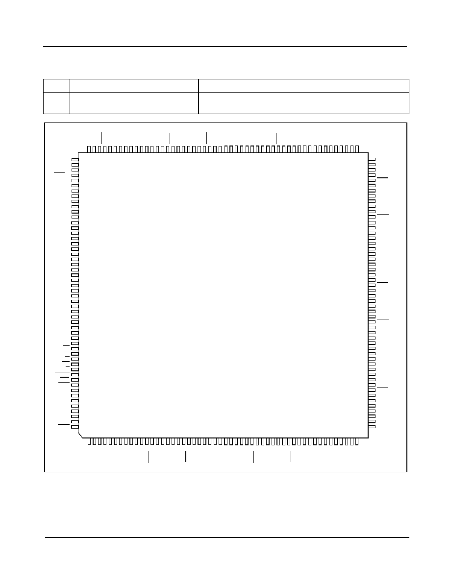
MT9072
Data Sheet
22
Zarlink Semiconductor Inc.
1.0 Change Summary
Figure 2 - Pin Connections (Jedec MS-026)
Page
Item
Change
241
"Recommended Operating
Conditions" Table.
Corrected Min. value to 3.0.
132
134
136
138
140
142
144
146
148
150
152
154
156
22
24
26
168
166
164
162
160
158
20
18
16
14
12
10
8
6
4
2
170
188
186
184
182
180
176
174
172
178
190
208
206
204
202
200
196
194
192
198
VD
D
RP
O
S
[0]
RN
E
G[0
]
E
x
CL
i[0]
TP
O
S
[0]
TN
E
G[0
]
TxC
L
[0]
RxD
L
[0]
RxDL
C[0]
TxD
L
[0]
TxDL
C[0]
Rx
M
F
[0
]
DS
Ti[0]
DS
To
[
0
]
CS
Ti[0]
C
S
T
O
[[0
]
CK
i[0]
FP
i[0]
RxB
F
[0
]
TN
E
G[2
]
RP
O
S
[1]
RN
E
G[1
]
E
x
CL
i[1]
TP
O
S
[1]
TN
E
G[1
]
TRST
TCK
TMS
TDO
TDI
T2
T1
T3
TxMF
TAIS
RESET
I/M
IRQ
R/W
DS
CS
A11
A10
A9
A8
A7
A6
A5
A4
A3
A2
A1
A0
VDD
VSS
D15
D14
D13
D12
D11
D10
D9
D8
D7
D6
D5
D4
D2
D3
D1
D0
VDD
VSS
RxBF[7]
FPi[7]
CKi[7]
CSTo[7]
CS
T
i
[
7
]
DS
T
o
[
7
]
DS
T
i
[
7
]
Rx
M
F
[7
]
T
x
DL
C[
7]
TxD
L
[7
]
Rx
D
L
C[
7]
Rx
D
L
[
7
]
TxC
L
[7
]
TN
E
G[7
]
TP
OS
[
7
]
E
x
CL
i[7]
R
N
E
G[7]
RP
O
S
[
7
]
VD
D
VSS
Rx
B
F
[6]
FP
i[6
]
CK
i
[
6]
CS
T
o
[
6
]
CS
T
i
[
6
]
TxD
L
[6
]
DS
T
i
[
6
]
Rx
M
F
[6
]
TxC
L
[6
]
T
x
DL
C[
6]
208 PIN LQFP
130 128 126 124 122 120 118 116 114 112 110 108 106
32
30
28
94
96
98
100
102
104
34
36
38
40
42
44 46
48
50
52
92
74
76
78
80
82
86
88
90
84
72
54
56
58
60
62
66
68
70
64
RxDL
[1]
RxDL
C[1]
TxDL
[1]
TxDL
C[1]
RxM
F
[1
]
DS
Ti[1]
DS
T
o
[
1
]
CS
Ti[1]
CS
T
o
[
1
]
CK
i[1]
FP
i[1]
RxB
F
[1
]
VS
S
VD
D
R
P
OS[2
]
RNE
G[2]
E2i
[
2
]
TP
OS[2
]
TxCL
[2]
RxDL
[2]
RxDL
C[2]
TxDL
[2]
TxDL
C[2]
RxMF[2]
DSTi[2]
DSTo[2]
CSTi[2]
CSTo[2]
CKi[2]
FPi[2]
RxBF[2]
VSS
VDD
RPOS[3]
RNEG[3]
ExCLii[3]
TPOS[3]
TNEG[3]
TxCL[3]
RxDL[3]
RxDLC[3]
TxDL[3]
TxDLC[3]
RxMF[3]
DSTi[3]
DSTo[3]
CSTi[3]
CSTo[3]
CKi[3]
FPi[3]
RxBF[3]
VSS
VDD
RPOS[4]
RNEG[4]
ExCLi[4]
TPOS[4]
TNEG[4]
TxCL[4]
RxDL[4]
RxDLC[4]
TxDL[4]
TxDLC[4]
RxMF[4]
DSTi[4]
CSTi[4]
DSTo[4]
CSTo[4]
CKi[4]
FPi[4]
RxBF[4]
VSS
VDD
RPOS[5]
RNEG[5]
DS
To
[
6
]
RxD
L
C[6
]
RxD
L
[6]
TNEG[6
]
TPOS
[6]
E
x
CL
i[6]
RN
E
G[6
]
RPOS
[6]
VD
D
VS
S
RxB
F
[5
]
FP
i[5]
CK
i[5
]
CS
To
[
5
]
CS
Ti[5
]
DS
To
[
5
]
DS
Ti[5
]
RxM
F
[5
]
TxDL
C[5
]
TxD
L
[5]
RxD
L
C[5
]
RxD
L
[5]
TxC
L
[5]
TNEG[5
]
TPOS
[5]
E
x
CL
i5]
VS
S
VD
D
TxC
L
[1]
VS
S

MT9072
Data Sheet
23
Zarlink Semiconductor Inc.
Figure 3 - 220 PIN LBGA (Jedec MO-192)
Note: The pin numbers inside the balls for the LBGA package correspond to the pin numbers on the device in the Pin Description
Table.
11
12
13
14
15
16
5
6
7
8
9
10
4
3
2
1
L
M
N
P
R
T
E
F
G
H
J
K
D
C
B
A
NC
207
TCK
101
VSS
NC
4
RNEG[0]
3
RPOS[0]
8
TXCL[0]
7
TNEG[0]
12
TXDLC[0]
11
TXDL[0]
16
CSTI[0]
15
DSTo[0]
20
RXBF[0]
19
FPi[0]
26
TPOS[1]
25
EXCLi[1]
30
RXDLC[1]
29
RXDL[1]
34
DSTI[1]
33
RXMF[1]
35
DSTo[1]
37
CSTOI1]
38
CKI[1]
43
RPOS[2]
44
RNEG[2]
47
TNEG[2]
48
TXCL[2]
51
TXDL[2]
52
TXDLC[2]
18
CKI[0]
55
DSTo[2]
56
CSTI[2]
160
RXBF[7]
159
FPI[7]
166
D3
165
D2
156
CSTI[7]
155
DSTo[7]
NC
209
IDDq
205
TDO
206
TMS
202
T1
204
TDI
201
T3
164
D1
163
D0
158
CKI[7]
154
DSTI[7]
32
TXDLC[1]
161
VSS
58
CKI[2]
53
RXMF[2]
54
DSTI[2]
49
RXDL[2]
57
CSTO[2]
157
CSTO[7]
36
CSTI[1]
45
EXCLi[2]
208
203
T2
5
EXCLi[0]
9
RXDL[0]
17
CSTO[0]
23
RPOS[1]
24
RNEG[1]
31
TXDL[1]
28
TXCL[1]
39
FPi[1]
40
RXBF[1]
153
RXMF[7]
46
TPOS[2]
50
RXDLC[2]
13
RXMF[0]
14
DSTI[0]
141
VSS
6
TPOS[0]
121
VSS
10
RXDLC[0]
27
TNEG[1]
60
RXBF[2]
66
TPOS[3]
70
RXDLC[3]
74
DSTI[3]
76
CSTI[3]
71
TXDL[3]
72
TXDLC[3]
67
TNEG[3]
75
DSTo[3]
63
RPOS[3]
64
RNEG[3]
68
TXCL[3]
77
CSTO[3]
78
CKI[3]
83
RPOS[4]
84
RNEG[4]
87
TNEG[4]
88
TXCL[4]
91
TXDL[4]
92
TXDLC[4]
89
RXDL[4]
85
EXCLi[4]
93
RXMF[ 4]
79
FPI[3]
113
RXMF[5]
114
DSTI[5]
109
RXDL[5]
110
RXDLC[5]
105
EXCLi[5]
106
TPOS[5]
99
FPi[4]
100
RXBF[4]
95
DSTo[4]
96
CSTI[4]
98
CKI[4]
103
RPOS[5]
104
RNEG[5]
107
TNEG[5]
97
CSTO[4]
111
TXDL[5]
115
DSTo[5]
116
CSTI[5]
112
TXDLC[5]
108
TXCL[5]
149
RXDL[7]
145
EXCLi[7]
139
FPI[6]
130
DSTo[6]
138
CKI[6]
137
CSTO[6]
150
RXDLC[7]
146
TPOS[7]
136
CSTI[6]
152
TXDLC[7]
140
RXBF[6]
143
RPOS[7]
151
TXDL[7]
147
TNEG[7]
148
TXCL[7]
144
RNEG[7]
135
TXDL6]
127
TNEG[6]
123
RPOS6]
117
CSTO[5]
120
RXBF[5]
119
FPI[5]
131
TXDLC[6]
132
TXCL6]
118
CKI5]
134
DSTI[6]
124
RNEGI6]
125
EXCLi[6]
133
RXMF[6]
128
RXDL[6]
129
RXDLC[6]
126
TPOS[6]
1
VSS
61
VSS
41
VSS
21
VSS
22
VDD
42
VDD
62
VDD
122
VDD
142
VDD
162
2
VDD
102
VDD
TRST
59
FPI[2]
65
EXCLi[3]
69
RXDL[3]
73
RXMF[3]
90
RXDLC[4]
86
TPOS[4]
94
DSTI[4]
80
RXBF[3]
168
D5
167
D4
169
D6
180
171
D8
172
D9
173
D10
174
177
D14
181
A0
178
D15
182
A1
175
D12
183
A2
187
A6
192
A11
185
A4
186
A5
190
A9
191
A10
193
CS
195
RW
196
IRQ
199
TAIS
200
TXMF
198
RESET
197
194
189
188
184
176
D13
D11
A3
VDD
A8
A7
DS
IM
Top
View
82
VDD
179
VSS
170
D7
81
VSS
VDD
NC
NC
NC
NC
NC
NC
NC
NC

MT9072
Data Sheet
24
Zarlink Semiconductor Inc.
Pin Description
Pin #
Name
Type
Description (see Notes 1 to 7)
LQFP
LBGA
1,21,41,61,
81,101,121,
141,161,
179
E7,E8,E9,
E10,E11,
M7,M8,M9,
M10,M11
V
SS
P
Ground. 0V
DC
.
2,22,42,62,
82,102,122,
142,162,18
0
G5,H5,J5,
K5,L5,G12,
H12J12,K1
2,L12
V
DD
P
Supply Voltage. +3.3 V
DC
nominal.
3
23
43
63
83
103
123
143
D1
H3
N1
N7
P9
R15
K13
F15
RPOS[0]
RPOS[1]
RPOS[2]
RPOS[3]
RPOS[4]
RPOS[5]
RPOS[6]
RPOS[7]
I
Receive Positive. This pin is an input for the receive side of the
framer; it typically interfaces to an LIU. If used by itself it can accept
single rail NRZ (Non Return to Zero) data. If RPOS is used in
conjunction with RNEG it can accept dual rail NRZ data or dual rail RZ
(Return to Zero) data. The clock at the EXCLi pin is used to clock data
into the RPOS pin. Pins RPOS[0-7] are used for Framers[0-7]
respectively.
In T1 mode, transmit line codes are selected with control bits:
RZCS1-0, RXB8ZS, RZNRZ and UNIBI (Address Y01). T1 mode is
selected if the T1E0 bit (Address 900) is 1.
In E1 mode, line codes are selected with control bits: COD0-1 and
RHDB3 at (Address Y02). E1 mode is selected if the T1E0 bit
(Address 900) is 0.
4
24
44
64
84
104
124
144
D2
H4
N2
N8
P10
R16
K14
F16
RNEG[0]
RNEG[1]
RNEG[2]
RNEG[3]
RNEG[4]
RNEG[5]
RNEG[6]
RNEG[7]
I
Receive Negative. This pin is an input for the receive side of the
framer; it typically interfaces to an LIU. RNEG is used in conjunction
with RPOS to accept dual rail NRZ (Non Return to Zero) data or dual
rail RZ (Return to Zero) data. The clock at the EXCLi pin is used to
clock data into the RNEG pin. Pins RNEG[0-7] are used for
Framers[0-7] respectively.
In T1 mode, receive line codes are selected with control bits:
RZCS1-0, RXB8ZS, RZNRZ and UNIBI at (Address Y01). T1 mode is
selected if the T1E0 bit (Address 900) is 1.
In E1 mode, line codes are selected with control bits: COD0-1 and
RHDB3 at (Address Y02). E1 mode is selected if the T1E0 bit
(Address 900) is 0.
5
25
45
65
85
105
125
145
D3
J1
N3
P5
P11
P13
K15
E13
EXCLi(0)
EXCLi(1)
EXCLi(2)
EXCLi(3)
EXCLi(4)
EXCLi(5)
EXCLi(6)
EXCLi(7)
I
1.544/2.048 MHz Extracted Clock. The rising edge of the clock
applied at this input is used to clock RZ data into the receive side of
the framer on pins RPOS and RNEG. If RPOS/RNEG are configured
for NRZ input then either a rising or falling edge on the EXCLi clock
can be selected to clock RPOS/RNEG data. Pins EXCLi[0-7] are used
for Framers[0-7] respectively.
In T1 mode, this pin accepts a 1.544 MHz extracted clock. An active
rising or falling edge is selected with the CLKE bit (Address Y01). See
Figure 53.
In E1 mode, this pin accepts a 2.048 MHz extracted clock. An active
rising or falling edge is selected with the CLKE bit (Address Y02). See
Figure 73.

MT9072
Data Sheet
25
Zarlink Semiconductor Inc.
6
26
46
66
86
106
126
146
D4
J2
N4
P6
P12
P14
K16
E14
TPOS[0]
TPOS[1]
TPOS[2]
TPOS[3]
TPOS[4]
TPOS[5]
TPOS[6]
TPOS[7]
O
Transmit Positive. This pin is an output for the transmit side of the
framer; it typically interfaces to an LIU. If used by itself it can provide
single rail NRZ (Non Return to Zero) data. If TPOS is used in
conjunction with TNEG it can provide dual rail NRZ data or dual rail RZ
(Return to Zero) data. The clock at the TXCL pin is used to clock data
out of the TPOS pin. Pins TPOS[0-7] are used for Framers[0-7]
respectively.
In T1 mode, line codes are selected with control bits: TZCS2-0, TPDV,
TXB8ZS, RZNRZ and UNIBI (Address Y01). T1 mode is selected if the
T1E0 bit (Address 900) is 1.
In E1 mode, line codes are selected with control bits: COD0-1 and
THDB3 (Address Y02). E1 mode is selected if the T1E0 bit (Address
900) is 0.
7
27
47
67
87
107
127
147
E1
J3
P1
P7
R9
P15
J13
E15
TNEG[0]
TNEG[1]
TNEG[2]
TNEG[3]
TNEG[4]
TNEG[5]
TNEG[6]
TNEG[7]
O
Transmit Negative. This pin is an output for the transmit side of the
framer; it typically interfaces to an LIU. TNEG is used in conjunction
with TPOS to provide dual rail NRZ (Non Return to Zero) data or dual
rail RZ (Return to Zero) data. The clock at the TXCL pin is used to
clock data out of the TNEG pin. Pins TNEG[0-7] are used for
Framers[0-7] respectively.
In T1 mode, line codes are selected with control bits: TZCS2-0, TPDV,
TXB8ZS, RZNRZ and UNIBI (Address Y01). T1 mode is selected if the
T1E0 bit (Address 900) is 1.
In E1 mode, line codes are selected with control bits: COD0-1 and
THDB3 (Address Y02). E1 mode is selected if the T1E0 bit (Address
900) is 0.
8
28
48
68
88
108
132
148
E2
J4
P2
P8
R10
P16
J14
E16
TXCL[0]
TXCL[1]
TXCL[2]
TXCL[3]
TXCL[4]
TXCL[5]
TXCL[6]
TXCL[7]
IO 1.544/2.048 MHz Transmit Clock. This pin accepts/outputs a clock
that is used to clock data out of the transmit side of the framer on pins
TPOS and TNEG. If TPOS/TNEG are configured for RZ output then
the rising edge of the clock is used to clock TPOS/TNEG data. If
TPOS/TNEG are configured for NRZ output then either a rising or
falling TxCL edge can be selected to clock TPOS/TNEG data. Pins
TxCL[0-7] are used for Framers[0-7] respectively.
In T1 mode this pin is an input. The 1.544 MHz transmit clock is
typically provided by an external PLL (Phase Lock Loop) or LIU. An
active rising or falling edge is selected with the CLKE bit (Address
Y01). See Figure 52.
In E1 mode this pin is an output. The 2.048 MHz transmit clock is
synchronous with the 4.096 MHz ST-BUS clock input to pin CKi. An
active rising or falling edge is selected with the T2OP bit (Address
Y02). See Figure 71.
Pin Description (continued)
Pin #
Name
Type
Description (see Notes 1 to 7)
LQFP
LBGA

MT9072
Data Sheet
26
Zarlink Semiconductor Inc.
9
29
49
69
89
109
128
149
E3
K1
P3
R5
R11
N13
J15
D13
RxDL[0]
RxDL[1]
RxDL[2]
RxDL[3]
RxDL[4]
RxDL[5]
RxDL[6]
RxDL[7]
O
Receive Data Link. The entire received data stream including framing
bits, after B8ZS/HDB3 decoding, is clocked out of the RxDL pin by the
clock at the EXCLi pin. RxDL data does not pass through the receive
slip buffer. The embedded data link is flagged by RxDLC. Pins
RxDL[0-7] are used for Framers[0-7] respectively.
In T1 mode this is a 1.544 Mbit/s data stream clocked out with the
rising edge of the clock at the EXCLi pin.
In E1 mode this is a 2.048 Mbit/s data stream clocked out with the
falling edge of the clock at the EXCLi pin.
10
30
50
70
90
110
129
150
E4
K2
P4
R6
R12
N14
J16
D14
RxDLC[0]
RxDLC[1]
RxDLC[2]
RxDLC[3]
RxDLC[4]
RxDLC[5]
RxDLC[6]
RxDLC[7]
O
Receive Data Link Clock. This pin outputs a clock that can be used to
clock selected bits from the RxDL data stream into an external device.
The RxDLC pin can also be configured as an enable signal. Pins
RxDLC[0-7] are used for Framers[0-7] respectively.
In T1 mode the FDL (Facility Data Link) bits embedded in the RxDL
data stream can be clocked into an external device with the rising
edge of this 4 kHz clock. The rising edge of the clock is centered on
the S-bit position and it is coincident with the falling edge of the clock
provided to the EXCLi pin. The RxDLC pin can be configured as a
clock or an enable signal with the DLCK bit (Address Y06). See Figure
49.
In T1 IMA (Inverse Mux for ATM) mode the RxDLC pin outputs the
same 1.544 MHz clock that is input to the EXCLi pin. In IMA mode the
DSTo data stream will be synchronous with this 1.544 MHz clock. IMA
mode is selected by setting the IMA bit (Address Y00) to 1. See Figure
39.
In E1 mode the selected data link national bits (timeslot 0, bits 4-8 of
the NFAS (Non-Frame Alignment Signal) frames) can be clocked into
an external device with the rising edge of this clock. The Receive Data
Link clock is a gapped 4, 8, 12, 16 or 20 kHz, clock as programmed by
the Datalink Control Register (Address Y08), derived by gating the
2.048 MHz clock provided to the EXCLi pin. The RxDLC pin can be
configured as a clock or an enable signal with the DLCK bit (Address
Y08). See Figure 68.
In E1 IMA (Inverse Mux for ATM) mode the RxDLC pin provides an
ST-BUS type 4.096 MHz clock derived by doubling the 2.048 MHz
clock provided to the EXCLi pin. In IMA mode the DSTo data stream
will be synchronous with this 4.096 MHz clock. IMA mode is selected
by setting the IMA bit (Address Y00) to 1. See Figure 58.
Pin Description (continued)
Pin #
Name
Type
Description (see Notes 1 to 7)
LQFP
LBGA

MT9072
Data Sheet
27
Zarlink Semiconductor Inc.
11
31
51
71
91
111
135
151
F1
K3
R1
R7
T9
N15
H13
D15
TxDL[0]
TxDL[1]
TxDL[2]
TxDL[3]
TxDL[4]
TxDL[5]
TxDL[6]
TxDL[7]
I
Transmit Data Link. This pin accepts data from an external device for
the Transmit Data Link. Pins TxDL[0-7] are used for Framers[0-7]
respectively.
In T1 mode this pin accepts a 4 kbit/s serial input stream that contains
the ESF FDL (Facility Data Link) bits that are to be embedded in the
transmit data stream. The data is clocked in by the rising edge of the
clock provided at the TxDLC pin. TxDL data does not pass through the
transmit slip buffer.
In E1 mode this pin accepts a 4,8,12,16 or 20 kbit/s, as programmed
by the Datalink Control Register (Address Y08), data stream which
contains the data link national bits (timeslot 0, bits 4-8 of the NFAS
(Non-Frame Alignment Signal) frames) for transmission. The selected
data link national bits are clocked into the framer by the falling edge of
the clock provided at the TxDLC pin.
12
32
52
72
92
112
131
152
F2
K4
R2
R8
T10
N16
H14
D16
TxDLC[0]
TxDLC[1]
TxDLC[2]
TxDLC[3]
TxDLC[4]
TxDLC[5]
TxDLC[6]
TxDLC[7]
O
Transmit Data Link Clock. This pin provides a clock that is used to
clock transmit data link data out of an external device into the TxDL
pin. The TxDLC pin can also be configured as an enable signal. Pins
TxDLC[0-7] are used for Framers[0-7] respectively.
In T1 mode, this pin provides either a 4 kHz clock derived by gating
the 1.544 MHz clock provided to the TxCL pin, or it provides an enable
signal. The TxDLC pin can be configured as a clock or an enable
signal with the DLCK bit (Address Y06). Transmit data link data does
not pass through the transmit slip buffer. See Figure 47.
In E1 mode, this pin provides either a gapped 4,8,12,16 or 20 kHz
clock, as programmed by the Datalink Control Register (Address Y08),
derived by gating the 2.048 MHz clock provided to the TxCL pin, or it
provides an enable signal. The TxDLC pin can be configured as a
clock or an enable signal with the DLCK bit (Address Y08). See Figure
66.
Pin Description (continued)
Pin #
Name
Type
Description (see Notes 1 to 7)
LQFP
LBGA

MT9072
Data Sheet
28
Zarlink Semiconductor Inc.
13
33
53
73
93
113
133
153
F3
L1
R3
T5
T11
M13
H15
C13
RxMF[0]
RxMF[1]
RxMF[2]
RxMF[3]
RxMF[4]
RxMF[5]
RxMF[6]
RxMF[7]
O
Receive Multiframe Boundary. This pin provides a pulse that
identifies basic frame 0 (the start of bit cell 7 of channel 0) of each
received multiframe on the ST-BUS data stream (DSTo). The RxMF
pin operates the same way in 2.048 Mbit/s and 8.196 Mbit/s modes.
Pins RxMF[0-7] are used for Framers[0-7] respectively.
In T1 mode, the RxMF pulse is 244 ns wide and its center identifies
basic frame 0 of the received multiframe. If the Tx8KEN control bit
(Address YF1) is 1 then the RxMF pin outputs an 8kHz frame pulse
synchronous with the data stream on TPOS/TNEG. See Figure 43 and
Figure 45.
In T1 IMA mode, the frame pulse duration is 648 ns.
In E1 mode, (and E1 IMA mode) the RxMF pulse is 244 ns wide and
its center identifies basic frame 0 of the received CAS (Channel
Associated Signaling) multiframe boundary or the received CRC-4
multiframe boundary as determined by the MFSEL control bit
(Address Y02). If the Tx8KEN control bit (Address Y02) is 1 then the
RxMF pin outputs and 8 kHz frame pulse synchronous with the data
stream on TPOS/TNEG. See Figure 62 and Figure 64.
14
94
F4
T12
DSTi[0]
DSTi[4]
I
Data ST-BUS. This pin is an input for the transmit side of the framer. In
2.048 Mbit/s ST-BUS mode and IMA mode it operates the same as
DSTi(1-3), it can also operate in 8.192 Mbit/s ST-BUS mode. IMA
mode is not available at 8.192 Mbit/s. The DSTi data stream is clocked
into the framer by the clock input to pin CKi.
When operated in 8.192 Mbit/s ST-BUS mode this pin accepts a data
stream containing 128 8-bit channels accommodating four framers.
See Table 2 and Table 5. The frame boundary is indicated by the FPi
inputs. Pin DSTi[0] is used by Framers[0-3] and pin DSTi[4] is used by
Framers[4-7].
In 8.192 Mbit/s mode, the 32 ST-BUS channels mapped to each
framer are treated as described for DSTi(1-3) operating at
2.048 Mbit/s.
Pin Description (continued)
Pin #
Name
Type
Description (see Notes 1 to 7)
LQFP
LBGA

MT9072
Data Sheet
29
Zarlink Semiconductor Inc.
34
54
74
114
134
154
L2
R4
T6
M14
H16
C14
DSTi[1]
DSTi[2]
DSTi[3]
DSTi[5]
DSTi[6]
DSTi[7]
I
Data ST-BUS. In 2.048 Mbit/s ST-BUS mode and IMA mode this pin is
an input for the transmit side of the framer. This pin is not used in
8.192 Mbit/s ST-BUS mode. The DSTi data stream is clocked into the
framer by the clock input to pin CKi. Pins DSTi[0-7] are used by
Framers[0-7] respectively.
In T1 mode, this pin accepts a 2.048 Mbit/s ST-BUS stream. The first
24 ST-BUS channels contain the data to be transmitted on the PCM24
interface. See Table 1.
In T1 IMA mode, this pin accepts a 1.544 Mbit/s serial stream that
contains a framing bit followed by the 24 8-bit channels to be
transmitted on the PCM24 interface, see Table 3. The framing bit is
ignored and an internally generated framing bit is used. IMA mode is
selected by setting the IMA bit (Address Y00) to 1.
In E1 mode, this pin accepts a 2.048 Mbit/s ST-BUS stream that
contains the data to be transmitted on the PCM30 interface. See Table
4 and Table 6.
In E1 IMA mode, this pin accepts a 2.048 Mbit/s ST-BUS stream that
contains the data to be transmitted on the PCM30 interface. IMA mode
is selected by setting the IMA bit (Address Y00) to 1. See Table 4 and
Table 6.
15
95
G1
T13
DSTo[0]
DSTo[4]
O
Data ST-BUS. This pin is an output for the receive side of the framer.
In 2.048 Mbit/s ST-BUS mode and IMA mode it operates the same as
DSTo(1-3), it can also operate in 8.192 Mbit/s ST-BUS mode. IMA
mode is not available at 8.192 Mbit/s. The DSTo data stream is
clocked out of the framer by the clock input to pin CKi.
When operated in 8.192 Mbit/s ST-BUS mode this pin outputs a data
stream containing 128 8-bit channels accommodating four framers.
See Table 2 and Table 5. The frame boundary is indicated by the FPi
inputs. Pin DSTo[0] is used by Framers[0-3] and pin DSTo[4] is used
by Framers[4-7].
The 32 ST-BUS channels mapped to each framer are treated as
described for DSTi(1-3) operating at 2.048 Mbit/s.
Pin Description (continued)
Pin #
Name
Type
Description (see Notes 1 to 7)
LQFP
LBGA

MT9072
Data Sheet
30
Zarlink Semiconductor Inc.
35
55
75
115
130
155
L3
T1
T7
M15
G13
C15
DSTo[1]
DSTo[2]
DSTo[3]
DSTo[5]
DSTo[6]
DSTo[7]
O
Data ST-BUS. In 2.048 Mbit/s ST-BUS mode and IMA mode this pin is
an output for the receive side of the framer. This pin is not used in
8.192 Mbit/s ST-BUS mode. Pins DSTo[0-7] are used by Framers[0-7]
respectively.
In T1 mode, this pin outputs 2.048 Mbit/s ST-BUS data. The first 24
channels contain the 24 8-bit channels received on the PCM24
interface. Channel 31 bit 0 contains the received S-bit in D4 and ESF
modes. See Table 1.The DSTo data stream is clocked out of the
framer by the clock input to pin CKi. The DSTo pin is enabled if the
DSToEN control bit (Address YF1) is set to 1.
In T1 IMA mode, this pin outputs the 1.544 Mbit/s received serial
stream. The serial stream contains the framing bit followed by the 24
8-bit channels received on the PCM24 interface. See Table 3. In IMA
mode the DSTo data stream is clocked out of the framer by the clock
output by the RxDLC pin. The DSto pin is enabled if the DSToEN
control bit (Address YF1) is set to 1. IMA mode is selected by setting
the IMA bit (Address Y00) to 1.
In E1 mode, this pin outputs 2.048 Mbit/s ST-BUS data. The 32
channels contain the 32 channels of data received on the PCM30
interface. See Table 4 and Table 6. The DSTo data stream is clocked
out of the framer by the clock input to pin CKi. The DSTo pin is
enabled if the DSToE control bit (Address Y02) is set to 1.
In E1 IMA mode, this pin outputs the 2.048 Mbit/s received serial
stream. See Table 4 and Table 6. In IMA mode the DSTo data stream
is clocked out of the framer by the clock output by the RxDLC pin. The
DSTo pin is enabled if the DSToE control bit (Address Y02) is set to 1.
IMA mode is selected by setting the IMA bit (Address Y00) to 1.
16
96
G2
T14
CSTi[0]
CSTi[4]
I
Control ST-BUS. This pin is the signaling input for the transmit side of
the framer. In 2.048 Mbit/s ST-BUS mode it operates the same as
CSTi(1-3), it can also operate in 8.192 Mbit/s ST-BUS mode. The CSTi
data stream is clocked into the framer by the clock input to pin CKi.
This pin has no function in IMA mode.
When operated in 8.192 Mbit/s ST-BUS mode this pin accepts a data
stream containing 128 8-bit channels accommodating four framers.
See Table 2 and Table 5. The frame boundary is indicated by the FPi
inputs. Pin CSTi[0] is used by Framers[0-3] and pin CSTi[4] is used by
Framers[4-7].
The 32 ST-BUS channels mapped to each framer are treated as
described for CSTi(1-3) operating at 2.048 Mbit/s.
Pin Description (continued)
Pin #
Name
Type
Description (see Notes 1 to 7)
LQFP
LBGA

MT9072
Data Sheet
31
Zarlink Semiconductor Inc.
36
56
76
116
136
156
L4
T2
T8
M16
G14
C16
CSTi[1]
CSTi[2]
CSTi[3]
CSTi[5]
CSTi[6]
CSTi[7]
I
Control ST-BUS. In 2.048 Mbit/s ST-BUS mode this pin is the
signaling input for the transmit side of the framer. This pin has no
function in 8.192 Mbit/s ST-BUS mode or IMA mode. Pins CSTi[0-7]
are used by Framers[0-7] respectively. The CSTi data stream is
clocked into the framer by the clock input to pin CKi.
In T1 robbed bit signaling mode the first 24 ST-BUS channels contain
(XXXXABCD) signaling nibbles to be transmitted for their respective
DS0s. The least significant nibbles (bits 3-0) are valid and the most
significant nibbles of each channel are ignored.
In T1 CCS (Common Channel Signaling) mode, the CSTi pin can be
connected to the output of an external multi-channel HDLC. Any one
of the framer's transmit timeslots can be programmed to transmit the
data appearing at the CSTi pin on any one of the first 24 ST-BUS
channels. See the descriptions of the CSIGEN control bit (Address
Y04) and the Common Channel Signaling Map Register (Address
Y0B).
In E1 CAS (Channel Associated Signaling) mode, the 32 ST-BUS
channels contain (XXXXABCD) signaling nibbles to be transmitted for
their respective timeslots. The least significant nibbles (bits 3-0) are
valid and the most significant nibbles of each channel are ignored.
See Table 25.
In E1 CCS (Common Channel Signaling) mode, the CSTi pin can be
connected to the output of an external multi-channel HDLC. The
framer's transmit timeslots 15, 16 and 31 can each be programmed to
transmit the data appearing at the CSTi pin on any one of the 32
ST-BUS channels. See the descriptions of the CSIG control bit
(Address Y03) and the TS15E, TS16E and TS31E control bits
(Address Y06) and see Table 27.
17
97
G3
T15
CSTo(0)
CSTo[4]
OH Control ST-BUS. This pin is the signaling output for the receive side
of the framer. In 2.048 Mbit/s ST-BUS mode it operates the same as
CSTo(1-3), it can also operate in 8.192 Mbit/s ST-BUS mode. The
CSTo data stream is clocked out of the framer by the clock input to pin
CKi. This pin has no function in IMA mode.
When operated in 8.192 Mbit/s ST-BUS mode this pin outputs a data
stream containing 128 8-bit channels accommodating four framers.
See Table 2 and Table 5. The CSTo[0] pin is used by Framers [0-3]
and the CSTo[4] pin is used by Framers [4-7]. The frame boundary is
indicated by the FPi inputs. FPi[0] is used for Framers[0-3] and FPi[4]
is used for Framers[4-7].
The 32 ST-BUS channels mapped to each framer are treated as
described for CSTo(1-3) operating at 2.048 Mbit/s.
Pin Description (continued)
Pin #
Name
Type
Description (see Notes 1 to 7)
LQFP
LBGA

MT9072
Data Sheet
32
Zarlink Semiconductor Inc.
37
57
77
117
137
157
M1
T3
N9
L13
G15
B13
CSTo[1]
CSTo[2]
CSTo[3]
CSTo[5]
CSTo[6]
CSTo[7]
OH Control ST-BUS. In 2.048 Mbit/s ST-BUS mode this pin is the
signaling output for the receive side of the framer. The CSTo data
stream is clocked out of the framer by the clock input to pin CKi. This
pin has no function in 8.192 Mbit/s ST-BUS mode or IMA mode. Pins
CSTo[0-7] are used by Framers[0-7] respectively.
In T1 robbed bit signaling mode, the first 24 ST-BUS channels contain
(XXXXABCD) signaling nibbles received for their respective DS0s.
The least significant nibbles (bits 3-0) are valid and the most
significant nibbles of each channel are in a high impedance state. The
CSTo pin is enabled if the CSToEN control bit (Address YF1) is set to
1.
In T1 CCS (Common Channel Signaling) mode, the CSTo pin can be
connected to the input of an external multi-channel HDLC. Any one of
the framer's receive timeslots be programmed to output their received
data on the CSTo pin on any one of the first 24 ST-BUS channels.
CSTo is in a high impedance state during unused channels. See the
descriptions of the CSIGEN control bit (Address Y04) and the
Common Channel Signaling Map Register (Address Y0B). The CSTo
pin is enabled if the CSToEN control bit (Address YF1) is set to 1.
In E1 CAS (Channel Associated Signaling) mode, the 32 ST-BUS
channels contain (XXXXABCD) signaling nibbles received for their
respective timeslots. The least significant nibbles (bits 3-0) are valid
and the most significant nibbles of each channel are in a high
impedance state. See Table 26. The CSTo pin is enabled if the CSToE
control bit (Address Y02) is set to 1.
In E1 CCS (Common Channel Signaling) mode, the CSTo pin can be
connected to the input of an external multi-channel HDLC. The
framer's receive timeslots 15, 16 and 31 can each be programmed to
output their received data on the CSTo pin during any one of the 32
ST-BUS channels. CSTo is in a high impedance state during unused
channels. See the descriptions of the CSIG control bit (Address Y03)
and the TS15E, TS16E and TS31E bits (Address Y06) and see
Table 29. The CSTo pin is enabled if the CSToE control bit (Address
Y02) is set to 1.
18
98
G4
T16
CKi[0]
CKi[4]
I
System Clock. In 2.048 Mbit/s ST-BUS mode and 8.192 Mbit/s
ST-BUS mode this pin accepts the clock that is used to time the
transmit side and the receive side of the framer. The CKi clock rate is
determined by control bits at (Address 900)
In 2.048 Mbit/s ST-BUS mode and in IMA mode, operation is the same
as that described for pins CKi[1-3].
In 8.192 Mbit/s ST-BUS mode this pin accepts the ST-BUS type
16.384 MHz clock that is used to time the 8.192 Mbit/s data appearing
at pins DSTi, CSTi, DSTo and CSTo. In this mode pin CKi[0] is used by
framers[0-3] and pin CKi[4] is used by framers[4-7]. See Figure 36.
8.192 Mbit/s operation is not available in IMA mode.
Pin Description (continued)
Pin #
Name
Type
Description (see Notes 1 to 7)
LQFP
LBGA

MT9072
Data Sheet
33
Zarlink Semiconductor Inc.
38
58
78
118
138
158
M2
T4
N10
L14
G16
B14
CKi[1]
CKi[2]
CKi[3]
CKi[5]
CKi[6]
CKi[7]
I
System Clock. In 2.048 Mbit/s ST-BUS mode this pin accepts the
clock that is used to time the transmit side and receive side of the
framer. In IMA mode it accepts the clock that is used to time the
transmit side of the framer only. Pins CKi[0-7] are used to time
Framers[0-7] respectively. The CKi clock rate is determined by control
bits at (Address 900). This pin has no function in 8.192 Mbit/s mode.
In 2.048 Mbit/s ST-BUS mode this pin accepts the ST-BUS type
4.096 MHz clock that is used to time the data appearing at pins DSTi,
CSTi, DSTo and CSTo. See Figure 34.
In T1 IMA mode this pin accepts the 1.544 MHz clock that is used to
time the transmit data appearing at pin DSTi. IMA mode is selected by
setting the IMA bit (Address Y00) to 1. See Figure 40.
In E1 IMA mode this pin accepts the ST-BUS type 4.096 MHz clock
that is used to time the transmit data appearing at pins DSTi. IMA
mode is selected by setting the IMA bit (Address Y00) to 1. In T1/E1
IMA mode the receive data stream is clocked out of pin DSTo by the
clock output by pin RxDLC.
19
99
H1
R13
FPi[0]
FPi[4]
I
Frame Pulse. This pin accepts a frame pulse that sets the basic frame
boundary for the transmit and receive sides of the framer. The clock
rate is determined by control bits at (Address 900)
In 2.048 Mbit/s mode and in IMA mode, operation is the same as that
described for pins FPi[1-3].
In 8.192 Mbit/s mode this pin accepts an 8.192 Mbit/s ST-BUS type
frame pulse which sets the frame boundary common to four framers.
FPi[0] is used to set the frame boundary for Framers[0-3] and FPi[4] is
used to set the frame boundary for Framers[4-7]. See Figure 36.
8.192 Mbit/s operation is not available in IMA mode.
Pin Description (continued)
Pin #
Name
Type
Description (see Notes 1 to 7)
LQFP
LBGA

MT9072
Data Sheet
34
Zarlink Semiconductor Inc.
39
59
79
119
139
159
M3
N5
N11
L15
F13
B15
FPi[1]
FPi[2]
FPi[3]
FPi[5]
FPi[6]
FPi[7]
I
Frame Pulse. This pin accepts a frame pulse that sets the basic frame
boundary for the transmit and receive sides of the framer. In IMA mode
it accepts a frame pulse that sets the basic frame boundary for the
transmit side of the framer only. Pins FPi[0-7] are used to set the frame
boundaries for Framers[0-7] respectively. The clock rate is determined
by control bits at (Address 900). This pin has no function in
8.192 Mbit/s mode.
In 2.048 Mbit/s ST-BUS mode this pin accepts an ST-BUS
2.048 Mbit/s frame pulse that sets the basic frame boundary for the
data that appears at pins DSTi, DSTo, CSTi and CSTo. See Figure 34.
In T1 IMA mode, this pin accepts a 648 ns frame pulse that sets the
basic frame boundary for the transmit data that appears at pin DSTi.
IMA mode is selected by setting the IMA bit (Address Y00) to 1. See
Figure 40.
In E1 IMA mode, this pin accepts a 2.048 Mbit/s ST-BUS type frame
pulse that sets the basic frame boundary for the transmit data that
appears at pin DSTi. IMA mode is selected by setting the IMA bit
(Address Y00) to 1.
In T1 IMA mode and E1 IMA mode, the basic frame boundary for the
receive data stream that is output by DSTo is indicated by the clock
output by the RxBF pin.
20
40
60
80
100
120
140
160
H2
M4
N6
N12
R14
L16
F14
B16
RxBF[0]
RxBF[1]
RxBF[2]
RxBF[3]
RxBF[4]
RxBF[5]
RxBF[6]
RxBF[7]
O
Receive Basic Frame Pulse. This pin outputs a frame pulse that
indicates the basic frame boundary for the received data stream
output by the RxDL pin. In IMA mode the receive basic frame pulse
also indicates the basic frame boundary in the received data stream
output by the DSTo pin. Pins RxBF[0-7] are used to set the frame
boundaries for Framers[0-7] respectively.
In T1 mode, this pin provides a basic frame pulse that indicates the
S-bit in the 1.544 Mbit/s received data stream output by pin RxDL. See
Figure 48.
In T1 IMA mode, the Receive Basic Frame Pulse indicates the S-bit in
the 1.544 Mbit/s received data stream output by pin DSTo. IMA mode
is selected by setting the IMA bit (Address Y00) to 1. See Figure 39.
In E1 mode, this pin provides a 2.048 Mbit/s ST-BUS type frame pulse
that indicates the beginning of channel 0 in the 2.048 Mbit/s received
data stream output by the RxDL pin. See Figure 69.
In E1 IMA mode, the receive basic frame pulse indicates the beginning
of channel 0 in the 2.048 Mbit/s received data stream output by the
DSTo pin. IMA mode is selected by setting the IMA bit (Address Y00)
to 1. See Figure 58.
Pin Description (continued)
Pin #
Name
Type
Description (see Notes 1 to 7)
LQFP
LBGA
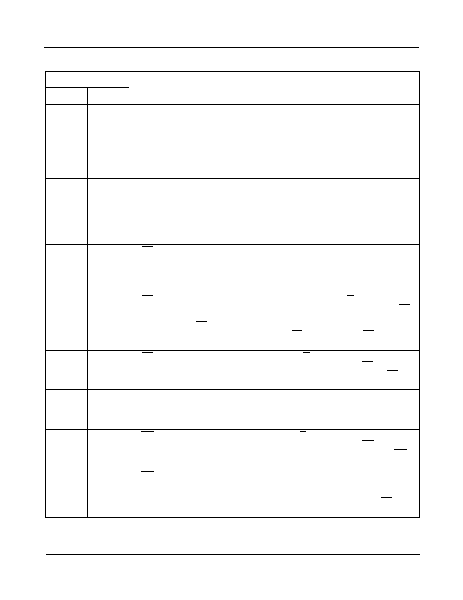
MT9072
Data Sheet
35
Zarlink Semiconductor Inc.
163-178
A13,A14,
A15,A16,
B12,A12,
C12,D12,
A11,B11,
C11,D11,
C10,D10,
B10,A10
D0-D15
I/O Data 0 to 15. These 16 signals form the bidirectional data bus for the
non-multiplexed parallel processor interface. D15 is the most
significant bit.
181-192
B9,A9,C9,
D9,B8,C8,
A8,D8,D7,
B7,C7,A7
A0-A11
I
Address 0 to 11. These 12 signals form the input address bus for the
non-multiplexed parallel processor interface. Bits A10 and A8
determine which of the eight framers is selected for read and write
operations, bit A11 being high and A8 to A10 being low selects all
eight framers for write operations. A11 and A8 being both high and A9
being low selects global control registers. A11 is the most significant
bit.
193
A6
CS
I
Chip Select. A zero enables the read and write functions of the
MT9072 parallel processor interface; all bidirectional data bus lines
(D0-D15) will operate normally. A one disables the read and write
functions of the parallel processor interface; all bidirectional data
bus lines (D0-D15) will be in a high impedance state.
194
D6
DS
I
Data Strobe. Data Strobe for Motorola mode (I/M=0). The MT9072
reads data from the address bus (A0-A11) on the falling edge of DS;
writes data to the bidirectional data bus (D0-D15) on the falling edge
of DS (processor read); reads data from the bidirectional data bus
(D0-D15) on the falling edge of DS (processor write). DS may be
connected to CS.
D6
(RD)
I
Read. Read for Intel type mode (I/M=1). The MT9072 reads data
from the address bus (A0-A11) on the falling edge of RD; writes data
to the bidirectional data bus (D0-D15) on the falling edge of RD
(processor read).
195
B6
R/W
I
Read/Write. Read and Write for Motorola mode (I/M=0). A zero sets
the MT9072 bidirectional data bus lines (D0-D15) as inputs for a
processor write. A one sets the MT9072 bidirectional data bus lines
(D0-D15) as outputs (processor read).
B6
(WR)
I
Write. Write for Intel type mode (I/M=1). The MT9072 reads data
from the address bus (A0-A11) on the falling edge of WR; reads data
from the bidirectional data bus (D0-D15) on the rising edge of WR
(processor write).
196
C6
IRQ
OH Interrupt Request. When zero, one or more of the eight framers in the
MT9072 has generated an interrupt request. When one, the MT9072
has not generated an interrupt request. IRQ is an open drain output
that should be connected to V
DD
through a pull-up resistor. CS can be
either high or low for this output pin to function.
Pin Description (continued)
Pin #
Name
Type
Description (see Notes 1 to 7)
LQFP
LBGA

MT9072
Data Sheet
36
Zarlink Semiconductor Inc.
197
D5
IM
I
Intel / Motorola. High configures the processor interface for Intel type
of parallel non-multiplexed processors where RD and WR pins are
used. Low configures the processor interface for Motorola type of
parallel non-multiplexed processors where R/W and DS pins are used.
See Figure 28 and Figure 29.
198
C5
RESET
I
Reset. When zero, all eight framers of the MT9072 are in a reset
condition where all registers are set to their default values. When one,
all eight framers of the MT9072 operate normally where all registers
may be programmed by the external processor. A valid reset condition
requires this input to be held low for a minimum of 100 ns. This input
should be set to zero during initial power up, then set to one.
199
A5
TAIS
I
Transmit Alarm Indication Signal. When zero, all eight framers of
the MT9072 transmit an all ones signal (AIS) at the TPOS and TNEG
output pins. When one, all eight framers of the MT9072 transmit data
normally. This input is typically set to zero during initial power up, then
set to one.
200
B5
TxMF
I
Transmit Multiframe Boundary. This pin accepts a frame pulse that
sets the multiframe boundary for the framer transmitters. The device
will generate its own multiframe boundary if this pin is held high. The
TxMF pin is held high in most applications. This input is common for all
eight framers, and is enabled on a per framer basis with a control
register bit. Operation is identical in 2.048 Mbit/s and 8.192 Mbit/s
modes.
In T1 mode the frame pulse applied to this pin sets the transmitted
D4/ESF multiframe boundary. The falling edge of this frame pulse
identifies basic frame 0 on the ST-BUS data stream (DSTi). This input
is enable with control bit TxMFSEL (Address YF1). See Figure 41.
In E1 mode the frame pulse applied to this pin sets the transmitted
channel associated signaling (CAS) multiframe boundary or the
transmitted CRC-4 multiframe boundary. The falling edge of this frame
pulse identifies basic frame 0 on the ST-BUS data stream (DSTi) of the
16 frame multiframe. This input is enabled with control bit MFBE
(Address Y02). See Figure 60.
201
A4
RSV
--
This pin should be tied low.
202
B4
RSV
--
This pin should be tied low.
203
C4
RSV
--
This pin should be tied low.
204
A3
TDI
IPu Test Data Input. One of five signals (TDI, TDO, TMS, TCK & TRST)
making up the Test Access Port (TAP) of the IEEE 1149.1-1990
Standard Test Port and Boundary-Scan Architecture. The TAP
provides access to test support functions built into the MT9072. The
TAP is also referred to as a JTAG (Joint Test Action Group) port.
Pin Description (continued)
Pin #
Name
Type
Description (see Notes 1 to 7)
LQFP
LBGA

MT9072
Data Sheet
37
Zarlink Semiconductor Inc.
205
A2
TDO
OH Test Data Output. Depending on the sequence previously applied to
the TMS input, the contents of either the instruction register or data
register are serially shifted out towards the TDO. The data out of the
TDO is clocked on the falling edge of the TCK pulses. When no data is
shifted through the boundary scan cells, the TDO driver is set to a high
impedance state. See the pin description for TDI and the section on
JTAG.
206
B3
TMS
IPu Test Mode Select Input. The logic signals received at the TMS input
are interpreted by the TAP Controller to control the test operations.
The TMS signals are sampled at the rising edge of the TCK pulse.
Internally pulled up to V
DD
. See the pin description for TDI and the
section on JTAG.
207
B2
TCK
IPu Test Clock Input. TCK provides the clock for the test logic. The TCK
does not interfere with any on-chip clocks and thus remains
independent. The TCK permits shifting of test data into or out of the
Boundary-Scan register cells concurrently with the operation of the
device and without interfering with the on-chip logic. Internally pulled
up to V
DD
. See the pin description for TDI and the section on JTAG.
See Figure 30.
208
C3
TRST
IPu Test Reset. When zero, the JTAG scan structure is reset. When one,
the JTAG scan structure operates normally. Internally pulled up to
V
DD
. See the pin description for TDI and the section on JTAG. A valid
device reset condition requires this input to be held low for a minimum
of 100 ns. This input is should be set to zero during initial power up,
then set to one if the JTAG port is to be used, otherwise, it may be
permanently set to zero.
--
B1
RSV
--
This pin should be tied low.
Notes:
1.
All inputs are CMOS with CMOS compatible logic levels.
2.
All unused inputs should be tied low.
3.
All outputs are CMOS and are compatible with CMOS logic levels.
4.
See AC Electrical Characteristics - Timing Parameter Measurement Voltage Levels for input and output voltage thresholds.
5.
The number enclosed in parentheses following the pin name identifies the framer as follows:
[0] - framer 0, [1] - framer 1, [2] - framer 2,... [7] - framer 7
6.
The "Y" character in the register address symbolizes the upper 4 address bits (A
11
A
10
A
9
A
8
) which identify the particular framer addressed
within the MT9072 as follows:
[0] 0000 - framer 0, [1] 0001 - framer 1,... [2] 0010 - framer 2,... [7] 0111 - framer 7
[8] 1000 - all 8 framers.
7.
Pin types are as follows:
I
- input (5 V tolerant input
IP
- input with a pullup or pulldown, these are 3 V tolerant inputs.
O
- output
I/O
- input and output
OH
- output and high impedance
OD
- output open drain
Pin Description (continued)
Pin #
Name
Type
Description (see Notes 1 to 7)
LQFP
LBGA

MT9072
Data Sheet
38
Zarlink Semiconductor Inc.
2.0 Overview
The MT9072 is an eight port (octal) framing device that can be software configured for T1, E1 or J1 operation. Each
of the eight framers can be independently timed and controlled. Each framer features one embedded HDLC
(High-level Data Link Controller) that can be assigned to the maintenance channel or to any other channel.
2.1 Standards Compliance
In T1 mode, the MT9072 meets or supports the latest recommendations including AT&T PUB43801, TR-62411,
ANSI T1.102, T1.403 and T1.408. It also supports Telcordia GR-303-CORE. In T1 ESF mode the CRC-6
calculation and yellow alarm can be configured to meet the requirements of a J1 interface.
In E1 mode, the MT9072 meets or supports the latest ITU-T Recommendations for PCM30 and ISDN primary rate
including G.703, G.704, G.706, G.732, G.775, G.796, G.823, G.965 (V5.2) and I.431. It also meets or supports ETSI
TBR4, TBR13, ETS 300 233, and ETS 300 347 (V5.2).
2.2 Microprocessor Port
A 16-bit parallel Motorola or Intel non-multiplexed microprocessor interface is used to access the control and status
registers.
2.3 Interface to the Physical Layer Device
On the line side the MT9072 framers interface to physical layer devices (typically LIUs) using a Return to Zero (RZ)
or Non Return to Zero (NRZ) protocol. The data can be single rail or dual rail with several T1 and E1 line coding
options available.
In T1 mode, the receive and transmit paths each include a two-frame slip buffer. The transmit slip buffer features
programmable delay and it serves as a rate converter between the ST-BUS and the 1.544 Mbit/s T1 line rate.
In E1 mode, the receive path includes a two-frame slip buffer.
2.4 Interface to the System Backplane
On the system side the MT9072 framers can interface to a 2.048 Mbit/s or 8.192 Mbit/s ST-BUS backplane, or a
2.048 Mbit/s GCI backplane.
There is an IMA (Inverse MUX for ATM) mode for IMA applications, this enables the framer to interface to a
1.544 Mbit/s (T1) or 2.048 Mbit/s (E1) serial bus with asynchronous transmit and receive timing.
2.5 Framing Modes
The MT9072 framers operate in termination mode or transparent mode. In the receive transparent mode, the
received line data is channelled to the DSTo pin with arbitrary frame alignment. In the transmit transparent mode,
no framing or signaling is imposed on the data transmitted from the DSTi pin onto the line.
In T1 mode the framers operate in any of the following framing modes: D4, Extended Superframe (ESF) or T1DM.
In E1 mode the framers run three framing algorithms: basic frame alignment, signalling multiframe alignment and
CRC-4 multiframe alignment. The Remote Alarm Indication (RAI) bit is automatically controlled by an internal state
machine.

MT9072
Data Sheet
39
Zarlink Semiconductor Inc.
2.6 Access to the Maintenance Channel
The T1 ESF Facility Data Link (FDL) bits can be accessed in the following three ways: Through the data link pins
TxDL, RxDL, RxDLC and TxDLC or through internal registers for Bit Oriented Messages or through the embedded
HDLC.
In E1 mode the Sa bits (bits 4-8 of the non-frame alignment signal) can be accessed in four ways: Through data
link pins TxDL, RxDL, RxDLC and TxDLC or through single byte transmit and receive registers or through five
byte transmit and receive national bit buffers or through the embedded HDLC.
2.7 Robbed Bit Signaling/Channel Associated Signaling
Robbed bit signaling and channel associated signaling information can be accessed two ways: Via the microport;
via the CSTi and CSTo pins. Signaling information is frozen upon loss of multiframe alignment.
In T1 mode the MT9072 supports AB and ABCD robbed bit signaling. Robbed bit signaling can be enabled on a
channel by channel basis.
In E1 mode the MT9072 supports Channel Associated Signaling (CAS) multiframing.
2.8 Common Channel Signaling
MT9072 supports Common Channel Signaling (CCS) with the embedded HDLCs and with the capability to map
external HDLCs to/from the transmit/receive timeslots.
In T1 mode CCS is supported in any one channel by using the embedded HDLC. Alternatively, the CSTi and CSTo
pins can be used to map an external HDLC channel to/from any one transmit/receive T1 channel.
In E1 mode CCS is supported in any one timeslot by using the embedded HDLC. Alternatively, the CSTi and CSTo
pins can be used to map three external HDLC channels to/from any of transmit/receive E1 timeslots 15, 16 and 31.
2.9 HDLCs
The MT9072 provides one embedded HDLC per framer with 32 byte deep transmit and receive FIFOs.
In T1 mode the embedded HDLC can be assigned to the FDL or any channel. It can operate at 4 kbit/s (Data Link),
56 kbit/s or 64 kbit/s.
In E1 mode the embedded HDLC can be assigned to timeslot zero Sa bits (bits 4-8 of the non-frame alignment
signal), or any other timeslot. It can operate at 4, 8, 12, 16, 20 (Data Link) or 64 kbit/s.
2.10 Performance Monitoring and Debugging
The MT9072 has a comprehensive suite of performance monitoring and debugging features. These include error
counters, loopbacks, deliberate error insertion and a 2
15
�1 QRS/PRBS generator/detector.
2.11 Interrupts
The MT9072 provides a comprehensive set of maskable interrupts. Interrupt sources consist of synchronization
status, alarm status, counter indication and overflow, timer status, slip indication, maintenance functions and
receive signaling bit changes.
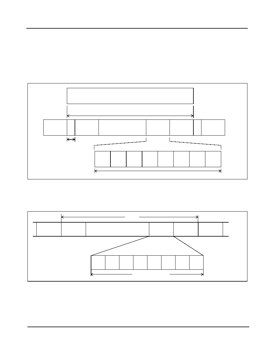
MT9072
Data Sheet
40
Zarlink Semiconductor Inc.
3.0 PCM24 Interface (T1)
3.1 T1 Interface to the System Backplane
PCM24 (T1) basic frames are 193 bits long and are transmitted at a frame repetition rate of 8000 Hz, which results
in an aggregate bit rate of 193 bits x 8000/sec =1.544 Mbits/sec. Basic frames are divided into 24 channels
numbered 1 to 24 and a framing bit; see Figure 4. Each timeslot is 8 bits in length and is transmitted most
significant bit first (numbered bit 1). This results in a single channel data rate of 8 bits x 8000/sec. = 64 kbit/s.
Figure 4 - PCM24 Link Frame Format (T1)
It should be noted that the Zarlink ST-BUS has 32 channels numbered 0 to 31 and the most significant bit of an
eight bit channel is numbered bit 7, see Figure 5. Therefore, ST-BUS bit 7 is synonymous with DS0 bit 1; bit 6 with
bit 2 and so on. See Zarlink Application note MSAN-126 for more details on the ST-BUS.
Figure 5 - ST-BUS Format
In the case of mapping ST-BUS to the PCM24 payload, only the first 24 channels and the last channel (31) of an
ST-BUS are used (see Table 1). Timeslot 31 S-bit is only used if TXSYNC bit Y00 is set. All unused channels are
tristate.
DS1 FRAME
(8/1.544) us
CHANNEL
1
BIT 1
BIT 2
BIT 3
BIT 4
BIT 5
BIT 6
BIT 7
BIT 8
CHANNEL
24
CHANNEL
23
CHANNEL
1
S
BIT
S
BIT
CHANNEL
24
125 us
(1/1.544) us
� � � � � � � � �
CHANNEL
31 or 127
0
30 or 126
BIT
CHANNEL
CHANNEL
CHANNEL
CHANNEL
31 or 127
0
BIT
BIT
BIT
BIT
BIT
BIT
BIT
� � �
Least
Significant
Bit (Last)
Most
Significant
Bit (First)
125
�s
7
6
5
4
3
2
1
0
(8/2.048 or 8/8.192)
�s

MT9072
Data Sheet
41
Zarlink Semiconductor Inc.
The relationship between DSTi/CSTi and the voice channels in 8.192 Mbit/s mode is shown in Table 2 (F01-F7 refer
to the Framer numbers). There are 2 multiplexed streams (DSTi/o0 and CSTi/o0 are used to multiplexed data for
Framers 0 to 3 and DSTi/o4 and CSTi/o4 is used for framers 5 to 7).
When the device is in IMA (Inverse Mux for ATM) mode, the mapping is the S-bit followed by 24 PCM channels.
This relationship is shown in Table 3. Note that the S-bit location in the Table is indicated by the bit number; which
starts from bit 0. Hence the strict definition of ST-BUS channels is not adhered to. As in a T1 interface the data on
the DSTi/o is a bit followed by 24 channels.
When signaling information is written to the MT9072 using ST-BUS control links (as opposed to direct writes by the
microport to the on-board signaling registers), the CSTi channels corresponding to the selected DSTi channel
streams are used to transmit the signaling bits. Since the maximum number of signaling bits associated with any
channel is 4 (in the case of ABCD), only half a CSTi (bits 3 to 0) channel is required for sourcing the signaling bits.
Bit A is bit 3 from the CSTi stream, Bit B is 2, Bit C is 1 and Bit D is 0. Unused channels and unused bits are tristate.
In T1 transparent mode, the DSTi data is transparently sent to the PCM24 channels. In transparent mode the data
on the DSTi streams will appear unaltered on the PCM24 links and data received on the PCM24 link will pass
unaltered to the DSTo streams. No signaling insertion or extraction is done in transparent mode. If the TxSYNC
control bit (address Y00) is 1 then the transmit S-bit is overwritten by channel 31 bit 0 in the 2.048 Mbit/s ST-BUS
mode. In the 8.192 Mbit/s ST-BUS mode the S-bits from channels 124, 125, 126, 127 respectively are used to
override the transmit S-bit positions for Framers 0 to 3 or 4 to 7 respectively. If T1 Transparent mode and IMA mode
are both selected then the S-bit and channel bits are transparently mapped as shown in Table 3.
PCM24 Channels
1
2
3
4
5
6
7
8
9
10
11
12
13
14
15
16
ST-BUS Channels
(DSTi/o and CSTi/o)
0
1
2
3
4
5
6
7
7
9
10
11
12
13
14
15
PCM24 Channels
17
18
19
20
21
22
23
24
-
-
-
-
-
-
-
S-bit
ST-BUS Channels
(DSTi/o and CSTi/o)
16
17
18
19
20
21
22
23
24
x
25
x
26
x
27
x
28
x
29
x
30
x
31
Table 1 - ST-BUS vs. PCM24 Channel Relationship for 2.048 Mbit/s DST/CST Streams (T1)
PCM24 Channels
1
2
3
4
5
6
7
8
9
10
11
12
13
14
15
16
ST-BUS
F0/4
Chan(DSTi/o
F1/5
and CSTi/o)
F2/6
F3/7
0
1
2
3
4
5
6
7
8
9
10
11
12
13
14
15
16
17
18
19
20
21
22
23
24
25
26
27
28
29
30
31
32
33
34
35
36
37
38
39
40
41
42
43
44
45
46
47
48
49
50
51
52
53
54
55
56
57
58
59
60
61
62
63
PCM24 Channels
17
18
19
20
21
22
23
24
S-bit
-
-
-
-
-
-
-
ST-BUS
F0/4
Chan(DSTi/o
F1/5
and CSTi/o)
F2/6
F3/7
64
65
66
67
68
69
70
71
72
73
74
75
76
77
78
79
80
81
82
83
84
85
86
87
88
89
90
91
92
93
94
95
124
125
126
127
Table 2 - ST-BUS Channel vs. PCM24 Channel Relationship for 8.192 Mbit/s DST/CST Streams (T1)

MT9072
Data Sheet
42
Zarlink Semiconductor Inc.
3.2 T1 Interface to the Physical Layer Device
Control bits in the Line Interface and Coding word (address Y01) determine the format of the PCM24 transmit and
receive signals. Three physical interface formats are provided including RZ dual rail, NRZ dual rail and NRZ single
rail.
The detailed timing diagrams are presented in Figures 45 to Figures 48.
RZ Dual Rail - On the Transmit side the pulse width is approximately half the duration of the PCM24 bit cell
centered around the falling edge of TXCL. On the receive side RPOS and RNEG are sampled on the falling edge of
EXCLi. Note that the CLKE bit in register Y01 (selectable for edge sampling) has no effect in RZ mode.
NRZ Dual Rail - With this format, pulses are present for the full bit cell, which allows the set-up and hold times to be
easily met. For the receiver the sampling point can be the rising edge or the falling edge of the EXCLi clock,
depending on the CLKE bit in Register Y01. The transmitted data can be output either on the rising or falling edge
of TXCL selected by the CLKE bit. TXCL is an input in T1 mode and an output in E1 mode.
NRZ Single Rail - This NRZ format is not dual rail, and therefore, only requires a single output line and a single
input line (i.e., TPOS and RPOS). The CLKE bit in Register Y01 controls the TXCL clock edge and the EXCLi
sampling edge.
3.3 T1 Line Coding
B8ZS (zero code substitution) is selectable globally for both the transmit and receive path (register Y01). Jammed
bit 7, GTE, DDS or BELL zero code suppression are also available for the transmitter and receiver(register Y01).
Different schemes for provision of ones density can be selected with bits ZCS2:0 (registers Y01). GTE suppression
is achieved by replacing the LSB of zero bytes by a one except for the signaling frame. DDS suppression is
replacement of zero byte by 10011000. Bell code suppression is replacement of bit 1(second bit after LSB) of a
zero byte. Jammed bit seven selection will replace the LSB of each channel with a '1'.
3.4 T1 Pulse Density
Bit 4 of address Y10 (PDV) toggles if the receive data fails to meet ones density requirements. It will toggle upon
detection of 16 consecutive zeros in the line data, or if there are fewer than N ones in a window of 8(N+1) bits -
where N = 1 to 23.
The transmit T1 data is monitored and if the 12.5% density requirement is not met over a maximum 192 bit window
a one is inserted in a non-framing bit. The window and PDV criteria is the same as the received PDV.
PCM24 Channels
S
bit
1
2
3
4
5
6
7
8
9
10
11
12
13
14
15
ST-BUS Channels
(DSTi/o)
Bit
0
0
1
2
3
4
5
6
7
8
9
10
11
12
13
14
PCM24 Channels
16
17
18
19
20
21
22
23
24
ST-BUS Channels
(DSTi/o)
15
16
17
18
19
20
21
22
23
Table 3 - ST-BUS vs. PCM24 to Channel Relationship for IMA DST Streams (T1)

MT9072
Data Sheet
43
Zarlink Semiconductor Inc.
4.0 PCM30 Interface (E1)
4.1 E1 Interface to the System Backplane
PCM30 (E1) basic frames are 256 bits long and are transmitted at a frame repetition rate of 8000 Hz, which results
in an aggregate bit rate of 256 bits x 8000/sec = 2.048 Mbits/sec. The actual bit rate is 2.048 Mbit/s +/-50 ppm
encoded in HDB3 (High Density Bipolar 3) format. Basic frames are divided into 32 timeslots numbered 0 to 31, see
Figure 6. Each timeslot is 8 bits in length and is transmitted most significant bit first (numbered bit 1). This results in
a single timeslot data rate of 8 bits x 8000/sec. = 64 kbit/s.
It should be noted that the Zarlink ST-BUS also has 32 channels numbered 0 to 31, but the most significant bit of an
eight bit channel is numbered bit 7, see Figure 5. Therefore, ST-BUS bit 7 is synonymous with PCM30 bit 1; bit 6
with bit 2: and so on, see Zarlink Application Note MSAN-126 for more details on the ST-BUS.
Tables 4 and 5 show the mapping between the ST-BUS channels and the PCM30 timeslots.
When the device is in IMA (Inverse Mux for ATM) mode the mapping between the ST-BUS Channels and the
PCM30 timeslots is according to Table 4.
PCM30 timeslot 0 is reserved for basic frame alignment, CRC-4 multiframe alignment and the communication of
maintenance information (facility data link). In most configurations timeslot 16 is reserved for either Channel
Associated Signaling (CAS or ABCD bit signaling) or Common Channel Signaling (CCS). For V5.2 applications,
timeslots 15, 16 and 31 may be used for CCS. The remaining timeslots are called channels and carry either PCM
encoded voice signals or digital data. Channel alignment and bit numbering is consistent with timeslot alignment
and bit numbering. However, channels are numbered 1 to 30 and relate to timeslots as per Table 6.
PCM30 Timeslots
0
1
2
3
4
5
6
7
8
9
10
11
12
13
14
15
ST-BUS Channels
(DSTi/o and CSTi/o)
0
1
2
3
4
5
6
7
8
9
10
11
12
13
14
15
PCM30 Timeslots
16
17
18
19
20
21
22
23
24
25
26
27
28
29
30
31
ST-BUS Channels
(DSTi/o and CSTi/o)
16
17
18
19
20
21
22
23
24
25
26
27
28
29
30
31
Table 4 - ST-BUS Channel vs. PCM30 Timeslot for 2.048 Mbit/s DST/CST Streams (E1)
PCM30 Timeslots
0
1
2
3
4
5
6
7
8
9
10
11
12
13
14
15
ST-BUS
F0/4
Chan(DSTi/o F1/5
and CSTi/o) F2/6
F3/7
0
1
2
3
4
5
6
7
8
9
10
11
12
13
14
15
16
17
18
19
20
21
22
23
24
25
26
27
28
29
30
31
32
33
34
35
36
37
38
39
40
41
42
43
44
45
46
47
48
49
50
51
52
53
54
55
56
57
58
59
60
61
62
63
PCM30 Timeslots
16
17
18
19
20
21
22
23
24
25
26
27
28
29
30
31
ST-BUS
F0/4
Chan(DSTi/o F1/5
and CSTi/o) F2/6
F3/7
64
65
66
67
68
69
70
71
72
73
74
75
76
77
78
79
80
81
82
83
84
85
86
87
88
89
90
91
92
93
94
95
96
97
98
99
100
101
102
103
104
105
106
107
108
109
110
111
112
113
114
115
116
117
118
119
120
121
122
123
124
125
126
127
Table 5 - ST-BUS Channel vs. PCM30 Timeslot Relationship for 8.192 Mbit/s DST/CST Streams (E1)

MT9072
Data Sheet
44
Zarlink Semiconductor Inc.
Figure 6 - PCM30 Format (E1)
4.2 E1 Interface to the Physical Layer Device
Register control bits COD1-0 (address Y02) determine the format of the PCM30 transmit and receive signals. Three
interface formats are provided including RZ dual rail, NRZ dual rail and NRZ single rail.
RZ Dual Rail - On the Transmit side the pulse width is approximately half the duration of the PCM30 bit cell
centered around the falling edge of TXCL. On the receive side RPOS and RNEG are sampled on the falling edge of
EXCLi. Note that the T2OP bit in Register Y02 (selectable for edge sampling) has no effect in RZ mode.
NRZ Dual Rail - With this format, pulses are present for the full bit cell, which allows the set-up and hold times to be
easily met. For the receiver the sampling point can be the rising edge or the falling edge of the EXCLi clock
dependent on the CLKE bit in Register Y01. The transmitted data can be output either on the rising or falling edge
of TXCL selected by the T2OP bit. TXCL is an input in T1 mode and output in E1 mode.
NRZ Single Rail - This NRZ format is not dual rail, and therefore, only requires a single output line and a single
input line (i.e., TPOS and RPOS). The T2OP bit controls the TXCL clock edge and CLKE bit controls the
RPOS/RNEG sampling.
HDB3 - Register Control bit THDB3 (address Y02) determines the PCM30 encoding in the transmit direction. The
encoding can either be HDB3 or alternate mark inversion (AMI). The RHDB3 (address Y02) bit selects the receive
HDB3 decoding.
PCM30 Timeslot
0
1 2 3...15
16
17 18 19...31
PCM30 Voice/Data
Channels
x
1 2 3...15
x
16 17 18...30
Table 6 - PCM30 Timeslot to PCM30 Channel Relationship (E1)
FRAME
15
0
14
15
0
TIMESLOT
0
1
30
31
Most
Significant
Bit (First)
Least
Significant
Bit (Last)
BIT
1
2
3
4
5
6
7
8
FRAME
FRAME
FRAME
FRAME
TIMESLOT
TIMESLOT
TIMESLOT
BIT
BIT
BIT
BIT
BIT
BIT
BIT
2.0 ms
(8/2.048)
�s
125
�s
� � � � � � � �
� � � �

MT9072
Data Sheet
45
Zarlink Semiconductor Inc.
5.0 Framing
5.1 T1 Framing
DS1 trunks contain 24 bytes of serial voice/data channels bundled with an overhead bit - the S-bit. The S-bit
contains a fixed repeating pattern used to enable DS1 receivers to delineate frame boundaries. S-bits are inserted
once per frame at the beginning of the transmit frame boundary. The DS1 frames are further grouped in bundles of
frames, generally 12 (for D4 applications) or 24 frames deep (for ESF - extended superframe applications). The
registers for controlling and observing the framing algorithms are presented in the Table 7.
Register
Address
Register
Description
Y00
Framing Mode Select
This register is used for selecting the different framing modes
from ESF to D4 or T1DM. The register is also used for selecting
reframe criteria.
Y10
Synchronization and Alarm
Status Word.
This register provides the real time status of the receive framing
algorithm as to basic frame synchronization and multiframe
synchronization.
Y16
MFOOF Counter
This status register increments every 1.5 msec for D4 mode or
every 3 msec for ESF mode when the basic frame
synchronization is lost.
Y17
Framing Bit Error Counter
This counter counts the Ft errors in ESF mode and Ft+Fs error in
D4 and T1DM.
Y19
CRC-6 Error Counter
This counter counts the CRC-6 errors by comparing the
calculated CRC-6 with the CRC-6 bits in the ESF frame.
Y1A
Out of Frame Counter and
Change of Frame Counter
The out of frame counter is incremeted with every loss of receive
frame synchronization. The change of frame counter is
incremented with every shift in the frame alignment position.
Y24
Receive Sync and Alarm Latch
This register contains latched bits for events related to framing
such as framing bit errors.
Y28
Framing Bit Error Count Latch
This counter is a latched version of Y17, the value of this counter
is updated every 1 sec.
Y2A
CRC-6 Error Counter Latch
This counter is a latched version of Y19, the value of this counter
is updated ever 1 sec.
Y2B
Out of Frame Counter Latch and
Change of Frame Counter Latch
This counter is a latched version of Y19, the value of this counter
is updated ever 1 sec.
Y2C
MFOOF Counter Latch
This counter is a latched version of Y16, the value of this counter
is updated ever 1 sec.
Y34
Receive Sync Interrupt Status
Register
This register captures interrupt events related to the receiver
framer such as Framing Bit error. Interrupts can be generated by
setting appropriate masks.
Y44
Receive Sync Interrupt Status
Register Mask
This mask corresponds to the Y34 status register. Writing a "0"
unmasks an interrupt.
Table 7 - Registers Related to Framing Mode for the MT9072 (T1)

MT9072
Data Sheet
46
Zarlink Semiconductor Inc.
5.1.1 T1 D4 Framing
For D4 links the S-bit position contains an alternating 101010... pattern inserted into every second S-bit. These bits
are intended for determination of frame boundaries, and they are referred to as Ft bits. A separate fixed pattern,
repeating every superframe, is interleaved with the Ft bits. This fixed pattern (001110) is used to delineate the 12
frame superframe. These bits are referred to as the Fs bits. In D4 frames # 6 and #12, the LSB of each channel
byte may be replaced with A bit (frame #6) and B bit (frame #12) signaling information. See Table 8.
5.1.2 T1 ESF Framing
For ESF links the 6 bit framing pattern 001011, inserted into every 4th S-bit position, is used to delineate both frame
and superframe boundaries. Frames #6, 12, 18 and 24 may contain the A, B, C and D signaling bits, respectively. A
4 kHz data link is embedded in the S-bit position, interleaved between the framing pattern sequence (FPS) and the
transmit CRC-6 remainder (from the calculation done on the previous superframe). See Table 9.
Frame #
Ft
Fs
Signaling
1
1
2
0
3
0
4
0
5
1
6
1
A
7
0
8
1
9
1
10
1
11
0
12
0
B
Table 8 - D4 Superframe Structure (T1)
Frame #
FPS
FDL
CRC
Signaling
1
X
2
CB1
3
X
4
0
5
X
6
CB2
A
7
X
Table 9 - ESF Superframe Structure (T1)

MT9072
Data Sheet
47
Zarlink Semiconductor Inc.
5.1.3 T1 T1DM Framing
The Ft and Fs bits are identical to the D4 format, channel 24 of each frame has a synchronization byte consisting of
10111YR0.
Y is used to indicate a yellow alarm and is active low. R bit is reserved by AT&T as an 8 Kb/s communication
channel.
The synchronization is first declared if the Ft bit is in sync and subsequently 6 consecutive T1DM synchronization
bytes are received. The synchronization error criteria for the receiver will be the same as D4 (i.e., 2 out of 4, 5 or 6).
Although an error is detected if any of 5 synchronization bits or the Ft/Fs bits are incorrect.The OOF error selection
criteria of 2 errors out of 4, 5, 6 bits is also applicable to the T1DM sync byte format; the error criteria applies to the
synchronization byte and the framing bit. The received sync byte can be monitored by the status register(Y10). The
Y bit an be sent by writing to control register (address Y02). The TIDMR bit can only be input from the Transmit
Data Link Pin. The registers and bits used for T1DM are indicated in the register bit functions.
5.1.4 T1 G.802 Mode
G.802 mode allows interworking between an E1 and T1 system. The line is operating in T1 mode and the
backplane consists of E1 data. The mapping for the backplane channels to the PCM24 side is as shown Table 10.
The 193 bits from the E1 backplane stream are mapped to the 193 bits of the PCM24 side. The channel 0 and
channel 16 on the backplane side are the G.704 Timeslot 0 and 16 channels and are not mapped.
8
0
9
X
10
CB3
11
X
12
1
B
13
X
14
CB4
15
X
16
0
17
X
18
CB5
C
19
X
20
1
21
X
22
CB6
23
X
24
1
D
Frame #
FPS
FDL
CRC
Signaling
Table 9 - ESF Superframe Structure (T1)

MT9072
Data Sheet
48
Zarlink Semiconductor Inc.
5.2 E1 Framing
The following Table shows the registers related to the E1 framing algorithm.
DSTi/DSTo
Channel#, Bit#
PCM24 bits
Function
0
Not mapped
Timeslot 0
1, bit 7(MSB)
S-bit
S-bit
1(bit 6 to 0)-15
119 bits
16
Not mapped
Timeslot 16
17-25
120 to 192
channel 16, bit 1
193 bit
last bit
Table 10 - G.802 ST-BUS to PCM24 Mapping (T1)
Register
Address
Register
Description
Y00
Alarm and Framing Control
Register
This is the main register for selection of the framing mode. The
specific bits for control of the framer are CSYN, AUTY, CRCM,
REFRM, MFRF and AUTC
Y10
Synchronization and Alarm
Status Word.
This register provides the real time status of receive basic frame
synchronization and receive multiframe synchronization. All bits in
this status register are relevant to framing except the slip bits.
Y11
CRC-4 Timers and CRC-4 Local
Status
All bits except the 2 sec timer are related to the reception of the
CRC-4 pattern in timeslot 0.
Y12
Alarm and Multiframe signaling
Status
This register reports alarms such as AIS, loss of signal and
Timeslot 16 and 0 remote alarms. The bits of relevance for
framing are KLVE, LOSS,AIS16, AIS,RAI,RMA1 to 4, Y bit.
Y13
NFAS and FAS Status Register
This register shows the FAS and NFAS status such as RFA 2 to 8
and RNFA.
Y16
Loss of basic frame
synchronization counter
This counter increments by one every 125 usec when the BSYNC
status is set to 1.
Y19
CRC-4 Error Counter
This error counter is incremented for each calculated CRC-4
submultiframe error. The CRCS1 and CRCS2 (Y11 bit 1 and 2)
events increment this counter.
Y1A
FAS Bit Counter and FAS Error
Counter.
This register reflects the FAS bit errors and a combined FAS
pattern error.
Y24
Sync,CRC-4,MAS Latched
Status Register
This register represents the latched version of framing status bits
such as BSYNC. These bits are set by changes in the associated
real time bits.
Table 11 - Registers Related to Framing for MT9072 (E1)

MT9072
Data Sheet
49
Zarlink Semiconductor Inc.
5.2.1 E1 Basic Framing (Timeslot 0)
Timeslot 0 of every 125 us frame is reserved for basic frame alignment and contains a Frame Alignment Signal
(FAS) or a Non-Frame Alignment Signal (NFAS). FAS and NFAS occur in consecutive basic frames as shown in
Table 12.
Bit one of the FAS can be either a CRC-4 remainder bit or an international usage bit.
Bit one of the NFAS can be either a CRC-4 multiframe alignment signal, an E-bit or an international usage bit. Refer
to national standards bodies for specific requirements.
Bit two of the FAS and NFAS is used to distinguish between FAS (bit two = 0) and NFAS (bit two = 1) frames.
Bits two to eight of the FAS are used for basic frame alignment. Basic frame alignment is initiated by a search for
the bit sequence 0011011 which appears in the last seven bit positions of the FAS, see the Frame Algorithm
section.
Bit three of the NFAS (designated as "A"), the Remote Alarm Indication (RAI), is used to indicate the near end basic
frame synchronization status to the far end of a link. Under normal operation, the A (RAI) bit should be set to 0,
while in alarm condition, it is set to 1.
Bits four to eight of the NFAS (i.e., Sa4-8) are additional spare bits which may be used as follows:
� Sa4-8 may be used in specific point-to-point applications (e.g., transcoder equipments conforming to G.761)
� Sa4 may be used as a message-based data link for operations, maintenance and performance monitoring
� Sa5-Sa8 are for national usage but are also available from the Data link interface(TxDL,RxDL)
� Note that for simplicity all Sa bits including Sa4 are collectively called national bits throughout this document.
See the Data Link section for accessing the national bits.
Y27
Performance Presistent Latched
Status Register
This register latches the detection of loss(LOSSP) and basic
frame sync(BSYNCP).
Y2A
CRC-4 Error Counter Latch.
This a a sampled version of Y19 latched every one sec.
Y34
Sync, CRC-4
Remote,Alarm,MAS and Phase
Status Register
These are the interrupt status bits for BSYNC, Receive Multiframe
Alignment Interrupt etc.
Y35
Counter Indication and Counter
Overflow Interrupt status
This register represents the interrupt status bits for counter
overflows, counter indications etc.
Y44
Sync Interrupt Mask Register
This is the mask register for the events in register Y34.
Y45
Counter Indication and Counter
Overflow Interrupt Mask
Register
This is the mask register for the events in register Y35.
Register
Address
Register
Description
Table 11 - Registers Related to Framing for MT9072 (E1)

MT9072
Data Sheet
50
Zarlink Semiconductor Inc.
5.2.2 E1 CRC-4 Multiframing (Timeslot 0)
The primary purpose for CRC-4 multiframing is to provide a verification of the current basic frame alignment,
although it can also be used for other functions such as bit error rate estimation. The CRC-4 multiframe consists of
16 basic frames numbered 0 to 15, and has a repetition rate of 16 frames X 125 microseconds/frame = 2 msec.
CRC-4 multiframe alignment is based on the 001011 bit sequence, which appears in bit position one of the first six
NFASs of a CRC-4 multiframe.
The CRC-4 multiframe is divided into two submultiframes, numbered 1 and 2, which are each eight basic frames or
2048 bits in length.
The CRC-4 frame alignment verification functions as follows. Initially, the CRC-4 operation must be activated and
CRC-4 multiframe alignment must be achieved at both ends of the link. At the local end of a link, all the bits of every
transmit submultiframe are passed through a CRC-4 polynomial (multiplied by X
4
then divided by X
4
+ X + 1), which
generates a four bit remainder. This remainder is inserted in bit position one of the four FASs of the following
submultiframe before it is transmitted (see Table 12).
CRC-4
CRC-4
Frame/Type
PCM30 Channel Zero
1
2
3
4
5
6
7
8
Sub Multi Frame 1
0/FAS
C
1
0
0
1
1
0
1
1
1/NFAS
0
1
A
S
a4
S
a5
S
a6
S
a7
S
a8
2/FAS
C
2
0
0
1
1
0
1
1
3/NFAS
0
1
A
S
a4
S
a5
S
a6
S
a7
S
a8
4/FAS
C
3
0
0
1
1
0
1
1
5/NFAS
1
1
A
S
a4
S
a5
S
a6
S
a7
S
a8
6/FAS
C
4
0
0
1
1
0
1
1
7/NFAS
0
1
A
S
a4
S
a5
S
a6
S
a7
S
a8
Sub Mult
i Fr
ame 2
8/FAS
C
1
0
0
1
1
0
1
1
9/NFAS
1
1
A
S
a4
S
a5
S
a6
S
a7
S
a8
10/FAS
C
2
0
0
1
1
0
1
1
11/NFAS
1
1
A
S
a4
S
a5
S
a6
S
a7
S
a8
12/FAS
C
3
0
0
1
1
0
1
1
13/NFAS
E
1
1
A
S
a4
S
a5
S
a6
S
a7
S
a8
14/FAS
C
4
0
0
1
1
0
1
1
15/NFAS
E
2
1
A
S
a4
S
a5
S
a6
S
a7
S
a8
Table 12 - CRC-4 FAS and NFAS Structure (E1)
indicates position of CRC-4
multiframe alignment signal.

MT9072
Data Sheet
51
Zarlink Semiconductor Inc.
The submultiframe is then transmitted and, at the far end, the same process occurs. That is, a CRC-4 remainder is
generated for each received submultiframe. These bits are compared with the bits received in position one of the
four FASs of the next received submultiframe. This process takes place in both directions of transmission.
When more than 914 CRC-4 errors (out of a possible 1000) are counted in a one second interval, the framing
algorithm will force a search for a new basic frame alignment if automatic CRC-4 interworking is not invoked.
The result of the comparison of the received CRC-4 remainder with the locally generated remainder will be
transported to the far end by the E-bits. Therefore, if E
1
= 0, a CRC-4 error was discovered in a submultiframe 1
received at the far end; and if E
2
= 0, a CRC-4 error was discovered in a submultiframe 2 received at the far end.
No submultiframe sequence numbers or re-transmission capabilities are supported with layer 1 PCM30 protocol.
See ITU-T G.704 and G.706 for more details on the operation of CRC-4 and E-bits.
5.2.2.1 E1 Automatic CRC-4 Interworking
When control bit AUTC (register address Y00) is set to zero, the MT9072 framing algorithm supports automatic
interworking of interfaces with and without CRC-4 processing capabilities. That is, if an interface with CRC-4
capability, achieves valid basic frame alignment, but does not achieve CRC-4 multiframe alignment by the end of a
predefined period, the distant end is considered to be a non-CRC-4 interface. When the distant end is a non-CRC-4
interface, the near end automatically suspends receive CRC-4 functions, continues to transmit CRC-4 data to the
distant end with its E-bits set to zero, and provides a status indication. Naturally, if the distant end initially achieves
CRC-4 synchronization, CRC-4 processing will be carried out by both ends.
When control bit AUTC is one, Automatic CRC-4 Interworking is deactivated. In this case, if the Automatic Remote
Alarm Indication (RAI) Operation (ARAI) control bit (register address Y00) is low, and if CRC-4 multiframe
alignment is not found in 400 msec, then the transmit Remote Alarm Indication (RAI) (bit 3 (A) of the transmit
NFAS) will be continuously high until CRC-4 multiframe alignment is achieved.
The TE control bit (register address Y00) for transmit E bits will have the same function in both states of AUTC.
That is, when CRC-4 synchronization is not achieved the state of the transmit E-bits will be the same as the state of
the TE control bit. When CRC-4 synchronization is achieved the transmit E-bits will function as per ITU-T G.704 as
described in the previous section. Table 13 outlines the operation of the AUTC, ARAI and TALM control bits of the
MT9072.

MT9072
Data Sheet
52
Zarlink Semiconductor Inc.
5.2.3 E1 Channel Associated Signaling (CAS) Multiframing (Timeslot 16)
Refer to the section on Channel Associated Signaling (CAS) Operation.
5.2.4 E1 Framing Algorithm
The MT9072 contains three distinct framing algorithms: basic frame alignment, signaling multiframe alignment and
CRC-4 multiframe alignment. Figure 7 is a state diagram that illustrates these algorithms and how they interact.
After power-up, the basic frame alignment framer will search for a frame alignment signal (FAS) in the PCM30
receive bit stream. Once the FAS is detected, the corresponding bit 2 of the non-frame alignment signal (NFAS) is
checked. If bit 2 of the NFAS is zero a new search for basic frame alignment is initiated. If bit 2 of the NFAS is one
and the next FAS is correct, the algorithm declares that basic frame synchronization has been found (status
register
address Y10
bit BSYNC is reset to zero).
Once basic frame alignment is acquired the signaling and CRC-4 multiframe searches will be initiated. The
signaling multiframe algorithm will align to the first multiframe alignment signal pattern (MFAS = 0000) it receives in
the most significant nibble of channel 16 (status register address Y10 bit MSYNC is zero). Signaling multiframe
alignment will be lost when two consecutive multiframes are received in error.
The CRC-4 multiframe alignment signal is a 001011 bit sequence that appears in PCM30 bit position one of the
NFAS in frames 1, 3, 5, 7, 9 and 11 (see Table 12). In order to achieved CRC-4 synchronization two consecutive
CRC-4 multiframe alignment signals must be received without error (status register address Y10 bit CSYNC is
zero).
The MT9072 framing algorithm supports automatic interworking of interfaces with and without CRC-4 processing
capabilities. That is, if an interface with CRC-4 capability, achieves valid basic frame alignment, but does not
AUTC
ARAI
TALM
Description
0
0
X
Automatic CRC-interworking is activated. If no valid CRC MFAS is being
received, transmit RAI will flicker high with every reframe (8 msec), this cycle
will continue for 400 msec., then transmit RAI will be low continuously. The
device will stop searching for CRC MFAS, continue to transmit CRC-4
remainders, stop CRC-4 processing, indicate CRC-to-non-CRC operation and
transmit E-bits to be the same state as the TE control bit (control register
address Y00).
0
1
0
Automatic CRC-interworking is activated. Transmit RAI is low continuously.
0
1
1
Automatic CRC-interworking is activated. Transmit RAI is high
continuously.
1
0
X
Automatic RAI is activated. Automatic CRC-interworking is de-activated. If
no valid CRC MFAS is being received, transmit RAI flickers high with every
reframe (8 msec), this cycle continues for 400 msec, then transmit RAI
becomes high continuously. The device continues to search for CRC MFAS
and transmit E-bits are the same state as the TE control bit. When CSYN = 0,
the CRC MFAS search is terminated and the transmit RAI goes low.
1
1
0
Automatic RAI is activated. Automatic CRC-interworking is de-activated.
Transmit RAI is low continuously.
1
1
1
Automatic RAI is activated. Automatic CRC-interworking is de-activated.
Transmit RAI is high continuously.
Table 13 - Operation of AUTC, ARAI and TALM Control Bits (E1)

MT9072
Data Sheet
53
Zarlink Semiconductor Inc.
achieve CRC-4 multiframe alignment by the end of a predefined period, the distant end is considered to be a
non-CRC-4 interface. When the distant end is a non-CRC-4 interface, the near end automatically suspends receive
CRC-4 functions, continues to transmit CRC-4 data to the distant end with its E-bits set to zero, and provides a
status indication. Naturally, if the distant end initially achieves CRC-4 synchronization, CRC-4 processing will be
carried out by both ends. This feature is selected when control bit AUTC (control register address Y00) is set to
zero.
5.2.4.1 Notes for Synchronization State Diagram (Figure 7)
1. The basic frame alignment, signaling multiframe alignment, and CRC-4 multiframe alignment functions operate
in parallel and are independent.
2. The receive channel associated signaling bits and signaling multiframe alignment bit will be frozen when multi-
frame alignment is lost.
3. Manual re-framing of the receive basic frame alignment and signaling multiframe alignment functions can be
performed at any time.
4. The transmit RAI bit will be one until basic frame alignment is established, then it will be zero.
5. E-bits can be optionally set to zero until the equipment interworking relationship is established. When this has
been determined one of the following will take place:
a) CRC-to-non-CRC operation - E-bits = 0,
b) CRC-to-CRC operation - E-bits as per G.704 and I.431.
6. All manual re-frames and new basic frame alignment searches start after the current frame alignment signal
position.
7. After basic frame alignment has been achieved, loss of frame alignment will occur any time three consecutive
incorrect basic frame alignment signals are received. Loss of basic frame alignment will reset the complete
framing algorithm.
8. When CRC-4 multiframe alignment has been achieved, the primary basic frame alignment and resulting multi-
frame alignment will be adjusted to the basic frame alignment determined during CRC-4 synchronization. There-
fore, the primary basic frame alignment will not be updated during the CRC-4 multiframe alignment search, but
will be updated when the CRC-4 multiframe alignment search is complete.

MT9072
Data Sheet
54
Zarlink Semiconductor Inc.
Figure 7 - Synchronization State Diagram (E1)
6.0 Elastic Buffer
The MT9072 has a two frame receive elastic (or slip) buffer, which absorbs wander and low frequency jitter in
multi-trunk applications. If desired, the elastic buffer can be bypassed by using the Data Link RxDL pin output (see
the following section). The received data (RPOS and RNEG) is clocked into the elastic buffer with the extracted
(EXCLi pin) clock and is clocked out of the elastic buffer with the system (CKi pin) clock. The EXCLi clock is
generated from the receive data, and is therefore phase-locked with that data. In normal operation, the EXCLi clock
400 msec timer expired
>914 CRC errors
in one second
NO
3 consecutive incorrect
frame alignment
signals
YES
CRC-to-non-CRC interworking. Maintain
primary basic frame alignment. Continue
to send CRC-4 data, but stop CRC
processing. E-bits set to `0'. Indicate
CRC-to-non-CRC operation. Note 7.
Search for primary basic
frame alignment signal
RAI=1, Es=0.
Out of synchronization
Verify Bit 2 of non-frame
alignment signal.
Parallel search for new basic
frame alignment signal.
Notes 6 & 7.
YES
YES
NO
CRC multiframe
alignment
* only if CRC-4 synchronization is selected and
automatic CRC-4 interworking is de-selected.
** only if automatic CRC-4 interworking is selected.
8 msec. timer
expired**
CRC-to-CRC interworking. Re-align to new
basic frame alignment. Start CRC-4
processing. E-bits set as per G.704 and
I.431. Indicate CRC synchronization
achieved.
Notes 7 & 8.
signaling multi-frame
alignment
Primary basic frame
synchronization acquired. Enable
traffic RAI=0, E's=0. Start loss of
primary basic frame alignment
checking. Notes 7 & 8.
YES
CRC-4 multi-frame
alignment
YES
Verify second
occurrence of frame
alignment signal.
Start 8 msec timer.
Note 7.
Multiframe synchronization
acquired as per G.732.
Note 7.
Find two CRC frame
alignment signals.
Note 7.
Check for two consecutive errored
multiframe alignment signals.
Notes 7 & 8.
Start 400 msec timer.
Note 7.
Search for multiframe
alignment signal.
Note 7.
NO
NO
NO
YES
Basic frame
alignment acquired
No CRC
multiframe
alignment.
No CRC multiframe
alignment.
8 msec. timer
expired*
RAI = 0

MT9072
Data Sheet
55
Zarlink Semiconductor Inc.
will be phase-locked to the CKi clock by an external phase locked loop (PLL). Therefore, in a single trunk system,
the receive data is in phase with the EXCLi clock, the CKi clock is phase-locked to the EXCLi clock, and the read
and write positions of the elastic buffer will remain fixed with respect to each other.
In a multi-trunk slave or loop-timed system (i.e., PABX application) a single trunk will be chosen as a network
synchronizer, which will function as described in the previous paragraph. The remaining trunks will use the system
timing derived from the synchronizer to clock data out of their slip buffers. Even though the signals from the network
are synchronous to each other, due to multiplexing, transmission impairments and route diversity, these signals
may jitter or wander with respect to the synchronizing trunk signal. Therefore, the EXCLi clocks of non-synchronizer
trunks may wander with respect to the EXCLi clock of the synchronizer and the system bus.
Network standards state that, within limits, trunk interfaces must be able to receive error-free data in the presence
of jitter and wander (refer to network requirements for jitter and wander tolerance). The MT9072 will allow a
maximum of 26 channels (208 UI, unit intervals) of wander and low frequency jitter before a frame slip will occur.
The minimum delay through the receive slip buffer is approximately two channels and the maximum delay is
approximately 60 channels (see Figure 8).
When the CKi and the EXCLi clocks are not phase-locked, the rate at which data is being written into the slip buffer
from the line side may differ from the rate at which it is being read out onto the ST-BUS. If this situation persists, the
delay limits stated in the previous paragraph will be violated and the slip buffer will perform a controlled frame slip.
That is, the buffer pointers will be automatically adjusted so that a full frame is either repeated or lost. All frame slips
occur on frame boundaries.
Two status bits, RSLP and RSLPD (register address Y10 for E1 and Y13 for T1), give indication of a slip occurrence
and direction. RSLP changes state in the event of a slip. If RSLPD=0, the slip buffer has overflowed and a frame
was lost; if RSLPD=1, a underflow condition occurred and a frame was repeated. A maskable interrupt status bit
RSLIPI (register address Y34 for E1 and Y36 for T1) is also provided.
Figure 8 illustrates the relationship between the read and write pointers of the receive slip buffer. Measuring
clockwise from the write pointer, if the read pointer comes within two channels of the write pointer a frame slip will
occur, which will put the read pointer 34 channels from the write pointer. Conversely, if the read pointer moves more
than 60 channels from the write pointer, a slip will occur, which will put the read pointer 28 channels from the write
pointer. This provides a worst case hysteresis of 13 channels peak (26 channels peak-to-peak) or a wander
tolerance of 208 UI. The registers relevant to controlling and observing the elastic buffer in T1 mode are shown in
Table 14. The registers related to elastic buffer for E1 are shown in Table 15.
Figure 8 - Read and Write Pointers in the Slip Buffers
Write Pointer
60 CH
2 CH
47 CH
15 CH
34 CH
28 CH
512 Bit
Elastic
Store
13 CH
-13 CH
Wander Tolerance
Read Pointer
Read Pointer
Read Pointer
Read Pointer
26
Cha
n
n
e
l
s

MT9072
Data Sheet
56
Zarlink Semiconductor Inc.
In T1 mode, the transmit and receive elastic buffers also serve the purpose of rate conversion between the
1.544 Mbit/s line rate and the 2.048 Mbit/s backplane rate. Consequently, in T1 mode the elastic buffers cannot be
bypassed, except for the special case of T1 IMA mode.
Register
Address
Register
Description
Y00
Framing Mode Select
If IMA mode is selected the transmit and receive elastic buffers
are bypassed.
Y13
Receive Slip Buffer Status Word
This register provides status bits for receive slip and its direction
word that indicates the phase difference between the ST-BUS
and the PCM24
Y14
Transmit Slip Buffer Status Word This register provides status bit for transmit slip and its direction
word that indicates the phase difference between the ST-BUS
and the PCM24.
Y26
Elastic Store and Excessive Zero
Status Latch
This register indicates the latched version of the slip indicator
bits from registers Y13 and Y14.
Y36
Elastic Store and Excessive Zero
Interrupt Status
Interrupt status word for the slip indicators.
Y46
Elastic Store and Excessive Zero
Interrupt Mask
Interrupt mask bits for the slip indicators.
YF7
Transmit Set Delay Bits
This register sets a one time delay through the transmit slip
buffer.
Table 14 - Registers Related to the Elastic Buffer (T1)
Register
Address
Register
Description
Y00
Framing Mode Select
If IMA mode is selected the receive elastic buffers are bypassed.
Y03
DL,CCS,CAS and Other
Control Register
ELAS bit is used to bypass the elastic store, that data at DSTo is
the received. PCM30 data after the HDB3 coding.
Y10
Sync and CRC-4 Remote
status
RSLP and RSLPD show the slip and the direction of the slip.
Y14
Phase Status Indicator
This word reflects the delay through the receive elastic store
from the line to the ST-BUS side.
Y34
Sync,CRC-4 Remote, Alarm,
MAS and Phase Status Word
RSLIPI in this register reflects the interrupt due to a slip.
Y44
Sync,CRC-4 Remote, Alarm,
MAS and Phase Status Word
Interrupt Mask
Interrupt mask bits for the slip indicator.
Table 15 - Registers Related to Elastic Store (E1)

MT9072
Data Sheet
57
Zarlink Semiconductor Inc.
6.1 Transmit Elastic Buffer
In T1 mode, the MT9072 contains a transmit elastic buffer in addition to the receive elastic buffer. Data is clocked
into the transmit elastic buffer by the 2.048 Mbit/s or 8.192 Mbit/s ST-BUS clock (which is subsequently divided to a
2.048 MHz clock). The data is clocked out of the transmit elastic buffer by the 1.544 MHz clock input to the TXCL
pin.
The delay through the transmit elastic buffer will vary in accordance with the position of the channel in the frame.
For example, PCM24 channel 1 sits in the elastic buffer for approximately 1 usec, and PCM24 channel 24 sits in the
elastic buffer for approximately 32 usec. The relative phase delay between the system ST-BUS frame boundary
and the transmit elastic frame read boundary is measured every frame and reported in the Transmit Slip Buffer
Status Word (Y14). In addition, the relative delay between these frame boundaries may be programmed by writing
to Tx Set Delay Bits (register address YF7). Every write to the TX Set Delay Bits resets the Transmit Slip Buffer
MSB bit TxSBMSB (register address Y14). After a write, the delay through the slip buffer is less than 1 frame in
duration. Each write operation will result in a disturbance of the transmit PCM24 frame boundary, causing the far
end to go out of sync.
The transmit elastic buffer is capable of performing controlled slips in a manner similar to the receive elastic buffer.
Slips on the transmit side are independent of slips on the receive side. The two status bits. TSLIP and TSLPD
(register address Y14), give indication of a slip occurrence and direction. TSLP changes state in the event of a slip.
If TSLPD=0, the slip buffer has overflowed and a frame was lost; if TSLPD=1, an underflow condition occurred and
a frame was repeated. A maskable interrupt status bit TXSLIPI (register address Y36) is also provided. Under
normal operation no slips should occur in the transmit path. Slips will only occur if the input CKi clock has excess
wander relative to the input TXCL clock, or if the TX Set Delay Bits (register address YF7) register is initialized too
close to the slip pointers after system initialization.
7.0 Data Link
7.1 T1 Data Link
The ESF protocol allows for carrier messages to be embedded in the S-bit position. The MT9072 provides 3
separate means of controlling the Data Link.
� Transmit and receive Data Link pins TxDL, TxDLC, RxDL and RxDLC.
� Bit - Oriented Messages may be transmit and received via dedicated transmit and receive
registers(Y07,Y08,Y12). This is only applicable in the ESF mode.
� The ESF Data Link (DL) can be connected to an internal HDLC, operating at a bit rate of 4 kbits/sec. The
HDLC can be activated by setting the control bit 1(HDLCEn) of the HDLC & Data Link Control Word (Y06).
In the D4 mode the Fs bits can be inserted/extracted from the Data Link pins by setting the EDLEN bit in Y06. The
registers related to the Data Link are shown in Table 16.

MT9072
Data Sheet
58
Zarlink Semiconductor Inc.
7.1.1 T1 Data Link (DL) Pin Access
When EDLEN(Y06) is set to "1"
the data link (DL) bits can be sourced/sinked to and from the TxDL and RxDL pins,
by enabling the corresponding pulses in either gapped clocks or enable low signals provided at the RxDLC and
TxDLC pins. The option of either gapped clock or enable signal is selected by control bit DLCK (Register address
Y06).
In D4 or ESF mode, the optional serial data link operates at 4 khz. In D4 mode the data link pins are used to
send/receive Fs bits only, while the Ft bits are generated internally. See Figures 40 to 43.
7.1.1.1 T1 Data Link (DL) Pin Data Received from PCM24
The RxDLC clock is derived from the receive extracted clock (EXCLi).The B8ZS decoded receive data, at
1.544 Mbit/s, is clocked out of the device on the RxDL pin with the rising edge of EXCLi and is aligned to RXDLC. In
order to facilitate the attachment of this data stream to a Data Link controller, the clock signal RxDLC (falling edge
of EXCLi) consists of positive pulses, of nominal width of 344 ns, during the Fs bit cell times that are selected for the
Data Link, with the rising edge aligned with the middle of the bit cell. DL data will not be lost or repeated when a
receive frame slip occurs as the DL data does not pass through the elastic buffer. See Figures 42 to 43 for timing
requirements.
7.1.1.2 T1 Data Link (DL) Pin Data Sent to PCM24
The TxDLC clock is derived from the transmit clock (TXCL) and is provided one frame before its usage on the
appropriate S-bit. Hence the TXDLC clock is provided one frame before it is used in ESF Mode in Frames 2, 4, 6, 8,
10, 12, 14, 16, 18, 20, 22, 24. See Figures 40 to 41 for timing requirements.
Register
Address
Register
Description
Y06
HDLC and Data Link Control
Register
This register determines the source of the Data Link which can be
the HDLC, Bit Oriented messages or the external Data Link. This
register also controls the type of clocks provided to the external
Data Link interface.
Y07
Transmit bit Oriented Message This register holds the message that will be sent in ESF FDL if the
BOMEN bit in Y06 is set.
Y08
Receive bit Oriented Message
Match
This register is the match register for received bit oriented message
Y12
Receive bit Oriented Message This register holds the value of the receive bit oriented message
Y25
Receive Line Status and Timer
Latch
This register contains bit oriented message and bit oriented
message match latch bits.
Y35
Receive Line and Timer
Interrupt Status
This register contains bit oriented message and bit oriented
message match interrupt status bits.
Y45
Receive Line and Timer
Interrupt Mask
These are the mask bits for Y35.
Table 16 - Registers Related to the Data Link and Bit Oriented Messages (T1)

MT9072
Data Sheet
59
Zarlink Semiconductor Inc.
7.2 E1 Data Link (DL) Operation
Table 12 shows the contents of the transmit and receive Frame Alignment Signals (FAS) and Non-frame Alignment
Signals (NFAS) of timeslot zero of a PCM30 signal. Even numbered frames (CRC Frame # 0, 2, 4,...) are FASs and
odd numbered frames (CRC Frame # 1, 3, 5,...) are NFASs. The bits of each channel are numbered 1 to 8, with bit
1 being the most significant and bit 8 the least significant. The Data Link (DL) bits, also referred to as National bits,
are the Sa4, Sa5, Sa6, Sa7 and Sa8 bits of the PCM30 timeslot zero NFAS frames. Any number and combination
of these bits may be used for the transport of maintenance and performance monitoring information across the
PCM30 link. The DataLink in controlled by the address Y06 and Y08.
The received Data Link bits are always sent to the DataLink Pins and the National bit buffers(YC0-YC4).
The Data Link (DL) bits (S
a4
~S
a8
) of the PCM30 timeslot zero NFAS frames can be accessed by the MT9072 in the
following four ways:
� External serial port pins. Hence the user can use pins (TxDL and TxDLC) for transmit data link access and
RxDL and RXDLC for receive data link access
� Micro port access which would use Transmit 5 bit register (TNU4-8 address YB0 to YB4). For the receiver
Receive 5 bit register (RNU4-8 address YC0-YC4).
� ST-BUS access Transmit ST-BUS (DSTi timeslot 0) enabled by transparent mode
� On board HDLC for Timeslot 0
Note: that the user can source different Sa bits from a combination of the above 4 methods. For instance the Sa
4
bit could be sourced from the External Serial Port and Sa
5
to Sa
8
from the micro port register (TNU5-8 address YB1
to YB4).
The registers related to the configuration control and status of the data link are shown in Table 17.
Register
Address
Register
Description
Y00
Alarm and Framing Control
Register
The Data Link is not supported in the IMA mode.
Y06
HDLC and CCS ST-BUS
control register
The bit HPSEL has to be 0 if the internal HDLC is to be used for the
Data Link.
Y08
Data Link Control Register
This register determines the source of the Sa bits which can be micro
port,HDLC, data link pins or ST-BUS. This register is also used to
control the data link pins Txdl and Rxdl.
Y13
NFAS and FAS status
The national use bits RNU can be read from this status register.
Y26
CAS, National, CRC-4
Latched Status
The Sa bit latched values can be read from this register, SA5VL,
SA6NL etc.
Y36
CAS, National, CRC-4
Interrupt Status
The Sa bit interrupt values can be read from this register, SA5VI,
SA6NI etc.
Y46
CAS, National, CRC-4
Interrupt Mask
These are the mask bits for Y36.
YB0-YB4 Transmit National Bits
Transmit national bits used for sending
Sa bits(SA4 to SA8).
YC0-YC4 Receive national bit
Receive National bits(SA4 to SA8)
Table 17 - Data Link and Sa Bits Configuration and Status Registers (E1)

MT9072
Data Sheet
60
Zarlink Semiconductor Inc.
7.2.1 E1 Data Link (DL) Pin Access
The pin (TxDL, TxDLC, RxDL and RxDLC) enable bits Sa4SS to Sa8SS of control register address Y08 determine
the type of data link access enabled. A '01' code enables the corresponding data link (DL) bits to be sourced to and
from the RxDL and TxDL pins, by enabling the corresponding pulses in either gapped clocks or enable low signals
provided at the RxDLC and TxDLC pins. The option of either gapped clock or enable signal is selected by control bit
DLCK (register address Y08). The data link bits are transmitted on and received from the PCM30 link, in the
national bit (Sa4 to Sa8) positions (four to eight of timeslot zero) of the Non-Frame Alignment Signal (NFAS)
frames. The gapped clock rate will be either 4, 8, 12, 16 or 20 kb/s, and will depend on the number of Sa bits
enabled by SA#SS bits (register Y08). Similarly the enable pulse width(s) will also depend on the number of Sa bits
enabled.
7.2.1.1 E1 Data Link (DL) Pin Data Transmitted on PCM30
Data to be transmitted onto the line in the S
a
bit position is clocked in from the TxDL pin with the TxDLC clock.
Although the aggregate clock rate equals the bit rate, it has a nominal pulse width of 244 ns, and it clocks in the
TxDL as if it were a 2.048 Mbit/s data stream. The clock can only be active during bit times 4 to 0 of the ST-BUS
frame. The TxDL input signal is clocked into the MT9072 by the falling edge of TxDLC which occurs about 3/4 into
the ST-BUS bit cell. If DL bits are selected to be accessed through the DL pins, then all other programmed functions
for those S
a
bit positions are overridden. See Figures 59 & 60 for timing requirements.
7.2.1.2 E1 Data Link (DL) Pin Data Received on PCM30 - With No Elastic Buffer
The RxDLC clock and enable signal is derived from the receive extracted clock (EXCLi) and is aligned with the
receive data link output RxDL. The HDB3 decoded receive data, at 2.048 Mbit/s, is clocked out of the device on the
RxDL pin with the falling edge of EXCLi. In order to facilitate the attachment of this data stream to a Data Link
controller, the clock signal RxDLC consists of positive pulses, of nominal width of 244 ns, during the S
a
bit cell times
that are selected for the data link, with the rising edge aligned with the middle of the bit cell. No DL data will be lost
or repeated when a receive frame slip occurs as the DL data does not pass through the elastic buffer. The output
signal at the RxDLC pin may be either a clock or an enable signal as programmed by the DLCK control bit (register
address Y08). See Figures 62 & 63 for timing requirements.
7.2.1.3 E1 Data Link (DL) Pin Data Received on PCM30 - With Elastic Buffer
In this case, the TxDLC pin is used for both DL data transmitted on the PCM30 link and DL data received on the
PCM30 link. However, instead of using the non-buffered data output at the RxDL pin, the buffered DSTo output data
is used. The clock at the TxDLC pin clocks data from the DSTo ST-BUS stream into an external controller, or the
enable signal at the TxDLC pin enables a 2.048 Mbit/s clock which clocks data from the DSTo ST-BUS stream into
an external controller. Since a common clock is used for both transmit and receive, a simpler data controller may be
used such as the MT8952B. However, DL data will be lost or repeated when a receive frame slip occurs, as the DL
data does pass through the elastic buffer. See Figures 59 - 60 for timing requirements.
7.2.2 E1 Data Link (DL) National Bit Buffer Access
When the National Bit Buffer transmit data registers access is enabled, the settings of 40 data bits in 5 registers
(address YB0-YB4) determine the Data Link (DL) output on the PCM30 link corresponding to bit positions Sa4-8
over one complete CRC-4 Multiframe. The CRC-4 alignment status bit CALN (register address Y11) and
corresponding maskable interrupt status bit CALNI (register address Y36) indicate the beginning of every received
CRC-4 multiframe. Data for DL transmission should be written to the National Bit Buffer transmit data registers
immediately following the CALN status indication (during basic frame 0) and before the start of basic frame 1.
Table 18 illustrates the organization of the MT9072 transmit and receive national bit buffers. Each row is an
addressable byte of the MT9072 national bit buffer, and each column contains the national bits of an odd numbered
frame of each CRC-4 Multiframe. The transmit and receive national bit buffers are located at addresses YB0 to YB4
and YC0 to YC4 respectively.

MT9072
Data Sheet
61
Zarlink Semiconductor Inc.
For the National Bit Buffer transmit registers DL access to be enabled the SA4SS to SA8SS(register Y08) are set to
00.
Similarly, the DL data received on the PCM30 link is output to the National Bit Buffer receive data registers (register
address YC0-YC4), corresponding to bit positions as shown in Table 18. However, the National Bit Buffer receive
data registers are always enabled, regardless of the above control bit settings(SA4SS to SA8SS). Received DL
Data should be read from the National Bit Buffer receive data registers immediately following the CALN status
indication (during basic frame 0) and before the start of basic frame 1.
In order to facilitate conformance to ETS 300 233, three maskable interrupts are available for change of state of Sa
bits in the receive National Bit Buffer. These include Eight Consecutive Sa6 Nibbles (Sa6N8), Sa6 Nibble Change
(Sa6N) and Sa Nibble Change (SaN). See the detailed descriptions for these status bits provided in the CAS,
National, CRC-4 Local and Timer Interrupt Status Register (address Y36).
7.2.3 E1 Data Link (DL) ST-BUS Access
When the ST-BUS Data Link (DL) access is enabled, the setting of the 8 ST-BUS DSTi data bits determine the Data
Link (DL) output on the PCM30 link corresponding to bit positions one to three and Sa4-8 over each Non-Frame
Alignment Signal (NFAS) frame. Data for DL transmission should be written to DSTi immediately following the
NFAS frame (during FAS frames) and before the start of the next NFAS frame.
The ST-BUS Data Link (DL) access is enabled if the Sa Source Select Bits (Sa4SS-SA8SS) are set to '10' in
register Y08. ST-BUS DSTi timeslot 0 bits will be transmitted as NFAS bits on the PCM30 link, as shown in Table 19
(bit positions one to eight of timeslot zero, of odd CRC-4 frames 1, 3, 5, 7, 9, 11, 13, 15).
The DL data received on the PCM30 link is always output to ST-BUS DSTo timeslot 0 during NFAS frames,
regardless of the settings of SA4SS to SA8SS.
Addressable Bytes
NFAS Frames of a CRC-4 Multiframe
Transmit
Address
Receive
Address
F1
B7
F3
B6
F5
B5
F7
B4
F9
B3
F11
B2
F13
B1
F15
B0
TN0
YB0
RN0
YC0
S
a4
S
a4
S
a4
S
a4
S
a4
S
a4
S
a4
S
a4
TN1
YB1
RN1
YC1
S
a5
S
a5
S
a5
S
a5
S
a5
S
a5
S
a5
S
a5
TN2
YB2
RN2
YC2
S
a6
S
a6
S
a6
S
a6
S
a6
S
a6
S
a6
S
a6
TN3
YB3
RN3
YC3
S
a7
S
a7
S
a7
S
a7
S
a7
S
a7
S
a7
S
a7
TN4
YB4
RN4
YC4
S
a8
S
a8
S
a8
S
a8
S
a8
S
a8
S
a8
S
a8
Table 18 - MT9072 National Bit Buffers (E1)

MT9072
Data Sheet
62
Zarlink Semiconductor Inc.
7.2.4 E1 Timeslot 0 CRC-4 NFAS Receive from PCM30 to DSTo
Non-Frame Alignment Signal (NFAS) bits on the receive PCM30 link (bit positions one to eight of timeslot 0 of odd
CRC-4 frames 1, 3, 5, 7, 9, 11, 13, 15) are sourced to the ST-BUS DSTo stream.The data to DSTo is mapped
unaltered from the receive PCM30 link as shown in Table 20.
7.3 T1 Bit Oriented Message
Bit Oriented Messages can be sent on the FDL in ESF mode.
Bit - Oriented Messages may be transmitted via the TxBOM register (Y07) and received in the RxBOM (Y12).
Transmission is enabled by setting bit 2 - BOMEn in the HDLC &Data link Control Word(Y06). Bit - oriented
messages may be periodically interrupted (up to once per second) for a duration of up to 100 milliseconds. This is
to accommodate bursts of message - oriented protocols. Table 21 shows the messages that can be sent and
received according to T1.403. The transmit data link will contain the repeating serial data stream 111111110xxxxxx0
where the byte 0xxxxxx0 originates from the user programmed register "Transmit Bit Oriented Message" - Y07. The
receive BOM register "Receive Bit Oriented Message" - Y12, will contain the last received valid message (the
0xxxxxx0 portion of the incoming serial bit stream). To prevent spurious inputs from creating false messages, a new
message must be present in 8 of the last 10 appropriate byte positions before being loaded into the receive BOM
register. When a new message has been received, a maskable interrupt (maskable by setting bit 4 low in Receive
Line status and Timer Mask (Y45) may occur. Bit oriented messages are only applicable in the ESF mode.
A Bit oriented match register is available RXBOMM(Y08) and a maskable interrupt can be generated when the
received Bit Oriented Message matches the contents of RXBOMM; the mask can be enabled by writing a `0' to bit 3
of the Receive Line and Timer Interrupt Mask Register (Y45).
ST-BUS DSTi
PCM30 Transmit
CRC-4
Frame
Timeslot
Data Bits (B7-B0)
Timeslot
CRC-4
Frame
Data Bits (B1-B8)
All NFAS
n
P1, P2, P3, Sa4, Sa5, Sa6,
Sa7, Sa8
0
All NFAS
P1, P2, P3, Sa4, Sa5, Sa6,
Sa7, Sa8
Note 1. For 2.048 Mbit/s operation, n=0.
Note 2. For 8.192 Mbit/s operation, n =0,1,2,3 where n corresponds to the framer number (i.e., n=0=framer 0... n=3= framer 3).
Note 3. To source the NFAS, Sa bits from DSTi, ST-BUS mode access must be enabled (SA4SS to SA8SS = 10 register address
Y08.
Table 19 - Transmit PCM30 National Bits from ST-BUS 2.048 Mbit/s or 8.192 Mbit/s DSTi (E1)
ST-BUS DSTo
PCM30 Receive
CRC-4
Frame
Timeslot
Data Bits (B7-B0)
Timeslot
CRC-4
Frame
Data Bits (B1-B8)
All NFAS
n
P1, P2, P3, Sa4, Sa5, Sa6,
Sa7, Sa8
0
All NFAS
P1, P2, P3, Sa4, Sa5, Sa6,
Sa7, Sa8
Note 1. For 2.048 Mbit/s operation, n=0.
Note 2. For 8.192 Mbit/s operation, n =0,1,2,3 where n corresponds to the framer number (i.e., n=0=framer 0... n=3= framer 3).
Note 3. For these functions to be valid, NFAS DSTi ST-BUS mode access must be enabled (SA4SS to SA8SS register address Y08).
Note 4. For these functions to be valid, the Timeslot Control Registers must be disabled (all bits=0 register address Y90-YAF).
Table 20 - Receive PCM30 National Bits to ST-BUS 2.048 Mbit/s or 8.192 Mbit/s DSTo (E1)

MT9072
Data Sheet
63
Zarlink Semiconductor Inc.
Note:
ADDRESS INTERPRETATION
00111000 SAPI = 14, C/R = 0 (CI) EA = 0
00111010 SAPI = 14, C/R = 1(Carrier) EA = 0
00000001 TEI = 0, EA =1
CONTROL INTERPRETATION
00000011 Unacknowledged Information Transfer
ONE SECOND REPORT
INTERPRETATION
G1 = 1 CRC Error Event =1
G2 =1 1 < CRC Error Event < 5
G3 =1 5 < CRC Error Event < 10
G4 =1
10 < CRC Error Event < 100
G5 =1
100 < CRC Error Event < 319
G6 =1
CRC Error Event > 320
SE = 1
Severely - Errored Framing Event >=1
FE = 1
Frame Synchronization Bit Error Event >=1
LV = 1
Line code Violation Event >=1
SL = 1
Slip Event >=1
LB = 1
Payload Loopback Activated
U1,U2 = 0 Under Study for sync.
R = 0
Reserved - set to 0
NmNI = 00, 01, 10, 11 One Second Module 4 counter
FCS
INTERPRETATION
VARIABLE CRC16 Frame Check Sequence
Octet #
8
7
6
5
4
3
2
1
Octet Content
1
F
L
A
G
01111110
2
S
A
P
I
C / R
EA
00111000
or
00111010
3
T
E
I
EA
00000001
4
C
O
N
T
R
O
L
00000011
5
G3
LV
G4
U1
U2
G5
SL
G6
t0
6
FE
SE
LB
G1
R
G2
Nm
NI
t0
7
G3
LV
G4
U1
U2
G5
SL
G6
t0-1
8
FE
SE
LB
G1
R
G2
Nm
NI
t0-1
9
G3
LV
G4
U1
U2
G5
SL
G6
t0-2
10
FE
SE
LB
G1
R
G2
Nm
NI
t0-2
11
G3
LV
G4
U1
U2
G5
SL
G6
t0-3
12
FE
SE
LB
G1
R
G2
Nm
NI
t0-3
13
F
C
S
Frame Check
14
Sequence
Table 21 - T1.403 and T1.408 Message Oriented Performance Report Structure (T1)

MT9072
Data Sheet
64
Zarlink Semiconductor Inc.
8.0 Signaling
8.1 T1 Signaling
8.1.1 T1 Robbed Bit Signaling
When global control bit RBEn (Y04, Bit 8) is high the MT9072 will insert ABCD or AB signaling bits into bit 8 of
every transmit DS0 every 6th frame if the corresponding per channel Clear Channel bit(CC) is turned off. For the
transmitter Robbed bit signaling can be turned off on a per channel basis by setting CC bit in per timeslot control
register(Y90-YAF). The AB or ABCD signaling bits from received frames 6 and 12 (AB) or from frames 6, 12, 18 and
24 (ABCD) will be loaded into an internal storage RAM. The transmit AB/ ABCD signaling nibbles can be set either
via the microport or through related channels of the CSTi serial links, see ST-BUS vs. PCM24 Channel
Relationship in Tables 1 to 2. If the MPST bit is set in the Per Timeslot Control register(Y90-YAF), the transmit
signaling is sourced from the microport and not updated from the CSTi channel. If the MPST bit is not set, any
values written to the transmit signaling memory will be overwritten by the CSTi stream.
The receive signaling bits are stored in an internal RAM. These bits can be sourced to the CSTo streams. The serial
control streams that contain the transmit / receive signaling information (CSTi and CSTo respectively) can be
clocked at 2.048 MHz, or 8.192 MHz (global control0 register 900). In the case of 8.192 MHz the signaling from
framers 0 to 3 are sent and received by CSTi0/CSTo0 and framer 4 to 7 are sent and received on CSTi4/CSTo4.
The selection of the CSTi/CSTo interface is done by the number of signaling channels to be transmitted / received =
24 (timeslots) x 4 bits per timeslot (ABCD) = 24 nibbles. This leaves many unused nibble positions in the
2.048 MHz CSTi / CSTo bandwidth. These unused nibble locations are tristated. The usage of the bit stream is as
follows: the signaling bits are inserted / reported in the same CSTi / CSTo channels that correspond to the DS1
channels used in DSTi / DSTo - see Table 1 to 2. The ABCD are in the least significant nibble of each channel.
Unused nibbles and timeslots are tristate. In order to facilitate multiplexing on the CSTo control stream, an
additional control bit CSToEn (bit 1 of the interrupt and IO Control Word YF1) will tristate the whole stream when set
low. This control bit is forced low when the reset pin is asserted. In the case of D4 trunks, only AB bits are reported.
The control bits SM1-0(Register Y04) allow the user to program the 2 unused bits reported on CSTo in the signaling
nibble(for D4 Mode) otherwise occupied by CD signaling bits in ESF trunks.
A receive signaling bit debounce of 6 msec can be selected (RSDB set high - bit 6 of the signaling Control Word
Y04) for all T1 Modes.
If multiframe synchronization is lost (Synchronization and Alarm Status Word(Y10) Bit 12, MFSYNC = 1), the
receive signaling bits are frozen. They will become unfrozen when multi - frame synchronization is acquired (this is
the same as terminal frame synchronization for ESF links).
When the CASRI interrupt is unmasked, IRQ will become active when a signaling state change is detected in any of
the 24 receive channels and a selectable 1 msec, 4 msec or 8 msec timer (Y04 bit 0,1) has expired. This function
helps to reduce the frequency of interrupts generated due to signaling changes. For instance if 7 channels had a
signaling change only one interrupt will be generated in a 2, 8, or 16 msec duration. Upon an interrupt the user has
to read the CAS registers (Y70 to Y87)t o determine the channels with a signaling change.The CASRIM interrupt
mask is located in register Y45 bit 2 (reset low to enable interrupt); and the CASRI interrupt status bit in register is
Y35 bit 2. Any channels marked as clear channels will not generate an interrupt due to changes in ABCD bits.
When bit 0 (CC) in the per timeslot control word (Y90 to YA7) is set no bit robbing for the purpose of signaling will
occur in this channel and no signaling change interrupts will be generated by the channel. When bit 7 (MPST) is
set, the transmit signaling for the addressed channel can only be programmed by writing to the transmit signaling
page (Y50 to Y67) via the microport. If MPST is zero, the transmit signaling information is constantly updated with
the information from the equivalent channel on CSTi.

MT9072
Data Sheet
65
Zarlink Semiconductor Inc.
8.1.2 T1 Common Channel Signaling
One 64 Kbit/s channel can be mapped from/to an external multichannel HDLC using the CSTi/0 pins. This is
accomplished by writing to register Y0B and Y04(CSIGEN bit). Note that only channels 0 to 23 can be used on the
CSTi/o streams in Common Channel Signaling applications. For the CSTo stream only the channel that is selected
is driven, the rest of the stream is tristate. In 8 Mbit/s mode up to 4 channels per 8 Mbit/s CSTi/0 stream will be
assigned to the external HDLC in accordance with Table 2.
8.2 E1 Signaling
8.2.1 Channel Associated Signaling (CAS) Operation
The purpose of the CAS signaling Multiframing algorithm is to provide a scheme that will allow the association of a
specific ABCD signaling nibble with the appropriate PCM30 channel. The signaling nibble when sinked or sourced
from the ST-BUS will have the ABCD bits being bits 3 to 0 respectively.
A CAS signaling multiframe consists of 16 basic frames (numbered 0 to 15), which results in a multiframe repetition
rate of 2 msec. It should be noted that the boundaries of the signaling multiframe may be completely distinct from
those of the CRC-4 multiframe. CAS multiframe alignment is based on a multiframe alignment signal (a 0000 bit
sequence), which occurs in the most significant nibble of timeslot 16 of basic frame 0 of the CAS multiframe. Bits 5,
7 and 8 (usually designated X) are spare bits and are normally set to one if not used. Bit 6 of this timeslot is the
multiframe alarm bit (usually designated Y). When CAS multiframing is acquired on the receive side, the transmit
Register
Address
Register
Description
900
Global Control 0
CK1 determines an 8 Mhz stream or a 2 Mhz stream. STBUS selects a GCI
or ST-BUS CSTi, CSTo streams.
Y00
Framing Mode Select
The number of signaling bits available is dependent on the mode. For D4 and
T1DM 2 bits of signaling, for ESF 4 bits. In G.802 and IMA mode signaling is
not supported.
Y04
Signaling Control
Word
This register defines the selection between robbed bit or common channel,
signaling debounce and substitute bits C,D bits for D4 mode on CSTo. Y04
bit 0 and 1 are used to control the frequency of the signaling change
interrupt.
Y0B
Common Channel
signaling Map Register
This register is used to determine the CSTi/o channel to PCM24 timeslot
mapping for common channel signaling.
Y10
Synchronization and
Alarm Status Word
The receive signaling will not work if terminal frame synchronization and
multiframe synchronization is not achieved.
Y50-Y60 Per Channel Transmit
signaling
The clear channel bit can be used to block insertion of signaling in the
transmit direction. The MPST bit can be used to determine the source of the
transmit signaling, which is either the CSTi stream or the transmit signaling
ram.
Y35
Receive Line and
Timer Interrupt Status
The CASRI bit is set if unmasked and receive signaling changes on any
channel. The channels marked as clear channel do not generate an
interrupt.
Y45
Receive Line and
Timer Interrupt Mask
CASRIM is the mask bit for the Y35.
Table 22 - Registers Related to Signaling (T1)

MT9072
Data Sheet
66
Zarlink Semiconductor Inc.
Y-bit is zero; when CAS multiframing is not acquired, the transmit Y-bit is one. Refer to ITU-T G.704 and G.732 for
more details on CAS multiframing requirements. Registers related to configuration and observation of the CAS
signaling are shown in Table 23.
.
Timeslot 16 of the remaining 15 basic frames of the CAS multiframe (i.e., basic frames 1 to 15) is reserved for the
ABCD signaling bits for the 30 payload channels. The most significant nibbles are reserved for channels 1 to 15 and
the least significant nibbles are reserved for channels 16 to 30. That is, timeslot 16 of basic frame 1 has ABCD for
channel 1 and 16, timeslot 16 of basic frame 2 has ABCD for channel 2 and 17, through to timeslot 16 of basic
frame 15 has ABCD for channel 15 and 30. See Table 24. Note that the ABCD bits for TS1 to TS15 should not be
0000 to prevent mimic of the multiframe alignment signal(0000).
Register
Address
Register
Description
900
Global Control 0
CK1 determines an 8.192 Mbits stream or a 2.048 Mbits stream.
STBUS selects a GCI or ST-BUS CSTi, CSTo streams.
Y00
Alarm and Framing Control
Register
Ensure that TAIS16 is off, the signaling information in CAS cannot be
sent if TAIS16 is on. Also signaling is not supported in IMA mode.
Y02
Interrupt and IO Control
Register
If CSTo is to contain the signaling nibbles set CSTOE to 1 and RXCO to
1.
Y03
DL,CCS,CAS and other
Control Register
RXTRS which sets the receiver in a transparent mode has to be turned
off.
Y04
Signaling Interrupt Period
Register
Bit 0 and 1 of this register determine the period of the interrupt CASRI.
The period is selectable from 2 msec 8 msec and 16 msec.
Y05
CAS Control and Data
Register
If RFL is set the receive signaling is frozen due to synchronization loss.
If debounce is selected a 14 msec debounce is applied before the
signaling is available in the csto or receive CAS register.
Y06
HDLC and CCS ST-BUS
Control Register
TS31E, TS15E and TS16E have to be off since Common Channel
signaling and CAS are mutually exclusive.
Y10
Synchronization and CRC-4
Remote Status.
MSYNC has to be low for the signaling in the Receive CAS Registers
or CSTO has valid data.
Y26
CAS, National, CRC-4 Local
and Timer Latch Status
The bit CASRL reflects the signaling changes on the receive CAS.
Y36
CAS, national, CRC-4 Local
and Timer Interrupt Status
The CASRI will be set if a signaling Interrupt has occurred. The period
of the interrupt is controlled by the signaling Interrupt Period
Register(Y04).
Y46
National Interrupt Mask
Register
The bit CASRM can be used to mask interrupts from the receive
signaling changes.
Y51-Y6F Per Channel Transmit
Signaling
The clear channel bit can be used to block insertion of signaling in the
transmit direction. The CASS bit can be used to determine the source
of the transmit signaling, which is either the CSTi or the transmit
signaling ram.
Y90 to
YAF
Per Channel Timeslot
Control Register
The CASS bit determines the source of the transmit signaling which is
either the ST-BUS or the transmit signaling registers(Y51 to Y60).
Table 23 - Registers Related to CAS Signaling (E1)

MT9072
Data Sheet
67
Zarlink Semiconductor Inc.
8.2.2 E1 Channel Associated Signaling (CAS) Register and ST-BUS Access
The CSIG control bit (register address Y03) must be set to zero for Channel Associated signaling (CAS) operation.
Access to the ABCD transmit and receive bits may be either through ST-BUS channels 1 to 15 and channels 17 to
31 at the CSTi and CSTo pins, or through the Transmit CAS Data registers (Y51-Y6F) and Receive CAS Data
registers (Y71-Y8F) accessed by the parallel processor port, or through a mix of both methods. The timeslot control
register bits (CASS(n) address Y90-YAF) determine the source of the CAS data on a per channel basis. A zero
enables an ST-BUS source and a one enables a register source. Note that when changing the CASS(n) control bits
from ST-BUS source to register source on the fly (during normal operation as opposed to during power up), the
data in the Transmit CAS Data registers (Y51-Y6F) should be updated one frame after the timeslot control register
bits (CASS(n)) are changed. This is because the timeslot control register bits do not take effect immediately. Both
destinations of CAS data are always enabled (i.e., ST-BUS CSTo and receive data registers). ST-BUS CSTi and
CSTo channels 0 and 16 are not used.
When the CASRI interrupt is unmasked, IRQ will become active when a signaling state change is detected in any of
the 30 receive channels and a selectable 2 msec, 8 msec or 16 msec timer(Y04 bit 0,1) has expired. This function
helps to reduce the frequency of interrupts generated due to signaling changes. For instance if 7 channels had a
signaling change only one interrupt will be generated in a 2, 8 or 16 msec duration. Upon an interrupt the user has
to read the CAS registers (Y70 to Y8F) to determine the channels with a signaling change.The CASRIM interrupt
CAS
Frame
PCM30 Timeslot 16
1
2
3
4
5
6
7
8
Channel
Associated
signaling
(CAS)
Multiframe
(not related
to CRC-4
multiframing)
MAS - Multiframe Alignment Signal
NMAS - Non-multiframe Alignment Signal
X - Spare Bit = 1 if not used
Y - Remote Multiframe Alarm Signal
0
0000 (MAS)
XYXX (NMAS)
1
ABCD (ch 1 = ts1)
ABCD (ch 16 = ts 17)
2
ABCD (ch 2 = ts 2)
ABCD (ch 17 = ts 18)
3
ABCD (ch 3 = ts 3)
ABCD (ch 18 = ts 19)
4
ABCD (ch 4 = ts 4)
ABCD (ch 19 = ts 20)
5
ABCD (ch 5 = ts 5)
ABCD (ch 20 = ts 21)
6
ABCD (ch 6 = ts 6)
ABCD (ch 21 = ts 22)
7
ABCD (ch 7 = ts 7)
ABCD (ch 22 = ts 23)
8
ABCD (ch 8 = ts 8)
ABCD (ch 23 = ts 24)
9
ABCD (ch 9 = ts 9)
ABCD (ch 24 = ts 25)
10
ABCD (ch 10 = ts 10)
ABCD (ch 25 = ts 26)
11
ABCD (ch 11 = ts 11)
ABCD (ch 26 = ts 27)
12
ABCD (ch 12 = ts 12)
ABCD (ch 27 = ts 28)
13
ABCD (ch 13 = ts 13)
ABCD (ch 28 = ts 29)
14
ABCD (ch 14 = ts 14)
ABCD (ch 29 = ts 30)
15
ABCD (ch 15 = ts 15)
ABCD (ch 30 = ts 31)
Table 24 - Channel Associated Signaling (CAS) Multiframe Structure (E1)

MT9072
Data Sheet
68
Zarlink Semiconductor Inc.
mask is located in register Y46 bit 4 (clear to enable interrupt); and the CASRI interrupt status bit in register is Y36
bit 4. Any channels marked as clear channels will not generate an interrupt due to changes in ABCD bits.
8.2.2.1 E1 Channel Associated Signaling (CAS) Transmit from ST-BUS CSTi to PCM30
Table 25 shows the detailed bit mapping of CSTi timeslots to transmit PCM30 frames.
8.2.2.2 E1 Channel Associated Signaling (CAS) Receive from PCM30 to ST-BUS CSTo
Table 26 shows the detailed bit mapping of CSTo timeslots from receive PCM30 frames.
Frame
ST-BUS CSTi
PCM30 Transmit
Timeslot
Data Bits (B7-B0)
Timeslot
Data Bits (B1-B8)
0
0 + n
not used.
16
CAS Multiframe Alignment Signal
1m + n to
15m + n
#,#,#,#,A1, B1, C1, D1 to
#,#,#,#,A15, B15, C15, D15
16m + n
not used.
17m + n to
31m + n
#,#,#,#,A16, B16, C16, D16, to
#,#,#,#,A30, B30, C30, D30
1 to 15
as above as above
16
A1, B1, C1, D1, A16, B16, C16, D16 to
A15, B15, C15, D15, A30, B30, C30, D30
Note 1. For 2.048 Mbit/s operation, m=1 and n=0.
Note 2. For 8.192 Mbit/s operation, m=4 and n =0,1,2,3 where n corresponds to the framer number (i.e., n=0=framer 0... n=3= framer
3)
Note 3. The number following the ABCD signaling bit letter designates the channel number (i.e., A30 designates channel 30).
Note 4. For these functions to be valid, CAS mode must be selected (CSIG=0 register address Y03), and the required ST-BUS
channels must be enabled (CASS=0 of register address Y90-YAF).
Note 5. # indicates data which is not transmitted.
Table 25 - Transmit PCM30 CAS Channels 1 to 30 from ST-BUS 2.048 Mbit/s or 8.192 Mbit/s CSTi (E1)
CAS
Frame
ST-BUS CSTo
PCM30 Receive
Timeslot
Data Bits (B7-B0)
Timeslot
Data Bits (B1-B8)
0
0 + n
not used.
16
CAS Multiframe Alignment Signal
1m + n to
15m + n
1,1,1,1,A1, B1, C1, D1, to
1,1,1,1,A15, B15, C15, D15
16m + n not used.
17m + n to
31m + n
1,1,1,1,A16, B16, C16, D16, to
1,1,1,1,A30, B30, C30, D30
1 to 15
as above as above
16
A1, B1, C1, D1, A16, B16, C16, D16 to
A15, B15, C15, D15, A30, B30, C30, D30
Note 1. For 2.048 Mbit/s operation, m=1 and n=0.
Note 2. For 8.192 Mbit/s operation, m=4 and n =0,1,2,3 where n corresponds to the framer number (i.e., n=0=framer 0... n=3= framer
3).
Note 3. The number following the ABCD signaling bit letter designates the channel number (i.e., A30 designates channel 30).
Note 4. For these functions to be valid, CAS mode must be selected (CSIG=0 register address Y03).
Note 5. "1" indicates bit positions in a logic high state.
Table 26 - Receive PCM30 CAS Channels 1 to 30 to ST-BUS 2.048 Mbits or 8.192 Mbits CSTo (E1)

MT9072
Data Sheet
69
Zarlink Semiconductor Inc.
8.2.3 E1 Common Channel Signaling (CCS) Transmit from ST-BUS CSTi and DSTi to PCM30
The CSIG control bit (register address Y03) must be set to one for Common Channel signaling (CCS) operation.
CCS on the transmit PCM30 link (bit positions one to eight of timeslots 15, 16 and/or 31 of every frame) may be
sourced from the ST-BUS DSTi stream or from the ST-BUS CSTi stream. If the TS15E, TS16E & TS31E control bits
(register address Y06) are zero, the transmit data will be sourced from the ST-BUS DSTi stream timeslots 15, 16
and 31, if these bits are one, then the signaling data will be sourced from the ST-BUS CSTi stream. Note that any
combination of the TS15E, TS16E & TS31E control bits (register address Y06) may be enabled. The CSTi source
timeslots for the PCM30 timeslot 15, 16 and 31, are determined respectively by the 15C4-15C0, 16C4-31C0 and
31C4-31C0 (register address Y07) programming bits. Table 27 shows the detailed bit mapping of CSTi timeslots to
transmit PCM30 frames. Table 28 shows the detailed bit mapping of DSTi timeslots to transmit PCM30 frames.
ST-BUS CSTi
PCM30 Transmit
CRC-4
Frame
Timeslot
Data Bits (B7-B0)
Timeslot CRC-4
Frame
Data Bits (B1-B8)
all
Any one of 32
n + m(0 to 31)
P1, P2, P3, P4, P5, P6, P7, P8
15
all
P1, P2, P3, P4, P5, P6, P7, P8
all
Any one of 32
n + m(0 to 31)
P1, P2, P3, P4, P5, P6, P7, P8
16
all
P1, P2, P3, P4, P5, P6, P7, P8
all
Any one of 32
n + m(0 to 31)
P1, P2, P3, P4, P5, P6, P7, P8
31
all
P1, P2, P3, P4, P5, P6, P7, P8
Note 1. For 2.048 Mbit/s operation, m=1 and n=0.
Note 2. For 8.192 Mbit/s operation, m=4 and n =0,1,2,3 where n corresponds to the framer number (i.e., n=0=framer 0... n=3= framer
3)
Note 3. For these functions to be valid, CCS mode must be selected (CSIG=1 register address Y03) and CSTi ST-BUS mode must be
selected (TS15E=1, TS16E=1 & TS31E=1 register address Y06) and the preferred source CSTi timeslot should be selected (15C4-0,
16C4-0 & 31C4-0 register address Y07).
Table 27 - Transmit PCM30 CCS from ST-BUS 2.048 Mbit/s or 8.192 Mbit/s CSTi (E1)
ST-BUS DSTi
PCM30 Transmit
CRC-4
Frame
Timeslot
Data Bits (B7-B0)
Timeslot
CRC-4
Frame
Data Bits (B1-B8)
all
n + m(15) P1, P2, P3, P4, P5, P6, P7, P8
15
all
P1, P2, P3, P4, P5, P6, P7, P8
all
n + m(16) P1, P2, P3, P4, P5, P6, P7, P8
16
all
P1, P2, P3, P4, P5, P6, P7, P8
all
n + m(31) P1, P2, P3, P4, P5, P6, P7, P8
31
all
P1, P2, P3, P4, P5, P6, P7, P8
Note 1. For 2.048 Mbit/s operation, m=1 and n=0.
Note 2. For 8.192 Mbit/s operation, m=4 and n =0,1,2,3 where n corresponds to the framer number (i.e., n=0=framer 0... n=3= framer 3).
Note 3. For these functions to be valid, CCS mode must be selected (CSIG=1 register address Y03), and DSTi ST-BUS mode must be selected
(TS15E=0, TS16E=0 & TS31E=0 register address Y06).
Table 28 - Transmit PCM30 CCS from ST-BUS 2.048 Mbit/s or 8.192 Mbit/s DSTi (E1)

MT9072
Data Sheet
70
Zarlink Semiconductor Inc.
8.2.4 E1 Common Channel Signaling (CCS) Receive from PCM30 to CSTo and DSTo
The CSIG control bit (register address Y03) must be set to one for Common Channel signaling (CCS) operation.
CCS on the receive PCM30 link (bit positions one to eight of timeslots 15, 16 and/or 31 of every frame) is sourced
to the ST-BUS DSTo stream and may also be sourced to the ST-BUS CSTo stream. If the TS15E, TS16E & TS31E
control bits (register address Y06) are zero, the receive data will be sourced to the ST-BUS DSTo stream only,
timeslots 15, 16 and 31. If these bits are one, then the signaling data will be sourced to both the DSTo stream and
the ST-BUS CSTo stream. Note that any combination of the TS15E, TS16E & TS31E control bits (register address
Y06) may be enabled. The CSTo destination timeslots for the receive PCM30 timeslots 15, 16 and 31, are
determined respectively by the 15C4-15C0, 16C4-31C0 and 31C4-31C0 (register address Y07) programming bits.
Table 29 shows the detailed bit mapping of CSTo timeslots from receive PCM30 frames. Table 30 shows the
detailed bit mapping of DSTo timeslots from receive PCM30 frames.
ST-BUS CSTo
PCM30 Receive
CRC-4
Frame
Timeslot
Data Bits (B7-B0)
Timeslot
CRC-4
Frame
Data Bits (B1-B8)
all
Any one of 32
n + m(0 to 31)
P1, P2, P3, P4, P5, P6, P7, P8
15
all
P1, P2, P3, P4, P5, P6, P7, P8
all
Any one of 32
n + m(0 to 31)
P1, P2, P3, P4, P5, P6, P7, P8
16
all
P1, P2, P3, P4, P5, P6, P7, P8
all
Any one of 32
n + m(0 to 31)
P1, P2, P3, P4, P5, P6, P7, P8
31
all
P1, P2, P3, P4, P5, P6, P7, P8
Note 1. For 2.048 Mbit/s operation, m=1 and n=0.
Note 2. For 8.192 Mbit/s operation, m=4 and n =0,1,2,3 where n corresponds to the framer number (i.e., n=0=framer 0... n=3= framer
3)
Note 3. For these functions to be valid, CCS mode must be selected (CSIG=1 register address Y03) and CSTo ST-BUS mode must
be selected (TS15E=1, TS16E=1 & TS31E=1 register address Y06) and the preferred destination CSTo timeslot should be selected
(15C4-0, 16C4-0 & 31C4-0 register address Y07).
Table 29 - Receive PCM30 CCS to ST-BUS 2.048 Mbit/s or 8.192 Mbit/s CSTo (E1)
ST-BUS DSTo
PCM30 Receive
CRC-4
Frame
Timeslot
Data Bits (B7-B0)
Timeslot
CRC-4
Frame
Data Bits (B1-B8)
all
n + m(15) P1, P2, P3, P4, P5, P6, P7, P8
15
all
P1, P2, P3, P4, P5, P6, P7, P8
all
n + m(16) P1, P2, P3, P4, P5, P6, P7, P8
16
all
P1, P2, P3, P4, P5, P6, P7, P8
all
n + m(31) P1, P2, P3, P4, P5, P6, P7, P8
31
all
P1, P2, P3, P4, P5, P6, P7, P8
Note 1. For 2.048 Mbit/s operation, m=1 and n=0.
Note 2. For 8.192 Mbit/s operation, m=4 and n =0,1,2,3 where n corresponds to the framer number (i.e., n=0=framer 0... n=3= framer
3)
Note 3. For these functions to be valid, CCS mode must be selected (CSIG=1 register address Y03).
Table 30 - Receive PCM30 CCS to ST-BUS 2.048 Mbit/s or 8.192 Mbit/s DSTo (E1)

MT9072
Data Sheet
71
Zarlink Semiconductor Inc.
8.2.5 CCS (Timeslot 16) Programming Options Summary Table
Control
Data Source
Data Destination
Bit
Register
Method
*Bits
Timeslot or
Register
Method
*Bits
Timeslot or
Register
CSIG=1
Y03
ST-BUS
CSTi
P1-P8
any n where
n=0-31
PCM30
TPOS-TNEG
P1-P
8
15
TS15E=1
Y06
15C4-0=n
Y07
CSIG=1
Y03
any n where
n=0-31
16
TS15E=1
Y06
16C4-0=n
Y07
CSIG=1
Y03
any n
where
n=0-31
31
TS15E=1
Y06
31C4-0=n
Y07
CSIG=1
Y03
ST-BUS
DSTi
15
15
TS15E=0
Y06
CSIG=1
Y03
16
16
TS16E=0
Y06
CSIG=1
Y03
31
31
TS31E=0
Y06
CSIG=1
Y03
PCM30
RPOS-RNEG
15
ST-BUS
CSTo
any nwhere
n=0-31
TS15E=1
Y06
15C4-0=n
Y07
CSIG=1
Y03
16
any n where
n=0-31
TS16E=1
Y06
16C4-0=n
Y07
CSIG=1
Y03
31
any n where
n=0-31
TS31E=1
Y06
31C4-0=n
Y07
CSIG=1
Y03
all n where
n=0-31
ST-BUS
DSTo
all n where
n=0-31
* Notes
1. ST-BUS "Bits" are from MSB (B7) to LSB (B0) with P1 the MSB
2. PCM30 "Bits" are from MSB (B1) to LSB (B8) with P1 the MSB
Table 31 - CCS (Timeslot 15, 16 & 31) Source and Destination Summary Table (E1)

MT9072
Data Sheet
72
Zarlink Semiconductor Inc.
9.0 HDLC
The MT9072 has 1 embedded HDLC controller for each of the framers. Each controller may be attached to any
timeslot. The HDLC can also be connected to the FDL bits (T1 ESF Mode) for provision of a 4 Kbit/s Data Link or
Sa bits in E1 mode for data link up to 20 Kb/s.
The features of the HDLC are:
� Independent transmit and receive FIFO;
� Receive FIFO maskable interrupts for nearly full and overflow conditions;
� Transmit FIFO maskable interrupts for nearly empty and underflow conditions;
� Maskable interrupts for transmit end-of-packet and receive end-of-packet;
� Maskable interrupts for receive bad-frame (includes frame abort);
� Transmit end-of-packet and frame-abort functions.
The relevant registers associated with HDLC are listed in Table 32.
Register
Address
Register
Description
Y06
HDLC and DataLink Control
The bits of this register determine whether the HDLC is connected
to the Data Link or payload.
YF2
HDLC Control
General configuration for the HDLC.
YF3
HDLC Test Control
Control bits for testing the HDLC such as loopbacks.
YF4
Address Recognition
Address recognition register for storing data in the Receive FIFO of
a packet that matches the received address.
YF5
Transmit FIFO
This register is used for writing data to the HDLC Transmit FIFO.
The data from the FIFO can be subsequently sent to Data Link or a
selected channel.
YF6
Transmit Byte Counter
This counter determines the size of the HDLC packet to be sent
when the cycle bit is set (YF2).
Y1D
HDLC Status
This register provides status on the FIFO's.
Y1E
Receive CRC
This register provides the received FCS of a packet.
Y1F
Receive FIFO
This register has to be read to obtain the receive FIFO data.
Y23
HDLC Latch Status
These register bits are the latched version of the HDLC status.
Y33
HDLC Interrupt Status
This register provides the interrupt status of events such as
underflow, go ahead packet etc.
Y43
HDLC Interrupt Mask
These register bits can be used to mask HDLC events to cause
interrupts.
Table 32 - HDLC Related Registers

MT9072
Data Sheet
73
Zarlink Semiconductor Inc.
9.1 HDLC Description
The HDLC handles the bit oriented protocol structure as per layer 2 of the switching protocol X.25 defined by
CCITT. It transmits and receives the packetized data serially while providing data transparency by zero insertion
and deletion. It generates and detects the flags, various link channel states and abort sequences. Further, it
provides a cyclic redundancy check on the data packets using the CCITT defined polynomial. In addition, it can
recognize a single byte, dual byte and all call address in the received frame. Access to Rx CRC and inhibiting of Tx
CRC for terminal adaptation is also provided. The HDLC controller has two 32 byte deep FIFO's associated with it;
one for Transmit and one for Receive.
9.1.1 HDLC Frame Structure
A valid HDLC frame begins with an opening flag, contains at least 16 bits of address and control or information, and
ends with a 16 bit FCS followed by a closing flag. Data formatted in this manner is also referred to as a "packet".
Refer to Table 33.
All HDLC frames start and end with a unique flag sequence "01111110". The transmitter generates these flags and
appends them to the packet to be transmitted. The receiver searches the incoming data stream for the flags on a
bit- by-bit basis to establish frame synchronization.
The data field consists of an address field, control field and information field. The address field consists of one or
two bytes directly following the opening flag. The control field consists of one byte directly following the address
field. The information field immediately follows the control field and consists of N bytes of data. The HDLC does not
distinguish between the control and information fields and a packet does not need to contain an information field to
be valid.
The FCS field, which precedes the closing flag, consists of two bytes. A cyclic redundancy check utilizing the
CRC-CCITT standard generator polynomial "X
16
+X
12
+X
5
+1" produces the 16-bit FCS. In the transmitter the FCS is
calculated on all bits of the address and data field. The complement of the FCS is transmitted, most significant bit
first, in the FCS field. The receiver calculates the FCS on the incoming packet address, data and FCS field and
compares the result to "F0B8". If no transmission errors are detected and the packet between the flags is at least 32
bits in length then the address and data are entered into the receive FIFO minus the FCS which is discarded.
9.1.2 Data Transparency (Zero Insertion/Deletion)
Transparency ensures that the contents of a data packet do not imitate a flag, go-ahead, frame abort or idle
channel. The contents of a transmitted frame, between the flags, is examined on a bit-by-bit basis and a 0 bit is
inserted after all sequences of 5 contiguous 1 bits (including the last five bits of the FCS). Upon receiving five
contiguous 1s within a frame the receiver deletes the following 0 bit.
9.1.3 Invalid Frames
A frame is invalid if one of the following four conditions exists (Inserted zeros are not part of a valid count):
� If the FCS pattern generated from the received data does not match the "F0B8" pattern then the last data
byte of the packet is written to the received FIFO with a `bad packet' indication.
� A short frame exists if there are less than 25 bits between the flags. Short frames are ignored by the receiver
and nothing is written to the receive FIFO.
Flag (7E)
Data Field
FCS
Flag (7E)
One Byte
01111110
n Bytes
n
2
Two Bytes
One Byte
01111110
Table 33 - HDLC Frame Format

MT9072
Data Sheet
74
Zarlink Semiconductor Inc.
� Packets which are at least 26 bits in length but less than 32 bits between the flags are also invalid. In this
case the data is written to the FIFO but the last byte is tagged with a "bad packet" indication.
� If a frame abort sequence is detected the packet is invalid. Some or all of the current packet will reside in the
receive FIFO, assuming the packet length before the abort sequence was at least 25 bits long.
9.1.4 Frame Abort
The transmitter will abort a current packet by substituting a zero followed by seven contiguous 1s in place of the
normal packet. The receiver will abort upon reception of seven contiguous 1s occurring between the flags of a
packet which contains at least 25 bits.
Note that should the last received byte before the frame abort end with contiguous 1s, these are included in the
seven 1s required for a receiver abort. This means that the location of the abort sequence in the receiver may occur
before the location of the abort sequence in the originally transmitted packet. If this happens then the last data
written to the receive FIFO will not correspond exactly with the last byte sent before the frame abort.
9.1.5 Interframe Time Fill and Link Channel States
When the HDLC transmitter is not sending packets it will wait in one of two states
� Interframe Time Fill state: This is a continuous series of flags occurring between frames indicating that the
channel is active but that no data is being sent.
� Idle state: An idle Channel occurs when at least 15 contiguous 1s are transmitted or received.
In both states the transmitter will exit the wait state when data is loaded into the transmitter FIFO.
9.1.6 Go-Ahead
A go ahead is defined as the pattern "011111110" (contiguous 7Fs) and is the occurrence of a frame abort sequence
followed by a zero, outside of the boundaries of a normal packet. Being able to distinguish a proper (in packet)
frame abort sequence from one occurring outside of a packet allows a higher level of signaling protocol which is not
part of the HDLC specifications.
9.1.7 Functional Description
The HDLC transceiver can be reset by either the power reset input signal or by the HRST Control bit in the HDLC
Test control register (YF3). When reset, the HDLC Control Registers are cleared, resulting in the transmitter and
receiver being disabled. The Receiver and Transmitter can be enabled independent of one another through HDLC
control(YF2 bits RXEN and TXEN). The transceiver input and output are enabled when the enable control bits in
HDLC control are set. Transmit to receive loopback as well as a receive to transmit loopback are also supported.
Transmit and receive bit rates and enables can operate independently.
Received packets from the serial interface, are sectioned into bytes by an HDLC receiver that detects flags, checks
for go-ahead signals, removes inserted zeros, performs a cyclical redundancy check (CRC) on incoming data, and
monitors the address if required. Packet reception begins upon detection of an opening flag. The resulting bytes are
concatenated with two status bits (RQ9, RQ8 in HDLC status register Y1D) and placed in a receiver first-in-first-out
(Rx FIFO); a buffer register that generates status and interrupts for microprocessor read control.
In conjunction with the control circuitry, the microprocessor writes data bytes into a Tx buffer register (Tx FIFO) that
generates status and interrupts. Packet transmission begins when the microprocessor writes a byte to the Tx FIFO.
Two status bits are added to the Tx FIFO for transmitter control of frame aborts (FA) and end of packet (EOP) flags.
Packets have flags appended, zeros inserted, and a CRC, also referred to as frame checking sequence (FCS),
added automatically during serial transmission. When the Tx FIFO is empty and finished sending a packet,
Interframe Time Fill bytes (continuous flags (7E hex)), or Mark Idle (continuous ones) are transmitted to indicate
that the channel is idle.

MT9072
Data Sheet
75
Zarlink Semiconductor Inc.
9.1.8 HDLC Transmitter
Following initialization and enabling, the transmitter is in the Idle Channel state (Mark Idle), continuously sending
ones. Interframe Time Fill state (Flag Idle) is selected by setting the MI bit in register YF2 high
1
. The Transmitter
remains in either of these two states until data is written to the Tx FIFO. YF2 bits EOP (end of packet) and FA
(Frame Abort) are set as status bits before the microprocessor loads 8 bits of data into the 10 bit wide FIFO (8 bits
data and 2 bits status). To change the tag bits being loaded in the FIFO, HDLC Master Control must be written to
before writing to the FIFO. However, EOP and FA are reset after writing to the TX FIFO. The Transmit Byte Count
Register(YF6) may also be used to tag an end of packet. The register is loaded with the number of bytes in the
packet and decrements after every write to the Tx FIFO. When a count of one is reached, the next byte written to
the FIFO is tagged as an end of packet. The register may be made to cycle through the same count if the packets
are of the same length by setting HDLC Master Control bit Cycle.
If the transmitter is in the Idle Channel state when data is written to the Tx FIFO, then an opening flag is sent and
data from Tx FIFO follows. Otherwise, data bytes are transmitted as soon as the current flag byte has been sent. Tx
FIFO data bytes are continuously transmitted until either the FIFO is empty or an EOP or FA status bit is read by the
transmitter. After the last bit of the EOP byte has been transmitted, a 16-bit FCS is sent followed by a closing flag.
When multiple packets of data are loaded into Tx FIFO, only one flag is sent between packets. When the HDLC is
connected to FDL or a transmit channel
The least significant bit of the Transmit FIFO data is sent first on the serial stream.
Frame aborts (the transmission of 7F hex), are transmitted by tagging a byte previously written to the Tx FIFO.
When a byte has an FA tag, then an FA is sent instead of that tagged byte. That is, all bytes previous to but not
including that byte are sent. After a Frame Abort, the transmitter returns to the Mark Idle or Interframe Time Fill
state, depending on the state of the Mark idle control bit.
Tx FIFO underrun will occur if the FIFO empties and the last byte did not have either an EOP or FA tag. A frame
abort sequence will be sent when an underrun occurs.
Below is an example of the transmission of a three byte packet ('AA' '03' '77' hex) (Interframe time fill). TXcen can
be enabled before or after this sequence.
(a) Write'0020'hex to Control Register 1
-Mark idle bit set
(b) Write'AA' hex to TX FIFO
-Data byte
(c) Write'03'hex to TX FIFO
-Data byte
(d) Write'01A0' hex to Control Register 1
-TXEN; EOP; Mark idle bits set
(e) Write'77'hex to TX FIFO -Final
data
byte
The transmitter may be enabled independently of the receiver. This is done by setting the TXEN bit of the Control
Register YF2. Enabling happens immediately upon writing to the register. Disabling using TXen will occur after the
completion of the transmission of the present packet; the contents of the FIFO are not cleared. Disabling will consist
of stopping the transmitter clock. The Status and Interrupt Registers may still be read and the FIFO and Control
Registers may be written to while the transmitter is disabled. The transmitted FCS may be inhibited using the Tcrci
bit of HDLC Master Control Register. In this mode the opening flag followed by the data and closing flag is sent and
zero insertion still included, but no CRC. That is, the FCS is injected by the microprocessor as part of the data field.
This is used in V.120 terminal adaptation for synchronous protocol sensitive UI frames.
1. If the MT9072A HDLC transmitter is set up in the Mark-Idle state (YF2 MI is 1) then it will occasionally (less than 1% of the
time) fail to transmit the opening flag when it is changed from the disabled state to the enabled state (YF2 TXEN changed
from 0 to1). A missing opening flag will cause the packet to be lost at the receiving end.
This problem only affects the first packet transmitted after the HDLC transmitter is enabled. Subsequent packets are
unaffected.

MT9072
Data Sheet
76
Zarlink Semiconductor Inc.
9.1.9 HDLC Receiver
After initialization and enabling, the receiver clocks in serial data, continuously checking for Go-aheads (0 1111
1110), flags (0111 1110), and Idle Channel states (at least fifteen ones). When a flag is detected, the receiver
synchronizes itself to the serial stream of data bits, automatically calculating the FCS. If the data length between
flags after zero removal is less than 25 bits, then the packet is ignored so no bytes are loaded into Rx FIFO. When
the data length after zero removal is between 25 and 31 bits, a first byte and bad FCS code are loaded into the Rx
FIFO (see definition of RQ8 and RQ9 below).
If address recognition is required, the Receiver Address Recognition Registers are loaded with the desired address
and the Adrec bit in the HDLC Control Register is set high(YF2). Bit 0 and 8 of the Address Register are used as
enable bits for their respective byte, thus allowing either or both of the first two bytes to be compared to the
expected values. Bit 0 of the first byte of the address received (address extension bit) will be monitored to
determine if a single or dual byte address is being received. If this bit is 0 then a two byte address is being received
and then only the first six bits of the first address byte are compared. An all call condition is also monitored for the
second address byte; and if received the first address byte is ignored (not compared with mask byte). If the address
extension bit is a 1 then a single byte address is being received. In this case, an all call condition is monitored for in
the first byte as well as the mask byte written to the comparison register and the second byte is ignored. Seven bits
of address comparison can be realized on the first byte if this is a single byte address by setting the Seven bit of
HDLC control register (YF2).
T
he following two Status Register bits (RQ8 and RQ9) are appended to each data byte as it is written to the Rx
FIFO. They indicate that a good packet has been received (good FCS and no frame abort), or a bad packet with
either incorrect FCS or frame abort. The Status and Interrupt Registers should be read before reading the Rx FIFO
since Status and Interrupt information correspond to the byte at the output of the FIFO (i.e., the byte about to be
read). The Status Register bits are encoded as follow
s:
RQ9
RQ8
Byte status
1
1
last byte (bad packet)
0
1
first byte
1
0
last byte (good packet)
0
0
packet byte
The end-of-packet-detect (EOPD) interrupt indicates that the last byte written to the Rx FIFO was an EOP byte (last
byte in a packet). The end-of-packet-read (EOPR) interrupt indicates that the byte about to be read from the Rx
FIFO is an EOP byte (last byte in a packet). The Status Register should be read to see if the packet is good or bad
before the byte is read.
A minimum size packet has an 8-bit address, an 8-bit control byte, and a 16-bit FCS pattern between the opening
and closing flags. Thus, the absence of a data transmission error and a frame length of at least 32 bits results in the
receiver writing a valid packet code with the EOP byte into Rx FIFO. The last 16 bits before the closing flag are
regarded as the FCS pattern and will not be transferred to the receiver FIFO. Only data bytes (Address, Control,
Information) are loaded into the Rx FIFO.
In the case of an Rx FIFO overflow, no clocking occurs until a new opening flag is received. In other words, the
remainder of the packet is not clocked into the FIFO. Also, the top byte of the FIFO will not be written over. If the
FIFO is read before the reception of the next packet then reception of that packet will occur. If two beginning of
packet conditions (RQ9=0;RQ8=1) are seen in the FIFO, without an intermediate EOP status, then overflow
occurred for the first packet.
The receiver may be enabled independently of the transmitter. This is done by setting the RXEN bit of HDLC
Control Register. Enabling happens immediately upon writing to the register. Disabling using RXEN will occur after
the present packet has been completely loaded into the FIFO. Disabling can occur during a packet if no bytes have
been written to the FIFO yet. Disabling will consist of disabling the internal receive clock. The FIFO, Status, and
Interrupt Registers may still be read while the receiver is disabled. Note that the receiver requires a flag before

MT9072
Data Sheet
77
Zarlink Semiconductor Inc.
processing a frame, thus if the receiver is enabled in the middle of an incoming packet it will ignore that packet and
wait for the next complete one.
The receive CRC can be monitored in the Rx CRC Register(Y1E). This register contains the actual CRC sent by the
other transmitter in its original form; that is, MSB first and bits inverted. These registers are updated at each end of
packet (closing flag) received and therefore should be read when an end of packet is received so that the next
packet does not overwrite the registers.
10.0 MT9072 Access and Control
10.1 Processor Interface (A11-A0, D15-D0, I/M, DS, R/W, CS, IRQ, Pins)
The control and status of the MT9072 is achieved through a non-multiplexed parallel microprocessor port capable
of accommodating 12 address bits and 16 data bits. The parallel port may be configured for Motorola style control
signals (by setting pin I/M low) or Intel style control signals (by setting pin I/M high).
10.1.1 Framer and Register Access
The controlling microprocessor gains access to specific registers and framers in the MT9072 through a single step
process. Each of the eight internal framers is identified by the upper four address bits (A11-A8). Addresses 0XX,
1XX, 2XX... 7XX (where X indicates any hex number between 0 and F) access framers 0,1,2... 7 respectively.
Address 8XX accesses all 8 framers simultaneously for processor writes. In addition, there are seven registers
which are global to all eight framers; the Interrupt Vector and the Interrupt Vector Mask Registers, ST-BUS Select
Register and ST-BUS analyzer control registers. These are accessed with addresses 900 to 911. Throughout this
document, the upper four address bits (A11-A8) are referred to as Y, (where Y indicates any hex number between 0
and 7).
Each register in the eight internal framers is identified by the lower eight address bits (A7-A0). All registers provided
in each of the eight framers are identical, with identical lower eight bit addresses. The lower eight address bits are
partitioned such that the upper four bits (A7-A4) identify the register group (i.e., Control, Status, Interrupt Mask etc.)
and the lower four bits (A3-A0 identify the particular register in the register group (i.e., Tx Alarm Control
Word,signaling Control Word etc.), see Table 34.
See Figures 22 and 23 for processor timing requirements. See the Registers section for detailed register
descriptions.
The MT9072 includes a status register which contains a15 bit identification code (address 912) for the MT9072.
This code identifies the marketing revision. This byte allows user software to track device revisions, and device
variances and provide system variations if necessary. Refer to the registers section for details.
Address
A
11
,A
10
,A
9
,A
8
A
7
,A
6
,A
5
A
4
A
3
,A
2
,A
1
,A
0
Selects the framer(s) (i.e., 0, 1, 2, 3,
4, 5, 6, 7,all, global)
Selects the register group (i.e.,
Control, Status, Interrupt Mask etc.)
Selects the particular register in the
register group (i.e., PRBS Error
Counter etc.)
Table 34 - Framer and Register Access

MT9072
Data Sheet
78
Zarlink Semiconductor Inc.
10.1.1.1 CS and IRQ
The MT9072 includes a CS pin for applications where a single processor is controlling numerous peripherals.
Processor access can be disabled without affecting framer operation. Refer to the CS pin description for details.
An IRQ pin is provided with an extensive suite of maskable interrupts. Refer to the IRQ pin description and the
interrupt section for interrupt processing details.
10.1.2 ST-BUS Interface (DSTi, DSTo, CSTi, CSTo Pins)
The ST-BUS is used for data and signaling access only and does not carry any MT9072 control information.
Payload data is accessed through the DSTi and DSTo streams. Channel Associate Signalling bits and Common
Channel Signaling bits can be accessed through CSTi and CSTo streams. See Tables 2 to 6 for ST-BUS Channel to
transmit/receive timeslot mapping.
Dedicated data link pins are included which provide the user the option of bypassing the receive elastic buffer and
accessing data link (DL) data with an external controller. The MT9072 provides numerous additional methods for
accessing the DL, refer to the data link sections for details.
10.1.3 IMA Interface (DSTi, DSTo, Pins)
In the IMA (Inverse Mux for ATM) mode the transmit and receive timing on the backplane are independent unlike
the ST-BUS where all of the streams (DSTi/DSTo) are synchronous with a single clock (CKI) and a single frame
pulse (FPI). The IMA mode is specifically intended to interface to the Zarlink IMA devices such as MT90220.
In IMA mode the RXBF and RXDLC pins provide the receive frame pulse and receive clock for the data appearing
at the DSTo pin. The FPi and CKi pins are inputs for the transmit frame pulse and transmit clock for data appearing
at the DSTi pin.
Note that in the IMA Mode, the slip buffers will be bypassed. On the transmit side data is accepted in the DSTi
streams with respect to the CKi clock. The transmit clock TXCL (an input clock in T1 Mode) has to be synchronous
to the CKi clock. On the receive side the EXCLi clock is the master and the DSTo data is synchronous to the EXCLi
clock.
In T1 IMA mode the backplane operates at 1.544 Mbit/s with the frame pulse centered on the S-Bit, the timing
diagrams are shown in Figures 32 and 33. In order to provide the extracted 1.544 Mbit/s clock the E1.5CK bit in the
Data Link Control Register (Y06) must be set. The receive and transmit slip buffers are bypassed in this mode.
In E1 IMA mode the backplane operates at 2.048 Mbit/s in a manner similar to the ST-BUS, the timing diagrams are
shown in Figures 51 and 52. The receive slip buffer is bypassed in this mode.
Note that in IMA mode the ST-BUS selection in register 900 is ignored.
If IMA mode is selected the following functions are not supported:
� 8.192 Mbits backplane mode
� Robbed bit signaling and CAS
� Digital milliwat patterns
� One, two second timers and latching of counters at 1 sec timer
� GCI mode
� Data link insertion extraction of FDL (the HDLC can be assigned to the FDL IMA mode)

MT9072
Data Sheet
79
Zarlink Semiconductor Inc.
10.1.4 Signaling Multiframe Boundary (RxMF, TxMF Pins)
Dedicated multiframe boundary pins are included which provide the user the option of setting the multiframe
boundaries and identifying the multiframe boundaries with an external device. Refer to the RxMF and TxMF pin
descriptions.
10.1.5 Control Pins
10.1.5.1 Reset Operation (RESET Pin, RST Bit and RSTC Bit)
The MT9072 can be reset using the hardware RESET pin or the software reset bits: RST (register address YF1)
and RSTC (address 900). The RST bit resets a particular framer and the RSTC bit is a global software reset bit.
On initial power up, a hard reset must be done using the RESET pin. A valid reset condition requires both of these
inputs to be held low for a minimum of 100 ns. These inputs should be set to zero during initial power up, then set to
one.
After initial power up, the MT9072 can be reset using the hardware RESET pin or the software reset bit RSTC
(register address 900). When the device emerges from its reset state, it will begin to function in T1 mode and the
control registers will be initialized as described in Table 36. Clearing the T1E0 bit in register 900 to place the
MT9072 in E1 mode will cause another internal reset and the control registers will be initialized to their E1 defaults
as described in Table 37. In addition, individual framers may be reset with the software reset bit RST. Using the
RST will reset the individual framer to its default E1 or T1 setting. RST will not affect the common control register
(9xx). All reset operations take 1 full frame (125 us) to complete. Refer to the RESET pin description, RSTC and
RST bit descriptions for additional details.
Register
Address
Register
Description
Y00
Framing Mode Select
Setting the IMA bit will cause the framer to enter IMA mode.
Y06
HDLC & Datalink Control
E1.5CK bit must be set to provide a 1.544 MHz clock on
RXDLC.
Table 35 - Registers Related to IMA Mode
Function
Status
Control Bits Reset Value
Register
Address
Framing Mode
Mode D4,Reframe criteria is set for 2
bits errors in 4 bits,Fs bit is not
included in the synchronization
criteria, S-bit not included in CRC
calculation. The elastic stores are not
bypassed.
RELBY,TELBY,TRANSP,T1DM,ESF,SLC
96,CXC,RS10,FSI,ReFR,MFReFR,JTS,T
XSYNC =0
Y00
Line Coding and
Interface
The T1 interfaces are set to NRZ,
Bipolar,and Rising edge of clocks for
output and falling for input line
clocks.TxB8ZS and RxB8ZS and
Transmit PDV enforcer is turned off.
RZCS1:0,TZCS2:0TPDV,TXB8ZS,RXB8
ZS,ADSEQ,RZNRZ,UNIBI,CLKE = 0
Y01
Transmit Alarms All sending alarms are deactivated.
TESFYEL,TXSECY,TD4YEL,TAIS,
#,T1DMY,D4SECY,SO = 14
Y02
Table 36 - Reset Status (T1)

MT9072
Data Sheet
80
Zarlink Semiconductor Inc.
Transmit Error
Insertion
All error insertion controls are
disabled.
L32Z,BPVE,CRCE,FTE,FSE,LOSE,PER
R = 0
Y03
Signaling
All signaling freeze and debounce
functions are disabled and the
transmit signaling type is set such that
A in frame 6 and B in frame 12.
Robbed bit signaling is turned on for
transmitter and receiver.
CSIGEN,RBEN,TSDB,RSDB,RFL,SM1-0
,SIP1-0= hex 200
Y04
Loopbacks
All loopbacks deactivated; ready to
send receive framed in band loopback
codes.
DLBK,RLBK,STLBK,PLBK,TLU,
TLD = 0
Y05
Data Link
Data Link is deactivated, hence bit
oriented message, and HDLC are
also disabled.
#,#,#,#,HCH4:0,HPAYSEL,E1.5CK,
DLCK,EDLEN,BOMEN,HDLCEN,H1R6
4 = 0
Y06
Bit Oriented
Message
Registers
The Transmit Bit oriented message
register and Receive Bit oriented
Match register are cleared.
TxBOM7:0,
RXBOMM7:0 = 0
Y07-Y08
In band loopback
activation codes
The transmit and expected receive
inband loopback codes are set to
T1.403 defaults.
TXLACL1-0,TXLAC7-0 = binary00
00000001
TXLDCL1-0,TXLDC7-0 = binary 01
00001001
RXLACL1-0,RXLACM7-0 =
binary00 00000001
RXLDCL1-0,RXLDCM7-0 =
binary 01 00001001
Y0D-Y0F
YF0
Interrupts and IO
Control
All interrupts are suspended and
CSTO and DSTo enables are off
Tx8KEN,RXDO,TXMFSEL,
SPND,INTA,DSToEN,CSToEN,RxCO,C
NTCLR,SAMPLE,RST = 0
YF1
Latched Status All latched status bits are cleared
Y10-Y2F
Per Channel
Control
Per Channel inversion, Remote
timeslot loopback, local timeslot
loopback,transmit test, receive test,
Clear channel, Receive freeze,
transmit freeze are all turned off
RPCI,MPDR,MPST,TCPI,RTSL,LTSL,TT
ST,RRST,MPDT,CC=0
Y90-YAF
Interrupts Masks
and status
Registers
All interrupts are unmasked.
Receive Sync and Alarm status & Mask,
Counter statusMask, Receive Line Status
Mask, Elastic store status mask and
HDLC Status Mask = 0
Y43 TO
Y46
Function
Status
Control Bits Reset Value
Register
Address
Table 36 - Reset Status (T1)

MT9072
Data Sheet
81
Zarlink Semiconductor Inc.
10.1.5.2 Transmit AIS Operation (TAIS Pin)
The TAIS pin allows all eight framers of the MT9072 to transmit an all ones signal (AIS) at the TPOS and TNEG
output pins from the point of power-up, without the need to write any control registers. During this time the IRQ pin
is in a high impedance state. After the interface has been initialized normal operation can take place by making
TAIS high.
10.1.5.3 IEEE 1149.1-1990 Test Access Port (TAP)
Five signals (TDI, TDO, TMS, TCK & TRST) make up the Test Access Port (TAP) of the IEEE 1149.1-1990
Standard Test Port and Boundary-Scan Architecture. The TAP provides access to test support functions built into
the MT9072. The TAP is also referred to as a JTAG (Joint Test Action Group) port. See the JTAG section for
additional details.
10.1.6 Data Link (DL) Interface (RxDL, RxDLC, TxDL, TxDLC Pins)
Dedicated data link pins are included which provide the user the option of bypassing the receive elastic buffer and
accessing timeslot 0 data link (DL) data with an external controller. The MT9072 provides numerous additional
methods for accessing the DL, refer to the DL sections for details.
Function
Status
Control Bits
Register Address
Mode
Termination
RxTRS=0, TxTRS=0
Y03
Loopbacks
Deactivated
DLBK,RLBK,SLBK,PLBK=0
RTSL(n), LTSL(n)=0
Y01
Y90-YAF
Transmit FAS
C
n
0011011
CSYN=0
Y00
Transmit non-FAS
1/S
n
1111111
Y03
Y03
Y03
Transmit MFAS (CAS)
00001111
TMA1,2,3,4=0
X1,Y,X2,X3=1
Y05
Y05
Data Link Pin
Deactivated
Sa4SS1-0,Sa5SS1-0,Sa6SS1-0,Sa
7SS1-0,Sa8SS1-0=0
Y08
CRC Interworking
Activated
AUTC=0
Y00
Signaling
CAS ST-BUS Source
CSIG=0
CASS(n)=0
Y03
Y50-Y6F
ABCD Bit Debounce
Deactivated
DBNCE=0
Y05
Interrupts
All Unmasked
Suspended
ALL MASK BITS =0
SPND=0, INTA=0
Y40-Y43
Y02
RxMF Output
signaling Multiframe
MFSEL=0
Y02
Error Insertion
Deactivated
E1, E2, BPVE,CRCE,FASE,
NFSE,LOSE,PERR=0
Y01
Counters
Cleared
ALL BITS =0
Y15-Y1A
Counter Latches
Cleared
ALL BITS =0
Y28-Y2B
Per Timeslot Control
Buffer
All locations cleared
ALL BITS =0
Y90-YAF
All Other Control
Registers
All locations cleared
ALL BITS =0
All Other Control
Table 37 - Reset Status (E1)
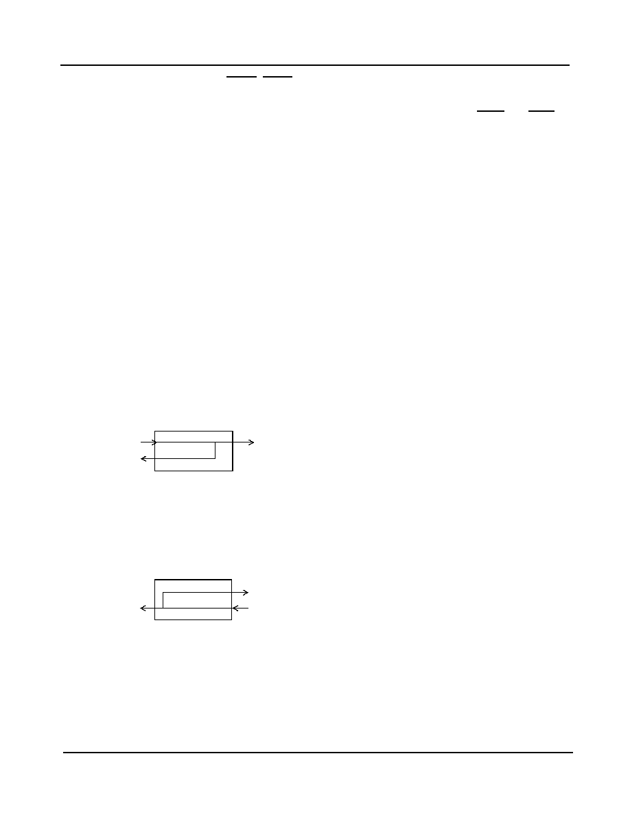
MT9072
Data Sheet
82
Zarlink Semiconductor Inc.
10.1.7 Multiframe Boundary (RxMF, TxMF Pins)
Dedicated multiframe boundary pins are included which provide the user the option of setting the multiframe
boundaries and identifying the multiframe boundaries with an external device. Refer to the RxMF and TxMF pin
descriptions for more details.
11.0 ST-BUS Analyzer
The ST-BUS Analyzer is a powerful system diagnostic and debugging tool. The ST-BUS Analyzer allows for the
capture of any ST-BUS data stream or channel to a 32 byte memory. The ST-BUS Analyzer can capture a single
frame of data or 32 samples of a specified channel from DSTi, DSTo, CSTi or CSTo from any one of the 8 framers.
The analysis can be performed continuously or on a single shot basis where 32 bytes are captured and then the
analysis is suspended. An optional interrupt can be generated when a single shot analysis is complete. The
operation of the ST-BUS analyzer is controlled by Global Control Register 1 (901).
12.0 Loopbacks
12.1 T1 Loopbacks
In order to meet PRI Layer 1 requirements and to assist in circuit fault sectionalization, the MT9072 has 7 loopback
functions.
The control bits for digital, remote, ST-BUS and payload loopbacks are located at address Y05. The remote and
local timeslot loopbacks are controlled through control bits of the Timeslot Control register located at addresses
Y90-YA7.
a) Digital loopback (DG Loop) - DSTi to DSTo at the PCM24 side. Bit DLBK = 0 normal; DLBK = 1 activate.
b) Payload loopback (PL Loop) - Payload loopback (DSTo to DSTi). Bit PLBK = 0 normal; PLBK = 1 activate. The
payload loopback is effectively a physical connection of DSTo to DSTi within the framer.
Note: Set RxDO (YF1 bit 9 to 1) to obtain correct data at the Tx.
c) Local and Remote Timeslot Loopback. Remote timeslot loopback control bit RTSL = 0 normal; RTSL = 1 activate
(Register Y90-YA7) will loop around transmit ST-BUS timeslots to the DSTo stream. Local timeslot loopback bits
LTSL = 0 normal; LTSL = 1 activate(Register Y90-YA7), will loop around receive PCM24 timeslots towards the
remote PCM24 end.
MT9072
Tx
DSTi
DSTo
System
PCM24
MT9072
Tx
DSTi
DSTo
System
PCM24
Rx
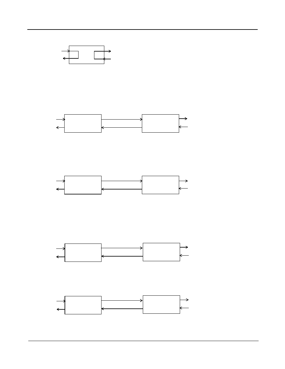
MT9072
Data Sheet
83
Zarlink Semiconductor Inc.
d) Framer Remote loopback - Internally connects RPOS and RNEG of one framer to TPOS and TNEG respectively
of one of the other integrated framers.
Bit RLBK01, RLBK23, RLBK45, RLBK67 = 0 normal; = 1 activate.
8 Mbit/s mode:
Bit RLBK8 = 0 normal; = 1 activate.
e) Framer ST-BUS loopback(Register 904) - Internally connects DSTi of one framer to DSTo of one of the other
integrated framers.
Bit SLBK01, SLBK23, SLBK45, SLBK67 = 0 normal; = 1 activate.
8 Mbit/s mode:
Bit SLBK8 = 0 normal; = 1 activate.
MT9072
Tx
DSTi
DSTo
System
PCM24
Rx
MT9072 Framer 0,2,4,6
Tx
DSTo
System
PCM24
Rx
DSTi
MT9072 Framer 1,3,5,7
DSTo
System
DSTi
Tx
Rx
MT9072 Framer 0-3
Tx
DSTo[0]
System
PCM24
Rx
DSTi[0]
MT9072 Framer 4-7
DSTo[4]
System
DSTi[4]
Tx
Rx
MT9072 Framer 0,2,4,6
Tx
DSTo
System
PCM24
Rx
DSTi
MT9072 Framer 1,3,5,7
DSTo
DSTi
Rx
Tx
PCM24
MT9072 Framer 0-3
Tx
DSTo[4]
System
PCM24
Rx
DSTi[0]
MT9072 Framer 4-7
DSTo[0]
DSTi[4]
Rx
Tx
PCM24

MT9072
Data Sheet
84
Zarlink Semiconductor Inc.
12.2 T1 In Band Loopback Codes
T1.403 defines SF mode line loopback activate and deactivate codes. These codes are either a framed or
unframed repeating bit sequence of 00001 for activation or 001 for deactivation. The standard goes on to say that
these codes will persist for five seconds or more before the loopback action is taken. The MT9072 will detect both
framed and unframed line activate and de-activate codes even in the presence of a BER of 3 x 10
-3
. Line Loopback
Disable Detect - LLDD - in the Alarm Status Word (Y10) will be asserted when a repeating 001 pattern (either
framed or unframed) has persisted for 48 milliseconds. Line Loopback Enable Detect LLED in the Alarm Status
Word will be asserted when a repeating 00001 pattern (either framed or unframed) has persisted for 48
milliseconds.
Other loopup and loopdown codes can be selected by writing to Transmit Loop Activate and Loop Deactivate Code
registers(Y0D and Y0E).
The selection of the expected received loopup and loopdown code is done by writing to registers Receive Loopup
Code and Receive Loop Deactivate Code Match registers(Y0F and YF0).
Interrupt status bits LLEDI and LLDDI will be set upon detection of inband loopup or loopdown codes respectively.
Maskable interrupts can be generated by disabling the mask bits in Receive line status and Timer mask (Y45 bit 5).
Register
Address
Register
Description
Y05
Loopback Control
This register contains the loopbacks within the framer.
Y90-YAF
Per Channel Control
RTSL and LTSL are per channel loopbacks.
904
Framer Loopback Global Register This register contains framer to framer loopbacks.
Table 38 - Registers Related to Loopbacks (T1)
Register
Address
Register
Description
Y02
Transmit Alarm Control
If the SO bit is set, there will be framed loop codes, otherwise they will be
unframed.
Y05
Loopback Control
Setting TLU or TLD will cause the transmitter to start sending the
appropriate loopup and loopdown code.
Y0D
Transmit Loop Activate
Code
This register contains the loop activate code which will be sent on the Tx
PCM stream when TLU is set. It also contains 2 bits for code length.
Y0E
Transmit Loop Deactivate
Code
This register contains the loop deactivate code which will be sent on the
Tx PCM stream when TLD is set. It also contains 2 bits for code length.
Y0F
Receive Loop Activate
Code Match
This register contains the loop activate code which will cause an interrupt
if received on the RX PCM stream. It also contains 2 bits for code length.
YF0
Receive Loop Deactivate
Code Match
This register contains the loop deactivate code which we are looking for
on the RX PCM stream. It also contains 2 bits for code length.
Y10
Synchronization and
Alarm Status
LLED and LLDD will be high when their respective loop codes are
detected in the match registers.
Table 39 - Registers Related to In Band Loopbacks (T1)

MT9072
Data Sheet
85
Zarlink Semiconductor Inc.
12.3 E1 Loopbacks
In order to meet PRI Layer 1 requirements and to assist in circuit fault sectionalization, the MT9072 has 7 loopback
functions.
Table 40 specifies the registers related to controlling the different loopbacks.
a) Digital loopback (DG Loop) - DSTi to DSTo at the PCM30 side. Bit DLBK = 0 normal; DLBK = 1 activate.
The control bits for digital, remote, ST-BUS and payload loopbacks are located at address Y05. The remote and
local timeslot loopbacks are controlled through control bits of the Timeslot Control register located at addresses
Y90-YAF.
b) Payload loopback (PL Loop) - Payload loopback (DSTo to DSTi). Bit PLBK = 0 normal; PLBK = 1 activate. The
payload loopback is effectively a physical connection of DSTo to DSTi within the MT9072.
Y35
Receive Line and Timer
Interrupt Status
LLEI and LLDI are the interrupts for LLED and LLDD.
Y45
Receive Line and Timer
Interrupt Mask
LLEIM and LLDIM are the masks for LLEI and LLDI.
Register
Address
Register
Description
Y01
Test, Error and Loopback
Control Register
The bits DLBK,RLBK, SLBK and PLBK can be used for digital
loopback, remote loopback, ST-BUS and loopback.
Y02
Interrupt and IO control register RxDO and RxCO have to one for certain loopbacks to work.
Y90 to YAF
Timeslot Control Register
Local and Remote Timeslot Control Register allows for Timeslot
Loopbacks (RTSLand TTSL).
904
Framer Loopback Global
Register
Framer to Framer ST-BUS and Remote Loopbacks.
Table 40 - Register Related to Setting Up Loopbacks (E1)
Register
Address
Register
Description
Table 39 - Registers Related to In Band Loopbacks (T1)
MT9072
Tx
DSTi
DSTo
System
PCM30
MT9072
Tx
DSTi
DSTo
System
PCM30
Rx
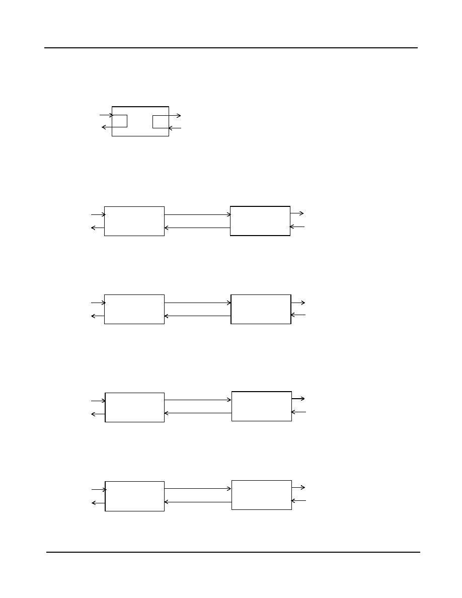
MT9072
Data Sheet
86
Zarlink Semiconductor Inc.
c) Local and Remote Timeslot Loopback. Remote timeslot loopback control bit RTSL = 0 normal; RTSL = 1
activate, will loop around transmit ST-BUS timeslots to the DSTo stream. Local timeslot loopback bits LTSL = 0
normal; LTSL = 1 activate, will loop around receive PCM30 timeslots towards the remote PCM30 end.
d) Framer Remote loopback - Internally connects RPOS and RNEG of one framer to TPOS and TNEG respectively
of one of the other integrated framers.
Bit RLBK01, RLBK23, RLBK45, RLBK67 = 0 normal; = 1 activate.
8 Mbit/s mode:
Bit RLBK8 = 0 normal; = 1 activate.
e) Framer ST-BUS loopback - Internally connects DSTi of one framer to DSTo of one of the other integrated
framers.
Bit SLBK01, SLBK23, SLBK45, SLBK67 = 0 normal; = 1 activate.
8 Mbit/s mode:
Bit SLBK8 = 0 normal; = 1 activate.
MT9072
Tx
DSTi
DSTo
System
PCM30
Rx
MT9072 Framer 0,2,4,6
Tx
DSTo
System
PCM30
Rx
DSTi
MT9072 Framer 1,3,5,7
DSTo
System
DSTi
Tx
Rx
MT9072 Framer 0-3
Tx
DSTo[0]
System
PCM30
Rx
DSTi[0]
MT9072 Framer 4-7
DSTo[4]
System
DSTi[4]
Tx
Rx
MT9072 Framer 0,2,4,6
Tx
DSTo
System
PCM30
Rx
DSTi
MT9072 Framer 1,3,5,7
DSTo
DSTi
Rx
Tx
PCM30
MT9072 Framer 0-3
Tx
DSTo[4]
System
PCM30
Rx
DSTi[0]
MT9072 Framer 4-7
DSTo[0]
DSTi[4]
Rx
Tx
PCM30

MT9072
Data Sheet
87
Zarlink Semiconductor Inc.
13.0 Performance Monitoring
13.1 T1 Error Counters
The MT9072 has nine error counters for each framer, which can be used for maintenance testing and ongoing
measurement of the quality of a DS1 link and to assist the designer in meeting specifications such as TR62411 and
T1.403. All counters can be preset or cleared by writing to the appropriate counter registers.
Associated with each counter is a maskable event occurrence interrupt and a maskable counter overflow interrupt.
Overflow interrupts are useful when cumulative error counts are being recorded. For example, every time the
framing bit error counter overflow interrupt (FEO) occurs, 65536 frame errors have been received since the last
FEO interrupt. Also if a counter overflows, the overflow indicators are latched in the Overflow reporting latch
register(Y24).
All counters are cleared by a counter clear bit -CNTCLR - low to high transition (bit 2 of the IO Control Word, YF1).
An alternative approach to event reporting is to mask error events and to enable the 1 second sample bit (SAMPLE
- bit 1 of the Interrupt and IO Control Word). When this bit is set the latched version of the counters(Y28 to Y2C) for
change of frame alignment, loss of frame alignment, bpv errors, crc errors, errored framing bits, and multiframes out
of sync are updated on one second intervals coincident with the maskable one second interrupt timer.
.
Counter
Interrupt Status Bits
1 Second Latch
Description
Bits
Address Indication
Overflow
Description
Bit
Address
PRBS Error Counter
and CRC Multiframe
counter for PRBS
PS7-0,
PSM7-0
Y15
PRBSI
PRBSOI
PRBSMFOI
NA
NA
NA
Multiframe Out of
Frame Counter
MFOOF
7-0
Y16
MFOOFI
MFOOFOI Multiframe Out of
Frame Count Latch
MFOO
FL15-0
Y2C
Framing Bit Error
Counter
FC15-0
Y17
FBEI
FEOI
Framing Bit Error
Counter Latch
FCL15-
0
Y28
BPV Counter
BPV15-0
Y18
BPVI
BPVOI
Bipolar Violation
Count Latch
BPVL
15-0
Y29
CRC-6 Error counter
CC15-0
Y19
CRCI
CRCOI
CRC-6 Error Count
Latch
CRCL
15-0
Y2A
Out of frame counter,
change of frame
alignment counter
OOF7-0,
COFA7-0
Y1A
OOFOI
COFAI
OOFOI
COFOIL
Out of Frame, Change
of Frame Alignment
Count Latch
OOFL
7-0
COFAL
7-0
Y2B
Excessive Zero
counter
EXZ7-0,
Y1B
EXZI
EXZOL
NA
NA
NA
Table 41 - Error Counters Summary (T1)

MT9072
Data Sheet
88
Zarlink Semiconductor Inc.
13.2 E1 Error Counters
The MT9072 has eight error counters, which can be used for maintenance testing, and ongoing measurement of
the quality of a PCM30 link and to assist the designer in meeting specifications such as ITU-T I.431 and G.821. All
counters can be preset or cleared by writing to the appropriate locations. In addition, four error count latches are
provided which latch the counter data coincident with the one second status bit. Counters can automatically be
cleared (ACCLR register address Y03) after their data is latched. Associated with each counter is a maskable event
indication interrupt and a maskable counter overflow interrupt. Overflow interrupts are useful when cumulative error
counts are being recorded. For example, every time the frame error counter overflow (FEO) interrupt occurs, 256
frame errors have been received since the last FEO interrupt. The interrupt status register bits are cleared when
read. All non-latched error counters are cleared and by programming the counter clear bit (CNCLR register address
Y03) low to high. See Table 43 for counter events and relationship between the counters.
Register
Address
Register
Description
Y03
DL,CCS,CAS and other
Control Register
The CNCLR bit can be used to clear the non-latched counters.
the ACCLR can be used to automatically clear 1 sec counter.
Y15
PRBS Error Counter and
CRC-4 Multiframe Counter
PRBS counts bit errors and the CRC counter interval for each
received multiframe.
Y16
Loss of basic frame counter
Counter that is incremented once per 125 usec whenever bsync
is 1.
Y17
E-bit error counter
This counter counts the ebit errors.
Y18
Bipolar violation counter. This
counter counts the bipolar
violation outside the HDB3
coding.
This counter counts the bipolar violation outside the HDB3
coded zeros.
Y19
CRC-4 error counter
This counter is incremented for calculated crc-4 errors (CRCS1
and CRCS2).
Y1A
FAS bit error counter and FAS
error counter
This counter counts the FAS bit error and FAS errors.
Y28
E bit error counter latch
This counter is the one second latched version of Y17.
Y29
BPV error counter latch
This counter is a one second latched version of Y18.
Y2A
CRC-4 error counter latch
This counter is a one second latched version of Y19.
Y2B
FAS error counter latch
This counter is a one second latched version of Y1A.
Y36
CAS,National, CRC-4 local
and timer interrupt status
register
Oneseci is the one second interrupt status. This interrupt can be
used for performance monitoring.
Y46
CAS,National, CRC-4 local
and timer interrupt mask
register
Onesecm is the one second interrupt status. This interrupt can
be used for performance monitoring.
Table 42 - Registers Required for Observing and Clearing Error Counters (E1)

MT9072
Data Sheet
89
Zarlink Semiconductor Inc.
14.0 Maintenance and Alarms
14.1 T1 Maintenance and Alarms
14.1.1 T1 Error Insertion
Six types of error conditions can be inserted into the transmit DS1 data stream through control bits, which are
located in address Y03 -Transmit Error Control Word. These error events include bipolar violation errors (BPVE),
CRC-6 errors (CRCE), Ft errors (FTE), Fs errors (FSE), payload errors (PERR) and a loss of signal condition
(LOSE). If LOSE is one the selected framer transmits an all zeros signal (no pulses) and zero code suppression is
overridden. If LOSE bit is zero, data is transmitted normally.
14.1.2 T1 Per Timeslot Control
There are 24 per timeslot control registers occupying a total of 24 unique addresses (Y90-YA7). Each register
controls a transmit timeslot and the equivalent channel data on DSTo. For example, register address Y90 of the first
per timeslot control register contains program control for transmit timeslot 0 and DSTo channel 0.
14.1.3 T1 Per Timeslot Looping
Any channel or combination of channels may be looped from transmit (sourced from DSTi) to receive (output on
DSTo) ST-BUS channels. When bit 4 (LTSL) in the Per Timeslot Control Word(Y90-YA7) is set the data from the
equivalent transmit channel is looped back onto the equivalent receive timeslot.
Any channel or combination of channels may be looped from receive (sourced from the line data) to transmit
(output onto the line) channels. When bit 5 (RTSL) in the Per Timeslot Control Word is set the data from the
equivalent receive timeslot is looped back onto the equivalent transmit timeslot.
Counter
Source Interrupt Status Bits
1 Second Latch
Description
Bits
Address
Bit
Indication Overflow Description
Bit
Address
PRBS Error Counter PEC7-0
Y15
PEI
PEO
NA
NA
NA
PRBS CRC-4 MF
Counter
PCC7-0
Y15
CALN
NA
PCO
NA
NA
NA
Loss of Sync
Counter
SLC7-0
Y16
BSYNC
BSYNC
SLO
NA
NA
NA
E-bit Error Counter
EEC15-0
Y17
REB1
REB2
EEI
EEO
E-bit Error
Count Latch
EEL15-0
Y28
BPV Error Counter
VEC15-0
Y18
VEI
VEO
BPV Error
Count Latch
VEL15-0
Y29
CRC-4 Error
Counter
CEC15-0
Y19
CRCS1
CRCS2
CEI
CEO
CRC-4 Error
Count Latch
CEL15-0
Y2A
FAS Bit Error
Counter
BEC7-0
Y1A
BEI
BEO
FAS Bit Error
Count Latch
BEL7-0
Y2B
FAS Error Counter
FEC7-0
Y1A
FEI
FEO
FAS Error
Count Latch
FEL7-0
Y2B
Table 43 - Error Counter and Event Dependency (E1)

MT9072
Data Sheet
90
Zarlink Semiconductor Inc.
14.1.4 T1 Pseudo-Random Bit Sequence (PRBS) Testing
The MT9072 includes both a pseudo random bit sequence (PRBS) generator of type (2
15
-1), and a reverse PRBS
generator (decoder), which operates on a bit sequence, and determines if it matches the transmitted PRBS type
(2
15
-1). Bits which don't match are counted by an internal error counter. This provides for powerful system
debugging and testing without additional external hardware.
If control bit ADSEQ (register address Y01) is zero, any transmit (internal DSTi) timeslot or combination of transmit
timeslots may be connected to the PRBS generator. Timeslot n is selected by setting the TTSTn bit in the Timeslot
n Control Register (address Y90-YA7), where n is 0 to 23. Any data sent on DSTi is overwritten on the selected
timeslots before being output to TPOS/TNEG.
Similarly, if control bit ADSEQ is zero, any receive timeslot or combination of receive timeslots may be connected to
the PRBS decoder. Timeslot n is selected by setting the RRSTn bit in the Timeslot n Control Register (register
address Y90-YA7), where n is 0 to 23.
PRBS data is distributed to the transmit channels sequentially one byte at a time. Consequently, the data received
must be in the same order that it was sent, in order for the PRBS decoder to correctly operate on the data.
If one channel is tested at a time, then the PRBS transmit timeslot does not have to match the PRBS receive
timeslot. However, if more than one channel is tested, then the number of transmit timeslots must match the
number of receive timeslots, and the order of the transmit timeslots must match the order of the receive timeslots.
This will ensure that the sequential data bytes received by the PRBS decoder are in the correct order.
Consequently, particular care must be taken when using an external loopback where the channel order may be
reversed, or where the data has passed through a digital switch which doesn't buffer all channels to the same
degree.
The PRBS decoder must have sufficient data pass through it before it begins to operate correctly, therefore, the
errors generated by the decoder immediately following start-up should be ignored.
If the PRBS testing is performed in an external loop around using Timeslot Control, then both Timeslot Control bits
TTSTn and RRSTn should also be set.
Register
Address
Register
Description
Y01
Line Interface and Coding
ADSEQ bit chooses between Milliwatt test sequence and
transmitted PRBS test sequence.
Y90-YA7
Per Channel Control
If TTST is set for any channel, the test sequence will be
transmitted on that DS1 timeslot. If RRST is set for any channel,
the test sequence will be expected on the receivePCM24 slot.
Y15
PRBS Error Counter and CRC
Multiframe Counter for PRBS
The PRBS Error Counter contains error count on the received
PRBS sequence.
Y34
Receive Sync Interrupt Status
PRBSOI will indicate an overflow on the PRBS Error Counter.
Y44
Receive Sync Interrupt Mask
PRBSOIM is the mask for PRBSOI.
Table 44 - Registers Related to PRBS Testing (T1)

MT9072
Data Sheet
91
Zarlink Semiconductor Inc.
14.1.5 T1 Mu-law Milliwatt
If the control bit ADSEQ is one (register address Y01), the Mu-law digital milliwatt sequence (Table 45) defined by
G.711, is available to be transmit on any combination of selected channels. The channels are selected by setting
the TTSTn control bit (register address Y90-YA7). The same sequence is available to replace received data on any
combination of DSTo channels. This is accomplished by setting the RRSTn control bit (register address Y90-YA7)
for the corresponding channel. Note that Bit 1 is the sign bit and is sent first.
14.1.6 T1 Alarms
The alarms shown in Table 46 are detected by the receiver. The status register bits provide real time status of the
alarm, while the interrupt status registers bits provide latched status indications which are cleared when read. Each
interrupt status register may also generate a maskable interrupt. The possible transmitted alarms are also shown in
the table. See the register bit descriptions for details.
PCM 24 Payload Data
Hex
Bit 1
Bit 2
Bit 3
Bit 4
Bit 5
Bit 6
Bit 7
Bit 8
1E
0
0
0
1
1
1
1
0
0B
0
0
0
0
1
0
1
1
0B
0
0
0
0
1
0
1
1
1E
0
0
0
1
1
1
1
0
1E
1
0
0
1
1
1
1
0
8B
1
0
0
0
1
0
1
1
8B
1
0
0
0
1
0
1
1
9E
1
0
0
1
1
1
1
0
Table 45 - Mu Law Digital Milliwatt Pattern (T1)
Control/Status Register
Interrupt Status
Register
Description
Bit
Address
Bit
Address
D4 Yellow Alarm. This bit is set if bit position 2 of virtually every
DS0 channel is a zero for a period of 600 milliseconds. The alarm is
tolerant of errors by permitting up to 16 ones in a 48 millisecond
integration period. The alarm clears in 200 milliseconds after being
removed from the line.
D4YALM
Y10
D4YALMI
Y35
D4 Yellow Alarm - 48 millisecond sample. This bit is set if bit
position 2 of virtually every DS0 channel is a zero for a period of 48
milliseconds. The alarm is tolerant of errors by permitting up to 16
ones in the integration period. This bit is updated every 48
milliseconds.
D4Y48
Y10
D4Y48I
Y35
Table 46 - Alarm Control and Status Bits (T1)

MT9072
Data Sheet
92
Zarlink Semiconductor Inc.
14.1.7 T1 Per Timeslot Trunk Conditioning
The per channel conditioning capabilities of MT9072 are explained in this section. For the receiver the T1 data can
be replaced by the conditioning data (Y09) via the bit MPDR in the per channel control registers(Y90 to YA7).
This data will be output to the corresponding DSTo channel. The received data can be inverted on a per channel
basis by setting the RPCI bit (register Y90 to YA7). The transmit data can be inverted on a per channel basis with a
write to the control bit TPCI (registers Y90 to YA7). The transmit data can also be frozen on a per channel basis; in
this case the data from the DSTI is not used to update the Transmit Memory and the data written in Y0A is used as
the source (MPDT in registers Y90 to YA7).
Secondary D4 Yellow Alarm. This bit is set if 2 consecutive'1's are
received in the S-bit position of the 12th frame of the D4
superframe.
SECYEL
Y10
SECYELI
Y35
AIS Alarm. This bit is set if fewer than 5 zeros are received in a 3
millisecond window.
AIS
Y10
AISI
Y35
ESFYEL.This bit is set if the ESF yellow alarm 0000000011111111
is receive in eight or more codewords out of ten in Bit Oriented
Message of FDL.
ESFYEL
Y10
ESFYELI
Y35
T1DM Received Yellow Alarm. If "Y" bit of the T1DM
Synchronization Word is received
T1DRY
Y10
T1DMYI
Y35
Transmit ESF Yellow Alarm. Setting this bit (while in ESF mode)
causes a repeating pattern of eight 1's followed by eight 0's to be
insert onto the transmit FDL.
TESFYEL
Y02
NA
NA
Transmit Secondary D4 Yellow Alarm. Setting this bit (in D4
mode) causes the S-bit of transmit frame 12 to be set.
TSECY
Y02
NA
NA
Transmit All Ones. When low, this control bit forces a framed or
unframed (depending on the state of Transmit Alarm Control bit 0)
all ones to be transmit at TTIP and TRING
TAIS
Y02
NA
NA
S-bit Override. If set, this bit forces the S-bits to be inserted as an
overlay on any of the following alarm conditions: i) transmit all ones,
ii) loop up code insertion, iii) loop down code insertion.
SO
Y02
NA
NA
TT1DMY. If reset to low a yellow alarm is sent in the 24th channel if
the T1DM option is set.
TT1DMY
Y02
NA
NA
Control/Status Register
Interrupt Status
Register
Description
Bit
Address
Bit
Address
Table 46 - Alarm Control and Status Bits (T1)

MT9072
Data Sheet
93
Zarlink Semiconductor Inc.
14.2 E1 Maintenance and Alarms
Extensive maintenance and alarm generation and detection functions are provided on the MT9072. The following
table groups the registers for control and monitor of these functions.
14.2.1 E1 Error Insertion
Six types of error conditions can be inserted into the transmit PCM30 data stream through register control bits
located at address Y01. These error events include the bipolar violation errors (BVE), CRC-4 errors (CRCE), FAS
errors (FASE), NFAS errors (NFSE), payload (PERR) and a loss of signal error (LOSE). The LOSE function
overrides the HDB3 encoding function (no BPV are added). Also included are E1 and E2 error bit insertion on
frames 13 and 15. See the bit descriptions (control register address Y01) for additional details.
14.2.2 E1 Per Timeslot Control
There are 32 per timeslot control registers occupying a total of 32 unique addresses (Y90-YAF). Each register
controls a matching timeslot on the 32 transmit channels (onto the line) and the equivalent channel data on the
receive (DSTo) data. For example, register address Y91 of the first per timeslot control register contains program
control for transmit timeslot 1 and DSTo channel 1.
14.2.3 E1 Per Timeslot Looping
Any channel or combination of channels may be looped from transmit (sourced from DSTi) to receive (output on
DSTo) ST-BUS channels. When bit 4 (LTSL) in the Per Timeslot Control Word is set the data from the equivalent
transmit timeslot is looped back onto the equivalent receive channel.
Any channel or combination of channels may be looped from receive (sourced from the line data) to transmit
(output onto the line) channels. When bit 5 (RTSL) in the Per Timeslot Control Word is set the data from the
equivalent receive timeslot is looped back onto the equivalent transmit channel.
Register
Address
Register
Description
Y00
Alarm and Framing Control Register The TAIS and E bit errors and RAI can be set by this register.
Y01
Test Error and Loopback Control
Register
BPVE, CRCE,FASE, NFSE and E bit errors can be inserted.
Y05
CAS Control and Data Register
The Y bit can be used to send Remote Multiframe Alarm signal.
Y10
Synchronization and CRC-4
Remote Status
The bits of this register provide good receiver error status.
Y11
CRC-4 Timer and CRC-4 Local
Status
The CRC-4 errors are registered in Y11.
Y12
Alarms and MAS Status
This register provides AIS, RAI, LOSS status bits.
Y24
Sync, CRC-4 remote alarm, MAS
Latched Status Register
Latched version of receive CRC errors and synchronization loss
are available.
Y34
Sync, CRC-4 Remote Alarm, MAS
Interrupt status register
This register provides bits for interrupt generation for Y24 CRC
errors and synchronization loss functions.
Y44
Sync, CRC-4 Remote Alarm, MAS
Interrupt register mask
This register provides bits for interrupt mask register for Y34.
Table 47 - Registers Related to Maintenance and Alarms (E1)

MT9072
Data Sheet
94
Zarlink Semiconductor Inc.
14.2.4 E1 Pseudo-Random Bit Sequence (PRBS) Testing
The MT9072 includes both a pseudo random bit sequence (PRBS) generator of type (2
15
-1), and a reverse PRBS
generator (decoder), which operates on a bit sequence, and determines if it matches the transmitted PRBS type
(2
15
-1). Bits which don't match are counted by an internal error counter. This provides for powerful system
debugging and testing without additional external hardware.
If control bit ADSEQ (register address Y01) is zero, any transmit (internal DSTi) timeslot or combination of transmit
timeslots may be connected to the PRBS generator. Timeslot n is selected by setting the TTSTn bit in the Timeslot
n Control Register (address Y90-YAF), where n is 0 to 31. Any data sent on DSTi is overwritten on the selected
timeslots.
Similarly, if control bit ADSEQ is zero, any DSTo receive timeslot or combination of receive timeslots may be
connected to the PRBS decoder. Timeslot n is selected by setting the RRSTn bit in the Timeslot n Control Register
(register address Y90-YAF), where n is 0 to 31. Data on DSTo is not affected.
PRBS data is distributed to the transmit channels sequentially one byte at a time. Consequently, the data received
must be in the same order that it was sent, in order for the PRBS decoder to correctly operate on the data.
The number of transmit timeslots must match the number of receive timeslots, and the order of the transmit
timeslots must match the order of the receive timeslots. This will ensure that the sequential data bytes received by
the PRBS decoder are in the correct order. Consequently, particular care must be taken when using an external
loopback where the channel order may be reversed, or where the data has passed through a digital switch which
doesn't buffer all channels to the same degree.
The PRBS decoder must have sufficient data pass through it before it begins to operate correctly, therefore, the
errors generated by the decoder immediately following start-up should be ignored.
If the PRBS testing is performed in an external loop around using Timeslot Control, then both Timeslot Control bits
TTSTn and RRSTn should also be set.
14.2.5 E1 A-law Milliwatt
If the control bit ADSEQ is one (register address Y01), the A-law digital milliwatt sequence (Table 48), defined by
G.711, is available to be transmit on any combination of selected channels. The channels are selected by setting
the TTSTn control bit (register address Y90-YAF). The same sequence is available to replace received data on any
combination of DSTo channels. This is accomplished by setting the RRSTn control bit (register address Y90-YAF)
for the corresponding channel. Note that bit 1 is the sign bit and is sent first.
PCM30 Payload Data
Hex
Bit 1
Bit 2
Bit 3
Bit 4
Bit 5
Bit 6
Bit 7
Bit 8
34
0
0
1
1
0
1
0
0
21
0
0
1
0
0
0
0
1
21
0
0
1
0
0
0
0
1
34
0
0
1
1
0
1
0
0
B4
1
0
1
1
0
1
0
0
A1
1
0
1
0
0
0
0
1
A1
1
0
1
0
0
0
0
1
B4
1
0
1
1
0
1
0
0
Table 48 - A-Law Digital Milliwatt Pattern (E1)

MT9072
Data Sheet
95
Zarlink Semiconductor Inc.
14.2.6 E1 Alarms
The alarms shown in Table 49 are detected by the receiver. The status register bits provide real time status of the
alarm, while the latched status registers provide a latched status indication, and the interrupt status registers
provide a latched status indication (if unmasked) which generate a maskable interrupt and which are cleared when
read. The persistent status registers provide latched status indication which is only cleared when read while the real
time status bit is not set. See the register bit descriptions for additional details.
14.2.7 E1 Automatic Alarms
The transmission of RAI and signaling multiframe alarms can be made to function automatically from control bits
ARAI and AUTY (register address Y00). When ARAI = 0 and basic frame synchronization is lost (BSYNC = 1
address Y10), the MT9072 will automatically transmit the RAI alarm signal to the far end of the link. The
transmission of this alarm signal will cease when basic frame alignment is acquired.
When AUTY = 0 and signaling multiframe alignment is not acquired (MSYNC = 1 address Y10), the MT9072 will
automatically transmit the multiframe alarm (Y-bit) signal to the far end of the link. This transmission will cease
when signaling multiframe alignment is acquired.
Description
Status
Register
Latched Status
Register
Interrupt Status
Register
Persistent Status
Register
Bit
Add.
Bit
Add.
Bit
Add.
Bit
Add.
Remote Alarm Indication
RAI
Y12
RAIL
Y24
RAII
Y34
RAIP
Y27
Alarm Indication Signal
AIS
Y12
AISL
Y24
AISI
Y34
AISP
Y27
Alarm Indication Signal 100ms
KLVE
Y12
Channel 16 Alarm Indication
Signal
AIS16
Y12
AIS16L
Y24
AIS16I
Y34
Auxiliary Pattern
AUXP
Y12
AUXPL
Y24
AUXPI
Y34
Loss of Signal
LOSS
Y12
LOSSL
Y24
LOSSI
Y34
LOSSP
Y27
Remote signaling Multiframe
Alarm
Y
Y12
YL
Y24
YI
Y34
T1 Timer
T1
Y11
T1L
Y26
T1I
Y36
T2 Timer
T2
Y11
T2L
Y26
T2I
Y36
Table 49 - Alarms and Timers Status Registers (E1)
MT9072
Data Sheet
96
Zarlink Semiconductor Inc.
15.0 Interrupts
The MT9072 has an extensive suite of interrupts consisting of 2 maskable interrupt vectors and 32 maskable
interrupt status registers as shown in Figure 9 and an ST-BUS Analyzer Interrupt. The set bits in the 2 interrupt
vectors identify which of the 32 interrupt status registers is responsible for the interrupt. Reading the corresponding
interrupt status registers identifies the exact source of the interrupt. Any set bit in the interrupt vectors causes the
IRQ pin to toggle low (providing the SPND bit is not set).
Figure 9 - Interrupt Status Registers
F
R
A
M
E
R
1
Elastic
Interrupt
Status
Register
036
Rx Sync
Interrupt
Status
Register
034
Rx Line
Status
Register
035
Elastic
Store
Mask
Status
046
Rx Sync
Mask
Status
Register
044
RX Line
Mask
Status
Register
045
Framer 0 Master LatchStatus
Registers 023 - 026
FRAMER 0
INTA
SPND
F
R
A
M
E
R
2
F
R
A
M
E
R
3
F
R
A
M
E
R
5
F
R
A
M
E
R
6
F
R
A
M
E
R
7
F
R
A
M
E
R
4
4
Interrupt Vector 1
Status Register Address 910
Interrupt Vector 1
Mask Register Address 902
4
4
4
4
4
4
4
4
4
4
4
IRQ
Pin
Interrupt Vector 1
Interrupt Vector 2
Status Register Address 911
Interrupt Vector 2
Mask Register Address 903
Interrupt Vector 2
IRQ 1
IRQ 2
HDLC
Status
Register
033
HDLC
Mask
Status
Register
043
ST-BUS
Analyser
Interrupt

MT9072
Data Sheet
97
Zarlink Semiconductor Inc.
15.1 Interrupt Status Register Overview
All 33 interrupt status registers are maskable with 33 corresponding interrupt mask registers. All interrupt status
registers and all interrupt mask registers are 16 bits, although all 16 bits are not always used. Unused status bits
may be either one or zero if read.
When an unmasked interrupt occurs, one or more bits of the 33 interrupt status registers will go high causing one or
more bits of the unmasked interrupt vector to go high. A high bit in the interrupt vector causes the output IRQ pin to
go low (if enabled by SPND, INTA control bits). After an interrupt status register is read, it is automatically cleared.
After all interrupt status registers are cleared, the interrupt vector is cleared causing the IRQ pin to return to a high
impedance state.
If a new unmasked interrupt occurs while the interrupt status registers from a previous interrupt are being read, the
affected interrupt status registers will be updated, the interrupt vector will be updated, and the IRQ pin will remain
low until all interrupt status registers are cleared.
If the interrupt status registers are unmasked, and the interrupt vector is masked, the interrupt status registers will
function normally, but they will not cause the IRQ pin to toggle low. Only set bits in the Interrupt Vector will cause the
IRQ pin to toggle low. This is similar to the SPND control bit function, but instead of masking all selected framer
interrupts, the interrupt vector mask can mask individual registers within the selected framers.
15.1.1 Interrupt Related Control Bits and Pins
SPND - All interrupts for a particular framer may be suspended without changing the interrupt mask words, by
setting the
SPND
control bit (register address YF1) to zero. All unmasked interrupt status registers will continue to
be updated (and will be cleared when read), but the selected framers interrupt vector bits will remain at zero.
Therefore that framer cannot toggle the IRQ pin. If all eight framer's SPND bit are zero, then all interrupt vector bits
will remain low, therefore none of the framers can toggle the IRQ pin.
In some applications, a logic low at the IRQ pin lasting the full duration of the interrupt service routine may be
undesirable. In these cases, immediately following the interrupt, set the control bit SPND (register address YF1) low
until the interrupt service routine is finished
INTA - All interrupt and latched status registers for a particular framer may be cleared (without reading the interrupt
status registers) by setting the INTA control bit (register address YF1) to zero. Interrupt status and latched registers
for a particular framer will be cleared (and not updated) as long as INTA is low. Consequently, the selected framer's
interrupt vector bits will remain at zero, therefore that framer cannot toggle the IRQ pin.
TAIS - During initial power up, all (8 framers) interrupt status registers are cleared without changing the interrupt
mask words, when the TAIS control pin is held low. Consequently, the interrupt vector will remain clear and the IRQ
pin will remain in a high impedance state. This allows for system initialization without spurious interrupts. Interrupt
status registers will not be updated, and the IRQ pin will be forced to a high impedance state as long as TAIS is low.
RESET or RST - After a MT9072 reset (RESET pin for all eight framers or RST control bit (register address YF1)
for a selected framer), all interrupt status register bits are unmasked, but the SPND and INTA control bits are set to
zero.
15.2 Interrupt Servicing Methods
There are two common methods for identifying the source of an interrupt. The Polling Method is the simplest but
uses the most processor time. The Vector Method requires a two step process, but uses the least amount of
processor time.

MT9072
Data Sheet
98
Zarlink Semiconductor Inc.
15.2.1 Polling Method
1. The IRQ pin goes low.
2. Read all 33 interrupt vector status registers. The bits which are set in these registers identify the source of the
interrupt. As each register is read, it is cleared (all bits set to 0). When all registers are clear, the interrupt is cleared
(the IRQ pin returns to logic high) and all sources of the interrupt are identified.
15.2.2 Vector Method
1. The IRQ pin goes low.
2. Read the interrupt vectors. These vectors identify which of the 33 (or which combination of 33) interrupt status
registers has bits which are set. Note that if multiple framers (i.e. Framer 1 and 7), or multiple conditions (i.e., Sync
and Counter Overflow) caused the interrupt, more than one register may need to be read.
3. Read the interrupt status register(s) identified in step 2. The bits which are set in these registers identify the source
of the interrupt. As each register is read, it is cleared (all bits set to 0). When all interrupt status registers are cleared,
the interrupt vector goes to zero and the IRQ pin returns to logic high.
15.3 T1 Interrupt Vector and Interrupt Source Summary
Interrupt Vector
Interrupt Vector Mask
Interrupt
Registers
Address Bit Name Address
Bit Name
Status Address
Mask Address
Register Name Framer
911
F7HVS
903
F7HM
733
743
HDLC
7
911
F7EVS
903
F7EM
734
744
Receive Sync
7
911
F7RVS
903
F7RM
735
745
Receive Line
7
911
F7SVS
903
F7SM
736
746
Elastic store
7
911
F6HVS
903
F6HM
633
643
HDLC
6
911
F6EVS
903
F6EM
634
644
Receive Sync
6
911
F6RVS
903
F6RM
635
645
Receive Line
6
911
F6SVS
903
F6SM
636
646
Elastic
6
911
F5HVS
903
F5HM
533
543
HDLC
5
911
F5EVS
903
F5EM
534
544
Receive Sync
5
911
F5RVS
903
F5RM
535
545
Receive Line
5
911
F5SVS
903
F5SM
536
546
Elastic
5
911
F4HVS
903
F4HM
433
443
HDLC
4
911
F4EVS
903
F4EM
434
444
Receive Sync
4
911
F4RVS
903
F4RM
435
445
Receive Line
4
911
F4SVS
903
F4SM
436
446
Elastic
4
Table 50 - Interrupt Vector and Interrupt Source Summary (T1)

MT9072
Data Sheet
99
Zarlink Semiconductor Inc.
15.4 E1 Interrupt Vector and Interrupt Source Summary
911
F3HVS
902
F3HM
333
343
HDLC
3
910
F3EVS
902
F3EM
334
344
Receive Sync
3
910
F3RVS
902
F3RM
335
345
Receive Line
3
910
F3SVS
902
F3SM
336
346
Elastic store
3
910
F2HVS
902
F2HM
233
243
HDLC
2
910
F2EVS
902
F2EM
234
244
Receive Sync
2
910
F2RVS
902
F2RM
235
245
Receive Line
2
910
F2SVS
902
F2SM
236
246
Elastic
2
910
F1HVS
902
F1HM
133
143
HDLC
1
910
F1EVS
902
F1EM
134
144
Receive Sync
1
910
F1RVS
902
F1RM
135
145
Receive Line
1
910
F1SVS
902
F1SM
136
146
Elastic
1
910
F0HVS
902
F0HM
033
043
HDLC
0
910
F0EVS
902
F0EM
034
044
Receive Sync
0
910
F0RVS
902
F0RM
035
045
Receive Line
0
910
F0SVS
902
F0SM
036
046
Elastic
0
Interrupt Vector
Interrupt Vector
Mask
Latch Status, Interrupt Status and Interrupt Mask Register Source
Address
Bit
Name Address Bit Name
Latch
Address
Status
Address
Mask
Address
Register
Name
Framer
911
F7HI
903
F7HM
723
733
743
HDLC
7
911
F7NI
903
F7NM
724
734
744
National
7
911
F7CI
903
F7CM
725
735
745
Counter
7
911
F7SI
903
F7SM
726
736
746
Sync
7
911
F6HI
903
F6HM
723
633
643
HDLC
6
911
F6NI
903
F6NM
724
634
644
National
6
Table 51 - Interrupt Vector and Interrupt Source Summary (E1)
Interrupt Vector
Interrupt Vector Mask
Interrupt
Registers
Address Bit Name Address
Bit Name
Status Address
Mask Address
Register Name Framer
Table 50 - Interrupt Vector and Interrupt Source Summary (T1)

MT9072
Data Sheet
100
Zarlink Semiconductor Inc.
911
F6CI
903
F6CM
725
635
645
Counter
6
911
F6SI
903
F6SM
726
636
646
Sync
6
911
F5HI
903
F5HM
523
533
543
HDLC
5
911
F5NI
903
F5NM
524
534
544
National
5
911
F5CI
903
F5CM
525
535
545
Counter
5
911
F5SI
903
F5SM
526
536
546
Sync
5
911
F4HI
903
F4HM
423
433
443
HDLC
4
911
F4NI
903
F4NM
424
434
444
National
4
911
F4CI
903
F4CM
425
435
445
Counter
4
911
F4SI
903
F4SM
426
436
446
Sync
4
910
F3HI
902
F3HM
323
333
343
HDLC
3
910
F3NI
902
F3NM
324
334
344
National
3
910
F3CI
902
F3CM
325
335
345
Counter
3
910
F3SI
902
F3SM
326
336
346
Sync
3
910
F2HI
902
F2HM
223
233
243
HDLC
2
910
F2NI
902
F2NM
224
234
244
National
2
910
F2CI
902
F2CM
225
235
245
Counter
2
910
F2SI
902
F2SM
226
236
246
Sync
2
910
F1HI
902
F1HM
123
133
143
HDLC
1
910
F1NI
902
F1NM
124
134
144
National
1
910
F1CI
902
F1CM
125
135
145
Counter
1
910
F1SI
902
F1SM
126
136
146
Sync
1
910
F0HI
902
F0HM
023
033
043
HDLC
0
910
F0NI
902
F0NM
024
034
044
National
0
910
F0CI
902
F0CM
025
035
045
Counter
0
910
F0SI
902
F0SM
026
036
046
Sync
0
Interrupt Vector
Interrupt Vector
Mask
Latch Status, Interrupt Status and Interrupt Mask Register Source
Address
Bit
Name Address Bit Name
Latch
Address
Status
Address
Mask
Address
Register
Name
Framer
Table 51 - Interrupt Vector and Interrupt Source Summary (E1)

MT9072
Data Sheet
101
Zarlink Semiconductor Inc.
15.5 E1 Interrupt Source and Interrupt Status Register Summary
Real Time Source
Status Register or
PCM30
Interrupt Status
Register
Interrupt Description
Address Bit Name Address Bit Name
Y10
RCRCR
Y34
RCRCRI
S
Y
N
C
remote CRC-4 and RAI
occurred
Y10
RSLP
Y34
RSLPI
receive slip
occurred
Y12
Y
Y34
YI
remote multiframe sync fail
occurred
Y12
AUXP
Y34
AUXP
I
auxiliary pattern occurred
Y12
RAI
Y34
RAII
remote alarm
occurred
Y12
AIS
Y34
AIS
I
alarm indication signal occurred
Y12
AIS16
Y34
AIS16
I
alarm indication signal on channel 16 occurred
Y12
LOSS
Y34
LOSS
I
loss of signal occurred
Y10
RCRC0
Y34
RCRC0
I
remote CRC-4 sync and RAI for 10 ms and up occurred
Y10
RCRC1
Y34
RCRC1
I
remote CRC-4 sync and RAI for 10 ms to 450 ms occurred
Y10
CEFS
Y34
CEFS
I
consecutive errored FAS's occurred
Y10
RFAIL
Y34
RFAIL
I
remote CRC-4 multiframe generator/detector failure occurred
Y10
CSYNC
Y34
CSYNCI
loss of CRC-4 sync occurred
Y10
MSYNC
Y34
MSYNCI
loss of multiframe sync occurred
Y10
BSYNC
Y34
BSYNCI
loss of basic frame sync occurred
Table 52 - Interrupt Source & Status Register Summary (E1)

MT9072
Data Sheet
102
Zarlink Semiconductor Inc.
Y16
SL15-0
Y35
SLO
I
C
O
U
N
T
E
R
loss of basic frame sync counter overflowed
Y1A
FEC7-0
Y35
FEO
I
frame alignment signal (FAS) error counter overflowed
Y1A
FEC7-0
Y35
FEI
I
frame alignment signal (FAS) error occurred
Y1A
BEC7-0
Y35
BEOI
frame alignment signal (FAS) bit error counter overflowed
Y1A
BEC7-0
Y35
BEI
I
frame alignment signal (FAS) bit error occurred
Y19
CEC15-0
Y35
CEO
I
CRC-4 error counter overflowed
Y19
CEC15-0
Y35
CEI
I
CRC-4 error occurred
Y18
VEC15-0
Y35
VEO
I
bipolar violation error counter overflowed
Y18
VEC15-0
Y35
VEI
I
bipolar violation error occurred
Y17
EEC15-0
Y35
EEO
I
E-bit error counter overflowed
Y17
EEC15-0
Y35
EEI
I
E-bit error occurred
Y15
PCC7-0
Y35
PCOI
PRBS CRC-4 multiframe counter overflowed
Y15
PEC7-0
Y35
PEOI
PRBS error counter overflowed
Y15
PEC7-0
Y35
PEI
I
PRBS error occurred
Real Time Source
Status Register or
PCM30
Interrupt Status
Register
Interrupt Description
Address Bit Name Address Bit Name
Table 52 - Interrupt Source & Status Register Summary (E1)

MT9072
Data Sheet
103
Zarlink Semiconductor Inc.
PCM30
Sa5
Y36
Sa5V
I
N
A
T
I
O
N
A
L
Sa5 bit value was one when Sa6N8 toggled from zero to one
PCM30
Sa6
Y36
Sa6V3
I
Sa6 bit 3 value was one when Sa6N8 toggled from zero to one
PCM30
Sa6
Y36
Sa6V2
I
Sa6 bit 2 value was one when Sa6N8 toggled from zero to one
PCM30
Sa6
Y36
Sa6V1
I
Sa6 bit 1 value was one when Sa6N8 toggled from zero to one
PCM30
Sa6
Y36
Sa6V0
I
Sa6 bit 0 value was one when Sa6N8 toggled from zero to one
PCM30
Sa6
Y36
Sa6N8
I
sequence of 8 identical Sa6 nibbles occurred
PCM30
Sa6
Y36
Sa6N
I
Sa6 nibble changed
PCM30
Sa5-8
Y36
SaNI
Sa5,6,7 or 8 nibble changed
PCM30
Sa5
Y36
Sa5T
I
Sa5 bit changed
PCM30
Sa5-8
Y36
SaTI
Sa5,6,7 or 8
bits changed
Y70-Y8F
ABCD
Y36
CASR
I
receive CAS bit (ABCD) changed
Y11
CALN
Y36
CALN
I
CRC-4 2 ms timer toggled
Y11
T2
Y36
T2I
CRC-4 10ms timer toggled from zero to one
Y11
T1
Y36
T1I
CRC-4 100ms timer toggled from zero to one
Y36
ONESEC
I
1s timer toggled from zero to one
Real Time Source
Status Register or
PCM30
Interrupt Status
Register
Interrupt Description
Address Bit Name Address Bit Name
Table 52 - Interrupt Source & Status Register Summary (E1)

MT9072
Data Sheet
104
Zarlink Semiconductor Inc.
16.0 JTAG (Joint Test Action Group) Operation
The MT9072 JTAG (Joint Test Action Group) interface conforms to the Boundary-Scan standard IEEE1149.1-1990.
This standard specifies a design-for-testability technique called Boundary-Scan test (BST). Figure 10 shows the
BST architecture which is made up of the following four basic elements. See Figure 30 for JTAG timing.
1. Test Access Port (TAP)
2. TAP Controller
3. Instruction Register (IR)
4. Test Data Registers (TDR)
Figure 10 - Boundary Scan Test Circuit Block Diagram
16.1 Test Access Port (TAP)
The Test Access Port (TAP) provides access to the many test functions of the MT9072. It consists of four input pins
and one output pin. The following pins are from the TAP.
Test Clock Input (TCK) - TCK provides the clock for the test logic. The TCK signal does not interfere with any
on-chip clocks and thus remains independent. The TCK permits shifting of test data into or out of the
Boundary-Scan register cells concurrently with the operation of the device and without interfering with the on-chip
logic.
Test Mode Select Input (TMS) - The logic signals received at the TMS input are interpreted by the TAP Controller
to control the test operations. The TMS signal is sampled at the rising edge of the TCK pulses. This pin is internally
pulled up to device V
DD
when it is not driven from an external source.
TDI
TDO
TMS
TCK
TRST
TAP
Instruction Register
Bypass Register
Device ID Register
Test Data Registers
Framer
Input
Pins
Framer
Output
Pins
Framer
Core
Logic
Boundary Scan
Register
TAP
Controller

MT9072
Data Sheet
105
Zarlink Semiconductor Inc.
Test Data Input (TDI) - Serial input data applied to this port is fed either into the instruction register or into a test
data register, depending on the sequence previously applied to the TMS input. Both registers are described in a
subsequent section. The received input data is sampled at the rising edge of TCK pulses. This pin is internally
pulled up to device V
DD
when it is not driven from an external source.
Test Data Output (TDO) - Depending on the sequence previously applied to the TMS input, the contents of either
the instruction register or data register are serially shifted out towards the TDO pin. The data out of TDO is clocked
on the falling edge of the TCK pulses. When no data is shifted through the boundary scan cells, the TDO driver is
set to a high impedance state.
Test Reset (TRST) - Reset the JTAG scan structure.
16.2 Test Access Port (TAP) Controller
The TAP Controller generates clock and control signals for the Instruction Register (IR) and the Test Data Registers
(TDR's). The TAP Controller operates synchronously with the TCK input clock and responds to the TMS input
signal to generate control signals which shift, capture, or update data through either the IR or the TDR's.
16.3 Instruction Register
The Instruction Register (IR) is a 3-bit register which allows one of four test instructions to be shifted into the device.
Test instructions are serially loaded into the IR from the TDI pin by the TAP Controller. Refer to Table 53 which
describes the test instructions provided by the MT9072; these instructions are in accordance with the IEEE 1149.1
standard.
MSB LSB
Instruction
Name
Functional Description
0
0
0
EXTEST
This instruction isolates the framer logic (on chip logic) from the input and output
pins. The signal states at the output pins are determined by the values
programmed (earlier) in the Boundary Scan Register. This instruction allows
testing of board level interconnects (i.e., open, stuck at, bridge).
0
1
0
SAMPLE/PR
ELOAD
This instruction performs two functions. On the rising edge of TCK, the SAMPLE
instruction is performed. With this instruction, the signal states at the input and
output pins are loaded into the Boundary Scan Register. On the falling edge of
TCK, the PRELOAD instruction is performed. With this instruction, the signal
states at the output pins is determined by the values programmed (earlier) in the
Boundary Scan Register.
0
0
1
IDCODE
This instruction forces the value of the 32 bit MT9072 Identification Register into
the Instruction Register's parallel output latches. This is the default instruction
loaded after a JTAG reset.
1
1
1
BYPASS
This instruction connects the Bypass Register between the TDI and TDO pins.
Note 1. The following optional JTAG instructions are not supported, INTEST, RUNBIST and USERCODE.
Table 53 - JTAG Instruction Register

MT9072
Data Sheet
106
Zarlink Semiconductor Inc.
16.4 JTAG Data Registers
As specified in IEEE 1149.1, the JTAG Interface must contain as a minimum the boundary scan register and the
bypass register. The device identification register although optional, is also included in the MT9072.
16.4.1 Identification Register
This is a 32 bit register as defined in Table 54. Note that the part number revision is not the same as the silicon
revision which is not supplied.
Version
Part Number
Manufacturer Identity
LSB=1
(4 bits)
(16 bits)
(11 bits)
(1 bit)
A
9072
Zarlink
LSB=1
0000
1001 0000 0111 0010
0001 0100 101
1
0
9 0 7 2
14B
0 9 0 7 2 1 4 B
Table 54 - JTAG MT9072 Identification Register

MT9072
Data Sheet
107
Zarlink Semiconductor Inc.
17.0 MT9072 Register Set
17.1 T1 Register Set
17.1.1 Register Address (000 -
FFF
) Summaries
17.1.1.1 Framer Address (0XX-9XX) Summary
Binary Address
(A11-A0)
Hex Address
Framer Accessed
000 xxxx xxxx
0XX
0
001 xxxx xxxx
1XX
1
010 xxxx xxxx
2XX
2
011 xxxx xxxx
3XX
3
100 xxxx xxxx
4XX
4
101 xxxx xxxx
5XX
5
110 xxxx xxxx
6XX
6
111 xxxx xxxx
7XX
7
1000 xxxx xxxx
8XX
0,1,2...7 (reserved for writes only)
1001 0000 xxxx
90X
Global control Registers for the MT9072
1001 0001 xxxx
91X
Global status Registers for the MT9072
1001 0010 xxxx
92X
ST-BUS analyser buffer data
1001 0011 xxxx
93X
ST-BUS analyser buffer data
xxxx indicates all (0000 to 1111) binary possibilities
X indicates all (0 to F) hex possibilities
Table 55 - Framer Addressing (0XX - 9XX) (T1)

MT9072
Data Sheet
108
Zarlink Semiconductor Inc.
17.1.1.2 Register Group Address (Y00 - YFF) Summary
Binary Address
(A11-A0)
Hex
Address
Register Group
Accessed
Processor
Access
ST-BUS
Access
yyyy 0000 xxxx
yyyy1111 xxxx
Y0X
YFX
Master Control
R/W
---
yyyy 0001 xxxx
Y1X
Master Status
R
---
yyyy 0010 xxxx
Y2X
Latched Status
R
---
yyyy 0011 xxxx
Y3X
Interrupt Status
R
---
yyyy 0100 xxxx
Y4X
Interrupt Mask
R/W
---
yyyy 0101 xxxx
yyyy 0110 xxxx
Y5X-Y6X
Per Channel Tx signaling
R/W
yes
yyyy 111 xxxx
yyyy 1000 xxxx
Y7X-Y8X
Per Channel Receive signaling
R/W
yes
yyyy 1001 xxxx
yyyy 1010 xxxx
Y9X-YAX
Per Channel Control
R/W
---
yyyy 1011 xxxx
yyyy 1100 xxxx
YBX-YCX
not used
yyyy 1101 xxxx
yyyy 1110 xxxx
YDX-YEX
not used
xxxx indicates all (0000 to 1111) binary possibilities
X indicates all (0 to F) hex possibilities
yyyy indicates 9 (000, 001, 010, 011, 111,1000,1001) binary possibilities representing 1 of 8 framers (R/W), and
all 8 framers (W only) and global selection.
Y indicates 9 (0,1,2,3,4...9) hex possibilities representing 1 of 8 framers (R/W), and all 8 framers (W only), and
global selection.
Table 56 - Register Group Address (Y00 - YFF) Summary (T1)

MT9072
Data Sheet
109
Zarlink Semiconductor Inc.
17.1.1.3 Global Control and Status Register (900-91F) Summary
Binary Address
(A
11
-A
0
)
Hex
Address R/W
Register
Control Bits
(B15 - B8 / B7 - B0)
1001 0000 0000
900
R/W Global Control0
T1Eo, STBUS,#,#,#,#,#,#,#,#,#,CK1,#,#,#,RSTC
1001 0000 0001
901
R/W Global Control1
CHANNUM(4:0),STRNUM(4:0),STBUFEN,FRNUM(2:0),
CHUP,CONTSIN
1001 0000 0010
902
R/W Interrupt Vector
Mask Register
F3HM,F3EM, F3RM, F3SM,F2HM, F2EM, F2RM, F2SM,
F1HM,F1EM, F1RM, F1SM,F0HM, F0EM, F0RM, F0SM
1001 0000 0011
903
R/W Interrupt Vector
Mask Register
F7HM,F7EM, F7RM, F7SM,F6HM, F6EM, F6RM, F6SM,
F5HM,F5EM, F5RM, F5SM,F4HM, F4EM, F4RM, F4SM
1001 0000 0100
904
R/W Framer
Loopback Global
Register
SLBK8, SLBK67, SLBK45, SLBK23, SLBK01,RLBK8,
RLBK67, RLBK45, RLBK23, RLBK01,#, #, #,#,#,#
1001 0000
0110-
1001 0000 1111
906-90F
R/W not used
not used
1001 0001 0000
910
R
Interrupt Vector
Status 0
F3HVS,F3EVS, F3RVS, F3SVS,F2HVS, F2EVS,
F2RVS, F2SVS, F1HVS,F1EVS, F1RVS,
F1SVS,F0HVS, F0EVS, F0RVS F0SVS
1001 0001 0001
911
R
Interrupt Vector
Status1
F7HVS,F7EVS, F7RVS, F7SVS,F6HVS, F6EVS,
F6RVS, F6SVS, F5HVS,F5EVS, F5RVS,
F5SVS,F4HVS, F4EVS, F4RVS F4SVS
1001 0001 0010
912
R
Identification
Code Status
ID15-0
1001 0001 0011
913
R
ST-Bus Analyser
Interrupt Vector
Register
#,#,#,#,#,#,#,#,#,#,#,#,#,#,#,STIS
1001 0001
0100-
1001 0001 1111
914-91F
not used
1001 0010 0010
1001 0011 1111
920-93F
R
ST-Bus Analyser
Data
#,#,#,#,#,#,#,#,STAD(7:0)
1001 0100 0100
1001 1111 1111
940-9FF
not used
# indicates unused bits in register that may be any value if read
Table 57 - Global Control and Status (900 - 91F) Summary (T1)

MT9072
Data Sheet
110
Zarlink Semiconductor Inc.
17.1.1.4 Master Control Registers Address (Y00-Y0F, YF0 to YFF) Summary
Binary
Address
(A11-A0)
Hex
Address R/W
Register
Control Bits
(B15 - B8 / B7 - B0)
yyyy 0000 0000
Y00
R/W Framing Mode Select
Interface
IMA,#,G.802,JYEL,TRANSP,T1DM,ESF, #, CXC,
RS1-0, FSI, REFR, MFREFR, JTS, TXSYNC
yyyy 0000 0001
Y01
R/W Line Coding Word
#,#,#,#,RZCS1,RZCS0,TZCS2,TZCS1,TZCS0,TPDV
,TXB8ZS,RXB8ZS,ADSEQ,RZNRZ, UNIBI, CLKE
yyyy 0000 0010
Y02
R/W Tx Alarm Control Word #,#,#,#,#,#,#,#,TESFYEL,TXSECY,TD4YEL,TAIS,
#,TT1DMY,D4SECY,SO
yyyy 0000 0011
Y03
R/W Tx Error Control Word #,#,#,#,#,#,#,#,#,L32Z,BPVE,CRCE,FTE,FSE,LOSE,
PERR
yyyy 0000 0100
Y04
R/W signaling Control Word #,#,#,#,#,#,CSIGEN,RBEN,#,RSDB,RFL,#,
SM1-0,SIP1-0
yyyy 0000 0101
Y05
R/W Loopback Control
Word
#,#,#,#,#,#,#,#,#,DLBK,RLBK,STLBK,PLBK,TLU,TL
D
yyyy 0000 0110
Y06
R/W HDLC &Datalink
Control Word
#,#,#,#,HCH4:0,HPAYSEL,E1.5CK,DLCK,EDLEN,
BOMEN, HDLCEN,H1R64
yyyy 0000 0111
Y07
R/W Tx BOM Register
#,#,#,#,#,#,#,#,TXBOM7:0
yyyy 0000 1000
Y08
R/W Rx BOM Register
Match
#,#,#,#,#,#,#,#,RXBOMM7:0
yyyy 0000 1001
Y09
R/W Receive Idle Code
#,#,#,#,#,#,#,#,RXID7:0
yyyy 0000 1010
Y0A
R/W Transmit Idle Code
#,#,#,#,#,#,#,#,TXID7:0
yyyy 0000 1011
Y0B
R/W Common Channel
signaling Map
#,#,#,#,#,#CST(4:0),PCM(4:0)
yyyy 0000 1100
Y0C
R/W not used
yyyy 0000 1101
Y0D
R/W Transmit Loopback
Activate Code
#,#,#,#,#,#,TXLACL1-0,TXLAC7-0
yyyy 0000 1110
Y0E
R/W Transmit Loopback
Deactivate Code
#,#,#,#,#,#,TXLDL1-0,TXLDC7-0
yyyy 0000 1111
Y0F
R/W Receive Loopback
Activate Code
#,#,#,#,#,#,RXLACL1-0,RXLACM7-0
yyyy 1111 0000
YF0
R/W Receive Loopback
Deactivate Code
#,#,#,#,#,#,RXLDCL1-0,RXLDCM7-0
yyyy 1111 0001
YF1
R/W Interrupts and I/O
Control
#,#,#,#,#,Tx8KEN,RxDO,TXMFSEL,SPND,INTA,
DSToEn,CSToEn,RxCO,CNTCLR,SAMPLE,RST
yyyy 1111 0010
YF2
R/W HDLC Control0
#,#,#,#,#,ADREC,RXEN,TXEN,EOP,FA,MI,CYCLE,
TCRCI, SEVEN,RXFRST,TXFRST
Table 58 - Master Control Registers Address (Y00 to Y0F and YF0 to YFF) Summary (T1)

MT9072
Data Sheet
111
Zarlink Semiconductor Inc.
yyyy 1111 0011
YF3
R/W HDLC Test Control
#,#,#,#,#,#,#,#,#,#.HRST,RTLOOP,CRCTST,FTST,
ADTST,HLOOP
yyyy 1111 0100
YF4
R/W Address Recognition
ADRM26-20,A2EN,ADRM16-10,AEN
yyyy 1111 0101
YF5
R/W TX FIFO
#,#,#,#,#,#,#,#,TXFIFO7-0
yyyy 1111 0110
YF6
R/W TX Byte count
#,#,#,#,#,#,#,#,CNT7-0
yyyy 1111 0111
YF7
R/W Transmit Set Delay
Bits 7 - 0.
#,#,#,#,#,#,#,#,TXSD7-0
yyyy 1111 1000
yyyy1111 1111
YF8-
YFF
not used
not used
xxxx indicates all (0000 to 1111) binary possibilities
X indicates all (0 to F) hex possibilities
yyyy indicates 9 (000, 001, 010, 011, 111,1000,1001) binary possibilities representing 1 of 8 framers (R/W), all 8
framers (W only), and global selection.
Y indicates 9 (0,1,2,3,4...9) hex possibilities representing 1 of 8 framers (R/W), and all 8 framers (W only) and
global selection(R/W)
Binary
Address
(A11-A0)
Hex
Address R/W
Register
Control Bits
(B15 - B8 / B7 - B0)
Table 58 - Master Control Registers Address (Y00 to Y0F and YF0 to YFF) Summary (T1)

MT9072
Data Sheet
112
Zarlink Semiconductor Inc.
17.1.1.5 Master Status Registers Address (Y10-Y1F) Summary
Binary Address
(A11-A0)
Hex
Address R/W
Register
Control Bits
(B15 - B8 / B7 - B0)
yyyy 0001 0000
Y10
R
Synchronization and
Alarm Status Word
#, #, TFSYNC,MFSYNC,SE,LOS,D4YALM,D4Y48,
SECYEL,ESFYEL,AIS,PDV,LLED,LLDD,T1DRR,
T1DRY
yyyy 0001 0001
Y11
R
Timer Status Word
#,#,#,#,#,#,#,#,#,#,#,#,#,1SEC,2SEC,#
yyyy 0001 0010
Y12
R
Receive Bit Oriented
Message
#,#,#,#,#,#,RxBOM,RxBOMM,RxBOM7-0
yyyy 0001 1011
Y13
R
Receive Slip Buffer Word #,#,PIR2:0,RSLPD,RXSLIP,RXFRM,
RXTS4-0,RxBC2-0
yyyy 0001 0100
Y14
R
Transmit Slip Buffer
Word
#,#,#,#,#,TSLIP,TSLPD,TXSBMSB,
TXTS4-0,TXBC2-0
yyyy 0001 0101
Y15
R
PRBS Error Counter and
CRC Multiframe Counter
for PRBS
PSM7-0,PS7-0
yyyy 0001 0110
Y16
R
MFOOF
MFOOF15-0
yyyy 0001 0111
Y17
R
Framing Bit ErrorCounter FC15-0
yyyy 0001 1000
Y18
R
Bipolar Violation Counter BPV15-0
yyyy 0001 1001
Y19
R
CRC-6 Error Counter
CC15-0
yyyy 0001 1010
Y1A
R
OOF and COFA counter OOF7:0,COFA7:0
yyyy 0001 1011
Y1B
R
Excessive Zero Counter #,#,#,#,#,#,#,#,EXZ7:0
yyyy 0001 1100
Y1C
R
TX Byte Counter
Position and HDLC Test
Status
#,#,#,#,RXclk,TXclk,Vcrc,Vaddr,TBP7:0
yyyy 0001 1101
Y1D
R
HDLC Status
#,#,#,#,#,#,#,#,#,IDC,RQ9-8,TXSTAT1-0,
RXSTA1-0
yyyy 0001 1110
Y1E
R
RX CRC
CRC15-0
yyyy 0001 1111
Y1F
R
RX FIFO
#,#,#,#,#,#,#,#,RXFIFO7-0
xxxx indicates all (0000 to 1111) binary possibilities
X indicates all (0 to F) hex possibilities
yyyy indicates 9 (000, 001, 010, 011, 111,1000,1001) binary possibilities representing 1 of 8 framers (R/W), and
all 8 framers (W only)
Y indicates 9 (0,1,2,3,4...9) hex possibilities representing 1 of 8 framers (R/W), and all 8 framers (W only)
Table 59 - Master Status Register(R) Address(Y1X) Summary (T1)

MT9072
Data Sheet
113
Zarlink Semiconductor Inc.
17.1.1.6 Latched Status Registers Address (Y20-Y2F) Summary
Binary Address
(A11-A0)
Hex
Address R/W
Latched Status
Register
Status Bits
(B15 - B8 / B7 - B0)
yyyy 0010 0000-
yyyy 0010 0010
Y20-Y22
-
not used
not used
yyyy 0010 0011
Y23
R
HDLC Status Latch
#,#,#,#,#,#,#,GAL,EOPDL,TEOPL,EOPRL,TXFLL,
FAL,TXUNDERL,RXFFL,RXOVFLL
yyyy 0010 0100
Y24
R
Receive Sync and
Alarm Latch
FEOL,CRCOL,OOFOL,COFAOL,BPVOL,PRBSOL
,PRBSMFOL,MFOOFOL,TFSYNL,MFSYNL,FBEL,
COFAL,SEFL,AISL, CRCL,LOSL
yyyy 0010 0101
Y25
R
Receive Line status
and Time Latch
D4YALML,D4Y48L,SECYELL,ESFYELL,T1DMYL,
#,BPVL,PRBSL,PDVL,LLEDL,LLDDL,RXBOML,
RXBOMML,CASRL,1SECL,2SECL
yyyy 0010 0110
Y26
R
Elastic Store and
Excessive zero Latch
#,#,#,#,#,#,#,#,#,#,#,#,EXZOL,EXZL,TXSLIPL,
RXSLIPL
yyyy 0010 0111
Y27
R
not used
yyyy
0010
1000
Y28
R
Framing Bit Error
Counter Latch
FCL<15:0>
yyyy 0010 1001
Y29
R
Bipolar Violation Error
Counter Latch
BPVL<15:0>
yyyy 0010 1010
Y2A
R
CRC-6 Error Counter
Latch
CRCL<15:0>
yyyy
0010
1011
Y2B
R
Out of Frame and
Change of Frame Count
Latch
OOFL<7:0>,COFAL<7:0>
yyyy 0010 1100
Y2C
R
Multiframe
Out of Frame Count
Latch
MFOOFL<15:0>
yyyy 0010 1101
yyyy 0010 1111
Y2D-
Y2F
not used
xxxx indicates all (0000 to 1111) binary possibilities
X indicates all (0 to F) hex possibilities
yyyy indicates 9 (000, 001, 010, 011, 111,1000,1001) binary possibilities representing 1 of 8 framers (R/W), all 8
framers (W only) and global selection.
Y indicates 9 (0,1,2,3,4...9) hex possibilities representing 1 of 8 framers (R/W), and all 8 framers (W only) and
global selection.
Table 60 - Latched Status Register (R) Address (Y2X) Summary (T1)

MT9072
Data Sheet
114
Zarlink Semiconductor Inc.
17.1.1.7 Interrupt Status Registers Address (Y30-Y3F) Summary
Binary Address
(A11-A0)
Hex
Address R/W
Interrupt Status
Register
Status Bits
(B15 - B8 / B7 - B0)
yyyy 0011 0000
yyyy 0011 0010
Y30-Y32
-
not used
not used
yyyy 0011 0011
Y33
R
HDLC Interrupt Status
#,#,#,#,#,#,#,GAI,EOPDI,TEOPI,EOPRI,TXFLI,FA,
TXUNDERI,RXFFI,RXOVFLI
yyyy 0011 0100
Y34
R
Receive Sync and
Alarm Interrupt Status
FEOI,CRCOI,OOFOI,COFAOI,BPVOI,PRBSOI,PR
BSMFOI,MFOOFOI,TFSYNI,MFSYNI,FBEI,COFA,
SEFI,AISI,CRCI,LOSI
yyyy 0011 0101
Y35
R
Receive Line and
Timer Interrupt Status
D4YALMI,D4Y48I,SECYELI,ESFYELI,T1DMYI,#,
BPVI,PRBSI,PDVI,LLEDI,LLDDI,BIOMI,BOMMI,
CASRI,1SECI,2SECI
yyyy 0011 0110
Y36
R
Elastic Store and
Excessive Zero
Interrupt Status
#,#,#,#,#,#,#,#,#,#,#,#,EXZOI,EXZI,TXSLIPI,
RXSLIPI
yyyy 0011 0111-
yyyy 0011 1111
Y37-Y3F
not used
not used
xxxx indicates all (0000 to 1111) binary possibilities
X indicates all (0 to F) hex possibilities
yyyy indicates 9 (000, 001, 010, 011, 111,1000,1001) binary possibilities representing 1 of 8 framers (R/W), all 8
framers (W only) and global selection.
Y indicates 9 (0,1,2,3,4...9) hex possibilities representing 1 of 8 framers (R/W), and all 8 framers (W only) and
global selection.
Table 61 - Interrupt Status Register (R) Address (Y3X) Summary (T1)

MT9072
Data Sheet
115
Zarlink Semiconductor Inc.
17.1.2 Interrupt Mask Registers Address (Y40-Y4F) Summary
17.1.3 Master Control Registers (Y00 to YF0 ) Bit Functions
Tables 64 to 79 describe the bit functions of each of the Master Control Registers in the MT9072. Each register is
repeated for each of the 8 framers. Framer 0 is addressed with Y=0, Framer 1 with Y=1, Framer 2 with Y=2,...
Framer 7 with Y=7 (where Y represents the 4 most significant address bits (MSB) A
11
A
10
A
9
A
8
). In addition, a
simultaneous write to all 8 Framers is possible by setting the address A11 to 1 and A10 to A8 to 0. A (0), (1) or (#)
in the "Name" column of these tables indicates the state of the data bits after a hard reset (the RESET pin is toggled
from zero to one), or a software reset (the RST bit in control register address YF1 is toggled from one to zero or
toggling of RSTC in Global Control Register). The (#) indicates that a (0) or (1) is possible.
Binary Address
(A11-A0)
Hex
Address R/W
Interrupt Mask
Register
Control Bits
(B15 - B8 / B7 - B0)
yyyy 0010 0000-
yyyy 0010 0010
Y40-Y42
-
not used
not used
yyyy 0100 0011
Y43
R
HDLC Interrupt Mask #,#,#,#,#,#,#,GAIM,EOPDIM,TEOPIM,EOPRIM,
TXFLIM,FAIM,TXUNDERIM,RXFFIM,RXOVFLIM
yyyy 0100 0100
Y44
R
Receive Sync and
Alarm Interrupt Mask
FEOIM,CRCOIM,OOFOIM,COFAOIM,BPVOIM,
PRBSOIM,PRBSMFOIM,MFOOFOIM,TFSYNIM,
MFSYNIM,FBEIM,COFAIM,SEFIM,AISIM,CRCIM,
LOSIM
yyyy 0100 0101
Y45
R
Receive Line status
and Timer Interrupt
Mask
D4YALMIM,D4Y48IM,SECYELIM,ESFYELIM,
T1DMYIM,#,BPVIM,PRBSIM,PDVIM,LLEDIM,
LLDDIM,BIOMIM,BOMMIM,CASRIM,1SECIM,2SE
CIM
yyyy 0100 0110
Y46
R
Elastic Store and
Excessive Zero
Interrupt Mask
#,#,#,#,#,#,#,#,#,#,#,EXZOIM,EXZIM,TXSLIPIM,
RXSLIPIM
yyyy 0100 0111
yyyy 0100 1111
Y47-Y4F
R
not used
not used
xxxx indicates all (0000 to 1111) binary possibilities
X indicates all (0 to F) hex possibilities
yyyy indicates 9 (000, 001, 010, 011, 111,1000,1001) binary possibilities representing 1 of 8 framers (R/W), and
all 8 framers (W only) and global selection.
Y indicates 9 (0,1,2,3,4...9) hex possibilities representing 1 of 8 framers (R/W), and all 8 framers (W only) and
global selection.
Table 62 - Interrupt Mask Register (R/W) Address (Y4X) Summary (T1)

MT9072
Data Sheet
116
Zarlink Semiconductor Inc.
Bit
Name
Functional Description
15
IMA
(0)
Inverse Mux for ATM Mode. Setting this bit high allows the IO port to be easily connected to one
of the Zarlink IMA devices such as MT90220. DSTi becomes a serial 1.544 Mb/s data stream.
C4b becomes a 1.544 MHz clock that clocks DSTi in on the falling edge. RXFPB becomes a
positive framing pulse that is high for the first bit of the serial T1 stream coming from the DSTo
pin. The data from DSTo is clocked out on the rising edge of RXDLC. Set this pin low for all other
applications. Note that signaling operations CSTi/CSTo do not function in the IMA Mode. The
Global Control Register 900 bit CK1 is ignored for this mode. 8.192 Mbit/s backplane mode is not
supported if IMA mode is selected on any of the framer's.
14
#
not used.
13
G.802
(0)
G802 Mode. If set, this bit maps DSTi data channels transparently onto the transmit line data
and maps the receive data onto DSTo channels as per G.802.
12
JYEL
(0)
Japan Yellow Alarm Set this bit high to select a pattern of 16 ones (111111111111111) as the
ESF yellow alarm. In order to transmit the japan yellow alarm the TESFYEL bit has to be set.
11 TRANSP
(0)
Transparent Mode Select. In transparent Mode the data present at the DSTi channels are
transparently sent to the T1 interface. The S bit from the DSTi interface (Channel 31 if running at
2.048 Mb/s backplane) is sent to the S bit position of the T1 interface.The rest of the channelized
data is sent unaltered to the T1 interface. Ensure that TCPI of per channel controlis not set.
10
T1DM
(0)
T1DM Mode Select. Set this bit high to select T1DM Mode. In T1DM the Ft and Fs pattern is the
same as the D4 Mode but a 1011YR0 pattern is sent and detected in Channel 24 of the T1
interface. Bit Y is used to indicate a yellow Alarm and R bit is used by AT&T for a 8 Kb/s
communication channel.
9
ESF
(0)
Extended Super Frame. Setting this bit enables transmission and reception of the 24 frame
superframe DS1 protocol.
8
(0)
not used.
7
CXC
(0)
Cross Check. Setting this bit in ESF mode enables a cross check of the CRC-6 remainder
before the frame synchronizer pulls into sync. This process adds at least 6 milliseconds to the
frame synchronization time.
6-5
RS1-0
(00)
Reframe Select 1 - 0. These bits set the criteria for an automatic reframe in the event of framing
bits errors. The combinations available are:
RS1 - 0, RS0 - 0 = sliding window of 2 errors out of 4 frames.
RS1 - 0, RS0 - 1 = sliding window of 2 errors out of 5 frames.
RS1 - 1, RS0 - 0 = sliding window of 2 errors out of 6 frames.
RS1 - 1, RS0 - 1 = no reframes due to framing bit errors.
Note that for T1DM mode, the definition of frame boundary is starting from the channel 1 data
including the synchronization byte(10111YR0) and the following' S' bit. The Y and the R bits are
ignored for synchronization.
4
FSI
(0)
Fs Bit Include. Only applicable in D4 mode. Setting this bit causes errored Fs bits to be included
as framing bit errors. A bad Fs bit will increment the Framing Error Bit Counter, and will
potentially cause a reframe. The Fs bit of the receive frame 12 will only be included if D4SECY is
set. Note that when FSI bit is set both Ft and Fs are taken into consideration before declaration
of synchronization
3
REFR
(0)
Reframe. A 0 to 1 transition of this bit causes an automatic reframe.
Table 63 - Framing Mode Select (R/W Address Y00) (T1)

MT9072
Data Sheet
117
Zarlink Semiconductor Inc.
2
MFREFR
(0)
MultiFrame Reframe. Only applicable in D4 mode. Setting this bit causes an automatic
multiframe reframe. The signaling bits are frozen until multiframe synchronization is achieved.
Terminal frame synchronization is not affected.
1
JTS
(0)
Japan Telecom Synchronization. If this bit is set, the S-bit is included in the CRC6 calculation
for the ESF framing Mode.
0
TxSYNC
(0)
Transmit Synchronization. Setting this bit causes the transmit multiframe boundary to be
internally synchronized to the incoming S-bits on DSTi channel 31 bit 0.
Bit
Name
Functional Description
Table 63 - Framing Mode Select (R/W Address Y00) (T1)

MT9072
Data Sheet
118
Zarlink Semiconductor Inc.
Bit
Name
Functional Description
15-12
#
not used.
11-10 RZCS1-0
(00)
Receive Zero Code Suppression.
00: No Zero Code Suppression.
01: GTE Zero Code Suppression 00000001 of an byte is detected and replaced by a
00000000
10: DDS Zero Code Suppression.10011000 is detected as a zero byte and replaced by
00000000.
11: Bell Zero Code Suppression (Bit 7,00000010) is detected as a zero byte and replaced by
a zero byte.
These suppression detection codes only apply to the receiver.
Note that the bit designations are with respect to the PCM24 side where bit 1 is sent and
received first.
9-7
TZCS2-0
(000)
Transmit Zero Code Suppression.
000: No Zero Code Suppression.
001: GTE Zero Code Suppression. Bit 8 of an all zero channel byte is replaced by a one,
except in signaling frames where bit 7 is forced to a one.
010: DDS Zero Code Suppression. An all zero byte is replaced by 10011000.
011: Bell Zero Code Suppression. Bit 7 of an all zero channel is replaced by a 00000010,
100: "Jammed bit 8". Bit 8 of all channels are replaced by a 1.
These suppression codes only apply to the transmitter. Note that if a suppression code is
enabled for a channel the B8ZS coding will not take place for the channel. Although 8
consecutive zeros in a non channel boundary will be subjected to B8ZS suppression.
Note that the bit designations are with respect to the PCM24 side where bit 1 is sent and
received first.
6
TPDV
(0)
Transmit PDV. The output of the T1 data to be sent is monitored over a T1 frame and if the
density is less than 12.5% a bit is added, in the non-framing bit.
5
TXB8ZS
(0)
Transmit Bipolar Eight Zero Substitution. If set all zero octets in the transmit path are
substituted with B8ZS codes.
4
RXB8ZS
(0)
Receive Bipolar Eight Zero Substitution. If set B8ZS code words in the receive path are
substituted with all zero octets. Bipolar violations assosciated with incoming B8ZS words will
not be counted by the Bipolar Violation Error Counter.
3
ADSEQ
(0)
Digital Milliwatt or Digital Test Sequence. If one, the Mulaw digital milliwatt analog test
sequence will be selected for those channels with per timeslot control bits TTST, RRST set. If
zero, a PRBS generator / detector will be connected to channels with TTST, RRST set.
2
RZNRZ
(0)
Return to zero Non Return to zero. If one return to zero inputs and outputs are expected at
the T1 interface. If zero, Non return to zero input and output are expected. RZ mode is only
supported for bipolar input.
1
UNIBI
(0)
Unipolar/Bipolar. If one the input and output at the T1 interface is assumed to be unipolar.
The stream RPOS is the input and TPOS is the output. Setting this bit low causes the
MT9072 to accept complementary bipolar inputs on RPOS/RNEG and to transmit
complementary outputs on TPOS/TNEG.
0
CLKE
(0)
Clock Edge. If one then the NRZ data(RPOS/RNEG) is sampled on the rising edge and
transmitted on the falling edge of TXCL. If this bit is 0, then the opposite edges are used.This
selection is only applicable in NRZ mode.
Table 64 - Line Interface and Coding Word(Y01) (T1)

MT9072
Data Sheet
119
Zarlink Semiconductor Inc.
Bit
Name
Functional Description
15-8
#
not used.
7
TESFYEL
(0)
Transmit ESF Yellow Alarm. Setting this bit(while in ESF Mode) causes a repeating pattern of
eight 1's followed by eight 0's to be sent on the transmit FDL bits. When JYEL is set, all ones
signal is sent on the FDL.
6
TXSECY
(0)
Transmit Secondary Yellow Alarm. When set to 1, the S-bit for transmit frame 12 will to be
set to 1.
5
TD4YEL
(0)
Transmit D4 Yellow Alarm. When set, bit 2 of all DS0 channels are forced low. The definition
of Bit 2 is in accordance with Figure 55.
4
TAIS
(1)
Transmit All Ones. When low, this control bit forces a framed or unframed (depending on the
state of Transmit Alarm Control bit 0) all ones to be transmit at TTIP and TRING.
3
#
not used.
2
TT1DMY
(1)
Transmit T1DM Yellow Alarm. If this bit is 0 a T1DM yellow alarm is sent on bit 2 of the 24th
timeslot.
1
D4SECY
(0)
D4 Secondary Alarm. Set this bit for trunks employing the secondary Yellow Alarm. The Fs bit
in the 12th frame will not be used for counting errored framing bits. If a one is received in the Fs
bit position of the 12th frame a Secondary Yellow Alarm Detect bit will be set.
0
SO
(0)
S-bit Override. If set, this bit forces the S-bits to be inserted as an overlay on any of the
following alarm conditions: i) transmit all ones, ii) loop up code insertion, iii) loop down code
insertion.
Table 65 - Transmit Alarm Control Word(Y02) (T1)
Bit
Name
Functional Description
15-7
#
not used.
6
L32Z
(0)
Digital Loss of Signal Selection. If one, the threshold for digital loss of signal is 32
successive zeros. If zero, the threshold is set to 192 successive zeros.
5
BPVE
(0)
Bipolar Violation Error Insertion. A zero-to-one transition of this bit inserts a single bipolar
violation error into the transmit DS1 data.
4
CRCE
(0)
CRC-6 Error Insertion. A zero-to-one transition of this bit inserts a single CRC-6 error into
the transmit ESF DS1 data.
3
FTE
(0)
Terminal Framing Bit Error Insertion. A zero-to-one transition of this bit inserts a single
error into the transmit D4 Ft pattern or the transmit ESF framing bit pattern (in ESF mode).
2
FSE
(0)
Signal Framing Bit Error Insertion. A zero-to-one transition of this bit inserts a single error
into the transmit Fs bits (in D4 mode only).
1
LOSE
(0)
Loss of Signal Error Insertion. If one, the MT9072 transmits an all zeros signal (no pulses).
Zero code suppression is overridden. If zero, data is transmitted normally.
0
PERR
(0)
Payload Error Insertion. A zero - to - one transition of this bit inserts a single bit error in the
transmit payload.
Table 66 - Transmit Error Control Word(Y03) (T1)

MT9072
Data Sheet
120
Zarlink Semiconductor Inc.
Bit
Name
Functional Description
15-10
#
not used.
9
CSIGEN
(0)
Common Channel Signaling Enable. Setting this bit enables common channel signaling in
conjunction with register Y0B. All other channels on the CSTo stream are tristate. Register
Y0B defines the map between CST and PCM stream.
8
RBEN
(0)
Robbed Bit Signaling Enable. Setting this bit multiplexes the AB or ABCD signaling bits
into bit position 8 of all DS0 channels every 6th frame. Signaling is only sent in channels for
which the CC bit in the per channel control word (Address Y90 - YA7) is set to 1.
7
not used
6
RSDB
(0)
Receive Signaling Debounce. Setting this bit causes incoming signaling bits to be
debounced for a period of 6 to 9 milliseconds before reporting on CSTo streams or in the
Receive signaling Bits Registers..
5
RFL
(0)
Receive Signaling Freeze Due to Loss. If one, the receive signaling is frozen if a receive
loss of signal is detected. The freeze is cleared upon clearance of Loss.
4
#
not used.
3-2
SM1-0
(00)
Signaling Message. These two bits are used to fill the vacant bit positions available on
CSTo when the MT9072 is operating on a D4 trunk. The first two bits of each reporting
nibble of CSTo contain the AB signaling bits. The last two will contain SM1 and SM0 (in that
order). When the MT9072 is connected to ESF trunks four signaling bits (ABCD) are
reported and the bits SM1-0 settings are ignored.
1-0
SIP1-0
Signaling Interrupt Period. These 2 bits determine the signaling Interrupt period due to the
Receive signaling changes. This 2 bits determine the duration of the signaling interrupt bit
CASRI(Y35).
00 2 Msec Period
01 8 Msec Period
10 16 Msec Period
Table 67 - Signaling Control Word (Y04) (T1)

MT9072
Data Sheet
121
Zarlink Semiconductor Inc.
Bit
Name
Functional Description
15-6
#
not used.
5
DLBK
(0)
Digital Loopback. If one, then the digital streams (TPOS/TNEG) are looped to RPOS/RNEG.
Data coming out of DSTo will be a delayed version of DSTi. Hence the data path is DSTi through
the Transmitter to RPOS/RNEG and through the receiver to DSTo.
4
RLBK
(0)
Remote Loopback. If one, then all timeslots received on RPOS/RNEG are connected to
TPOS/TNEG on the DS1 side of the MT9072. If zero, then this feature is disabled.
3
STLBK
(0)
ST-BUS Loopback. If one, then the last bit in the frame and the first 24 timeslots of DSTi are
connected to the last bit in the frame and the first 24 timeslots of DSTo on the ST-BUS side of the
MT9072. If zero, then this feature is disabled. See Loopbacks section.
2
PLBK
(0)
Payload Loopback. If one, then all timeslots received on RPOS/RNEG are connected to
TPOS/TNEG on the ST-BUS side of the MT9072. Hence DSTo is looped back to DSTi. If zero,
then this feature is disabled. Set the bit RxDO (YF1 bit 9) for the payload loopback data to
appear at the transmitter output.
1
TLU
(0)
TxLoopUp Code. If this bit is set inband line loopup code is sent. The loopup code to be sent is
determined by the Tx Loopup Code register. Note that the receiver will detect either framed or
unframed inband loop codes.
0
TLD
(0)
TxLoopDown Code. If this bit is set inband line loopdown code is sent. The loopdown code to
be sent is determined by the Tx LoopDown Code register. If both TLU and TLD are set TLD
takes precedence.
Table 68 - LoopBack Control Word (Y05) (T1)

MT9072
Data Sheet
122
Zarlink Semiconductor Inc.
Bit
Name
Functional Description
15-12
#
not used.
11-7
HCH4-0
(0)
HDLC Channel 4-0. This 5 bit number specifies the timeslot the HDLC will be attached to if
enabled. Timeslot 0 is the first channel in the frame. Timeslot 23 is the last channel available
in a T1 frame. If enabled in a channel, HDLC data will be substituted for data from DSTi on
the transmit side. Receive data is extracted from the incoming line data before the elastic
buffer.
6
HPAYSEL
(0)
HDLC Payload Select. Set this bit to 1 to attach HDLC to a payload timeslot, if zero it is
attached to the Facility Data Link when in the ESF mode.
5
E1.5CK
(0)
Extracted 1.5 Data Link Clock. If one, the RxDLC pin outputs a 1.544 MHz clock signal
derived from the 1.544 MHz clock signal at the EXCLi pin. This clock is synchronous with the
receive data before it passes through the elastic buffer at the RxDL pin. If zero, the RxDLC
pin operates as a receive data link clock or enable signal as programmed by control bit
DLCK (register address Y06).
4
DLCK
(0)
Data Link Clock. If one, the TxDLC and RxDLC pins output a gapped clock. If zero, the
TxDLC and RxDLC pins output an active low enable signal.
3
EDLEN
(0)
Enable Data Link. Setting this bit multiplexes the serial stream clocked in on pin TxDL into
the FDL bit position (ESF mode) or the Fs bit position (D4 mode).
2
BOMEN
(0)
Bit Oriented Message Enable. Setting this bit enables transmission of bit - oriented
messages on the ESF facility data link. The actual message transmitted at any one time is
contained in the Tx BOM register (Y07).
1
HDLCEN
(0)
HDLC Enable. If this bit is set and HPAYSEL is a zero than the internal HDLC is connected
to the FDL bits in ESF Mode and TXDL/RXDL are not used for the dataLink. If 0 the datalink
is sourced/sinked from TXDL/RXDL.
0
H1R64
(0)
HDLC Rate Select. Setting this bit high while the HDLC is activated on a timeslot enables
64 Kb/s operation. Setting this bit low while an HDLC is activated enables 56 Kb/s operation
(this prevents data corruption due to forced bit stuffing).
Table 69 - HDLC & DataLink Control Word(Y06) (T1)
Bit
Name
Functional Description
15-8
#
not used.
7-0 TXBOM
7-0
(0)
Transmit Bit Oriented Message. The contents of this register are concatenated with a
sequence of eight 1's and continuously transmit in the FDL bit position of ESF trunks. Normally
the leading bit (bit 7) and last bit (bit 0) of this register are set to zero. Note that in accordance to
T1.403 Table 11 the codeword 7E should not be used due to similarity of DataLink idle code.
Table 70 - Transmit Bit Oriented Message Register (Y07) (T1)

MT9072
Data Sheet
123
Zarlink Semiconductor Inc.
Bit
Name
Functional Description
15-8
#
not used.
7-0
RXBOM
M7-0
(0)
Receive Bit Oriented Message Match. The contents of this register are compared to the
received bit oriented message register(RXBOM) and an option maskable interrupt is generated if
the contents match the received bit oriented message. Note that in accordance to T1.403 Table
11 the codeword 7E should not be used due to similarity of DataLink idle code. The code 7E will
not be detected by the MT9072.
Table 71 - Receive Bit Oriented Message Match Register(Y08) (T1)
Bit
Name
Functional Description
15-8
#
not used.
7-0
RXIDC
7-0
(0)
Receive Idle Code. This is the idle code that is sent on the DSTo channels if the per timeslot
control bit MPDR is set(Y90-YA7).
Table 72 - Receive Idle Code Register(Y09) (T1)
Bit
Name
Functional Description
15-8
#
not used.
7-0
TXIDC
7-0
(0)
Transmit Idle Code. This is the idle code that is sent on the PCM24 channels if the per timeslot
control bit MPDT is set(Y90-YA7).
Table 73 - Transmit Idle Code Register(Y0A) (T1)
Bit
Name
Functional Description
15-10
#
not used.
9-5
CST(4:0)
(00000)
CST Map Channel. This is the CSTi/o channel which will be used as a source/destination to
be mapped to the PCM24 channel. The possible values are 0 to 23 for channels 0 to 23 of the
CSTi/o streams.
4-0
PCM(4:0)
(00000)
PCM Map Channel. This is the PCM24 timeslot which will be used as a source/destination to
be mapped to the CSTi/o channel. The possible values are 0 to 23 for timeslots 0 to 23 of the
PCM24 stream.
Table 74 - Common Channel Signaling Map Register(Y0B) (T1)

MT9072
Data Sheet
124
Zarlink Semiconductor Inc.
Bit
Name
Functional Description
15-10
#
not used
9-8
TXLACL
1-0
(00)
Transmit Loop Activate Code Length. These 2 bits define the length of the transmit loop up
code.
00-Code length is 5 bits
01-Code length is 6 or 3 bits
10-Code length is 7 bits
11-Code length is 8 or 4 bits
Note: if 3 bit code or 4 bit code is required the bits have to be repeated in TXLDC7-0.
For instance if the code 1011 is desired, the TXLAC has to be set to 10111011 and the length
TXLACL to 11.
7-0
TXLAC7-0
(0000
0001)
Transmit Loop Activate Code. This byte specifies the inband loopup code to be transmitted.
The default values are the T1.403 values for Loop Activate Code.
Table 75 - Transmit Loop Activate Code Register(Y0D) (T1)
Bit
Name
Functional Description
15-10
#
not used
9-8
TXLDCL
1-0
(01)
Transmit Loop Deactivate Code Length. These 2 bits define the length of the transmit
loop down code.
00-Code length is 5 bits
01-Code length is 6 or 3 bits
10-Code length is 7 bits
11-Code length is 8 or 4 bits
Note if 3 bit code or 4 bit code is required the bits have to be repeated in the TXLDC7-0. For
instance if the code 1011 is desired, the TXLDC has to be set to 10111011 and TxDLCL to 11
7-0
TXLDC7-0
(0000
1001)
Transmit Loop Deactivate Code. This byte specifies the inband loopdown code to be
transmitted. If 001 is to be transmitted as a loopdown code; the register has to programmed
to a value of XX001001and the length (TXLDL has to be 01).The default values are the
T1.403 values for Loop Deactivate Code.
Table 76 - Transmit Loop Deactivate Code Register(Y0E) (T1)

MT9072
Data Sheet
125
Zarlink Semiconductor Inc.
Table 78 - Receive Loop Deactivate code Match Register (R/W Address YF0)
Bit
Name
Functional Description
15-10
#
not used
9-8
RXLACL
1-0
(00)
Receive Loop Activate Code Length. These 2 bits define the length of the receive loop up
code.
00-Code length is 5 bits
01-Code length is 6 or 3 bits
10-Code length is 7 bits
11-Code length is 8 or 4 bits
Note: if 3 bit code or 4 bit code is required the bits have to be repeated in RXLACM7-0. For
instance if the code 1011 is desired the RXLACM has to be set to 10111011 and the RXLACL to
11. In case of the 3 bit code the 2 most significant bits of RXLACM are ignored.
7-0
RXLACM
7-0
(0000
0001)
Receive Loop Activate Code Match.This byte specifies the match code for the receive
loopback activate code. A maskable interrupt can be generated if the loopback activate code
message is received. This byte is compared to RXLAC.
The default values are the T1.403 values for Loop Activate Code.
Table 77 - Receive Loop Activate Code Match Register(Y0F) (T1)
Bit
Name
Functional Description
15-10
#
not used
9-8
RXLDCL
1-0
(00)
Receive Loop Deactivate Code Length. These 2 bits define the length of the receive loop up
code.
00-Code length is 5 bits
01-Code length is 6 or 3 bits
10-Code length is 7 bits
11-Code length is 8 or 4 bits
Note: if 3 bit code or 4 bit code is required the bits have to be repeated in RXLACM7-0. For
instance if the code 1011 is desired the RXLACM has to be set to 10111011 and the RXLACL to
11. In case of the 3 bit code the 2 most significant bits of RXLACM are ignored.
7-0
RXLDCM
7-0
(0000
0001)
Receive Loop Deactivate Code Match.This byte specifies the match code for the receive
loopback activate code. A maskable interrupt can be generated if the loopback activate code
message is received. This byte is compared to RXLAC.
The default values are the T1.403 values for Loop Activate Code.

MT9072
Data Sheet
126
Zarlink Semiconductor Inc.
17.1.4 Master Status Registers(Y10-Y18)Bit Functions
Tables 80 to 95 describe the bit functions of each of the Master Status Registers in the MT9072. Each register is
repeated for each of the 8 framers. Framer 0 is addressed with Y=0, Framer 1 with Y=1, Framer 2 with Y=2... and
Framer 7 with Y=7 (where Y represents the 4 most significant address bits (MSB) A
11
A
10
A
9
A
8
). All status bits will
power up in the inactive state until the event happens.
Bit
Name
Functional Description
15-14
#
not used
13
TFSYNC Terminal Frame Synchronization. Indicates the Terminal Frame Synchronization status (1
- loss; 0 - acquired). For ESF links terminal frame synchronization and multiframe
synchronization are synonymous.
This bit is also used for indicating T1DM sync gain or loss.
12
MFSYNC Multiframe Synchronization. Indicates the Multiframe Synchronization status (1 - loss; 0
-acquired). For ESF Mode multiframe synchronization and terminal frame synchronization
are synonymous. MFSYNC is relevant in all T1 Modes.
11
SE
Severely Errored Frame. This bit toggles when 2 of the last 6 received framing bits are in
error. The framing bits monitored are the ESF framing bits for ESF links, a combination of Ft
and Fs bits for D4 links (See Framing Mode Selection Word Y00) and T1DM Mode.
10
LOS
Digital Loss of Signal. This bit goes high after the detection of 192 or 32 consecutive zeros
dependent on the setting of L32Z bit. It returns low when the incoming pulse density exceeds
12.5%.
9
D4YALM D4 Yellow Alarm. This bit is set if bit position 2 of virtually every DS0 channel is a zero for a
period of 600 milliseconds. The alarm is tolerant of errors by permitting up to 16 ones in a 48
millisecond integration period. The alarm clears in 200 milliseconds after being removed
from the line. The alarm will also clear if four 48 msec intervals are detected with more than
16 ones in bit position 2.
8
D4Y48
D4 Yellow Alarm - 48 Millisecond Sample. This bit is set if bit position 2 of virtually every
DS0 channel is a zero for a period of 48 milliseconds. The alarm is tolerant of errors by
permitting up to 16 ones in the integration period. This bit is updated every 48 milliseconds.
7
SECYEL Secondary D4 Yellow Alarm. This bit is set if 2 consecutive'1's are received in the S-bit
position of the 12th frame of the D4 superframe.
6
ESFYEL ESF Yellow Alarm. This bit is set if the ESF yellow alarm 0000000011111111 is received in
eight or more codewords out of ten in the Bit oriented message location which are the FDL
bits.
5
AIS
AIS Alarm. This bit is set if less than 5 zeros are received in a 3 millisecond window. The
AIS bit is set to ahigh after power up.
4
PDV
Pulse Density Violation. This bit toggles if the receive data fails to meet ones density
requirements. It will toggle upon detection of 16 consecutive zeros on the line data, or if
there are fewer than N ones in a window of 8(N+1) bits - where N = 1 to 23.
3
LLED
Line Loopback Enable Detect. This bit will be set when a framed or unframed repeating
pattern of 00001 has been detected during a 48 millisecond interval. Up to fifteen errors are
permitted per integration period. Note that the code detected is dependent on Receive
Loopback Activate Code Match(Y0F).
Table 79 - Synchronization and Alarm Status Word(Y10) (T1)

MT9072
Data Sheet
127
Zarlink Semiconductor Inc.
2
LLDD
(0)
Line Loopback Disable Detect. This bit will be set when a framed or unframed repeating
pattern of 001 has been detected during a 48 millisecond interval. Up to fifteen errors are
permitted per integration period. Note that the code detected is dependent on Receive
Loopback Deactivate Code Match (YF0).
1
T1DRR
(0)
T1DM Received R bit. This bit is used for AT&T 8 KB/s communications channel. This bit
will be received in bit 1 of timeslot 24 of the receive PCM24 stream in T1DM mode.
0
T1DRY
T1DM Received Yellow Alarm. If this bit is 0 a T1DM yellow alarm has been detected in bit
2 of timeslot 24 of the receive PCM24 stream in T1DM mode.
Bit
Name
Functional Description
15-3
#
not used.
2
1SEC
One Second Timer Status. This bit changes state once every 1 second.
1
2SEC
Two Second Timer Status. This bit changes state once every 2 seconds and is
synchronous with the 1 SEC timer.
0
#
not used.
Table 80 - Timer Status Word(Y11) (T1)
Bit
Name
Functional Description
15-10
#
not used.
9
RxBOM
Bit Oriented Message Received. This bit is set when a Received Bit Oriented
Message is received.
8
RxBOMM
Receive Bit Oriented Match. This bit is set if there is a match between the Received
Bit Oriented Message and Receive Bit oriented Match register.
7 - 0
RxBOM7 - 0
Receive Bit Oriented Message. This is the bit oriented message received. This
register is updated after 8 out of 10 messages are received.
Table 81 - Receive Bit Oriented Message(Y12) (T1)
Bit
Name
Functional Description
Table 79 - Synchronization and Alarm Status Word(Y10) (T1)

MT9072
Data Sheet
128
Zarlink Semiconductor Inc.
Bit
Name
Functional Description
15-14
#
not used.
13-11
PI2-0
Phase Indicator Bits (PI2 to PI0). These bits make up 3 least significant bits of a 12 bit
word which indicate the delay through the receive slip buffer. The delay through the slip
buffer in 2.048 Mhz bit cells is ( 512 - Phase Indicator bits). The delay to DSTo from the
write into the slip buffer is ( 512 - Phase Indicator bits) + 16 bits. These bits are updated
when the slip buffer write address is 0. These 3 bits will reflect the 1/2,1/4 and 1/8
fractions of the Phase Indicator Bits.
10
RSLPD
Receive Slip Direction. If one, indicates that the last received frame slip resulted in a
repeated frame, i.e., the system clock (C4b) is faster than network clock (EXCLi). If zero,
indicates that the last received frame slip resulted in a lost frame, i.e., system clock slower
than network clock. Updated on an RSLIP occurrence basis.
9
RxSLIP
Receive Slip. A change of state (i.e., 1-to-0 one 0-to-1) indicates that a receive controlled
frame slip has occured.
8
RxFRM
Receive Frame. The most significant bit of the phase status word. If one, the delay
through the receive elastic buffer is greater than one frame in length; if zero, the delay
through the receive elastic buffer is less than one frame in length.
7-3
RxTS4 - 0 Receive Timeslot. A five bit counter that indicates the number of timeslots between the
receive elastic buffer internal write frame boundary and the ST-BUS read frame boundary.
The count is updated every 250 uS.
2-0
RxBC2 - 0 Receive Bit Count. A three bit counter that indicates the number of ST-BUS bit times
there are between the receive elastic buffer internal write frame boundary and the ST-BUS
read frame boundary. The count is updated every 250 uS.
Table 82 - Receive Slip Buffer Status Word(Y13) (T1)

MT9072
Data Sheet
129
Zarlink Semiconductor Inc.
Bit
Name
Functional Description
15-11
#
not used.
10
TSLIP
Transmit Slip. A change of state (i.e., 1-to-0 or 0-to-1) indicates that a transmit controlled
frame slip has occurred in the transmitter.
9
TSLPD
Transmit Slip Direction. If one, indicates that the last transmit frame slip resulted in a
repeated frame, i.e., the internally generated 1.544 MHz. transmit clock is faster than the
system clock (C4b). If zero, indicates that the last transmit frame slip resulted in a lost
frame, i.e., the internally generated 1.544 MHz. transmit clock is slower than network
clock. Updated on an TSLIP occurrence.
8
TxSBMSB
Transmit Slip Buffer MSB. The most significant bit of the Transmit Slip Buffer Delay
Word. If one, the delay through the transmit elastic buffer is greater than one frame in
length; if zero, the delay through the transmit elastic buffer is less than one frame in
length. This bit is reset whenever Transmit Set Delay Bits (register address YF7) - are
written to.
7-3
TxTS4 - 0
Transmit timeslot. A five bit counter that indicates the number of ST-BUS timeslots
between the transmit elastic buffer ST-BUS write frame boundary and the internal
transmit read frame boundary. The count is updated every 250 uS.
2-0
TxBC2 - 0
Transmit Bit Count. A three bit counter that indicates the number of ST-BUS bit times
there are between the transmit elastic buffer ST-BUS write frame boundary and the
internal read frame boundary. The count is updated every 250 uS.
Table 83 - Transmit Slip Buffer Status Word(Y14) (T1)
Bit
Name
Functional Description
15-8
PSM7-0
PRBS Multiframe Counter.This counter is incremented for each received CRC multiframe.
It is cleared when the PRBS Error Counter is written to.
7-0
PS7-0
PRBS Error Counter.This counter is incremented for each PRBS error detected on any of
the receive channels connected to the PRBS error detector.
Table 84 - PRBS Error Counter and CRC Multiframe Counter for PRBS(Y15) (T1)
Bit
Name
Functional Description
15-0
MFOOF15-0
(1)
Multiframes Out of Synchronization Counter. This 16 bit counter will be incremented
once for every multiframe (1.5 milliseconds in D4 mode, 3 milliseconds in ESF mode) in
which basic frame synchronization is lost. This counter presets to one upon reset. If
terminal frame synchronization is neverobtained, the MFOOF counter will keep
incrementing every 1.5 or 3 msec (ESF Mode)
Table 85 - Multiframe Out of Frame Counter(Y16) (T1)

MT9072
Data Sheet
130
Zarlink Semiconductor Inc.
Bit
Name
Functional Description
15-0
FC15 - 0
Framing Bit Error Counter. This 16 bit counter will be incremented for each error in the
received framing pattern. In ESF mode the ESF framing bits are monitored. In D4 mode the
counter reflects the combination of Ft and Fs errors. The count is only active if the Framer
is in synchronization.
Table 86 - Framing Bit Error Counter(Y17) (T1)
Bit
Name
Functional Description
15-0
BPV15-0
BPV Counter. 16 bit counter that is incremented for every bipolar violation error received.
Table 87 - Bipolar Violation Counter(Y18) (T1)
Bit
Name
Functional Description
15-0
CC15-0 CRC-6 Error Counter Bits 15 to Zero. These are the 16 bits of the CRC-6 error counter. This
is only relevant in the ESF Mode. This counter increments for every CRC-6 error.
Table 88 - CRC-6 Error Counter(Y19) (T1)
Bit
Name
Functional Description
15-8
OOF7 - 0 Out Of Frame Counter. This eight bit counter is incremented with every loss of receive
frame synchronization. Hence if you loss sync, gain sync and loss it again the counter will
have a value of 2.
7-0
COFA7 - 0 Change of Frame Alignment Counter. This eight bit counter is incremented if a
resynchronization is done which results in a shift in the frame alignment position.
Table 89 - Out of Frame and Change of Frame Counters(Y1A) (T1)
Bit
Name
Functional Description
15-8
#
not used.
7 - 0
EXZ7-0 Excessive Zero Counter. This counter is incremented once for detection of 8 or more zeros if
B8ZS is turned on. This counter is incremented once if 16 or more zeros are detected if B8ZS
is turned off. This counter counts groups of 8 or more or 16 or more zeros separated by ones.
Table 90 - Excessive Zero Counters(Y1B) (T1)

MT9072
Data Sheet
131
Zarlink Semiconductor Inc.
Bit
Name
Functional Description
15-12
#
not used.
11
RXclk
This bit represents the receiver clock generated after the RXEN control bit, but before
zero deletion is considered.
10
TXclk
This bit represents the transmit clock generated after the TXEN control bit, but before zero
insertion is considered.
9
Vcrc
This is the CRC recognition status bit for the receiver. Data is clocked into the register and
then this bit is monitored to see if comparison was successful (bit will be high).
8
Vaddr
This is the address recognition status bit for the receiver. Data is clocked into the Address
Recognition Register and then this bit is monitored to see if comparison was successful
(bit will be high).
7-0
TBP7-0
Transmit Byte Counter Position. These 7 bits provide the position of the Transmit HDLC
Byte Counter register (YF6). The counter is decremented as a byte of data is sent through
the Transmit FIFO.
When this register reaches the count of one, the next write to the Tx FIFO will be tagged
as an end of packet byte. The counter decrements at the end of the write to the Tx FIFO.
If the Cycle bit of YF2 is set high, the counter will cycle through the programmed value
continuously.
Table 91 - Transmit Byte Counter Position and HDLC Test Status(Y1C) (T1)
Bit
Name
Functional Description
15-7
#
not used.
6
IDC
Idle Channel State.Is set to a 1 when an idle Channel state (15 or more ones) has been
detected at the receiver. This is an asynchronous event. On power reset, this may be 1 if
the clock (RXC) was not operating. Status becomes valid after the first 15 bits or the first
zero is received.
5-4
RQ9-8
RQ9-8Byte Status bits from RX FIFO. These bits determine the status of the byte to be
read from RX FIFO as follows:
00 Packet Byte
01 First Byte
10 Last byte of good packet
11 Last byte of bad packet
3-2
TXSTAT1-0 Transmit FiFO Status:
00 Transmit FIFO is full.
01 The number of bytes in the transmit FIFO has reached or exceeded the 16 bytes
threshold
10 Transmit FIFO is empty
11 The number of bytes in the TX FIFO is less than the 16 byte threshold.
1-0
RXSTAT1-0 Receive FiFO Status:
00 Receive FIFO is empty.
01 The number of bytes in the Receive FIFO are less than the 16 bytes
10 Receive FIFO is full
11 The number of bytes in the Receive FIFO is greater than or equal to the 16 byte
threshold.
Table 92 - HDLC Status Word(Y1D) (T1)

MT9072
Data Sheet
132
Zarlink Semiconductor Inc.
17.1.5 Latched Status Registers (Y20 - Y2F) Bit Functions
Tables 96 and 103 describe the bit functions of each of the Latched Status Registers in the MT9072 for T1. Each
register is repeated for each of the 8 framers. Framer 0 is addressed with Y=0, Framer 1 with Y=1, Framer 2 with
Y=2 ... and Framer 7 with Y=7 (where Y represents the 4 most significant address bits (MSB) A
11
,A
10
A
9
A
8
). All
latched status registers will be reset in the inactive state upon reset.
Bit
Name
Functional Description
15-0
RCRC15-0 Received CRC. This register contains the CRC received from the transmitter. These bits
are as the transmitter sent them, the LSB of the FCS sequence is MSB in this register. This
register is updated at the end of each received packet and therefore should be read when
end of packet is detected.
Table 93 - HDLC Receive CRC(Y1E) (T1)
Bit
Name
Functional Description
7-0
RXFIFO7-0 Receive FIFO.This is the received data byte read from the RX FIFO. The status bits of
this byte can be read from the status register. The FIFO status is not changed
immediately when a write or read occurs. It is updated after the data has settled and the
transfer to the last available position has finished.
Note that if the HDLC receiver is connected to an receive T1 channel, the bit that arrived
first is stored in the least significant bit of the receive FIFO.
Table 94 - Receive FIFO(Y1F) (T1)

MT9072
Data Sheet
133
Zarlink Semiconductor Inc.
Bit
Name
Functional Description
15-9
#
not used.
8
GAL
Go Ahead received Latch. Indicates a go-ahead pattern (01111111) was detected by the
HDLC receiver. This bit is cleared after a read of Y23 or Y33.
7
EOPDL
End of Packet Data Latch. This bit is set when an end of packet (EOP) byte was written
into the RX FIFO by the HDLC receiver. This can be in the form of a flag, an abort
sequence or as an invalid packet. This bit is cleared after a read of Y23 or Y33.
6
TEOPL
Transmit End of Packet Latch. This bit is set when the transmitter has finished sending
the closing flag of a packet or after a packet has been aborted. This bit is cleared after a
read of Y23 or Y33.
5
EOPRL
End of Packet received latch. This bit is set when the byte about to be read from the RX
FIFO is the last byte of the packet. It is also set if the Rx FIFO is read and there is no data
in it. This bit is cleared after a read of Y23 or Y33.
4
TXFLL
Transmit Fifo Low Latch. This bit is set when the Tx FIFO is emptied below the 16 byte
low threshold level. This bit is cleared after a read of Y23 or Y33.
3
FAL
Framer Abort Latch. This bit (FA) is set when a frame abort is received during packet
reception. It must be received after a minimum number of bits have been received (26)
otherwise it is ignored.This bit is cleared after a read of Y23 or Y33.
2
TxunderL
Txunder Latch. This bit is set for a TX FIFO underrun indication. If high it indicates that a
read by the transmitter was attempted on an empty Tx FIFO. This bit is cleared after a read
of Y23 or Y33.
1
RxffL
Receive Fifo Full Latch. This bit is set when the Rx FIFO is filled above the 16 byte full
threshold level. This bit is reset after a read.This bit is cleared after a read of Y23 or Y33.
0
RXOvfl
Receive Overflow Latch. Indicates that the 32 byte RX FIFO overflowed (i.e. an attempt to
write to a 32byte full RX FIFO). The HDLC will always disable the receiver once the receive
overflow has been detected. The receiver will be re-enabled upon detection of the next flag,
but will overflow again unless the RX FIFO is read. This bit is reset after a read.This bit is
cleared after a read of Y23 or Y33.
Table 95 - HDLC Status Latch(Y23) (T1)

MT9072
Data Sheet
134
Zarlink Semiconductor Inc.
Bit
Name
Functional Description
15
FEOL
Framing Bit Error Counter Overflow Latch. This bit is set when the framing bit
counter(Y17) overflows. This bit is cleared after a read of Y24 or Y34.
14
CRCOL
CRC-6 Error Counter Overflow Latch. This bit is set if the CRC6 error counter(Y19)
overflows. This bit is cleared after a read of Y24 or Y34.
13
OOFOL
Out Of Frame Counter Overflow Latch. This bit is set when the OOF counter(Y1A)
overflows. This bit is cleared after a read of Y24 or Y34.
12
COFAOL
Change of Frame Alignment Counter Overflow Latch. This bit is set when the change
of frame alignment counter (Y1A) overflows. This bit is cleared after a read of Y24 or Y34.
11
BPVOL
Bipolar Violation Counter Overflow Latch. This bit is set when the bipolar violation
counter(Y18) overflows.This bit is cleared after a read of Y24 or Y34.
10
PRBSOL
Pseudo Random Bit Sequence Error Counter Overflow Latch. This bit is set when the
PRBS error counter(Y15) overflows. This bit is cleared after a read of Y24 or Y34.
9
PRBSMFOL PRBS Multiframe Counter Overflow Latch. This bit is set when the PRBS multiframe
counter(Y15) overflows. This bit is cleared after a read of Y24 or Y34.
8
MFOOFOL Multiframe Out of Frame Counter Overflow Latch. This bit is set if the Multiframe Out of
Frame Counter(Y16) overflows. This bit is cleared after a read of Y24 or Y34.
7
TFSYNL
Terminal Out Of Sync Latch. This bit is set when the terminal frame out of sync condition
is acquired or lost. It is the latched version of the TFSYNC bit(Y10). This bit is cleared after
a read of Y24 or Y34.
6
MFSYNL
Multiframes Out Of Sync Latch. This bit is set when the multiframes out of sync condition
is acquired or lost. It is the latched version of the MFSYNC bit (Y10).This bit is cleared after
a read of Y24 or Y34.
5
FBEL
Framing Bit Error Latch. This bit is set when a framing bit error is detected. It is cleared
upon a read. It is the latched version of the Framing Bit Counter (Y17) event. This bit is
cleared after a read of Y24 or Y34.
4
COFAL
Change of Frame Alignment Latch. This bit is set when the change of frame alignment
occurs. This is the latched version of the count event to change of frame counter (Y1A).
This bit is cleared after a read of Y24 or Y34.
3
SEFL
Severely Errored Frame Latch. This bit is set upon receipt of a line loopback disable
code. This is a latched version of Y10. This bit is cleared after a read of Y24 or Y34.
2
AISL
AIS Latch. This bit is set upon receipt of an AIS. This is a latched version of AIS(Y10).This
bit is cleared after a read of Y24 or Y34.
1
CRCL
CRC Error Latched. This bit is set when the receive CRC error occurs. This bit is cleared
after a read of Y24 or Y34.
0
LOSL
Digital Loss of Signal. This bit goes high after the detection of 192 or 32 consecutive
zeros. This is the latched version of LOS(Y10). This bit is cleared after a read of Y24 or
Y34.
Table 96 - Receive Sync and Alarm Latch(Y24) (T1)

MT9072
Data Sheet
135
Zarlink Semiconductor Inc.
Bit
Name
Functional Description
15
D4YALML
D4 Yellow Alarm Latch. This bit is set if a D4 yellow alarm is detected within a 600
millisecond integration period. This bit is cleared after a read of Y25 or Y35.
14
D4Y48L
D4 Yellow Alarm (48 milliseconds) Latch. This bit is set if a D4 yellow alarm is detected
within a 48 millisecond integration period. This bit is cleared after a read of Y25 or Y35.
13
SECYELL
Secondary D4 Yellow Alarm Latch. This bit is set if Secondary yellow alarm D4 (S bit in
12 th frame) is detected. It is cleared after a read.This bit is cleared after a read of Y25 or
Y35.
12
ESFYELL
ESF Yellow Alarm Latch. This bit is set upon receipt of a ESF yellow alarm. This bit is
cleared after a read of Y25 or Y35.
11
T1DMYL
T1DM Yellow Alarm Latched. If this bit is 1 a T1DM yellow alarm is received on bit 2 of
24th timeslot. This bit is cleared after a read of Y25 or Y35.
10
#
not used.
9
BPVL
Bipolar Violation Latch. This bit is set when a bipolar violation occurs. This bit is cleared
after a read of Y25 or Y35.
8
PRBSL
PRBS Latch. This bit is set when a PRBS error has occured.This bit is cleared after a
read of Y25 or Y35.
7
PDVL
Pulse Density Violation Latch. This bit is set when the receive PDV is detected.This bit
is cleared after a read of Y25 or Y35.
6
LLEDL
Line Loopback Enable Detect Latch. This bit is set upon receipt of a line loopback
enable code. It is cleared after a read. This is a latched version of LLED(Y10).This bit is
cleared after a read of Y25 or Y35.
5
LLDDL
Line Loopback Disable Detect Latch. This bit is set upon receipt of a line loopback
disable code. It is cleared after a read. This is a latched version of LLDD(Y10).This bit is
cleared after a read of Y25 or Y35.
4
BOML
Bit Oriented Message Latch. This bit is set if a bit oriented message has been received.
It is cleared upon a read.This bit is cleared after a read of Y25 or Y35.
3
BOMML
Bit Oriented Message Match Latch. This bit is set if the bit oriented message received
matches the value of the Bit Oriented Match register.This bit is cleared after a read of Y25
or Y35.
2
CASRL
Channel Associated signaling Received Latch. This bit is set if the received CAS has
changed on any of the 24 channels.This bit is cleared after a read of Y25 or Y35.
1
1SECL
1 Second Latch. This bit is set if the one second timer expires. This bit is cleared after a
read of Y25 or Y35.
0
2SECL
2 Second Latch. This bit is set if the two second timer expires. This bit is cleared after a
read of Y25 or Y35.
Table 97 - Receive Line Status and Timer Latch(Y25) (T1)

MT9072
Data Sheet
136
Zarlink Semiconductor Inc.
Bit
Name
Functional Description
15-4
#
not used.
3
EXZOL
Excessive Zero Overflow Latch. This bit goes high whenever the excessive zero counter
(Y1B) is overflows. This bit is cleared after a read of Y26 or Y36.
2
EXZL
Excessive Zero Latch. This bit goes high whenever the excessive zero counter (Y1B) is
incremeted by one. This bit is cleared after a read of Y26 or Y36.
1
TXSLIPL
Transmit SLIP Latch. This bit goes high whenever a transmit slip occurs. This bit is
cleared after a read of Y26 or Y36.
0
RXSLIPL
Receive SLIP Latch. This bit goes high whenever a controlled frame slip occurs in the
receive elastic buffer. This bit is cleared after a read of Y26 or Y36.
Table 98 - Elastic Store and Excessive Zero Status Latch(Y26) (T1)
Bit
Name
Functional Description
15-0 FCL<15:0> Framing Bit Error Count Latch. These bits make up a latch which samples the current
value of the Framing Bit Error Counter (address Y17) on the rising edge of the internal one
second timer. This latch is cleared with a RESET (RESET pin or RST bit).
Table 99 - Framing Bit Error Count Latch(Y28) (T1)
Bit
Name
Functional Description
15-0
BPVL<15:0> Bipolar Violation Count Latch. These bits make up a latch which samples the current
value of the Bipolar Violation Error Counter (address Y18) on the rising edge of the
internal one second timer. This latch is cleared with a RESET (RESET pin or RST bit).
Table 100 - Bipolar Violation Count Latch(Y29) (T1)
Bit
Name
Functional Description
15-0 CRCL<15:0> CRC-6 Error Count Latch. These bits make up a latch which samples the current value
of the CRC Error Counter (address Y19) on the rising edge of the internal one second
timer. This latch is cleared with a RESET (RESET pin or RST bit)
Table 101 - CRC-6 Error Count Latch(Y2A) (T1)

MT9072
Data Sheet
137
Zarlink Semiconductor Inc.
Bit
Name
Functional Description
15-8
OOFL<7:0> Out of Frame Alignment Count Latch. These bits make up a latch which samples the
current value of the Change of Frame Alignment Counter (address Y1A) on the rising
edge of the internal one second timer. This latch is cleared with a RESET (RESET pin or
RST bit).
7-0
COFAL<7:0> Change of Frame Alignment Count Latch. These bits make up a latch which samples
the current value of the Change of Frame Alignment Counter (address Y1A) on the rising
edge of the internal one second timer. This latch is cleared with a RESET (RESET pin or
RST bit).
Table 102 - Out of Frame Count and Change of Frame Count Latch(Y2B) (T1)
Bit
Name
Functional Description
15-0
MFOOFL<15:0> Multiframe OOF Count Latch. These bits make up a latch which samples the current
value of the MFOOF Error Counter (address Y16) on the rising edge of the internal
one second timer. This latch is cleared with a RESET (RESET pin or RST bit).
Table 103 - Multiframe Out of Frame Count Latch(Y2C) (T1)

MT9072
Data Sheet
138
Zarlink Semiconductor Inc.
17.1.6 Interrupt Status Registers (Y30 - Y3F) Bit Functions
Interrupt status register bit functions are shown in Tables 105 to 108.
17.1.7 Interrupt Mask Registers (Y40 - Y4F) Bit Functions
Tables 109 to 115 describe the bit functions of each of the Interrupt Mask Registers in the MT9072. Each register
is repeated for each of the 4 framers (not the Interrupt Vector Mask). Framer 0 is addressed with Y=0, Framer 1
with Y=1, Framer 2 with Y=2. and Framer 7 with Y=7 (where Y represents the 4 most significant address bits (MSB)
A11 A10 A9 A8). In addition, a simultaneous write to all 8 Framers is possible by setting the A11 address to Y=8
(1000). A (0) or (1) in the "Name" column of these tables indicates the state of the data bits after a hard reset (the
RESET pin is toggled from zero to one), or a software reset (the RST bit in control register address YF1 is toggled
from one to zero) or a T1E0 write to the Global Control Register bit 15.
Bit
Name
Functional Description
15-9
#
not used.
8
GAI
Go Ahead Interrupt. Indicates a go-ahead pattern (01111111) was detected by the
HDLC receiver. This bit is reset after a read of Y33 or Y23.
7
EOPDI
End of Packet Data Interrupt.This bit is set when an end of packet (EOP) byte was
written into the RX FIFO by the HDLC receiver. This can be in the form of a flag, an abort
sequence or as an invalid packet. This bit is reset after a read of Y33 or Y23.
6
TEOPI
Transmit End of Packet Interrupt.This bit is set when the transmitter has finished
sending the closing flag of a packet or after a packet has been aborted. This bit is reset
after a read of Y33 or Y23.
5
EOPRI
End of Packet Receive Fifo Interrupt.This bit is set when the byte about to be read
from the RX FIFO is the last byte of the packet. It is also set if the Rx FIFO is read and
there is no data in it.This bit is reset after a read of Y33 or Y23.
4
TXFLI
Transmit FIFO Low Interrupt.This bit is set when the Tx FIFO is emptied below the 16
byte low threshold level.This bit is reset after a read of Y33 or Y23.
3
FAI
Frame Abort: Transmit Interrupt. This bit (FA) is set when a frame abort is received
during packet reception. It must be received after a minimum number of bits have been
received (26) otherwise it is ignored. This bit is reset after a read of Y33 or Y23.
2
TXUNDERI Transmit Elastic Buffer Empty Interrupt. If high it Indicates that a read by the
transmitter was attempted on an empty Tx FIFO. This bit is reset after a read of Y33 or
Y23.
1
RXFFI
Receive FIFO is filled above Threshold Interrupt.This bit is set when the Rx FIFO is
filled above the 16 byte full threshold level. This bit is reset after a read of Y33 or Y23.
0
RXOVFLI
Receive Fifo Overflow Interrupt This bit Indicates that the 32 byte RX FIFO overflowed
(i/.e. an attempt to write to a 32 byte full RX FIFO). The HDLC will always disable the
receiver once the receive overflow has been detected. The receiver will be re-enabled
upon detection of the next flag, but will overflow again unless the RX FIFO is read. This
bit is reset after a read of Y33 or Y23.
Table 104 - HDLC Interrupt Status Register(Y33) (T1)

MT9072
Data Sheet
139
Zarlink Semiconductor Inc.
Bit
Name
Functional Description
15-9
#
not used.
8
GAIM
(0)
Go Ahead Interrupt Mask. When unmasked an interrupt is generated when go-ahead
pattern (01111111) was detected by the HDLC receiver.
7
EOPDIM
(0)
End of Packet Data Interrupt Mask. When unmasked an interrupt is initiated when an end
of packet (EOP) byte was written into the RX FIFO by the HDLC receiver.
6
TEOPIM
(0)
Transmit End of Packet Interrupt Mask. When unmasked an interrupt is initiated when
the transmitter has finished sending the closing flag of a packet or after a packet has been
aborted.
5
EOPRIM
(0)
End of Packet Received Interrupt Mask. When unmasked an interrupt is initiated when
the byte about to be read from the RX FIFO is the last byte of the packet. An interrupt is
also initiated if the Rx FIFO is read and there is no data in it.
4
TXFLIM
(0)
Transmit Fifo Low Interrupt Mask. When unmasked an interrupt is initiated when the Tx
FIFO is emptied below the selected low threshold level.
3
FAIM
(0)
Frame Abort: Transmit Interrupt Mask. When unmasked an interrupt is initiated this bit
(FA) is set when a frame abort is received during packet reception. It must be received after
a minimum number of bits have been received (26) otherwise it is ignored.
2
TXUNDERIM
(0)
Transmit Fifo Underrun Interrupt Mask. When unmasked an interrupt is initiated for TX
FIFO underrun indication.
1
RXFFIM
(0)
Receive Fifo full Threshold interrupt Mask. When unmasked an interrupt is initiated
whenever the Rx FIFO is filled above the 16 byte threshold level.
0
RXOVFLIM
(0)
Receive Fifo Overflow Interrupt Mask. When unmasked an interrupt is initiated
whenever the 32 byte RX FIFO overflowed (i.e., an attempt to write to a 32 byte full RX
FIFO).
Table 105 - HDLC Interrupt Mask Register(Y43) (T1)
Bit
Name
Functional Description
15
FEOIM
(0)
Framing Bit Error Counter Overflow Interrupt Mask. When unmasked an interrupt is
initiated whenever the framing bit error counter changes from FFH to 00H. 1 -masked, 0 -
unmasked.
14
CRCOIM
(0)
CRC-6 Error Counter Overflow Interrupt Mask. When unmasked an interrupt is initiated
whenever the CRC-6 error counter changes from FFH to 00H. 1 - masked, 0 - unmasked.
13
OOFOIM
(0)
Out Of Frame Counter Overflow Interrupt Mask. When unmasked an interrupt is
initiated whenever the out of frame counter changes state from changes from FFH to 00H.
1 - masked, 0 - unmasked.
12
COFAOIM
(0)
Change of Frame Alignment Counter Overflow Interrupt Mask. When unmasked an
interrupt is initiated whenever the change of frame alignment counter changes from FFH to
00H. 1 - masked, 0 - unmasked.
Table 106 - Receive and Sync Interrupt Mask Register(Y44) (T1)

MT9072
Data Sheet
140
Zarlink Semiconductor Inc.
.
11
BPVOIM
(0)
Bipolar Violation Counter Overflow Interrupt Mask. When unmasked an interrupt is
initiated whenever the bipolar violation counter changes from FFH to 00H. 1- masked, 0 -
unmasked.
10
PRBSOIM
(0)
Pseudo Random Bit Sequence Error Counter Overflow Interrupt Mask. When
unmasked an interrupt will be generated whenever the PRBS error counter changes from
FFH to 00H. 1 - masked, 0 -unmasked.
9
PRBSMFOIM
(0)
Pseudo Random Bit Sequence Multiframe Counter Overflow Interrupt Mask. When
unmasked an interrupt will be generated whenever the multiframe counter attached to the
PRBS error counter overflows. FFH to 00H. 1 - masked, 0 - unmasked.
8
MFOOFOIM
(0)
Multiframes Out Of Sync Overflow Interrupt Mask. When unmasked an interrupt will be
generated when the multiframes out of frame counter changes from FFH to 00H. 1
-masked, 0 - unmasked.
7
TFSYNIM
(0)
Terminal Frame Synchronization Interrupt Mask. When unmasked an interrupt is
initiated when a loss of terminal frame synchronization condition exists. If 1 - masked, 0 -
unmasked.
6
MFSYNIM
(0)
Multiframe Synchronization Interrupt Mask. When unmasked an interrupt is initiated
when a loss of multiframe synchronization condition exist. If 1 - masked, 0 - unmasked.
5
FBEIM
(0)
Framing Bit Error Interrupt Mask. When unmasked an interrupt is initiated whenever an
erroneous framing bit is detected (if circuit is in terminal frame sync). 1-masked, 0-
unmasked.
4
BOMIM
(0)
Bit Oriented Message Interrupt. When unmasked an interrupt is initiated whenever a
pattern 111111110xxxxxx0 has been received on the FDL that is different from the last
message. The new message must persist for 8 out the last 10 message positions to be
accepted as a valid new message. 1 -masked, 0 - unmasked.
3
BOMMI
(0)
Bit Oriented Message Match Interrupt. When unmasked an interrupt is initiated
whenever a pattern 111111110xxxxxx0 has been received on the FDL that is different from
the last message and matches the contents of Bit Oriented Message Match Register. The
new message must persist for 8 out the last 10 message positions to be accepted as a
valid new message. 1 -masked, 0 - unmasked.
2
CASRI
(0)
Receive Channel Associated Signaling(CAS) Change Interrupt. When unmasked an
interrupt is initiated whenever a change of state (optionally debounced - see RSDB in
signaling Control Word) is detected in the signaling bits (AB or ABCD) pattern.
1
1SECI
(0)
One Second Interrupt Status. When unmasked an interrupt is initiated whenever the 1
SEC status bit goes from low to high. This bit is reset after a read of Y35 or Y25.
0
2SECI
(0)
Two Second Interrupt Status. When unmasked an interrupt is initiated whenever the
2SEC status bit goes from low to high. This bit is reset after a read of Y35 or Y25.
Bit
Name
Functional Description
Table 106 - Receive and Sync Interrupt Mask Register(Y44) (T1)

MT9072
Data Sheet
141
Zarlink Semiconductor Inc.
Bit
Name
Functional Description
15
D4YALMIM
(0)
D4 Yellow Interrupt Mask. When unmasked this interrupt bit goes high whenever the D4
Yellow alarm code has been received. If 1 - masked, 0 - unmasked.
14
D4Y48IM
(0)
D4 Y48 Interrupt Mask. When unmasked this interrupt bit goes high whenever the D4
Yellow alarm code has been received for 48 msec. If 1 - masked, 0 - unmasked.
13
SECYELIM
(0)
Secondary Yellow Interrupt Mask. When unmasked this interrupt bit goes high
whenever a Secondary Yellow alarm is received. If 1 - masked, 0 - unmasked.
12
ESFYELIM
(0)
ESF Yellow Interrupt Mask. When unmasked this interrupt bit goes high whenever a
ESF Yellow alarm is received. If 1 - masked, 0 - unmasked.
11
T1DMYIM
(0)
T1DM Yellow Interrupt Mask. When unmasked this interrupt bit goes high whenever a
TIDM Yellow alarm is received. If 1 - masked, 0 - unmasked.
10
#
not used
9
BPVIM
(0)
Bipolar Violation Interrupt Mask. When unmasked this interrupt bit goes high whenever
a bipolar violation (excluding B8ZS encoding) is encountered. If 1 - masked, 0 -
unmasked.
8
PRBSIM
(0)
Pseudo Random Bit Sequence Error Interrupt Mask. When unmasked this interrupt bit
goes high upon detection of an error with a channel selected for PRBS testing. If 1 -
masked, 0 - unmasked.
7
PDVIM
(0)
Pulse Density Violation Interrupt Mask. When unmasked this interrupt bit goes high
whenever a sequence of 16 consecutive zeros is received on the line, or the incoming
pulse density is less than N ones in a time frame of 8(N+1) where N = 1 to 23. If 1 -
masked, 0 - unmasked.
6
LLEDIM
(0)
Loop Code Enable Detected Interrupt Mask. When unmasked this interrupt bit goes high
whenever the loop up code has been detected on the line for a period of 48 milliseconds.
If 1 - masked, 0 - unmasked.
5
LLDDIM
(0)
Loop Code Disable Detected Interrupt Mask. When unmasked this interrupt bit goes
high whenever the loop down code has been detected on the line for a period of 48
milliseconds. If 1 - masked, 0 - unmasked.
Table 107 - Receive Line and Timer Interrupt Mask Register(Y45) (T1)

MT9072
Data Sheet
142
Zarlink Semiconductor Inc.
17.1.8 Per Channel Control and Data (Y50 - YAF) Bit Functions
Tables 112 to 114 provide the per timeslot control for signaling and Per Channel Control. The reset values of Per
channel Transmit signaling and Receive signaling bits can be 1 or 0.
Bit
Name
Functional Description
15-4
#
not used.
3
EXZOI
(0)
Excessive Zero Overflow Interrupt. This bit goes high whenever the excessive zero
counter (Y1B) overflows.This bit is reset after a read of Y36 or Y26.
2
EXZI
(0)
EXcessive Zero Interrupt. This bit goes high whenever the excessive zero counter (Y1B)
is incremeted by one. This bit is reset after a read of Y36 or Y26.
1
TXSLIPIM
(0)
Transmit SLIP Interrupt Mask. When unmasked an interrupt is initiated whenever a
controlled frame slip occurs in the transmit elastic buffer. If 1 - masked, 0 - unmasked.
0
RXSLIPIM
(0)
Receive SLIP Interrupt Mask. When unmasked an interrupt is initiated whenever a
controlled frame slip occurs in the receive elastic buffer. If 1 - masked, 0 - unmasked.
Table 108 - Elastic Store and Excessive zero Interrupt Mask Register(Y46) (T1)
Bit
Name
Functional Description
15-4
#
not used.
3
TA(n)
Transmit Signaling Bits A for Channel n. Where signaling is enabled, these bits are
transmitted in bit position 8 of the 6th DS1 frame (within the 12 frame superframe structure for
D4 superframes and the 24 frame structure for ESF superframes). This data is obtained from
the CSTi interface but can be overwritten via the Micro port for trunk conditioning applications.
If the MPST bit in the corresponding per timeslot control is not set, this value will be constantly
overwritten by the CSTi stream.
2
TB(n)
Transmit Signaling Bits B for Channel n. Where signaling is enabled, these bits are
transmitted in bit position 8 of the 12th DS1 frame (within the 12 frame superframe structure
for D4 superframes and the 24 frame structure for ESF superframes).This data is obtained
from the CSTi interface but can be overwritten via the Micro port for trunk conditioning
applications. If the MPST bit in the corresponding per timeslot control is not set, this value will
be constantly overwritten by the CSTi stream.
1
TC(n)
Transmit Signaling Bits C for Channel n. Where signaling is enabled, these bits are
transmitted in bit position 8 of the 18th DS1 frame within the 24 frame structure for ESF
superframes. In D4 mode these bits are unused. This data is obtained from the CSTi interface
but can be overwritten via the Micro port for trunk conditioning applications. If the MPST bit in
the corresponding per timeslot control is not set, this value will be constantly overwritten by
the CSTi stream.
0
TD(n)
Transmit Signaling Bits D for Channel n. Where signaling is enabled, these bits are
transmitted in bit position 8 of the 24th DS1 frame within the 24 frame structure for ESF
superframes. In D4 mode these bits are unused.This data is obtained from the CSTi interface
but can be overwritten via the Micro port for trunk conditioning applications. If the MPST bit in
the corresponding per timeslot control is not set, this value will be constantly overwritten by
the CSTi stream.
Table 109 - Per Channel Transmit Signaling Y50-Y67 (T1)

MT9072
Data Sheet
143
Zarlink Semiconductor Inc.
Bit
Name
Functional Description
15 - 4
#
not used.
3
RA(n) Receive Signaling Bits A for Channel n. Where signaling is enabled, these bits are received in
bit position 8 of the 6th DS1 frame (within the 12 frame superframe structure for D4 superframes
and the 24 frame structure for ESF superframes).This data can be overwritten by the microport
for trunk conditioning applications.
2
RB(n) Receive Signaling Bits B for Channel n. Where signaling is enabled, these bits are received in
bit position 8 of the 12th DS1 frame (within the 12 frame superframe structure for D4
superframes and the 24 frame structure for ESF superframes).This data can be overwritten by
the microport for trunk conditioning applications.
1
RC(n) Receive Signaling Bits C for Channel n. Where signaling is enabled, these bits are transmitted
in bit position 8 of the 18th DS1 frame within the 24 frame structure for ESF superframes. In D4
mode these bits are unused.This data can be overwritten by the microport for trunk conditioning
applications
0
RD(n) Receive Signaling Bits D for Channel n. Where signaling is enabled, these bits are transmitted
in bit position 8 of the 24th DS1 frame within the 24 frame structure for ESF superframes. In D4
mode these bits are unused.This data is obtained from the CSTi interface but can be overwritten
via the Micro port for trunk conditioning applications.This data can be overwritten by the
microport for trunck conditioning applications.
Table 110 - Per Channel Receive Signaling Y70-Y87 (T1)

MT9072
Data Sheet
144
Zarlink Semiconductor Inc.
17.1.9 Master Control Registers (YF1 to YF7) Bit Functions
Tables 116 to 122 describe the bit functions of each of the Master Control Registers in the MT9072 for T1 mode.
Each register is repeated for each of the 8 framers. Framer 0 is addressed with Y=0, Framer 1 with Y=1, Framer 2
with Y=2,... Framer 7 with Y=7 (where Y represents the 4 most significant address bits (MSB) A
11
A
10
A
9
A
8
). In
addition, a simultaneous write to all 8 Framers is possible by setting the address A11 to 1 and A10 to A8 to 0. A (0),
(1) or (#) in the "Name" column of these tables indicates the state of the data bits after a hard reset (the RESET pin
is toggled from zero to one), or a software reset (the RST bit in control register address YF1 is toggled from one to
zero or toggling of RSTC in Global Control Register). The (#) indicates that a (0) or (1) is possible.
Bit
Name
Functional Description
15-10
#
not used.
9
RPCI
(0)
Receive Per Channel Inversion. The data received from the incoming DS1 channel is
inverted before it emerges from DSTo if this bit is set for the channel.
8
MPDR
(0)
Micro Port Data Receive. Setting this bit allows for the receive data for a given channel to
be replaced by data in the idle code(Y09). The idle code can be written by the micro port for
trunk conditioning applications.
7
MPST
Micro Port Signaling Transmit. Setting this bit allows for the transmit signaling for a given
channel to be replaced by the bits in the Per Channel Transmit signaling Registration-TD of
registers Y50-Y67. They can be written by the micro port for trunk conditioning applications.
6
TPCI
(0)
Transmit Per Channel Inversion. When set high the data for this channel sourced from
DSTi is inverted before being transmit onto the equivalent DS1 channel.
5
RTSL
(0)
Remote Timeslot Loopback. If one, the corresponding DS1 receive timeslot is looped to
the corresponding DS1 transmit timeslot. This received timeslot will also be present on
DSTo. If zero, the receive loopback is disabled.
4
LTSL
(0)
Local Timeslot Loopback. If one, the corresponding transmit timeslot is looped to the
corresponding receive timeslot. This transmit timeslot will also be present on the transmit
DS1 stream. If zero, this loopback is disabled.
3
TTST
(0)
Transmit Test. If one the Mu-law digital milliwatt (where control bit ADSEQ is one) or a PRBS
generator (2
15
-1) (ADSEQ is zero) will be transmitted in the corresponding DS1 timeslot.
More than one timeslot may be activated at once. If zero, the test signal will not be connected
to the corresponding timeslot.
2
RRST
(0)
Receive Test. If one, the Mu-law digital milliwatt (where control bit ADSEQ is one) will be
sent to the DSTo or a PRBS data (215-1) (if ADSEQ is zero) will be expected in the
corresponding PCM 24 timeslot. If zero, the PRBS detector will not be connected to the
corresponding timeslot.
1
MPDT
(0)
Micro Port Data Transmit. Setting this bit allows for the transmit data for a given channel to
be replaced by the idle code(Y0A). The idle code can be written by the micro port for trunk
conditioning applications. Ensure that TTST and RTSL are off.
0
CC
(0)
Clear Channel. When set high no robbed bit signaling is inserted in the equivalent transmit
DS1 channel. When set low robbed bit signaling is included in every 6th frame.
Table 111 - Per Channel Control Word(Y90-YA7) (T1)

MT9072
Data Sheet
145
Zarlink Semiconductor Inc.
Bit
Name
Functional Description
15-11
#
not used.
10
Tx8KEN
(0)
Transmit 8 KHz Enable. If one, the pin RxMF transmits a positive 8 KHz frame pulse
synchronous with the serial data stream TPOS/TNEG. If zero, the pin RxMF transmits a
negative frame pulse synchronous with the multiframe boundary of data coming out of DSTo.
9
RxDO
(0)
Receive DSTo All Ones. If one, the DSTo pin operates normally. If zero, all timeslots (0-31)
of DSTo are set to one.
8
TXMFSEL
(0)
Transmit Multiframe Select. This bit is used to select if the framer is used for application of
the TXMF pulse which sets the multiframe boundary for the T1 transmitters. A one will select
the framer for application of TXMF.
7
SPND
(0)
Suspend Interrupts. If zero, the IRQ output will be in a high-impedance state and all
interrupts will be ignored. If one, the IRQ output will function normally.
6
INTA
(0)
Interrupt Acknowledge. All interrupt and latched status registers for a particular framer
may be cleared (without reading the interrupt status registers) by setting the INTA control bit
to zero. Interrupt status registers for a particular framer will be cleared (and not updated) as
long as INTA is low. The framers interrupt vector bits will remain at zero, therefore that
framer cannot toggle the IRQ pin.
5
DSToEN
(0)
DSTo Enable. If zero, pin DSTo is tristate. If set, pin DSTo is enabled.
4
CSToEN
(0)
CSTo Enable. If zero, pin CSTo is tristate. If set, pin CSTo is enabled.
3
RxCO
(0)
Receive CSTo All Ones.If one, the CSTo pin operates normally. If zero all timeslots of CSTo
are set to one
2
CNTCLR
(0)
Counter Clear. When this bit is changed from zero to one, all non-latched status counters
(address Y15 to Y1A) are cleared. If zero, all non-latched status counters operate normally.
1
SAMPLE
(0)
One Second Sample. Setting this bit causes the latched error counters(Y28 to Y2C)
(change of frame alignment, loss of frame alignment, bpv errors, crc errors, severely errored
frame events and multiframes out of sync) to be updated on one second intervals coincident
with the one second timer (Y11).
0
RST
(0)
Reset. When this bit is changed from zero to one, the selected framer (Y) will reset to its
default mode. The default mode will depend on the T1E0 bit(Global control0 bit 15). Any
write to his bit should be followed by 125 usec before initialization of per timeslot control etc.
See the Reset Operation section for the default settings.
Table 112 - Interrupt and I/O Control(YF1) (T1)

MT9072
Data Sheet
146
Zarlink Semiconductor Inc.
Bit
Name
Functional Description
15-11
#
not used.
10
ADREC
(0)
Address Recognition.When high, this bit will enable address recognition. This forces the
receiver to recognize only those packets having the unique address as programmed in the
Receive Address Recognition Registers or if the address is an All Call Address.
9
RXEN
(0)
Receive Enable.When low this bit will disable the HDLC receiver. The receiver will disable
after the rest of the packet presently being received is finished. The receiver's internal clock
is disabled.
When high the receiver will be immediately enabled (depending on the state of RXCEN
input) and will begin searching for flags, Go-aheads etc.
8
TXEN
(0)
Transmit Enable.When low this bit will disable the HDLC transmitter. The transmitter will
disable after the completion of the packet presently being transmitted. The transmitter's
internal clock is disabled.
When high the transmitter will be immediately enabled (depending on the state of the
TXCEN input) and will begin transmitting data, or go to a mark idle or interframe time fill
state.
7
EOP
(0)
End of Packet When set this bit will indicate an end of packet byte to the transmitter, which
will transmit an FCS following this byte. This facilitates loading of multiple packets into TX
FIFO. Reset automatically after a write to the TX FIFO occurs.
6
FA
(0)
Framer Abort.Forms a tag on the next byte written to the TX FIFO, and when set will
indicate to the transmitter that it should abort the packet in which that byte is being
transmitted. Reset automatically after a write to the TX FIFO.
5
MI
(0)
Mark-Idle.When low, the transmitter will be in an idle state. When high it is in an interframe
time fill state. These two states will only occur when the TX FIFO is empty.
4
CYCLE
(0)
Cycle.When high, this bit will cause the transmit byte count to cycle through the value
loaded into the Transmit Byte Count Register.
3
TCRCI
(0)
Transmit CRC Inhibit. When high, this bit will inhibit transmission of the CRC. That is, the
transmitter will not insert the computed CRC onto the bit stream after seeing the EOP tag
byte. This is used in V.120 terminal adaptation for synchronous protocol sensitive UI frames.
2
SEVEN
(0)
Seven.When high, this bit will enable seven bits of address recognition in the first address
byte. The received address byte must have bit 0 equal to 1 which indicates a single address
byte is being received.
1
RXFRST
(0)
Rx Fifo Reset.When high, the RX FIFO will be reset. This causes the receiver to be
disabled until the next reception of a flag. The status register will identify the FIFO as being
empty. However, the actual bit values in the RX FIFO will not be reset.
0
TXFRST
(0)
Transmit FIFO Reset When high, the TX FIFO will be reset. The Status Register will identify
the FIFO as being empty. This bit will be reset when data is written to the TX FIFO. However,
the actual bit values of data in the TX FIFO will not be reset.
Table 113 - HDLC Control 1(YF2) (T1)

MT9072
Data Sheet
147
Zarlink Semiconductor Inc.
Bit
Name
Functional Description
15-6
#
not used.
5
HRST
(0)
HDLC Reset. When this bit is high, the HDLC and HDLC registers will be reset (HDLC
Control, HDLC Test Control, Address Recognition Byte). This is similar to RESET being
applied, the only difference being that this bit will not be reset. This bit can only be reset by
writing a zero to this location or applying RESET.
4
RTLOOP
(0)
Receive Transmit Loopback. When this bit is high, receive to transmit HDLC loopback will
be activated. Receive data, including end of packet indication, but not including flags or CRC,
will be written to the TX FIFO as well as the RX FIFO. When the transmitter is enabled, this
data will be transmitted as though written by the microprocessor. Both good and bad packets
will be looped back. Receive to transmit loopback may also be accomplished by reading the
RX FIFO using the microprocessor and writing these bytes, with appropriate tags, into the TX
FIFO.
3
CRCTST
(0)
CRC Test. This bit allows direct access to the CRC Comparison Register in the receiver
through the serial interface. After testing is enabled, serial data is clocked in until the data
aligns with the internal comparison (16 RXC clock cycles) and then the clock is stopped. The
expected pattern is F0B8 hex. Each bit of the CRC can be corrupted to allow more efficient
testing.
2
FTST
(0)
Fifo Test. This bit allows the writing to the RX FIFO and reading of the TX FIFO through the
microprocessor to allow more efficient testing of the FIFO status/interrupt functionality. This is
done by making a TX FIFO write become a RX FIFO write and a RX FIFO read become a TX
FIFO read. In addition, EOP/FA and RQ8/RQ9 are re-defined to be accessible (i.e. RX write
causes EOP/FA to go to RX fifo input; TX read looks at output of TX fifo through RQ8/RQ9
bits).
1
ADTST
(0)
Address Recognition Test. This bit allows direct access to the Address Recognition
Registers in the receiver through the serial interface to allow more efficient testing. After
address testing is enabled, serial data is clocked in until the data aligns with the internal
address comparison (16 RXc clock cycles) and then clock is stopped. Then the VADDR bit in
Y1C can be checked.
0
HLOOP
(0)
HDLC Loopback. When high, transmit to receive HDLC loopback will be activated. The
packetized transmit data will be looped back to the receive input. RXEN and TXEN bits must
also be enabled.
Table 114 - HDLC Test Control(YF3) (T1)

MT9072
Data Sheet
148
Zarlink Semiconductor Inc.
Bit
Name
Functional Description
15-9
ADM26
-
ADM20
(0000000)
Address Mask 26 to Address Mask 20. A seven bit mask used to interrogate the second
byte of the received address. Adr26 is the MSB. This mask is ignored (as well as first byte
mask) if all call address (1111111) is received.
8
A2EN
(0)
Address 2 Enable. When this bit is high, this seven bit mask is used in address
comparison of the second address byte. If address recognition is enabled, any packet
failing the address comparison will not be stored in the RX FIFO. A2en must be high for
All-call address recognition. When this bit is low, this bit mask is ignored in address
comparison
7 - 2
ADRM16
-
ADRM11
(000000)
Address Mask 16 to Address Mask 11.A six bit mask used to interrogate the first byte of
the received address. AdrM16 is MSB.
1
ADRM10
(0)
Address 10 Mask.This bit is used in address comparison if a seven bit address is being
checked for (YF2 bit 'Seven' is set).
0
A1EN
(0)
Address 1 Enable.When this bit is high, this six (or seven) bit mask is used in address
comparison of the first address byte.
If address recognition is enabled, any packet failing the address comparison will not be
stored in the RX FIFO. A1en must be high for All-call (1111111) address recognition for
single byte address. When this bit is low, this bit mask is ignored in address comparison.
Table 115 - Address Recognition Register(YF4) (T1)
Bit
Name
Functional Description
15-8
#
not used.
7 - 0
BIT7-0
(00000000)
This eight bit word is tagged with the two status bits from control register 1 (EOP and FA),
and the resulting 10 bit word is written to the TX FIFO. The FIFO status is not changed
immediately after a write or read occurs. It is updated after the data has settled and the
transfer to the last available position has finished. Note that when the HDLC is connected
to a T1 channel, the least significant bit in the FIFO
is sent first.
Table 116 - TX Fifo Write Register(YF5) (T1)
Bit
Name
Functional Description
15-8
#
not used.
7-0
CNT7-0
(00000000)
The Transmit Byte Count Register indicating the length of the data portion of the packet
about to be transmitted. This is the size of the data and not the address, flags or FCS. The
Transmit Byte Counter position Y1C determines the number of bytes that have been sent
from the Transmit FIFO.
Table 117 - TX Byte Count Register(YF6) (T1)

MT9072
Data Sheet
149
Zarlink Semiconductor Inc.
17.1.10 Global Control and Status Registers (900 - 91F) Bit Functions
The Global Control and Status Registers are common to the T1 and E1 operation. The global registers are
accessed by address hex 9xx ( A
11
and A
8
being high and A
10
and A
9
being low)
Bit
Name
Functional Description
15-8
#
not used.
7-0
TxSD7-0
(00000000)
Transmit Set Delay Bits 7 - 0. Writing to this register forces a one time setting of the delay
through the transmit slip buffer. The binary value written to the Transmit Set Delay Bits
defines the delay between the write of the Transmit ST-BUS Channel containing DS1
timeslot 1 (first timeslot) and its read from the slip buffer.
If the value written to the Transmit Set Delay Bits is 00H to BFH then the delay can be
calculated as: (Value) / (1.544 x 10
6
) seconds.
If the value written to the Transmit Set Delay Bits is C0H to FFH then the delay can be
calculated as: (255 - value) / (2.048 x 10
6
) seconds.
After a reset there will be an immediate transmit slip and the subsequent delay through the
transmit slip buffer will be one frame.
Table 118 - TX Set Delay Bits (YF7) (T1)
Bit
Name
Functional Description
15
T1E0
(1)
T1E0. This bit determines if the chip will operate in T1 or E1 mode for all 8 framers. If the value
of this bit is changed the chip is reset in E1 or T1 default register mode. If the bit is set to 1, all
the framer register values are set to T1 defaults. For a setting of 0 the register values are set to
E1 defaults. This action takes approximately 34 1.5444 clock cycles. Hence any writes to
registers should be done on the next 125 usec frame after setting or clearing this bit.
14
STBUS
(0)
ST-BUS Enable. If zero, ST-BUS timing is enabled. If one, GCI timing is enabled (only
available for 2.048 Mb/s mode). See Figures 24-31.
13-5
#
not used.
4
CK1
(0)
Clock Rate. This clock select bit determines the system clock at the CKi pin and the receive
frame pulse at the FPi pin as follows (See Figures 24 to 31):
CK1 Clock Frame Pulse System Bus
0 4.096 MHz 2.048 Mb/s 2.048 Mb/s
1 16.384 MHz 8.192 Mb/s 8.192 Mb/s
3-1 #
not
used.
0
RSTC
(0)
Common Reset. When this bit is changed from zero to one, all eight framers will reset to their
default T1 mode. This software reset has the same effect as the RESET pin. See the Reset
Operation section for the default settings.
Table 119 - Global Control0 Register (R/W Address 900) (T1)

MT9072
Data Sheet
150
Zarlink Semiconductor Inc.
Bit
Name
Functional Description
15-11
CHANNUM
(00000)
Channel Number.These 5 bits determine the channel that is used for updating of the
ST-Bus Analyzer buffer.
10-8
#
not used.
7-6
STRNUM
(00000)
Stream Number. These 5 bits determine the streams that will be used as the source data
for the ST-Bus Analyzer buffer.
00: DSTi
01: DSTo
10: CSTi
11: CSTo
5
STBUFEN
(0)
ST-BUS Analyser Buffer Enable. Setting this bit enables the ST-BUS Analyser Buffer
update. When the user reads the buffer (920-93F), this bit must be 0. Any reads of the
buffer while this bit is set does not ensure correct data being read.
4-2
FNUM
(2:0)
(000)
Framer Number 0 to 7
1
CHUP
(0)
Channel Update. If 0 the update of the memory is at frame rate for a given channel. The
channel selected for update is provided by the ChanNum bits of this register. If set the
complete frame (channels 0 to 32) are updated to the buffer.
0
CONTSIN
(0)
Continuous Single. If set to 1 the ST-BUS Analyzer buffer is updated continuously. If set
to zero the buffer is updated once and stopped. An optional interrupt can be generated
once the buffer is full
1
.
1. The ST-BUS Analyser can be used in continuous acquisition mode without any problem (Register 901, bit 0 is set). If the
ST-BUS analyser is used in the single mode (Register 901, bit 0 is cleared) an interrupt generated cannot be cleared and
the MT9072 has to be reset.
Table 120 - Global Control1 Register (R/W Address 901) (T1)
Bit
Name
Functional Description
15
F3HM
(0)
Framer 3 HDLC Mask. This is the mask bit for the F3HVS status bit in the Interrupt Vector
Register(address 910). If this mask bit is one, the corresponding Interrupt Vector status bit will
remain inactive (zero). If this mask bit is zero, the corresponding Interrupt Vector status bit will
function normally.
14
F3EM
(0)
Framer 3 Elastic Mask. This is the mask bit for the F3EVS status bit in the Interrupt Vector
Register (address 910). If this mask bit is one, the corresponding Interrupt Vector status bit will
remain inactive (zero). If this mask bit is zero, the corresponding Interrupt Vector status bit will
function normally.
13
F3RM
(0)
Framer 3 Rx Line Mask. This is the mask bit for the F3RVS status bit in the Interrupt Vector
Register (address 910). If this mask bit is one, the corresponding Interrupt Vector status bit will
remain inactive (zero). If this mask bit is zero, the corresponding Interrupt Vector status bit will
function normally.
Table 121 - Interrupt Vector 1 Mask Register (Address 902) (T1)

MT9072
Data Sheet
151
Zarlink Semiconductor Inc.
12
F3SM
(0)
Framer 3 Sync and Overflow Mask. This is the mask bit for the F3SVS status bit in the Interrupt
Vector Register (address 910). If this mask bit is one, the corresponding Interrupt Vector status bit
will remain inactive (zero). If this mask bit is zero, the corresponding Interrupt Vector status bit will
function normally.
11
F2HM
(0)
Framer 2 HDLC Mask. This is the mask bit for the F2HVS status bit in the Interrupt Vector
Register (address 910). If this mask bit is one, the corresponding Interrupt Vector status bit will
remain inactive (zero). If this mask bit is zero, the corresponding Interrupt Vector status bit will
function normally.
10
F2EM
(0)
Framer 2 Elastic Mask. This is the mask bit for the F2EVS status bit in the Interrupt Vector
Register (address 910). If this mask bit is one, the corresponding Interrupt Vector status bit will
remain inactive (zero). If this mask bit is zero, the corresponding Interrupt Vector status bit will
function normally.
9
F2RM
(0)
Framer 2 Rx Line Mask. This is the mask bit for the F2RVS status bit in the Interrupt Vector
Register(address 910). If this mask bit is one, the corresponding Interrupt Vector status bit will
remain inactive (zero). If this mask bit is zero, the corresponding Interrupt Vector status bit will
function normally.
8
F2SM
(0)
Framer 2 Sync and Overflow Mask. This is the mask bit for the F2SVS status bit in the Interrupt
Vector Register (address 910). If this mask bit is one, the corresponding Interrupt Vector status bit
will remain inactive (zero). If this mask bit is zero, the corresponding Interrupt Vector status bit will
function normally.
7
F1HM
(0)
Framer 1 HDLC Mask. This is the mask bit for the F1HVS status bit in the Interrupt Vector
Register(address 910). If this mask bit is one, the corresponding Interrupt Vector status bit will
remain inactive (zero). If this mask bit is zero, the corresponding Interrupt Vector status bit will
function normally.
6
F1EM
(0)
Framer 1 Elastic Mask. This is the mask bit for the F1EVS status bit in the Interrupt Vector
Register(address 910). If this mask bit is one, the corresponding Interrupt Vector status bit will
remain inactive (zero). If this mask bit is zero, the corresponding Interrupt Vector status bit will
function normally.
5
F1RM
(0)
Framer 1 Rx Line Mask. This is the mask bit for the F1RVS status bit in the Interrupt Vector
Register(address 910). If this mask bit is one, the corresponding Interrupt Vector status bit will
remain inactive (zero). If this mask bit is zero, the corresponding Interrupt Vector status bit will
function normally.
4
F1SM
(0)
Framer 1 Sync and Overflow Mask. This is the mask bit for the F1SVS status bit in the Interrupt
Vector Register (address 910). If this mask bit is one, the corresponding Interrupt Vector status bit
will remain inactive (zero). If this mask bit is zero, the corresponding Interrupt Vector status bit will
function normally.
3
F0HM
(0)
Framer 0 HDLC Mask. This is the mask bit for the F0HVS status bit in the Interrupt Vector
Register (address 910). If this mask bit is one, the corresponding Interrupt Vector status bit will
remain inactive (zero). If this mask bit is zero, the corresponding Interrupt Vector status bit will
function normally.
Bit
Name
Functional Description
Table 121 - Interrupt Vector 1 Mask Register (Address 902) (T1)

MT9072
Data Sheet
152
Zarlink Semiconductor Inc.
2
F0EM
(0)
Framer 0 Elastic Mask. This is the mask bit for the F0EVS status bit in the Interrupt Vector
Register (address 910). If this mask bit is one, the corresponding Interrupt Vector status bit will
remain inactive (zero). If this mask bit is zero, the corresponding Interrupt Vector status bit will
function normally.
1
F0RM
(0)
Framer 0 Rx Line Mask. This is the mask bit for the F0RVS status bit in the Interrupt Vector
Register(address 910). If this mask bit is one, the corresponding Interrupt Vector status bit will
remain inactive (zero). If this mask bit is zero, the corresponding Interrupt Vector status bit will
function normally.
0
F0SM
(0)
Framer 0 Sync and Overflow Mask. This is the mask bit for the F0SVS status bit in the Interrupt
Vector Register (address 910). If this mask bit is one, the corresponding Interrupt Vector status bit
will remain inactive (zero). If this mask bit is zero, the corresponding Interrupt Vector status bit will
function normally.
Bit
Name
Functional Description
15
F7HM
(0)
Framer 7 HDLC Mask. This is the mask bit for the F7HVS status bit in the Interrupt Vector
Register (address 910). If this mask bit is one, the corresponding Interrupt Vector status bit will
remain inactive (zero). If this mask bit is zero, the corresponding Interrupt Vector status bit will
function normally.
14
F7EM
(0)
Framer 7 Elastic Mask. This is the mask bit for the F7EVS status bit in the Interrupt Vector
Register(address 911). If this mask bit is one, the corresponding Interrupt Vector status bit will
remain inactive (zero). If this mask bit is zero, the corresponding Interrupt Vector status bit will
function normally.
13
F7RM
(0)
Framer 7 Rx Line Mask. This is the mask bit for the F7RVS status bit in the Interrupt Vector
Register (address 911). If this mask bit is one, the corresponding Interrupt Vector status bit will
remain inactive (zero). If this mask bit is zero, the corresponding Interrupt Vector status bit will
function normally.
12
F7SM
(0)
Framer 7 Sync and Overflow Mask. This is the mask bit for the F7SVS status bit in the Interrupt
Vector Register(address 911). If this mask bit is one, the corresponding Interrupt Vector status bit
will remain inactive (zero). If this mask bit is zero, the corresponding Interrupt Vector status bit will
function normally.
11
F6HM
(0)
Framer 6 HDLC Mask. This is the mask bit for the F6HVS status bit in the Interrupt Vector
Register (address 910). If this mask bit is one, the corresponding Interrupt Vector status bit will
remain inactive (zero). If this mask bit is zero, the corresponding Interrupt Vector status bit will
function normally.
10
F6EM
(0)
Framer 6 Elastic Mask. This is the mask bit for the F6EVS status bit in the Interrupt Vector
Register (address 911). If this mask bit is one, the corresponding Interrupt Vector status bit will
remain inactive (zero). If this mask bit is zero, the corresponding Interrupt Vector status bit will
function normally.
9
F6RM
(0)
Framer 6 Rx LineMask. This is the mask bit for the F6RVS status bit in the Interrupt Vector
Register (address 911). If this mask bit is one, the corresponding Interrupt Vector status bit will
remain inactive (zero). If this mask bit is zero, the corresponding Interrupt Vector status bit will
function normally.
Table 122 - Interrupt Vector 2 Mask Register (Address 903) (T1)
Bit
Name
Functional Description
Table 121 - Interrupt Vector 1 Mask Register (Address 902) (T1)

MT9072
Data Sheet
153
Zarlink Semiconductor Inc.
8
F6SM
(0)
Framer 6 Sync and Overflow Mask. This is the mask bit for the F6SVS status bit in the Interrupt
Vector Register (address 911). If this mask bit is one, the corresponding Interrupt Vector status bit
will remain inactive (zero). If this mask bit is zero, the corresponding Interrupt Vector status bit will
function normally.
7
F5HM
(0)
Framer 5 HDLC Mask. This is the mask bit for the F5HVS status bit in the Interrupt Vector
Register (address 910). If this mask bit is one, the corresponding Interrupt Vector status bit will
remain inactive (zero). If this mask bit is zero, the corresponding Interrupt Vector status bit will
function normally.
6
F5EM
(0)
Framer 5 Elastic Mask. This is the mask bit for the F5EVS status bit in the Interrupt Vector
Register (address 911). If this mask bit is one, the corresponding Interrupt Vector status bit will
remain inactive (zero). If this mask bit is zero, the corresponding Interrupt Vector status bit will
function normally.
5
F5RM
(0)
Framer 5 Rx Line Mask. This is the mask bit for the F5RVS status bit in the Interrupt Vector
Register (address 911). If this mask bit is one, the corresponding Interrupt Vector status bit will
remain inactive (zero). If this mask bit is zero, the corresponding Interrupt Vector status bit will
function normally.
4
F5SM
(0)
Framer 5 Sync and Overflow Mask. This is the mask bit for the F5SVS status bit in the Interrupt
Vector Register (address 911). If this mask bit is one, the corresponding Interrupt Vector status bit
will remain inactive (zero). If this mask bit is zero, the corresponding Interrupt Vector status bit will
function normally.
3
F4HM
(0)
Framer 4 HDLC Mask. This is the mask bit for the F5HVS status bit in the Interrupt Vector
Register (address 910). If this mask bit is one, the corresponding Interrupt Vector status bit will
remain inactive (zero). If this mask bit is zero, the corresponding Interrupt Vector status bit will
function normally.
2
F4EM
(0)
Framer 4 Elastic Mask. This is the mask bit for the F4EVS status bit in the Interrupt Vector
Register (address 911). If this mask bit is one, the corresponding Interrupt Vector status bit will
remain inactive (zero). If this mask bit is zero, the corresponding Interrupt Vector status bit will
function normally.
1
F4RM
(0)
Framer 4 Rx Line Mask. This is the mask bit for the F4RVS status bit in the Interrupt Vector
register(address 911). If this mask bit is one, the corresponding Interrupt Vector status bit will
remain inactive (zero). If this mask bit is zero, the corresponding Interrupt Vector status bit will
function normally.
0
F4SM
(0)
Framer 4 Sync and Overflow Mask. This is the mask bit for the F4SVS status bit in the Interrupt
Vector Register (address 911). If this mask bit is one, the corresponding Interrupt Vector status bit
will remain inactive (zero). If this mask bit is zero, the corresponding Interrupt Vector status bit will
function normally.
Bit
Name
Functional Description
Table 122 - Interrupt Vector 2 Mask Register (Address 903) (T1)

MT9072
Data Sheet
154
Zarlink Semiconductor Inc.
Bit
Name
Functional Description
15
SLBK8
(0)
ST-BUS Loopback 8M All. If one, DSTo[0] is connected to DSTi[4], and DSTo[4] is connected to
DSTi[0]. This can be used in 8.192 Mbit/s or 2.048 Mbit/s mode. See Loopbacks section.
14
SLBK67
(0)
ST-BUS Loopback Framer 6 & 7. If one, DSTo[6] is connected to DSTi[7], and DSTo[7] is
connected to DSTi[6]. Used only in 2.048 Mb/s mode. See Loopback section for details.
13
SLBK45
(0)
ST-BUS Loopback Framer 4 & 5. If one, DSTo[4] is connected to DSTi[5], and DSTo[5] is
connected to DSTi[4]. Used only in 2.048 Mb/s mode. See Loopbacks section.
12
SLBK23
(0)
ST-BUS Loopback Framer 2 & 3. If one, DSTo[2] is connected to DSTi[3], and DSTo[3] is
connected to DSTi[2]. Used only in 2.048 Mb/s mode. See Loopbacks section.
11
SLBK01
(0)
ST-BUS Loopback Framer 0 & 1. If one, DSTo[0] is connected to DSTi[1], and DSTo[1] is
connected to DSTi[0]. Used only in 2.048 Mb/s mode. See Loopbacks section.
10
RLBK8
(0)
Remote Loopback 8 Framers. If one, TPOS[0]/TNEG[0] are connected to RPOS[4]/RNEG[4],
and TPOS[4]/TNEG[4] are connected to RPOS[0]/RNEG[0]. This is used especially for
8.192 Mbit/s mode but may also be used in 2.048 Mbit/s mode. See Loopbacks section.
9
RLBK67
(0)
Remote Loopback Framer 6 & 7. If one, TPOS[6]/TNEG[6] are connected to
RPOS[7]/RNEG[7], and TPOS[7]/TNEG[7] are connected to RPOS[6]/RNEG[6]. Used only in
2.048 Mb/s mode. See Loopbacks section.
8
RLBK45
(0)
Remote Loopback Framer 4 & 5. If one, TPOS[4]/TNEG[4] are connected to
RPOS[5]/RNEG[5], and TPOS[5]/TNEG[5] are connected to RPOS[4]/RNEG[4]. Used only in
2.048 Mb/s mode. See Loopbacks section.
7
RLBK23
(0)
Remote Loopback Framer 2 & 3. If one, TPOS[2]/TNEG[2] are connected to
RPOS[3]/RNEG[3], and TPOS[3]/TNEG[3] are connected to RPOS[2]/RNEG[2]. Used only in
2.048 Mb/s mode. See Loopbacks section.
6
RLBK01
(0)
Remote Loopback Framer 0 & 1. If one, TPOS[0]/TNEG[0] are connected to
RPOS[1]/RNEG[1], and TPOS[1]/TNEG[1] are connected to RPOS[0]/RNEG[0]. Used only in
2.048 Mb/s mode. See Loopbacks section.
5-0
#
not used
Table 123 - Framer Loopback Global Register(904) (T1)
Bit
Name
Functional Description
15
F3HVS
(0)
Framer 3 HDLC Vector Status. This bit if unmasked is set if any of the bits in the Interrupt HDLC
register(333) for framer are set. This bit can be masked and will remain low by the F3HM bit in
address 902.
14
F3EVS
(0)
Framer 3 Elastic Vector Status. This bit if unmasked is set if any of the bits in the Interrupt
Receive Elasitc store register(336) or Elastic store status for Framer 3 are set. This bit can be
masked and will remain low by the F3EM bit in address 902.
13
F3RVS
(0)
Framer 3 Rx Line Vector Status. This bit if unmasked is set if any of the bits in the Interrupt
Receive Line status register(335) for Framer 0 are set. This bit can be masked and will remain
low by the F3RM bit in address 902.
Table 124 - Interrupt Vector 1 Status Register (Address 910) (T1)

MT9072
Data Sheet
155
Zarlink Semiconductor Inc.
12
F3SVS
(0)
Framer 3 Sync Vector Status. This bit if unmasked is set if any of the bits in the Interrupt Sync
status register(334) for Framer 3 are set. This bit can be masked and will remain low by the
F3SM bit in address 902.
11
F2HVS
(0)
Framer 2 HDLC Vector Status. This bit if unmasked is set if any of the bits in the Interrupt HDLC
register(233) or Elastic store status far Framer 2 are set. This bit can be masked and will remain
low by the F2HM bit in address 902.
10
F2EVS
(0)
Framer 2 Elastic Vector Status. This bit if unmasked is set if any of the bits in the Interrupt
Receive Elastic status register(236) or Elastic store status for Framer 2 are set. This bit can be
masked and will remain low by the F2EM bit in address 902.
9
F2RVS
(0)
Framer 2 Rx Line Vector Status. This bit if unmasked is set if any of the bits in the Interrupt
Receive Line status register(235) for Framer 2 are set. This bit can be masked and will remain
low by the F2RM bit in address 902.
8
F2SVS
(0)
Framer 2 Sync Vector Status. This bit if unmasked is set if any of the bits in the Interrupt
Counter status register(234) for Framer 2 are set. This bit can be masked and will remain low by
the F2SM bit in address 902.
7
F1HVS
(0)
Framer 1 HDLC Vector Status. This bit if unmasked is set if any of the bits in the Interrupt HDLC
register(133) or Elastic store status for Framer 1 are set. This bit can be masked and will remain
low by the F2HM bit in address 902.
6
F1EVS
(0)
Framer 1 Elastic Vector Status. This bit if unmasked is set if any of the bits in the Interrupt
Receive Elasitc store register(136) or Elastic store status for Framer 1 are set. This bit can be
masked and will remain low by the F1EM bit in address 902.
5
F1RVS
(0)
Framer 1 Rx Line Vector Status. This bit if unmasked is set if any of the bits in the Interrupt
Receive Line status register(135) for Framer 1 are set. This bit can be masked and will remain
low by theF1RM bit in address 902.
4
F1SVS
(0)
Framer 1 Sync Vector Status. This bit if unmasked is set if any of the bits in the Interrupt Sync
status register(134) for Framer 3 are set. This bit can be masked and will remain low by the
F1SM bit in address 902.
3
F0HVS
(0)
Framer 0 HDLC Vector Status. This bit if unmasked is set if any of the bits in the Interrupt HDLC
register(033) or Elastic store status for Framer 0 are set. This bit can be masked and will remain
low by the F0HM bit in address 902.
2
F0EVS
(0)
Framer 0 Elastic Vector Status. This bit if unmasked is set if any of the bits in the Interrupt
Receive Elasitc store register(036) or Elastic store status for Framer 0 are set. This bit can be
masked and will remain low by the F0EM bit in address 902.
1
F0RVS
(0)
Framer 0 Rx Line Vector Status. This bit if unmasked is set if any of the bits in the Interrupt
Receive Line status register(035) for Framer 0 are set. This bit can be masked and will remain
low by the F0RM bit in address 902.
0
F0SVS
(0)
Framer 0 Sync Vector Status. This bit if unmasked is set if any of the bits in the Interrupt Sync
status register(034) for Framer 0 are set. This bit can be masked and will remain low by the
F0SM bit in address 902.
Bit
Name
Functional Description
Table 124 - Interrupt Vector 1 Status Register (Address 910) (T1) (continued)

MT9072
Data Sheet
156
Zarlink Semiconductor Inc.
Bit
Name
Functional Description
15
F7HVS
(0)
Framer 3 HDLC Vector Status. This bit if unmasked is set if any of the bits in the Interrupt HDLC
register(733) for Framer 7 are set. This bit can be masked and will remain low by the F7HM bit in
address 903.
14
F7EVS
(0)
Framer 7 Elastic Vector Status. This bit if unmasked is set if any of the bits in the Interrupt
HDLC register(736) or Elastic store status for Framer 7 are set. This bit can be masked and will
remain low by the F7EM bit in address 903.
13
F7RVS
(0)
Framer 7 Rx Line Vector Status. This bit if unmasked is set if any of the bits in the Interrupt
HDLC register(735) for Framer 7 are set. This bit can be masked and will remain low by the
F7RM bit in address 903 .
12
F7SVS
(0)
Framer 7 Sync Vector Status. This bit if unmasked is set if any of the bits in the Interrupt HDLC
register(734) for Framer 3 are set. This bit can be masked and will remain low by the F7SM bit in
address 903.
11
F6HVS
(0)
Framer 6 HDLC Vector Status. This bit if unmasked is set if any of the bits in the Interrupt HDLC
register(663) or Elastic store status for Framer 6 are set. This bit can be masked and will remain
low by the F7HM bit in address 903.
10
F6EVS
(0)
Framer 6 Elastic Vector Status. This bit if unmasked is set if any of the bits in the Interrupt
Receive Elasitc store register(636) or Elastic store status for Framer 5 are set. This bit can be
masked and will remain low by the F5EM bit in address 903.
9
F6RVS
(0)
Framer 6 Rx Line Vector Status. This bit if unmasked is set if any of the bits in the Interrupt
Receive Line status register(635) for Framer 6 are set. This bit can be masked and will remain low
by the F6RM bit in address 903.
8
F6SVS
(0)
Framer 6 Sync Vector Status. This bit if unmasked is set if any of the bits in the Interrupt
Counter status register(634) for Framer 6 are set. This bit can be masked and will remain low by
the F6SM bit in address 903.
7
F5HVS
(0)
Framer 3 HDLC Vector Status. This bit if unmasked is set if any of the bits in the Interrupt HDLC
register(533) or Elastic store status for Framer 5 are set. This bit can be masked and will remain
low by the F7HM bit in address 903.
6
F5EVS
(0)
Framer 5 Elastic Vector Status. This bit if unmasked is set if any of the bits in the Interrupt
Receive Elasitc store register(536) or Elastic store status for Framer 5 are set. This bit can be
masked and will remain low by the F5EM bit in address 903.
5
F5RVS
(0)
Framer 5 Rx Line Vector Status. This bit if unmasked is set if any of the bits in the Interrupt
Receive Line status register(535) are Framer 5 are set. This bit can be masked and will remain
low by theF1RM bit in address 903.
4
F5SVS
(0)
Framer 5 Sync Vector Status. This bit if unmasked is set if any of the bits in the Interrupt Sync
status register(534) for Framer 5 are set. This bit can be masked and will remain low by the
F1SM bit in address 903.
3
F4HVS
(0)
Framer 4 HDLC Vector Status. This bit if unmasked is set if any of the bits in the HDLC status
register(433)status for Framer 4 are set. This bit can be masked and will remain low by the F7HM
bit in address 903.
Table 125 - Interrupt Vector 2 Status Register (Address 911) (T1)

MT9072
Data Sheet
157
Zarlink Semiconductor Inc.
2
F4EVS
(0)
Framer 4 Elastic Vector Status. This bit if unmasked is set if any of the bits in the Interrupt
Receive Elasitc store register(436) or Elastic store status for Framer 4 are set. This bit can be
masked and will remain low by the F4EM bit in address 903.
1
F4RVS
(0)
Framer 4 Rx Line Vector Status. This bit if unmasked is set if any of the bits in the Interrupt
Receive Line status register(435) for Framer 4 are set. This bit can be masked and will remain low
by the F4RM bit in address 903.
0
F4SVS
(0)
Framer 4 Sync Vector Status. This bit if unmasked is set if any of the bits in the Interrupt Sync
status register(434) Framer 4 are set. This bit can be masked and will remain low by the F4SM bit
in address 903.
Bit
Name
Functional Description
15-3
ID15-3
ID Number. Contains 0100000001011.
2-0
ID2-0
(000)
These 3 bits make up a binary code which identify the revision of this device.
Table 126 - Identification Revision Code Data Register (Address 912) (T1)
Bit
Name
Functional Description
15-1
#
not used.
0
STIS
(0)
ST-BUS Analyser Interrupt Status. This bit is set if the ST-BUS Analyser is filled up.
Table 127 - ST-BUS Analyzer Vector Status Register (Address 913) (T1)
Bit
Name
Functional Description
15-8
#
not used.
7-0
STAD
(7-0)
(0)
ST-BUS Analyser Data. This is the data for the ST-BUS analyser buffer. 920 is the first byte of the
data that is being "analyzed". The source of the data can be any ST-Bus stream from any Framer.
Table 128 - ST-BUS Analyser Data(Address 920-93F) (T1)
Bit
Name
Functional Description
Table 125 - Interrupt Vector 2 Status Register (Address 911) (T1)

MT9072
Data Sheet
158
Zarlink Semiconductor Inc.
17.2 E1 Register Set
17.2.1 Register Address (000 -
FFF
) Summaries
17.2.1.1 Framer Address (000-FFF) Summary
Binary Address
(A
11
-A
0
)
Hex
Address
Framer Accessed
0000 xxxx xxxx
0XX
0
0001 xxxx xxxx
1XX
1
0010 xxxx xxxx
2XX
2
0011 xxxx xxxx
3XX
3
0100 xxxx xxxx
4XX
4
0101 xxxx xxxx
5XX
5
0110 xxxx xxxx
6XX
6
0111 xxxx xxxx
7XX
7
1000 xxxx xxxx
1001 xxxx xxxx
8XX
900
901
902
903
904
905
910
911
912
913
920-93F
0 - 7, this performs an all framer write to register XX, except for the
following addresses which are common to all 8 framers:
Global Control 0(R/W)
Global Control 1(R/W)
Interrupt Vector 1 Mask Register (R/W)
Interrupt Vector 2 Mask Register (R/W)
Framer Loopback Register (R/W)
ST-BUS Analyser Interrupt Mask Register
Interrupt Vector1 Status Register(R)
Interrupt Vector2 Status Register(R)
ID Register (R)
ST-BUS Analyser Interrupt Status Register
ST-BUS Analyser Data
1010 0100 0000 -
1111 1111 1111
940 - FFF
not used
xxxx indicates all
(0000 to 1111) binary
possibilities
X indicates all (0 to
F) hex possibilities
Table 129 - Framer Addressing (000 - FFF) (E1)

MT9072
Data Sheet
159
Zarlink Semiconductor Inc.
17.2.1.2 Register Group Address (Y00 - YFF) Summary
Binary Address
(A
10
-A
0
)
Hex
Address
Register Group
Accessed
Processor
Access
ST-BUS
Access
yyyy 0000 xxxx
Y0X,YFX
Master Control
R/W
---
yyyy 0001 xxxx
Y1X
Master Status
R
---
yyyy 0010 xxxx
Y2X
Latched Status
R
---
yyyy 0011 xxxx
Y3X
Interrupt Status
R
---
yyyy 0100 xxxx
Y4X
Interrupt Mask Control
R/W
---
yyyy 0101 xxxx
Y5X-Y6X
Transmit CAS Data
R/W
CSTi
yyyy 0110 xxxx
Y7X-Y8X
Receive CAS Data
R
CSTo
yyyy 0111 xxxx-
yyyy 1000 xxxx
Y9X-YAX
Timeslot 0-31 Control
R/W
---
yyyy 1001xxxx
YB0-YBF
Transmit National Bit Buffers
R/W
yyyy 1010 xxxx
YC0-YCF
Receive National Bit Buffers
R
yyyy indicates 9 binary (0000 to 1000) possibilities, 0000 to 0111 representing a read or write to1 of 8 framers,
1000 representing a write only to all framers, or a read/write to one of the common registers (904,912,910,
911,902,903)
Y is the hex equivalent of yyyy
xxxx indicates all (0000 to 1111) binary possibilities
X is the hex equivalent of xxxx
Table 130 - Register Group Address (Y00 - YFF) Summary (E1)

MT9072
Data Sheet
160
Zarlink Semiconductor Inc.
17.2.1.3 Global Control and Status Register (900-91F) Summary
Binary Address
(A
11
-A
0
)
Hex
Address R/W
Register
Control Bits
(B15 - B8 / B7 - B0)
1001 0000 0000
900
R/W Global Control0
T1Eo, STBUS,#,#,#,#,#,#,#,#,#,CK1,#,#,#,RSTC
1001 0000 0001
901
R/W Global Control1
CHANNUM(4:0),STBUFEN,FRNUM(2:0),CHUP,CONTSI
N
1001 0000 0000
902
R/W Interrupt Vector
Mask Register
F3HM, F3NM, F3CM, F3SM, F2HM, F2NM, F2CM, F2SM,
F1HM, F1NM, F1CM, F1SM, F0HM, F0NM, F0CM, F0SM
1001 0000 0011
903
R/W Interrupt Vector
MaskRegister
F7HM,F7NM,F7CM,F7SM,F6HM,F6NM,F6CM,F6SM,
F5HM,F5NM,F5CM,F5SM,F4HM,F4NM,F4CM,F4SM
1001 0000 1000
904
R/W Framer
Loopback Global
Register
SLBK8, SLBK67, SLBK45, SLBK23, SLBK01,
RLBK8, RLBK67, RLBK45, RLBK23, RLBK01,#, #, #,#,#
1001 0000
0101-
1001 0000 1111
906-90F R/W not used
not used
1001 0001 0000
910
R
Interrupt Vector
Status 0
F3HS,F3EVS, F3RVS, F3SVS,F2HS, F2EVS, F2RVS,
F2SVS, F1HS,F1EVS, F1RVS, F1SVS,F0HS, F0EVS,
F0RVS F0SVS
1001 0001 0001
911
R
Interrupt Vector
Status1
F7HS,F7EVS, F7RVS, F7SVS,F6HS, F6EVS, F6RVS,
F6SVS, F5HS,F5EVS, F5RVS, F5SVS,F4HS, F4EVS,
F4RVS F4SVS
1001 0001 0010
912
R
Identification
Code Status
#,#,#,#,#, #, #,ID7-0
913
R
ST-Bus Analyser
Interrupt Status
Register
F0STS
1001 0001
0011-
1001 0001 1111
914-
91F
not used
not used
920-93F
R
ST-Bus Analyser
Data
STAD(7:0)
# indicates unused bits in register that may be any value if read
Table 131 - Register Group Address (Y00 - YFF) Summary (E1)

MT9072
Data Sheet
161
Zarlink Semiconductor Inc.
17.2.2 Register Address (Y00 - YFF) Summary
Tables 137 to 146 provide a summary of each of the framer registers for the MT9072.
17.2.2.1 Master Control Registers Address (Y00-Y0F, YF0-YFF) Summary
Binary Address
(A
10
-A
0
)
Hex
Address R/W
Register
Control Bits
(B15 - B8 / B7 - B0)
yyyy 0000 0000
Y00
R/W Alarms and
Framing Control
IMA, ASEL, ARAI, TALM, TAIS, TAIS0, TAI16, TE,
TIU0, TIU1, CSYN, REFRM, AUTC, CRCM, AUTY, MFRF
yyyy 0000 0001
Y01
R/W Test, Loopback
and Error Control
#, #, L32Z, ADSEQ, DLBK, RLBK, SLBK, PLBK,
E1, E2, BVE, CRCE, FASE, NFSE, LOSE, PERR
yyyy 0000 0010
Y02
R/W Interrupts and
I/O Control
COD1, COD0, THDB3, T2OP, MFBE,Tx8KEN, SPND,
INTA,CLKE, RHDB3, RxBFE, RxDO, RxCO, CSToE,
DSToE, MFSEL
yyyy 0000 0011
Y03
R/W DL, CCS, CAS
& Other Control
#,#, #,#,#,#,#,#,
#, ELAS, ACCLR, RxTRS, TxTRS, CSIG, CNCLR, RST
yyyy 0000 0100
Y04
R/W Signaling
InterruptPeriod
#,#,#,#,#,#,#,#,#,#,#,#,#,#,#,SIP1-0
yyyy 0000 0101
Y05
R/W CAS Control and
Data
#, #, #, #, RFL, DBNCE, #, #,
TMA1, TMA2, TMA3, TMA4, X1, Y, X2, X3
yyyy 0000 0110
Y06
R/W HDLC &CCS
ST-BUS Control
# ,#,#,#,HCH4:0,HPAYSEL,#,#,#,#,TS31E, TS16E, TS15E
yyyy 0000 0111
Y07
R/W CCS to ST-BUS
Map Control
#, 31C4, 31C3, 31C2, 31C1, 31C0, 16C4, 16C3
16C2, 16C1, 16C0, 15C4, 15C3, 15C2, 15C1, 15C0
yyyy 00001000
Y08
R/W DataLink Control
Word
Sa4SS1-0,Sa5SS1-0,Sa6SS1-0,Sa7SS1-0,
Sa8SS1-0,#,#,#E4CK,DLCK
yyyy 00001001
Y09
R/W Receive Idle
Code Word
#########RID(7:0)
yyyy 00001010
Y0A
R/W Transmit Idle
CodeWord
#########TID(7:0)
yyyy 0000 1001-
yyyy 0000 1111
Y0B-Y0F
-
not used
-
yyyy 1111 0000-
yyyy 1111 0001
YF0-YF1
-
not used
yyyy 1111 0010
YF2
R/W HDLC Control 0
#,#,#,#,ADREC,RXEN,TXEN,EOP,FA,MI,CYCLE,TCRCI,
SEVEN,RXFRST,TXFRST
yyyy 1111 0011
YF3
R/W HDLC Test
Control
#,#,#,#,#,#,#,#,#,#.HRST,
RTLoop,CRCTST,FTST,ADTST,HLOOP
yyyy 1111 0100
YF4
R/W Address
Recognition
#,ADRM26-20,A2EN,ADRM16-10,AEN
Table 132 - Master Control Register (R/W) Address (Y0X) Summary (E1)

MT9072
Data Sheet
162
Zarlink Semiconductor Inc.
17.2.2.2 Master Status Registers Address (Y10-Y1F) Summary
yyyy 1111 0101
YF5
R/W TXFIFO7-0
#,#,#,#,#,#,#,#,TXFIFO7-0
yyyy 1111 0110
YF6
R/W TX Byte Count
#,#,#,#,#,#,#,#,CNT7-0
# indicates the unused bits in the register that may be any value if read
see the Register Group Address Summary for an explanation of yyyy and Y
Binary Address
(A
10
-A
0
)
Hex
Address R/W
Register
Status Bits
(B15 - B8 / B7 - B0)
yyyy 0001 0000
Y10
R
Synchronization &
CRC-4 Remote
Status
#, RSLP, RSLPD, BSYNC, MSYNC, CSYNC, RED,
CEFS, #, RCRC0, RCRC1, RFAIL, REB1-2, RCRCR,
CRCIW
yyyy 0001 0001
Y11
R
CRC-4 Timers &
CRC-4 Local Status
#, #,#, TWOSEC, T1, T2, T400, T8,
#, #, #, CALN, CRCRF, CRCS1, CRCS2, #
yyyy 0001 0010
Y12
R
Alarms & MAS Status #, AISP, KLVE, LOSS, AIS16, AIS, RAI, AUXP,
RMA1-4, X1, Y, X2, X3
yyyy 0001 0011
Y13
R
NFAS & FAS Status
RIU1, RNFA, RAI, RNU4-8, RIU0, RFA2-8
yyyy 0001 0100
Y14
R
Phase Indicator
Status
#, #, #, #, PI11-8,
PI7-0
yyyy 0001 0101
Y15
R/W PRBS Error Counter
& PRBS CRC-4 MF
Counter
PEC7-0,PCC7-0
yyyy 0001 0110
Y16
R/W Loss of Sync Counter
with Auto Clear
SLC15-8,SLC7-0
yyyy 0001 0111
Y17
R/W E-bit Error Counter
EEC15-8,EEC7-0
yyyy 0001 1000
Y18
R/W BPV Error Counter
VEC15-8, VEC7-0
yyyy 0001 1001
Y19
R/W CRC-4 Error Counter CEC15-8, CEC7-0
yyyy 0001 1010
Y1A
R/W FAS Bit Error Counter
FAS Error Counter
BEC7-0 FEC7-0
yyyy 0001 1011
Y1B
R/W not used
yyyy 0001 1100
Y1C
R/W TX Byte Counter
Position and HDLC
Test Status
#,#,#,#,RXclk,TXclk,Vcrc,Vaddr,TBP7:0
yyyy 0001 1101
Y1D
R/W HDLC Status
IDC,RQ9-8,TXSTAT1-0,RXSTA1-0
Table 133 - Master Status Register (R) Address (Y1X) Summary (E1)
Binary Address
(A
10
-A
0
)
Hex
Address R/W
Register
Control Bits
(B15 - B8 / B7 - B0)
Table 132 - Master Control Register (R/W) Address (Y0X) Summary (E1)

MT9072
Data Sheet
163
Zarlink Semiconductor Inc.
17.2.2.3 Latched Status Registers Address (Y20-Y2F) Summary
yyyy 0001 1110
Y1E
R/W RX CRC
CRC15-0
yyyy 0001 1111
Y1F
R/W RX FIFO
#,#,#,#,#,#,#,#,RXFIFO7-0
# indicates the unused bits in the register that may be any value if read
see the Register Group Address Summary for an explanation of yyyy and Y
Binary
Address
(A
10
-A
0
)
Hex
Address
R/W
Latched Status
Register
Status Bits
(B15 - B8 / B7 - B0)
yyyy 0010
0000-
yyyy 0010 0011
Y20-Y23
-
not used
not used
yyyy 0010 0100
Y24
R
Sync (Sync, CRC-4
Remote, Alarms, MAS
and Phase)
CASRL, RCRCRL, RSLPL, YL, AUXPL, RAIL,
AISL, AIS16L, LOSSL, RCRC0L, RCRC1L,
CEFSL, RFAILL, CSYNCL, MSYNCL, BSYNCL
yyyy 0001 0101
Y25
R
Counter (Counter
Indication and Counter
Overflow)
SLOL, 0, FEOL, FEIL, BEOL, BEIL, CEOL, CEIL,
VEOL, VEIL, EEOL, EEIL, PCO, 0, PEOL, PEIL
yyyy 0001 0110
Y26
R
National (CAS,
National, CRC-4 Local
and Timers)
0, Sa5VL, Sa6V3L, Sa6V2L, Sa6V1L, Sa6V0L,
Sa6N8L, Sa6NL, SaNL, Sa5TL, SaTL, CASRL,
CALNL, T2L, T1L, ONESECL
yyyy 0001 0111
Y27
R
Performance
Persistent Latch
#, #, #, #, #, #, #, #,
#, #, #, #, RAISP, AISP, LOSSP, BSYNCP
yyyy 0001 1000
Y28
R
E-bit Error Count
Latch
EEL15-8, EEL7-0
yyyy 0001 1001
Y29
R
BPV Error Count Latch VEL15-8, VEL7-0
yyyy 0001 1010
Y2A
R
CRC-4 Error Count
Latch
CEL15-8, CEL7-0
yyyy 0001 1011
Y2B
R
FAS Bit Error Count
Latch FAS Error Count
Latch
BEL7-0 FEL7-0
yyyy 0010
1100-
yyyy 0010 1111
Y2C-Y2F
-
not used
not used
# indicates the unused bits in the register that may be any value if read
see the Register Group Address Summary for an explanation of yyyy and Y
Table 134 - Latched Status Register (R) Address (Y2X) Summary (E1)
Binary Address
(A
10
-A
0
)
Hex
Address R/W
Register
Status Bits
(B15 - B8 / B7 - B0)
Table 133 - Master Status Register (R) Address (Y1X) Summary (E1)

MT9072
Data Sheet
164
Zarlink Semiconductor Inc.
17.2.2.4 Interrupt Status Registers Address Summary(Y3X)
Binary
Address
(A
10
-A
0
)
Hex
Address R/W
Interrupt Status
Register
Status Bits
(B15 - B8 / B7 - B0)
1000 0011
0000
910
R
Vector 1
F3HI, F3NI, F3CI, F3SI, F2HI, F2NI, F2CI, F2SI,
F1HI, F1NI, F1CI, F1SI, F0HI, F0NI, F0CI, F0SI
1000 0011
0001
911
R
Vector 2
F7HI, F7NI, F7CI, F7SI, F6HI, F6NI, F6CI, F6SI,
F5HI, F5NI, F5CI, F5SI, F4HI, F4NI, F4CI, F4SI
Y33
R
HDLC Interrupt Status
GAI,EOPDI,TEOPI,EOPRI,TXFLI,FAI,TXUNDERI,
RXFFI,RXOVFLI
yyyy 0011 0100
Y34
R
Sync (Sync, CRC-4
Remote, Alarms, MAS
and Phase)
# RCRCRI, RSLPI, YI, AUXPI, RAII, AISI, AIS16I,
LOSSI, RCRC0I, RCRC1I, CEFSI, RFAILI,
CSYNCI, MSYNCI, BSYNCI
yyyy 0011 0101
Y35
R
Counter (Counter
Indication and Counter
Overflow)
SLOI, 0, FEOI, FEII, BEOI, BEII, CEOI, CEII,
VEOI, VEII, EEOI, EEII, PCOI, 0, PEOI, PEII
yyyy 0011 0110
Y36
R
National (CAS, National,
CRC-4 Local and
Timers)
Sa5VI, Sa6V3I, Sa6V2I, Sa6V1I, Sa6V0I, Sa6N8I,
Sa6NI,
SaNI, Sa5TI, SaTI, #, CALNI, T2I, T1I, ONESECI
yyyy 0011
0111-
yyyy 0011 1111
Y37-Y3F
-
not used
not used
# indicates the unused bits in the register that may be any value if read
see the Register Group Address Summary for an explanation of yyyy and Y
Table 135 - Interrupt Status Register (R) Address Summary (E1)

MT9072
Data Sheet
165
Zarlink Semiconductor Inc.
17.2.2.5 Interrupt Mask Registers Address Summary(Y4X)
Binary
Address
(A
10
-A
0
)
Hex
Address R/W
Interrupt Mask
Register
Control Bits
(B15 - B8 / B7 - B0)
yyyy 0100 0011
Y43
R
HDLC Interrupt Mask
GAIM,EOPDIM,TEOPIM,EOPRIM,TXFLIM,FAIM,TX
UNDERIM,RXFFIM,RXOVFLIM
yyyy 0100 0100
Y44
R/W Sync (Sync, CRC-4
Remote, Alarms, MAS
and Phase)
CASRM, RCRCRM, RSLPM, YM, AUXPM, RAIM,
AISM, AIS16M, LOSSM, RCRC0M, RCRC1M,
CEFSM, RFAILM, CSYNCM, MSYNCM, BSYNCM
yyyy 0100 0101
Y45
R/W Counter (Counter
Indication and Counter
Overflow)
SLOM, #M, FEOM, FEIM, BEOM, BEIM, CEOM,
CEIM, VEOM, VEIM, EEOM, EEIM, PCOM, #,
PEOM, PEIM
yyyy 0100 0110
Y46
R/W National (CAS,
National, CRC-4 Local
and Timers)
Sa5VM, Sa6V3M, Sa6V2M, Sa6V1M, Sa6V0M,
Sa6N8M, Sa6NM,SaNM, Sa5TM, SaTM, #, CALNM,
T2M, T1M, ONESECM
yyyy 0100 0111-
yyyy 0100 1111
Y47-Y4F
-
not used
not used
# indicates the unused bits in the register that may be any value if read
see the Register Group Address Summary for an explanation of yyyy and Y
Table 136 - Interrupt Mask Register (R/W) Address Summary (E1)

MT9072
Data Sheet
166
Zarlink Semiconductor Inc.
17.2.2.6 Transmit CAS Data Registers Address (Y50-Y6F) Summary
Binary Addres
(A
10
-A
0
)
Hex
Address
Register
Data Bits
(Upper bits B15 - B4 unused, B3 - B0 are shown)
yyyy 0101 0000 Y50
not used
not used
yyyy 0101 0001 Y51
Channel 1 Transmit CAS Data
A1, B1, C1, D1
yyyy 0101 0010 Y52
Channel 2 Transmit CAS Data
A2, B2, C2, D2
yyyy 0101 0011 Y53
Channel 3 Transmit CAS Data
A3, B3, C3, D3
yyyy 0101 0100 Y54
Channel 4 Transmit CAS Data
A4, B4, C4, D4
yyyy 0101 0101 Y55
Channel 5 Transmit CAS Data
A5, B5, C5, D5
yyyy 0101 0110 Y56
Channel 6 Transmit CAS Data
A6, B6, C6, D6
yyyy 0101 0111 Y57
Channel 7 Transmit CAS Data
A7, B7, C7, D7
yyyy 0101 1000 Y58
Channel 8 Transmit CAS Data
A8, B8, C8, D8
yyyy 0101 1001 Y59
Channel 9 Transmit CAS Data
A9, B9, C9, D9
yyyy 0101 1010 Y5A
Channel 10 Transmit CAS Data A10, B10, C10, D10
yyyy 0101 1011 Y5B
Channel 11 Transmit CAS Data A11, B11, C11, D11
yyyy 0101 1100 Y5C
Channel 12 Transmit CAS Data A12, B12, C12, D12
yyyy 0101 1101 Y5D
Channel 13 Transmit CAS Data A13, B13, C13, D13
yyyy 0101 1110 Y5E
Channel 14 Transmit CAS Data A14, B14, C14, D14
yyyy 0101 1111 Y5F
Channel 15 Transmit CAS Data A15, B15, C15, D15
yyyy 0110 0000 Y60
not used
not used
yyyy 0110 0001 Y61
Channel 16 Transmit CAS Data A16, B16, C16, D16
yyyy 0110 0010 Y62
Channel 17 Transmit CAS Data A17, B17, C17, D17
yyyy 0110 0011 Y63
Channel 18 Transmit CAS Data A18, B18, C18, D18
yyyy 0110 0100 Y64
Channel 19 Transmit CAS Data A19, B19, C19, D19
yyyy 0110 0101 Y65
Channel 20 Transmit CAS Data A20, B20, C20, D20
yyyy 0110 0110 Y66
Channel 21 Transmit CAS Data A21, B21, C21, D21
yyyy 0110 0111 Y67
Channel 22 Transmit CAS Data A22, B22, C22, D22
yyyy 0110 1000 Y68
Channel 23 Transmit CAS Data A23, B23, C23, D23
yyyy 0110 1001 Y69
Channel 24 Transmit CAS Data A24, B24, C24, D24
Table 137 - Transmit CAS Data Register (R/W) Address (Y5X,Y6X) Summary (E1)

MT9072
Data Sheet
167
Zarlink Semiconductor Inc.
17.2.2.7 Receive CAS Data Registers Address (Y70-Y8F) Summary
yyyy 0110 1010 Y6A
Channel 25 Transmit CAS Data A25, B25, C25, D25
yyyy 0110 1011 Y6B
Channel 26 Transmit CAS Data A26, B26, C26, D26
yyyy 0110 1100 Y6C
Channel 27 Transmit CAS Data A27, B27, C27, D27
yyyy 0110 1101 Y6D
Channel 28 Transmit CAS Data A28, B28, C28, D28
yyyy 0110 1110 Y6E
Channel 29 Transmit CAS Data A29, B29, C29, D29
yyyy 0110 1111 Y6F
Channel 30 Transmit CAS Data A30, B30, C30, D30
upper data bits (B15-4) are not used and may be any value if read
see the Register Group Address Summary for an explanation of yyyy and Y
Note that this registers are useable if the corresponding MPST bits in the per timeslot control are set.
Binary Address
(A
10
-A
0
)
Hex
Address
Register
Data Bits
(Upper bits B15 - B4 unused, B3 - B0 are shown)
yyyy 0111 0000 Y70
not used
not used
yyyy 0111 0001 Y71
Channel 1 Receive CAS Data
A1, B1, C1, D1
yyyy 0111 0010 Y72
Channel 2 Receive CAS Data
A2, B2, C2, D2
yyyy 0111 0011 Y73
Channel 3 Receive CAS Data
A3, B3, C3, D3
yyyy 0111 0100 Y74
Channel 4 Receive CAS Data
A4, B4, C4, D4
yyyy 0111 0101 Y75
Channel 5 Receive CAS Data
A5, B5, C5, D5
yyyy 0111 0110 Y76
Channel 6 Receive CAS Data
A6, B6, C6, D6
yyyy 0111 0111 Y77
Channel 7 Receive CAS Data
A7, B7, C7, D7
yyyy 0111 1000 Y78
Channel 8 Receive CAS Data
A8, B8, C8, D8
yyyy 0111 1001 Y79
Channel 9 Receive CAS Data
A9, B9, C9, D9
yyyy 0111 1010 Y7A
Channel 10 Receive CAS Data A10, B10, C10, D10
yyyy 0111 1011 Y7B
Channel 11 Receive CAS Data A11, B11, C11, D11
yyyy 0111 1100 Y7C
Channel 12 Receive CAS Data A12, B12, C12, D12
yyyy 0111 1101 Y7D
Channel 13 Receive CAS Data A13, B13, C13, D13
yyyy 0111 1110 Y7E
Channel 14 Receive CAS Data A14, B14, C14, D14
yyyy 0111 1111
Y7F
Channel 15 Receive CAS Data A15, B15, C15, D15
yyyy 1000 0000 Y80
not used
not used
Table 138 - Receive CAS Data Register (R) Address (Y7X,Y8X) Summary (E1)
Binary Addres
(A
10
-A
0
)
Hex
Address
Register
Data Bits
(Upper bits B15 - B4 unused, B3 - B0 are shown)
Table 137 - Transmit CAS Data Register (R/W) Address (Y5X,Y6X) Summary (E1) (continued)

MT9072
Data Sheet
168
Zarlink Semiconductor Inc.
17.2.2.8 Timeslot 0-31 Control Registers Address (Y90-YAF) Summary
yyyy 1000 0001 Y81
Channel 16 Receive CAS Data A16, B16, C16, D16
yyyy 1000 0010 Y82
Channel 17 Receive CAS Data A17, B17, C17, D17
yyyy 1000 0011 Y83
Channel 18 Receive CAS Data A18, B18, C18, D18
yyyy 1000 0100 Y84
Channel 19 Receive CAS Data A19, B19, C19, D19
yyyy 1000 0101 Y85
Channel 20 Receive CAS Data A20, B20, C20, D20
yyyy 1000 0110 Y86
Channel 21 Receive CAS Data A21, B21, C21, D21
yyyy 1000 0111 Y87
Channel 22 Receive CAS Data A22, B22, C22, D22
yyyy 1000 1000 Y88
Channel 23 Receive CAS Data A23, B23, C23, D23
yyyy 1000 1001 Y89
Channel 24 Receive CAS Data A24, B24, C24, D24
yyyy 1000 1010 Y8A
Channel 25 Receive CAS Data A25, B25, C25, D25
yyyy 1000 1011 Y8B
Channel 26 Receive CAS Data A26, B26, C26, D26
yyyy 1000 1100 Y8C
Channel 27 Receive CAS Data A27, B27, C27, D27
yyyy 1000 1101 Y8D
Channel 28 Receive CAS Data A28, B28, C28, D28
yyyy 1000 1110 Y8E
Channel 29 Receive CAS Data A29, B29, C29, D29
yyyy 1000 1111 Y8F
Channel 30 Receive CAS Data A30, B30, C30, D30
upper data bits (B15-4) are not used and may be any value if read
see the Register Group Address Summary for an explanation of yyyy and Y
Binary Address
(A
10
-A
0
)
Hex
Address
Register
Control Bits
(Upper byte B15 - B8 unused, B8 - B0 are shown)
yyyy 1001 0000
Y90
Timeslot 0 Control
Set to 0
yyyy 1001 0001
Y91
Timeslot 1 Control
RADI1,MPDR1,MPDR1,CASS1, TADI1, RTSL1, LTSL1,
TTST1, RRST1, MPDT1, #
yyyy 1001 0010
Y92
Timeslot 2 Control
RADI2,MPDR2,MPDR2,CASS2, TADI2, RTSL2, LTSL2,
TTST2, RRST2, MPDT2, #
yyyy 1001 0011
Y93
Timeslot 3 Control
RADI3,MPDR3,MPDR3,CASS3,T ADI3, RTSL3, LTSL3,
TTST3, RRST3, MPDT3, #
yyyy 1001 0100
Y94
Timeslot 4 Control
RADI4,MPDR4,MPDR4,CASS4, TADI4, RTSL4, LTSL4,
TTST4, RRST4, MPDT4, #
yyyy 1001 0101
Y95
Timeslot 5 Control
RADI5,MPDR5,MPDR5,CASS5, TADI5, RTSL5, LTSL5,
TTST5, RRST5, MPDT5, #
Table 139 - Timeslot 0-31 Control Register (R/W) Address (Y9X, YAX) Summary (E1)
Binary Address
(A
10
-A
0
)
Hex
Address
Register
Data Bits
(Upper bits B15 - B4 unused, B3 - B0 are shown)
Table 138 - Receive CAS Data Register (R) Address (Y7X,Y8X) Summary (E1)

MT9072
Data Sheet
169
Zarlink Semiconductor Inc.
yyyy 1001 0110
Y96
Timeslot 6 Control
RADI6,MPDR6,MPDR6,CASS6, TADI6, RTSL6, LTSL6,
TTST6, RRST6, MPDT6, #
yyyy 1001 0111
Y97
Timeslot 7 Control
RADI7,MPDR7,MPDR7,CASS7, TADI7, RTSL7, LTSL7,
TTST7, RRST7, MPDT7, #
yyyy 1001 1000
Y98
Timeslot 8 Control
RADI8,MPDR8,MPDR8,CASS8, TADI8, RTSL8, LTSL8,
TTST8, RRST8, MPDT8, #
yyyy 1001 1001
Y99
Timeslot 9 Control
RADI9,MPDR9,MPDR9,CASS9, TADI9, RTSL9, LTSL9,
TTST9, RRST9, MPDT9, #
yyyy 1001 1010
Y9A
Timeslot 10 Control
RADI10,MPDR10,MPDR10,CASS10,T ADI10, RTSL10,
LTSL10, TTST10, RRST10, MPDT10, #
yyyy 1001 1011
Y9B
Timeslot 11 Control
RADI11,MPDR11,MPDR11,CASS11,T ADI11, RTSL11,
LTSL11, TTST11, RRST11, MPDT11, #
yyyy 1001 1100
Y9C
Timeslot 12 Control
RADI12,MPDR12,MPDR12,CASS12, TADI12, RTSL12,
LTSL12, TTST12, RRST12, MPDT12, #
yyyy 1001 1101
Y9D
Timeslot 13 Control
RADI13,MPDR13,MPDR13,CASS13, TADI13, RTSL13,
LTSL13, TTST13, RRST13, MPDT13, #
yyyy 1001 1110
Y9E
Timeslot 14 Control
RADI14,MPDR14,MPDR14,CASS14, TADI14, RTSL14,
LTSL14, TTST14, RRST14, MPDT14, #
yyyy 1001 1111
Y9F
Timeslot 15 Control
RADI15,MPDR15,MPDR15,CASS15, TADI15, RTSL15,
LTSL15, TTST15, RRST15, MPDT15, #
yyyy 1010 0000
YA0
Timeslot 16 Control
RADI16,MPDR16,MPDR16,CASS16, TADI16, RTSL16,
LTSL16, TTST16, RRST16, MPDT16, #
yyyy 1010 0001
YA1
Timeslot 17 Control
RADI17,MPDR17,MPDR17,CASS17, TADI17, RTSL17,
LTSL17, TTST17, RRST17, MPDT17, #
yyyy 1010 0010
YA2
Timeslot 18 Control
RADI18,MPDR18,MPDR18,CASS18, TADI18, RTSL18,
LTSL18, TTST18, RRST18, MPDT18, #
yyyy 1010 0011
YA3
Timeslot 19 Control
RADI19,MPDR19,MPDR19,CASS19, TADI19, RTSL19,
LTSL19, TTST19, RRST19, MPDT19, #
yyyy 1010 0100
YA4
Timeslot 20 Control
RADI20,MPDR20,MPDR20,CASS20, TADI20, RTSL20,
LTSL20, TTST20, RRST20, MPDT20, #
yyyy 1010 0101
YA5
Timeslot 21 Control
RADI21,MPDR21,MPDR21,CASS21, TADI21, RTSL21,
LTSL21, TTST21, RRST21, MPDT21, #
yyyy 1010 0110
YA6
Timeslot 22 Control
RADI22,MPDR22,MPST22,CASS22, TADI22, RTSL22,
LTSL22, TTST22, RRST22, MPDT22, #
yyyy 1010 0111
YA7
Timeslot 23 Control
RADI23,MPDT23,MPDR23,CASS23, TADI23, RTSL23,
LTSL23, TTST23, RRST23, MPDT23, #
yyyy 1010 1000
YA8
Timeslot 24 Control
RADI24,MPDT24,MPDR24,CASS24, TADI24, RTSL24,
LTSL24, TTST24, RRST24, MPDT24, #
Binary Address
(A
10
-A
0
)
Hex
Address
Register
Control Bits
(Upper byte B15 - B8 unused, B8 - B0 are shown)
Table 139 - Timeslot 0-31 Control Register (R/W) Address (Y9X, YAX) Summary (E1)

MT9072
Data Sheet
170
Zarlink Semiconductor Inc.
17.2.2.9 Transmit National Bit Data Register(R/W) Address(YB0 to YB4) Summary
yyyy 1010 1001
YA9
Timeslot 25 Control
RADI25,MPDT25,MPDR25,CASS25, TADI25, RTSL25,
LTSL25, TTST25, RRST25, MPDT25, #
yyyy 1010 1010
YAA
Timeslot 26 Control
RADI26,MPDT26,MPDR26,CASS26, TADI26, RTSL26,
LTSL26, TTST26, RRST26, MPDT26, #
yyyy 1010 1011
YAB
Timeslot 27 Control
RADI27,MPDT27,MPDR27,CASS27, TADI27, RTSL27,
LTSL27, TTST27, RRST27, MPDT27, #
yyyy 1010 1100
YAC
Timeslot 28 Control
RADI28,MPDT28,MPDR28,CASS28, TADI28, RTSL28,
LTSL28, TTST28, RRST28, MPDT28, #
yyyy 1010 1101
YAD
Timeslot 29 Control
RADI29,MPDT29,MPDR29,CASS29, TADI29, RTSL29,
LTSL29, TTST29, RRST29, MPDT29, #
yyyy 1010 1110
YAE
Timeslot 30 Control
RADI30,MPDT30,MPDR30,CASS30, TADI30, RTSL30,
LTSL30, TTST30, RRST30, MPDT30, #
yyyy 1010 1111
YAF
Timeslot 31 Control
RADI31,MPDT31,MPDR31,CASS31,TADI31, RTSL31,
LTSL31, TTST31, RRST31, MPDT31, #
upper data byte (B15-8) is not used and may be any value if read
# indicates the unused bits in the register that may be any value if read
see the Register Group Address Summary for an explanation of yyyy and Y
Binary Address
(A
10
-A
0
)
Hex
Address
Register
Data Bits
(Upper byte B15 - B8 unused, B7 - B0 are shown)
yyyy 1111 1000
YB0
Transmit National
Bits TN0 (Sa4)
TN0F1, TN0F3, TN0F5, TN0F7, TN0F9, TN0F11, TN0F13,
TN0F15
yyyy 1111 1001
YB1
Transmit National
Bits TN1 (Sa5)
TN1F1, TN1F3, TN1F5, TN1F7, TN1F9, TN1F11, TN1F13,
TN1F15
yyyy 1111 1010
YB2
Transmit National
Bits TN2 (Sa6)
TN2F1, TN2F3, TN2F5, TN2F7, TN2F9, TN2F11, TN2F13,
TN2F15
yyyy 1111 1011
YB3
Transmit National
Bits TN3 (Sa7)
TN3F1, TN3F3, TN3F5, TN3F7, TN3F9, TN3F11, TN3F13,
TN3F15
yyyy 1111 0100
YB4
Transmit National
Bits TN4 (Sa8)
TN4F1, TN4F3, TN4F5, TN4F7, TN4F9, TN4F11, TN4F13,
TN4F15
yyyy 1011 0101-
yyyy 1011 1111
YB5-YB
F
not used
not used
upper data byte (B15-8) is not used and may be any value if read
see the Register Group Address Summary for an explanation of yyyy and Y
Table 140 - Transmit National Bits Data Registers (R/W) Address (YFX) Summary (E1)
Binary Address
(A
10
-A
0
)
Hex
Address
Register
Control Bits
(Upper byte B15 - B8 unused, B8 - B0 are shown)
Table 139 - Timeslot 0-31 Control Register (R/W) Address (Y9X, YAX) Summary (E1)

MT9072
Data Sheet
171
Zarlink Semiconductor Inc.
17.2.2.10 Receive National Bit Data Register(R/W) Address(YC0 to YC4) Summary
17.2.3 Master Control Registers (Y00 - Y09) Bit Functions
Tables 147 to 157 describe the bit functions of each of the Master Control Registers in the MT9072 in E1 Mode.
Each register is repeated for each of the 8 framers. Framer 0 is addressed with Y=0, Framer 1 with Y=1, Framer 2
with Y=2 and so on up to Framer 7 with Y=7 (where Y represents the 4 most significant address bits (MSB)
A11-A8). In addition, a simultaneous write to all 8 framers is possible by setting the MSB address to Y=8 (1000).
A (0), (1) or (#) in the "Name" column of these tables indicates the state of the data bits after a reset (RESET, RSTC
or RST). The (#) indicates that a (0) or (1) is possible.
Binary Address
(A
10
-A
0
)
Hex
Address
Register
Data Bits
(Upper byte B15 - B8 unused, B7 - B0 are shown)
yyyy 1111 1000
YC0
Receive National
Bits RN0 (Sa4)
RN0F1, RN0F3, RN0F5, RN0F7, RN0F9, RN0F11, RN0F13,
RN0F15
yyyy 1111 1001
YC1
Receive National
Bits RN1 (Sa5)
RN1F1, RN1F3, RN1F5, RN1F7, RN1F9, RN1F11, RN1F13,
RN1F15
yyyy 1111 1010
YC2
Receive National
Bits RN2 (Sa6)
RN2F1, RN2F3, RN2F5, RN2F7, RN2F9, RN2F11, RN2F13,
RN2F15
yyyy 1111 1011
YC3
Receive National
Bits RN3 (Sa7)
RN3F1, RN3F3, RN3F5, RN3F7, RN3F9, RN3F11, RN3F13,
RN3F15
yyyy 1111 0100
YC4
Receive National
Bits RN4 (Sa8)
RN4F1, RN4F3, RN4F5, RN4F7, RN4F9, RN4F11, RN4F13,
RN4F15
yyyy 1011 0101-
yyyy 1011 1111
YC5-YC
F
not used
not used
upper data byte (B15-8) is not used and may be any value if read
see the Register Group Address Summary for an explanation of yyyy and Y
Table 141 - Transmit National Bits Data Registers (R/W) Address (YFX) Summary (E1)
Bit Name
Functional Description
15
IMA
Inverse Mux for ATM Mode. Setting this bit high the I/O ports to allow for easy connection to one
of the Zarlink IMA devices such as the MT90220. DSTi becomes a serial 2.048 data stream. C4b
becomes a 4.096 MHz clock that clocks DSTi as the St-Bus. RXFPB becomes a framing pulse that
flags the E1 stream coming from the pin DSTo. The data from DSTo is clocked out on RXDLC. Set
this pin low for all other applications. Note that signalling operations CSTi/CSTo do not function
with the IMA Mode. The global control register 900 bit CK1 is ignored for this framer. 8.192 Mbit/s
backplane mode is not supported if IMA mode is selected on any one framer.
14
ASEL
(0)
AIS Select. This bit selects the criteria on which the detection of a valid alarm indication signal
(AIS=1 of register address Y11) is based. If zero, the criteria is fewer than three zeros in a two
frame period (512 bits). If one, the criteria is fewer than three zeros in each of two consecutive
double-frame periods (512 bits per double-frame).
Table 142 - Alarm and Framing Control Register Y00 (R/W Address Y00) (E1)

MT9072
Data Sheet
172
Zarlink Semiconductor Inc.
13
ARAI
(0)
Automatic Remote Alarm Indication (RAI) Operation. This bit determines the source for the
Remote Alarm Indication bit (the A bit) of the transmit PCM30 signal (time-slot 0 bit 3 of NFAS
frames). If zero, the source for the A bit is the RAI bit of the Timer and Alarm Status Register
(address Y11), and consequently, will change automatically. That is, A=0 when basic
synchronization has been acquired (RAI=0), and A=1 when basic synchronization has not been
acquired (RAI=1).
If the ARAI bit is set to one, the A bit is controlled through the TALM control bit (register address
Y00).
12
TALM
(0)
Transmit Remote Alarm. This bit is the source for the Remote Alarm Indication bit (the A bit) of
the transmit PCM30 signal (timeslot 0 bit 3 of NFAS frames) when the ARAI control bit (register
address Y00) is set to one. The TALM bit is used to signal an alarm to the remote end of the
PCM30 link (one - alarm, zero - normal).
11
TAIS
(0)
Transmit Alarm Indication Signal. If one, an all ones signal is transmitted in all timeslots except
zero and 16. If zero, timeslots function normally.
10
TAIS0
(0)
Transmit AIS Timeslot Zero. If one, an all ones signal is transmitted in timeslot zero. If zero,
timeslot zero functions normally.
9
TAI16
(0)
Transmit AIS Timeslot 16. If one, an all ones signal is transmitted in timeslot 16. If zero, timeslot
functions normally.
8
TE
(0)
Transmit E bits. If zero, and CRC-4 synchronization is achieved, the PCM30 link E-bits transmit
the received CRC-4 comparison results to the distant end of the link, as per G.703. If zero, and
CRC-4 synchronization is lost, the E-bits transmit zero. If one, and CRC-4 synchronization is lost
the transmit E-bits will be one.
7
TIU0
(0)
Transmit International Use Zero. This bit is transmitted on the PCM30 2048 kb/s link in bit
position one of time-slot 0 of all the frame-alignment signal (FAS) frames when CRC-4 operation is
disabled (CSYN=1 of register address Y00). The TIU0 bit is reserved for international use and
should normally be kept at one. If CRC-4 operation is enabled (CSYN=0), this bit is ignored.
6
TIU1
(1)
Transmit International Use One. This bit is transmitted on the PCM 30 2048 kb/s link in bit
position one of timeslot 0 of all the Non-Frame Alignment Signal (NFAS) frames when CRC-4
operation is disabled (CSYN=1 of register address Y00). The TIU1 bit is reserved for international
use and should normally be kept at one. If CRC-4 operation is enabled (CSYN=0), this bit is
ignored.
5
CSYN
(0)
CRC-4 Synchronization. The CSYN bit in combination with AUTC determines the enabling or
disabling of the CRC functions for timeslot 0. If one and AUTC (register address Y00) is one the
first bits of time-slot 0 for the transmitter are used as international use bits and are programmed by
the TIU0 and TIU1bits (register address Y00). If AUTC is a zero, the CRC-4 calculated bits are
inserted in the FAS frames as shown in Table 12. Also if AUTC is a one, the CSYN has to be low
for the CRC-4 bits to be inserted in the FAS frames. The transmit transparent bit overides the
function of this bit for the transmitter. On the receiver side, if AUTC is 1 and CSYN is 0 then more
than 914 CRC errors in 1 second will cause a resynchronization and search for a basic frame
synchronization. If AUTC is a 1 and CSYN is 1 than CRC errors are ignored. If AUTC is a zero
than more than 914 CRC errors in 1 second will result in basic frame reframe.
4 REFRM
(0)
Reframe. A one-to-zero transition of this bit results in the execution of the reframing function (the
search for a new basic frame position). The basic frame alignment pattern is x0011011 in timeslot
0 of alternate frames.
Bit Name
Functional Description
Table 142 - Alarm and Framing Control Register Y00 (R/W Address Y00) (E1)

MT9072
Data Sheet
173
Zarlink Semiconductor Inc.
3
AUTC
(0)
Automatic CRC-interworking. If zero, automatic CRC-interworking is activated. If one, it is
deactivated. See Framing Algorithm section, Table 13 for details.
2
CRCM
(0)
CRC-4 Modification. If one, the transmit CRC-4 remainder is modified when the device is in
transmit transparent mode (TxTRS=1 of register address Y03) in accordance with the local
datalink. The received CRC-4 remainder from the originating node is modified to reflect only the
changes in the local transmit DataLink. If zero, time-slot 0 data from DSTi will not be modified in
transmit transparent mode. This feature can used for intermediate nodes where 2 end nodes are
commmunicating for framing/signalling and 2 intermediate nodes are sending datalink information
in accordance with appendix C of G.706.
1
AUTY
(0)
Automatic Y-Bit Operation. This bit determines the source for the Remote Multiframe Alarm
Indication bit (the Y bit) of the transmit PCM30 signal (time-slot 16 bit 6 of every frame 0 of the CAS
multiframe). If zero, the source for the Y bit is the Y bit of the Receive Alignment Signals Status
Register (address Y12), and consequently, will change automatically. That is, Y=0 when multiframe
alignment has been acquired (Y=0 of status register), and Y=1 when multiframe alignment has not
been acquired (Y=1 of status register).
If the AUTY bit is set to one, the Y bit is controlled through the Y bit of the CAS Control and Data
Register (address Y05).
0
MFRF
(0)
Multiframe Reframe. If one, for at least one frame, and then cleared, the selected framer (Y) will
initiate a search for a new signalling multiframe position. Reframing function is activated on the
one-to-zero transition of the MFRF bit.
The signalling multiframe algorithm will align to the first multiframe alignment signal pattern (MFAS
= 0000) it receives in the most significant nibble of channel 16 (status register address Y10 bit
MSYNC is zero). Signalling multiframing will be lost when two consecutive multiframes are
received in error.
Bit
Name
Functional Description
15-14
#
not used.
13
L32Z
(0)
Digital Loss of Signal Selection. If one, the threshold for digital loss of signal is 32
successive zeros. If zero, the threshold is set to 192 successive zeros.
12
ADSEQ
(0)
Digital Milliwatt or Digital Test Sequence. If one, the A-law digital milliwatt analog test
sequence will be selected by the Per Timeslot Control bits TTSTn and RTSTn (register
address Y90 to YAF). If zero, the PRBS 2
15
-1 bit error rate test sequence will be selected by
the Per Timeslot Control bits TTSTn and RTSTn. The PRBS generator is reset whenever this
bit is set to 1.
11
DLBK
(0)
Digital Loopback. If one, all timeslots of DSTi are connected to DSTo on the PCM30 side of
the selected framer (Y). If zero, this feature is disabled. See Loopbacks section.
10
RLBK
(0)
Remote Loopback. If one, all timeslots received on RPOS/RNEG are connected to
TPOS/TNEG on the PCM30 side of the selected framer (Y). If zero, this feature is disabled.
See Loopbacks section.
9
SLBK
(0)
ST-BUS Loopback. If one, all timeslots of DSTi are connected to DSTo on the ST-BUS side
of the selected framer (Y). If zero, this feature is disabled. See Loopbacks section.
Table 143 - Test, Error and Loopback Control Register (R/W Address Y01) (E1)
Bit Name
Functional Description
Table 142 - Alarm and Framing Control Register Y00 (R/W Address Y00) (E1)

MT9072
Data Sheet
174
Zarlink Semiconductor Inc.
8
PLBK
(0)
Payload Loopback. If one, all timeslots received on RPOS/RNEG are connected to
TPOS/TNEG on the ST-BUS side(DSTo to DSTi) of the selected framer (Y) (this excludes
time-slot 0). Hence the data passes through the receiver and output to DSTo. This DSTo data
is looped back to DSTi which is transmitted to TPOS/TNEG by the transmitter.
If zero, this feature is disabled. See Loopbacks section.
7
E1
(0)
E1 Error Insertion. A zero-to-one transition of this bit inserts a single E1 error into the
transmit PCM30 data (bit position 1 of frame 13 of the CRC-4 Multiframe). A one, zero or
one-to-zero transition has no function.
6
E2
(0)
E2 Error Insertion. A zero-to-one transition of this bit inserts a single E2 error into the
transmit PCM30 data (bit position 1 of frame 15 of the CRC-4 Multiframe). A one, zero or
one-to-zero transition has no function.
5
BVE
(0)
Bipolar Violation Error Insertion. A zero-to-one transition of this bit inserts a single bipolar
violation error into the transmit PCM30 data. A one, zero or one-to-zero transition has no
function.
4
CRCE
(0)
CRC-4 Error Insertion. A zero-to-one transition of this bit inserts a single CRC-4 error into
the transmit PCM30 data. A one, zero or one-to-zero transition has no function.
3
FASE
(0)
Frame Alignment Signal Error Insertion. A zero-to-one transition of this bit inserts a single
error into the timeslot zero frame alignment signal of the transmit PCM30 data. A one, zero or
one-to-zero transition has no function.
2
NFSE
(0)
Non-frame Alignment Signal Error Insertion. A zero-to-one transition of this bit inserts a
single error into bit two of the timeslot zero non-frame alignment signal of the transmit PCM30
data. A one, zero or one-to-zero transition has no function.
1
LOSE
(0)
Loss of Signal Error Insertion. If one, the selected framer (Y) transmits an all zeros signal
(no pulses) in every PCM30 timeslot, and, the HDB3 control bit (reg address Y02) has no
effect. If zero, data is transmitted normally.
0
PERR
(0)
Payload Error Insertion. A zero-to-one transition of this bit inserts a single error in the
transmit payload. A one, zero or one-to-zero transition has no function.
Bit
Name
Functional Description
15
14
COD1
COD0
(1 0)
Line Coding. These two coding select bits determine the transmit and receive coding options as
follows. See Figures 64 to 67.
COD1 COD0 Function
0
0
RZ (Return to Zero, Dual Rail)
0
1
NRZ (Non-return to Zero, Single Rail)
1
0
NRZB (Non-return to Zero, Dual Rail)
1
1
No function
13 RHDB3
(0)
RHDB3 (High Density Bipolar 3) encoding. If zero, HDB3 decoding is enabled in the receive
direction. If one, AMI (Alternate Mark Inversion) signal without HDB3 decoding is enabled in the
transmit direction.
Table 144 - Interrupts and I/O Control Register (R/W Address Y02) (E1)
Bit
Name
Functional Description
Table 143 - Test, Error and Loopback Control Register (R/W Address Y01) (E1)

MT9072
Data Sheet
175
Zarlink Semiconductor Inc.
12
T2OP
(0)
T2o Polarity. If one, the TxCL pin will output a 2.048 MHz clock whose rising edge is in the center
of the transmitted PCM30 bit cell at the TPOS and TNEG transmit pins. This clock is equivalent to
the internal ST-BUS C2 clock. If zero, the TxCL pin will output a 2.048 MHz clock whose falling
edge is in the center of the transmitted PCM30 bit cell at the TPOS and TNEG transmit pins. This
clock is equivalent to the internal ST-BUS C2 clock.
11
MFBE
(0)
Transmit Multiframe Boundary Enable. If one, the TxMF pin will be enabled. If zero, the TxMF
pin will be disabled. See the TxMF pin description.
10 Tx8KEN Transmit 8 KHz Enable. If one, the pin RxMF transmits a positive 8 KHz frame pulse synchronous
with the serial data stream transmit on TPOS/TNEG. If zero, the pin RxMF transmits a negative
frame pulse synchronous with the multiframe boundary of data coming out of DSTo.
9
SPND
(0)
Suspend Interrupts. If zero, the selected framers contribution to the IRQ pin output will be a high
impedance state, but all interrupt status registers will continue to be updated. If one, the selected
framers contribution to the IRQ output will be normal operation.
8
INTA
(0)
Interrupt Acknowledge. If zero, all interrupt and latched status registers are cleared and the
selected framers contribution to the IRQ pin output will be a high impedance state. If one, all
interrupt status registers and the selected framers contribution to the IRQ output will be normal
operation.
7
CLKE
(0)
Clock Edge. If one then the NRZ data (RPOS/RNEG) is sampled on the rising edge of EXCLi and
transmitted on the falling edge of EXCLi. This selection is only applicable in NRZ mode.
6
THDB3
(0)
THDB3 (High Density Bipolar 3) Encoding. If zero, HDB3 encoding is enabled in the transmit
direction. If one, AMI (Alternate Mark Inversion) signal without HDB3 encoding is enabled in the
transmit direction.
5
RxBFE
(0)
Receive Basic Frame Enable. If one, the RxBF pin operates normally. If zero, the RxBF pin is low.
4
RxDO
(0)
Receive DSTo All Ones. If one, the DSTo pin operates normally. If zero, all timeslots (0-31) of
DSTo are set to one.
3
RxCO
(0)
Receive CSTo All Ones. If one, the CSTo pin operates normally. If zero, all timeslots (0-31) of
CSTo are set to one.
2
CSToE
(0)
Output CSTo Enable. If one, the CSTo pin operates normally. If zero, CSTo will be at high
impedance. In 8.192 Mbit/s mode all CSToE for all framers have to be 0 to obtain high impedance.
1
DSToE
(0)
Output DSTo Enable. If one, the DSTo pin operates normally. If zero, DSTo will be at high
impedance.
0
MFSEL
(0)
Multiframe Select. This bit determines which receive multiframe signal (CRC-4 or signaling) the
frame pulse at the RxMF pin is aligned with. If zero, the frame pulse at the RxMF pin is aligned with
the receive channel associated signaling (CAS) multiframe; if one, the receive CRC-4 multiframe.
See Figures 55 & 58.
Bit
Name
Functional Description
Table 144 - Interrupts and I/O Control Register (R/W Address Y02) (E1)

MT9072
Data Sheet
176
Zarlink Semiconductor Inc.
Bit
Name
Functional Description
15-7
#
not used.
6
ELAS
(0)
Elastic Buffer Enable. When this bit is set to one, the data at DSTo is a 2.048 Mb/s serial output
stream which contains all 32 timeslots of the received PCM30 link data after HDB3 decoding.
This data does not pass through the elastic buffer and is clocked out with the falling edge of
EXCLi. The data at the DSTo pin is identical to the data at the RXDL pin. When this bit is set to
zero, the elastic buffer is enabled, and DSTo operates synchronously with the clock at the CKi
pin.
Note that only RXDLC or the EXCL can be used to clock DSTo data and DSTo data has no
relationship to CKi when ELAS is1.
5
ACCLR
(0)
Automatic Counter Clear. When this bit is set to one, all non-latched status counters (address
Y15 to Y1A) are cleared automatically by the one second timer bit ONESEC (address Y11)
immediately following the counter latch operation (address Y25 to Y2B). If zero, all non-latched
status counters operate normally.
4
RxTRS
(0)
Receive Transparent Mode. If one, the framing function is disabled on the receive side. Data
coming from the receive line passes through the slip buffer and drives DSTo with an arbitrary
alignment. When zero, the receive framing function operates normally.
3
TxTRS
(0)
Transmit Transparent Mode. If one, the MT9072 is in transmit transparent mode where no
framing or signaling is imposed on data transmitted from DSTi onto the PCM30 line. In other
words, timeslot 0 and timeslot 16 data on the transmit PCM30 link is sourced from the DSTi
input. If zero, the MT9072 is in termination mode.
2
CSIG
(0)
CCS and CAS signaling. If one, the MT9072 is in Common Channel signaling (CCS) mode. If
zero, the MT9072 is in Channel Associated signaling (CAS) mode.
1
CNCLR
(0)
Counter Clear. When this bit is changed from zero to one, all non-latched status counters
(address Y15 to Y1A) are cleared. If zero, all non-latched status counters operate normally.
0
RST
(0)
Reset. When this bit is changed from zero to one, the selected framer (Y) will reset to its default
mode. See the Reset Operation section for the default settings.
Table 145 - DL, CCS, CAS and Other Control Register (R/W Address Y03) (E1)
Bit
Name
Functional Description
15-2
#
not used.
1-0
SIP1-0 Signaling Interrupt Period. These 2 bits determine the signaling Interrupt period due to the
Receive signaling changes. This 2 bits determine the duration of the signaling interrupt bit
CASRI(Y36).
00 2 msec Period
01 8 msec Period
10 16 msec Period
Table 146 - Signaling Period Interrupt Word (R/W Address Y04) (E1)

MT9072
Data Sheet
177
Zarlink Semiconductor Inc.
Bit
Name
Functional Description
15-12
#
not used.
11
RFL
(0)
Receive Signaling Freeze due to Loss. If one, the receive signaling is frozen if a receive loss
of signal is detected. The freeze is cleared upon clearance of Loss.
10
DBNCE
(0)
Debounce Select. This bit selects the receive CAS debounce period. If one, 14 ms of
debounce is used. There may be as much as 2 ms added to this duration because the state
change of the signaling equipment is not synchronous with the PCM30 signaling multiframe. If
zero, no debounce is used.
9,8
(00)
not used.
7
6
5
4
TMA1
TMA2
TMA3
TMA4
(0000)
Transmit Multiframe Alignment Bits One to Four. These bits are transmitted on the PCM30
link, in the Multiframe Alignment Signal (MFAS) positions (one to four of timeslot 16) of frame
zero of every Channel Associated signaling (CAS) multiframe. These bits are used by the far
end to identify specific frames of a CAS multiframe. TMA1-4 = 0000 for normal operation.
3
X1
(1)
Transmit Non-Multiframe Alignment Signal (NMAS) Spare Bit. This bit is transmitted on the
PCM30 link in bit position five of timeslot 16 of frame zero of every signaling multiframe. X1 is
normally set to one.
2
Y
(1)
Transmit Remote Multiframe Alarm Signal. This bit is transmitted on the PCM30 link in bit
position six of timeslot 16 of frame zero of every signaling multiframe when control bit AUTY
(register address Y00) is set to one. The Y bit is used to indicate the loss of multiframe
alignment to the remote end of the link. If one, loss of multiframe alignment; if zero, multiframe
alignment acquired.
1
0
X2
X3
(11)
Transmit Non-Multiframe Alignment Signal (NMAS) Spare Bits. These bits are transmitted
on the PCM30 link in bit positions seven and eight respectively, of timeslot 16 of frame zero of
every signaling multiframe. X2 and X3 are normally set to one.
Table 147 - CAS Control and Data Register (R/W Address Y05) (E1)

MT9072
Data Sheet
178
Zarlink Semiconductor Inc.
Bit
Name
Functional Description
15-12
#
not used.
11-7
HCH4-0
(0)
HDLC Channel 4-0. This 5 bit number specifies the channel time HDLC will be attached to
if enabled. Channel 1 is the first channel in the frame. Channel 31 is the last channel
available in a E1 frame. If enabled in a channel, HDLC data will be substituted for data from
DSTi on the transmit side. Receive data is extracted from the incoming line data before the
elastic buffer and decoded by the HDLC receiver. This bits are relevant if HPAYSEL is set.
6
HPAYSEL
(0)
HDLC Payload Select. Set this bit to 1 to attach HDLC0 to a payload timeslot, if zero it is
attached to the Facility data link in Timeslot 0 in accordance with selections in Y08.
5-3
#
not used
2
TS31E
(0)
Time Slot 31 CST Enable. If one, the transmit PCM30 link timeslot 31 data will be sourced
from a CSTi timeslot as selected by control bits 31C4 to 31C0 of register address Y07. And,
the receive PCM30 link timeslot 31 data will be sourced to both DSTo timeslot 31 and to the
above selected CSTo timeslot. This feature is used to link PCM30 CCS data to an external
HDLC device through the CSTo and CSTi pins. If zero, the transmit PCM30 link timeslot 31
data will be sourced from DSTi timeslot 31. And, the receive PCM30 link timeslot 31 data
will be sourced to DSTo timeslot 31 only.
CCS (CSIG =1 of register address Y03) must be selected for these operations to be valid.
1
TS16E
(0)
Time Slot 16 CST Enable. If one, the transmit PCM30 link timeslot 16 data will be sourced
from a CSTi timeslot as selected by control bits 16C4 to 16C0 of register address Y07. And,
the receive PCM30 link timeslot 16 data will be sourced to both DSTo timeslot 16 and to the
above selected CSTo timeslot. This feature is used to link PCM30 CCS data to an external
HDLC device through the CSTo and CSTi pins. If zero, the transmit PCM30 link timeslot 16
data will be sourced from DSTi timeslot 16. And, the receive PCM30 link timeslot 16 data
will be sourced to DSTo timeslot 16 only.
CCS (CSIG=1 of register address Y03) must be selected for these operations to be valid.
0
TS15E
(0)
Time Slot 15 CST Enable. If one, the transmit PCM30 link timeslot 15 data will be sourced
from a CSTi timeslot as selected by control bits 15C4 to 15C0 of register address Y07. And,
the receive PCM30 link timeslot 15 data will be sourced to both DSTo timeslot 15 and to the
above selected CSTo timeslot. This feature is used to link PCM30 CCS data to an external
HDLC device through the CSTo and CSTi pins. If zero, the transmit PCM30 link timeslot 15
data will be sourced from DSTi timeslot 15. And, the receive PCM30 link timeslot 15 data
will be sourced to DSTo timeslot 15 only.
CCS (CSIG=1 of register address Y03) must be selected for these operations to be valid.
Table 148 - HDLC & CCS ST-BUS Control Register (R/W Address Y06) (E1)

MT9072
Data Sheet
179
Zarlink Semiconductor Inc.
Bit
Name
Functional Description
15
#
not used.
14
13
12
11
10
31C4
31C3
31C2
31C1
31C0
(11111)
Timeslot 31 CST Map Bits. The selection of these bits results in a mapping of the transmit
PCM30 timeslot 31, from a specific CSTi timeslot; and similarly, maps receive PCM30 timeslot
31, to a specific CSTo timeslot. PCM30 timeslot 31 data is mapped to/from CST channel n
(n=0 to 31), where n is the BCD (Binary Coded Decimal) equivalent of 31C4 to 31C0 with 31C4
being the most significant bit.
Bit Settings
Selected
31C4
31C3
31C2
31C1
31C0
CST Timeslot
0
0
0
0
0
0
0
0
0
0
1
1
0
0
0
1
0
2
etc.
1
1
1
1
1
31
CCS (CSIG=1 of register address Y03) and CST (TS31E=1 of register address Y06) must be
selected for these operations to be valid.
9
8
7
6
5
16C4
16C3
16C2
16C1
16C0
(10000)
Timeslot 16 CST Map Bits. The selection of these bits results in a mapping of the transmit
PCM30 timeslot 16, from a specific CSTi timeslot; and similarly, maps receive PCM30 timeslot
16, to a specific CSTo timeslot. PCM30 timeslot 16 data is mapped to/from CST channel n
(n=0 to 31), where n is the BCD equivalent of 16C4 to 16C0 with 16C4 being the most
significant bit.
Bit Settings
Selected
16C4
16C3
16C2
16C1
16C0
CST Timeslot
0
0
0
0
0
0
0
0
0
0
1
1
0
0
0
1
0
2
etc.
1
1
1
1
1
31
CCS (CSIG=1 of register address Y03) and CST (TS16E=1 of register address Y06) must be
selected for these operations to be valid.
4
3
2
1
0
15C4
15C3
15C2
15C1
15C0
(01111)
Timeslot 15 CST Map Bits. The selection of these bits results in a mapping of the transmit
PCM30 timeslot 15, from a specific CSTi timeslot; and similarly, maps receive PCM30 timeslot
15, to a specific CSTo timeslot. PCM30 timeslot 15 data is mapped to/from CST channel n
(n=0 to 31), where n is the BCD equivalent of 15C4 to 15C0 with 15C4 being the most
significant bit.
Bit Settings
Selected
15C4
15C3
15C2
15C1
15C0
CST Timeslot
0
0
0
0
0
0
0
0
0
0
1
1
0
0
0
1
0
2
etc.
1
1
1
1
1
31
CCS (CSIG=1 of register address Y03) and CST (TS15E=1 of register address Y06) must be
selected for these operations to be valid.
Table 149 - CCS to ST-BUS CSTi and CSTo Map Control Register (R/W Address Y07) (E1)

MT9072
Data Sheet
180
Zarlink Semiconductor Inc.
Bit
Name
Functional Description
15
#
not used.
14
13
Sa4SS
(00)
Sa4 Source Select. These 2 bits determine the source of the transmit Sa4 bits in timeslot 0 of
NFAS frames.
Select Bits:
Sa4 Source
00
Transmit National Data Register (YB0)
01
TxDL pin (received Sa4 bits are sent to the RxDL pin)
10
DSTi pin (ST-BUS Channel 0, Bit 4 in NFAS frames)
11
HDLC (Transmit and Receive Sa4 bits)
Note the received Sa4 bits are always available in the RX National Data Bit Buffer (YC0) and
timeslot 0 on the DSTo pin.
14
13
Sa5SS
(00)
Sa5 Source Select. These 2 bits determine the source of the transmit Sa5 bits in timeslot 0 of
NFAS frames.
Select Bits: Sa5 Source
00
Transmit National Data Register (YB1)
01
TxDL pin (received Sa5 bits are sent to the RxDL pin)
10
DSTi pin (ST-BUS Channel 0, Bit 3 in NFAS frames)
11
HDLC (Transmit and Receive Sa5 bits)
Note the received Sa5 bits are always available in the RX National Data Bit Buffer (YC1) and
timeslot 0 on the DSTo pin.
10
9
Sa6SS
(00)
Sa6 Source Select. These 2 bits determine the source of the transmit Sa6 bits in timeslot 0 of
NFAS frames.
Select Bits:
Sa6 Source
00
Transmit National Data Register (YB2)
01
TxDL pin (received Sa6 bits are sent to the RxDL pin)
10
DSTi pin (ST-BUS Channel 0, bit 2 in NFAS frames)
11
HDLC (Transmit and Receive Sa6 bits)
Note the received Sa6 bits are always available in the RX National Data Bit Buffer (YC2) and
timeslot 0 on the DSTo pin.
8
7
Sa7SS
(00)
Sa7 Source Select. These 2 bits determine the source of the transmit Sa7 bits in timeslot 0 of
NFAS frames.
Select Bits:
Sa7 Source
00
Transmit National Data Register (YB3)
01
TxDL pin (received Sa7 bits are sent to the RxDL pin)
10
DSTi pin (ST-BUS Channel 0, Bit 1 in NFAS frames)
11
HDLC (Transmit and Receive Sa7 bits)
Note the received Sa7 bits are always available in the RX National Data Bit Buffer (YC3) and
timeslot 0 on the DSTo pin.
6
5
Sa8SS
(00)
Sa8 Source Select. These 2 bits determine the source of the transmit Sa8 bits in timeslot 0 of
NFAS frames.
Select Bits:
Sa8 Source
00
Transmit National Data Register (YB4)
01
TxDL pin (received Sa8 bits are sent to the RxDL pin)
10
DSTi pin (ST-BUS Channel 0, Bit 1 in NFAS frames)
11
HDLC (Transmit and Receive Sa8 bits)
Note the received Sa8 bits are always available to the RX National Data Bit Buffer (YC4) and
timeslot 0 on the DSto pin.
4-2
#
not used.
Table 150 - DataLink Control Register (R/W Address Y08) (E1)

MT9072
Data Sheet
181
Zarlink Semiconductor Inc.
17.2.4 Master Status Registers (Y10 - Y1A) Bit Functions
Tables 158 to 172 describe the bit functions of each of the Master Status Registers in the MT9072 in E1 mode.
Each register is repeated for each of the 8 framers. Framer 0 is addressed with Y=0, Framer 1 with Y=1, Framer 2
with Y=2 and so on up to Framer 7 with Y=7 (where Y represents the 4 most significant address bits (MSB)
A11-A8).
1
E4CK
(0)
Extracted 4 Data Link Clock. If one, the RxDLC pin outputs an ST-BUS type 4.096 MHz
clock signal derived from a doubled 2.048 MHz clock signal at the EXCLi pin. This clock is
synchronous with the receive data before it passes through the elastic buffer at the RxDL pin,
or at the DSTo pin if control bit ELAS (register address Y03) is disabled. If zero, the RxDLC pin
operates as a receive data link clock or enable signal as programmed by control bit DLCK
(register address Y08).
0
DLCK
(0)
Data Link Clock. If one, the TxDLC and RxDLC pins output a gapped clock. If zero, the
TxDLC and RxDLC pins output an active low enable signal. The above only applies for the
national bits enabled for DL pin operation (by the Sa4-8 bits of register address Y03). See
Figures 30 to 34.
Bit
Name
Functional Description
15-8
#
not used.
7-0
RXIDC
7-0
(0)
Receive Idle Code. This is the idle code that is sent on the DSTochannels if the per timeslot
control bit MPDR is set(Y90-YAF). Note that bit 7 is sent out first.
Table 151 - Receive Idle Code Register(Y09) (E1)
Bit
Name
Functional Description
15-8
#
not used.
7-0
TXIDC
7-0
(0)
Transmit Idle Code. This is the idle code that is sent on the PCM30 channels if the per timeslot
control bit MPDT is set(Y90-YAF)
Table 152 - Transmit Idle Code Register(Y0A) (E1)
Bit
Name
Functional Description
Table 150 - DataLink Control Register (R/W Address Y08) (E1)

MT9072
Data Sheet
182
Zarlink Semiconductor Inc.
Bit
Name
Functional Description
15
#
not used.
14
RSLP
Receive Slip. This bit changes state when a receive controlled frame slip has occurred.
13
RSLPD
Receive Slip Direction. If one, indicates that the last received frame slip (RSLP toggled of
register Y10) resulted in a repeated frame. This would occur if the system clock (CKi/2) was
faster than the network clock (EXCLi). If zero, indicates that the last received frame slip (RSLP)
resulted in a lost frame. This would occur if the system clock (CKi/2) was slower than the
network clock (EXCLi). Updated on an RSLP occurrence basis.
12
BSYNC Receive Basic Frame Alignment. If zero, indicates the received PCM30 link basic frame
alignment pattern (x0011011 in timeslot 0 of alternate frames) is acquired; if one, the basic
frame alignment pattern is lost or not acquired.
11
MSYNC Receive Multiframe Alignment. If zero, indicates the received PCM30 link signaling
multiframe alignment signal (0000xxxx in timeslot 16 of every16th frame) is acquired; if one, the
signaling multiframe alignment signal is lost or not acquired.
10
CSYNC Receive CRC-4 Synchronization. If zero, indicates the received PCM30 link CRC-4
multiframe alignment pattern (001011xx in timeslot 0, in bit position 1 of 16 alternate frames) is
acquired; if one, the CRC-4 multiframe alignment pattern is lost or not acquired.
9
RED
RED Alarm. If one, indicates that basic frame alignment (BSYNC of register address Y10) has
been lost for at least 100 msec. This bit is cleared (zero) when basic frame alignment is
acquired.
8
CEFS
Consecutively Errored Frame Alignment Signal. If one, the last two frame alignment signals
(FAS=0011011) were received in error. If zero, at least one of the last two frame alignment
signals were received without error. A non-errored FAS would result in the RFA status bits
(register address Y13) set as follows, RFA2=0, RFA3=0, RFA4=1, RFA5=1, RFA6=0, RFA7=1,
RFA8=1
7
#
not used.
6
RCRC0 Remote CRC-4 and RAI T10. If one, the received A bits were one and the received E bits were
zero (RCRCR register address Y10) continuously for more than 10 ms. See I.431 section
3.4.1.2 on RAI and continuous CRC error information.
5
RCRC1 Remote CRC-4 and RAI T450. If one, the received A bits were one and the received E bits
were zero (RCRCR register address Y10) continuously for more than 10 ms but less than
450 ms. See I.431 section 3.4.1.2 on RAI and continuous CRC error information.
4
RFAIL
Remote CRC-4 Multiframe Generator/Detector Failure. If one, each of the previous five
seconds have an E-bit (E1 + E2) of error count of greater than 989 (E-bit counter 3DD hex or 11
1101 1101 address Y17), and for this same period the receive RAI bit (register addressY12 and
Y13) was zero (no remote alarm), and for the same period the BSYNC bit (register address
Y10) was equal to zero (basic frame alignment has been maintained). If zero, indicates normal
operation.
3
REB1
Receive E1 Bit Status. Indicates the status of the bit (E1) received on the PCM30 link in bit
position 1 of timeslot 0 in non-frame alignment signal (NFAS) frame 13. If zero, the remote end
calculated a CRC-4 error in its received sub-multiframe one. If one, no error was calculated.
Table 153 - Synchronization & CRC-4 Remote Status (R Address Y10) (E1)

MT9072
Data Sheet
183
Zarlink Semiconductor Inc.
2
REB2
Receive E2 Bit Status. Indicates the status of the bit (E2) received on the PCM30 link in bit
position 1 of timeslot 0 in non-frame alignment signal (NFAS) frame 15. If zero, the remote end
calculated a CRC-4 error in its received sub-multiframe two. If one, no error was calculated.
1
RCRCR Remote CRC-4 and RAI. If one, the RAI (A) status bit (register address Y12 and Y13) is one,
and the REB1 (E1) and REB2 (E2) status bits (register address Y10) are zero. If zero, the
above requirement is not met.
0
CRCIW CRC-4 Interworking. If one, indicates the CRC-4 interworking status is CRC-4 to CRC-4 (local
to remote). The transmit PCM30 link is framed to CRC-4 with E1 and E2 bits sent, and the
receive PCM30 link is treated as CRC-4 with E1 and E2 bits received. If zero, indicates the
CRC-4 interworking status is CRC-4 to non-CRC (local to remote). In this case, the transmit
PCM30 link is framed to CRC-4 but the E1 and E2 bits are not sent, and the receive PCM30 link
is not treated as a CRC-4 multiframe but only as a basic frame and signaling multiframe frame
only.
Bit
Name
Functional Description
Table 153 - Synchronization & CRC-4 Remote Status (R Address Y10) (E1)

MT9072
Data Sheet
184
Zarlink Semiconductor Inc.
Bit
Name
Functional Description
15-13
##
not used.
13
ONESEC One Second Timer Status. This bit toggles from low to high once every one second, and is
synchronous with the applied125 us frame pulse at pin FPi.
12
TWOSEC Two Second Timer Status. This bit toggles from low to high once every two seconds, and is
synchronous with the applied125 us frame pulse at pin FPi.
11
T1
Timer 1. If one, indicates that a receive PCM30 link with non-normal operational CRC-4
frames (CSYNC=1 of register address Y10) has persisted for at least 100 ms. This bit is zero
when Timer 2 (T2 of register address Y11) is one. Refer to I.431 Section 5.9.2.2.3.
10
T2
Timer 2. If one, indicates that a receive PCM30 link with normal operational CRC-4 frames
(CSYNC=0 of register address Y11) has persisted for at least 10 ms. This bit is cleared (zero)
when non-normal operational frames (CSYNC=1) occur. Refer to I.431 Section 5.9.2.2.3.
9
T400
400 ms Timer Status. This is the 400 ms CRC-4 multiframe alignment timer. This bit initially
changes state from zero to one synchronously with the T8 (register address Y11) bit after the
T8 bit has consecutively toggled 50 times (400 ms). While this condition persists (T8=0101
etc.), the T400 bit continues to change state every 400 ms. The T400 bit is cleared (zero) with
the T8 bit when CRC-4 multiframe synchronization is acquired (CSYNC =0).
8
T8
8 ms Timer Status. This is the 8 ms CRC-4 multiframe alignment timer. This bit initially
changes state from zero to one synchronously with the CRCRF (register address Y11) bit
when the received PCM30 link CRC-4 multiframe synchronization (CSYNC of register
address Y10) could not be found within the time out period of 8 ms after detecting basic frame
synchronization (BSYNC=0 of register address Y10). While this condition persists
(CRCRF=1), the T8 bit continues to change state every 8 ms. The T8 bit is cleared (zero) with
the CRCRF bit when CRC-4 multiframe synchronization is acquired (CSYNC =0).
7-5
###
not used.
4
CALN
CRC-4 Alignment 2ms Timer. When CRC-4 multiframe alignment has not been achieved
(CSYNC=1 of register address Y10), this bit asynchronously changes state every 2 ms. When
CRC-4 multiframe alignment has been achieved (CSYNC =0), this bit still changes state every
2 ms, but is synchronous with the receive CRC-4 multiframe signal.
3
CRCRF
CRC-4 Reframe. If one, indicates the received PCM30 link CRC-4 multiframe
synchronization (CSYNC of register address Y10) could not be found within the time out
period of 8 ms after detecting basic frame synchronization (BSYNC of register address Y10).
This bit is cleared (zero) when CRC-4 multiframe synchronization is acquired (CSYNC =0).
2
CRCS1
Receive CRC-4 Error Status One. If one, the CRC-4 evaluation of the last received PCM30
link submultiframe 1 resulted in an error (the calculated C1,C2,C3,C4 CRC-4 remainder bits
did not match the received CRC-4 remainder C1,C2,C3,C4 bits). If zero, the last
submultiframe 1 was error free. Updated on a submultiframe 1 basis.
1
CRCS2
Receive CRC-4 Error Status Two. If one, the CRC-4 evaluation of the last received PCM30
link submultiframe 2 resulted in an error (the calculated C1,C2,C3,C4 CRC-4 remainder bits
did not match the received CRC-4 remainder C1,C2,C3,C4 bits). If zero, the last
submultiframe 2 was error free. Updated on a submultiframe 2 basis.
0
(#)
not used.
Table 154 - CRC-4 Timers & CRC-4 Local Status (R Address Y11) (E1)

MT9072
Data Sheet
185
Zarlink Semiconductor Inc.
Bit
Name
Functional Description
15-14
##
not used.
13
KLVE
Keep Alive. If one, indicates that the AIS status bit (register address Y12) has been one for at
least 100 ms. This bit is zero when AIS is zero. Refer to I.431.
12
LOSS
Loss of Signal Status Indication. If one, indicates the presence of a loss of signal condition
on the received PCM30 link. A loss of signal condition occurs when 192 or 32 (selectable by
L32Z in Y01) consecutive bit periods are zero. A loss of signal condition terminates when an
average ones density of at least 12.5% has been received over a period of 255 contiguous
pulse positions starting with a pulse. If zero, indicates normal operation.
11
AIS16
Alarm Indication Signal 16 Status. If one, indicates an all ones signal (1111 1111) is being
received in timeslot16 of the received PCM30 link for the current frame. Updated on a basic
frame basis. If zero, normal operation.
10
AIS
Alarm Indication Status Signal. If one, indicates that an Alarm Indication Signal (AIS) is
detected on the received PCM30 link. The criteria (i.e., less than three zeros in a two frame
period) for AIS detection is determined by the control bit ASEL (register address Y00). If the
AIS bit is zero, indicates that an AIS signal not being received.
9
RAI
Remote Alarm Indication Status. Indicates the status of the bit (A-bit) received on the
PCM30 link in bit position 3 of timeslot 0 of the non-frame alignment signal (NFAS) frames. If
one, there is currently a remote alarm condition. Updated on a NFAS frame basis.
This bit is identical to the RAI bit of register address Y13 and is duplicated here for
convenience.
8
AUXP
Auxiliary Pattern. If one, an auxiliary pattern (101010) of at least 512 bits is being received
on the PCM30 link. If zero, an auxiliary pattern is not being received. This pattern will be
decoded in the presents of a bit error rate of as much as 10
-3
.
7
6
5
4
RMA1
RMA2
RMA3
RMA4
Receive Multiframe Alignment Bits One to Four. Indicates the status of the bits received on
the PCM30 link in bit positions one to four of timeslot 16 of frame 0 of the multiframe
alignment signal (MAS). These bits should be 0000 for proper signaling multiframe alignment.
Updated on a MAS frame basis.
3
X1
Receive Spare Bit X1. Indicates the status of the bit received on the PCM30 link in bit
position five of timeslot 16 of frame 0 of the multiframe alignment signal (MAS). Updated on a
MAS frame basis.
2
Y
Receive Y-bit. Indicates the status of the bit (Y-bit) received on the PCM30 link in bit position
six of timeslot 16 of frame 0 of the multiframe alignment signal (MAS). Updated on a MAS
frame basis. If one, typically indicates a loss of multiframe alignment at the remote end. If
zero, typically indicates acquired multiframe alignment at the remote end.
1
0
X2
X3
Receive Spare Bits X2 and X3. Indicates the status of the bits received on the PCM30 link in
bit positions seven and eight of timeslot 16 of frame 0 of the multiframe alignment signal
(MAS). Updated on a MAS frame basis.
Table 155 - Alarms & Multiframe Signaling (MAS) Status (R Address Y12) (E1)

MT9072
Data Sheet
186
Zarlink Semiconductor Inc.
Bit
Name
Functional Description
15
RIU1
Receive International Use 1. Indicates the status of the bit received on the PCM30 link in bit
position one of timeslot 0 of the non-frame alignment signal (NFAS) frames. This bit is the
CRC-4 multiframe alignment bit (001011) of the NFAS frames (1,3,5,7,9,11) when CRC-4
multiframing is used. Or, this bit is used for international use.
14
RNFA
Receive Non-Frame Alignment Bit. Indicates the status of the bit received on the PCM30 link
in bit position two of timeslot 0 of the non-frame alignment signal (NFAS) frames. This bit should
be one and identifies the frame as an NFAS frame (the FAS frame should have a zero in bit
position two of timeslot 0).
13
RAI
Remote Alarm Indication Status. Indicates the status of the bit (A-bit) received on the PCM30
link in bit position 3 of timeslot 0 of the non-frame alignment signal (NFAS) frames. If one, there
is currently a remote alarm condition. Updated on a NFAS frame basis.
This bit is identical to the RAI bit of register address Y12 and is duplicated here for convenience.
12
11
10
9
8
RNU4
RNU5
RNU6
RNU7
RNU8
Receive National Use Four to Eight. Indicates the value of the Sa bits received on the PCM30
link in bit positions four to eight of timeslot 0 of the non-frame alignment signal (NFAS) frames.
Sa4 corresponds to RNU4, Sa5 to RNU5 and so on up to Sa8 to RNU8. Updated on a NFAS
frame basis.
7
RIU0
Receive International Use Zero. Indicates the status of the bit received on the PCM30 link in
bit position one of timeslot 0 of the frame alignment signal (FAS) frames. This bit is the CRC-4
remainder bit (C1,C2,C3 or C4) of the FAS frames when CRC-4 multiframing is used. Or, this bit
is used for international use.
6
5
4
3
2
1
0
RFA2
RFA3
RFA4
RFA5
RFA6
RFA7
RFA8
Receive Frame Alignment Signal (FAS) Bits 2 to 8. Indicates the value of the bits received on
the PCM30 link in bit positions two to eight of timeslot 0 of the frame alignment signal (FAS)
frames. These bits form the FAS and should have the value of 0011011.
Table 156 - Non-Frame Alignment (NFAS) Signal and Frame Alignment Signal (FAS) Status
(R Address Y13) (E1)

MT9072
Data Sheet
187
Zarlink Semiconductor Inc.
Bit
Name
Functional Description
15-12
#### not used.
Phase Indicator. These 12 bits are an indication of the delay through the receive slip buffer
and the imminence of a receive frame slip. The read address is this register's value plus 16 bits
and is updated when the write address is zero. The slip buffer contains 512 bits on 64 channels
(0 thru 63). The accuracy of this indicator is approximately 1/16 of a bit.
11
10
9
8
7
6
5
4
3
2
1
0
PI11
PI10
PI9
PI8
PI7
PI6
PI5
PI4
PI3
PI2
PI1
PI0
This bit indicates a 1 frame (32 timeslot or 256 bit) phase offset.
This bit indicates a 16 timeslot (128 bit) phase offset.
This bit indicates a 4 timeslot (64 bit) phase offset.
This bit indicates a 3 timeslot (32 bit) phase offset.
This bit indicates a 2 timeslot (16 bit) phase offset.
This bit indicates a 1 timeslot (8 bit) phase offset.
This bit indicates a 4 bit phase offset.
This bit indicates a 2 bit phase offset.
This bit indicates a 1 bit phase offset.
This bit indicates a 1/2 bit phase offset.
This bit indicates a 1/4 bit phase offset.
This bit indicates a 1/8 bit phase offset.
Table 157 - Phase Indicator Status (R Address Y14) (E1)
Bit
Name
Functional Description
15
14
13
12
11
10
9
8
PEC7
PEC6
PEC5
PEC4
PEC3
PEC2
PEC1
PEC0
Pseudo Random Bit Sequence (PRBS) Error Counter. These bits make up a counter which is
incremented for each pseudo random bit sequence (PRBS) (2
15
-1) error detected on any of the
DSTo receive channels connected (ADSEQ=0 register address Y01, RRSTn=1 register address
Y90 to YAF) to the PRBS error detector. This counter is cleared with an overflow, a RESET
(RESET pin or RST bit), or may be set by writing the desired value to it. PEC0 is the least
significant bit (LSB). The lower byte and upper byte of register cannot be written to
independently.
7
6
5
4
3
2
1
0
PCC7
PCC6
PCC5
PCC4
PCC3
PCC2
PCC1
PCC0
Pseudo Random Bit Sequence (PRBS) CRC-4 Counter. These bits make up a counter which
is incremented for each received CRC-4 multiframe. This counter is cleared with an overflow, a
RESET (RESET pin or RST bit), or may be set by writing the desired value to it. PCC0 is the
least significant bit (LSB). The lower byte and upper byte of register cannot be written to
independently.
Table 158 - PRBS Error Counter & PRBS CRC-4 Counter (R/W Address Y15) (E1)

MT9072
Data Sheet
188
Zarlink Semiconductor Inc.
Bit
Name
Functional Description
15
14
13
12
11
10
9
8
7
6
5
4
3
2
1
0
SLC15
SLC14
SLC13
SLC12
SLC11
SLC10
SLC9
SLC8
SLC7
SLC6
SLC5
SLC4
SLC3
SLC2
SLC1
SLC0
Loss of Basic Frame Synchronization Counter. These bits make up a counter which is
incremented for each 125 us period in which basic frame synchronization (BSYNC=1
status register address Y10) is lost. This counter is cleared by a basic frame
synchronization to a loss of basic frame synchronization state transition (BSYNC=0 to 1),
or with an overflow, a RESET (RESET pin or RST bit), or it may be set by writing the
desired value to it. SLC0 is the least significant bit (LSB).
Table 159 - Loss of Basic Frame Synchronization Counter with Auto Clear (R/W Address Y16) (E1)
Bit
Name
Functional Description
15
14
13
12
11
10
9
8
7
6
5
4
3
2
1
0
EEC15
EEC14
EEC13
EEC12
EEC11
EEC10
EEC9
EEC8
EEC7
EEC6
EEC5
EEC4
EEC3
EEC2
EEC1
EEC0
E-bit Error Counter. These bits make up a counter which is incremented for each
received PCM30 CRC-4 submultiframe E-bit error. This counter is cleared with an
overflow, a RESET (RESET pin or RST bit), or may be set by writing the desired value to
it. EEC0 is the least significant bit (LSB).
Table 160 - E-bit Error Counter (R/W Address Y17) (E1)

MT9072
Data Sheet
189
Zarlink Semiconductor Inc.
Bit
Name
Functional Description
15
14
13
12
11
10
9
8
7
6
5
4
3
2
1
0
VEC15
VEC14
VEC13
VEC12
VEC11
VEC10
VEC9
VEC8
VEC7
VEC6
VEC5
VEC4
VEC3
VEC2
VEC1
VEC0
Bipolar Violation Error Counter. These bits make up a counter which is incremented
for each received bipolar violation error. This counter is cleared with an overflow, a
RESET (RESET pin or RST bit), or may be set by writing the desired value to it. VEC0 is
the least significant bit (LSB).
Table 161 - Bipolar Violation (BPV) Error Counter (R/W Address Y18) (E1)
Bit
Name
Functional Description
15
14
13
12
11
10
9
8
7
6
5
4
3
2
1
0
CEC15
CEC14
CEC13
CEC12
CEC11
CEC10
CEC9
CEC8
CEC7
CEC6
CEC5
CEC4
CEC3
CEC
CEC1
CEC0
CRC-4 Error Counter. These bits make up a counter which is incremented for each
calculated CRC-4 submultiframe error (see CRCS1 and CRCS2 bits of register address
Y11). This counter is cleared with an overflow, a RESET (RESET pin or RST bit), or may
be set by writing the desired value to it. CEC0 is the least significant bit (LSB).
Table 162 - CRC-4 Error Counter (R/W Address Y19) (E1)

MT9072
Data Sheet
190
Zarlink Semiconductor Inc.
Bit
Name
Functional Description
15
14
13
12
11
10
9
8
BEC7
BEC6
BEC5
BEC4
BEC3
BEC2
BEC1
BEC0
Frame Alignment Signal (FAS) Bit Error Counter. These bits make up a counter which is
incremented for each individual error in the received PCM30 link basic frame alignment signal
(FAS) pattern (x0011011 in timeslot 0 of alternate frames). This counter is cleared with an
overflow, a RESET (RESET pin or RST bit), or it may be set by writing the desired value to it.
BEC0 is the least significant bit (LSB). The lower byte and upper byte of register cannot be written
to independently.
7
6
5
4
3
2
1
0
FEC7
FEC6
FEC5
FEC4
FEC3
FEC2
FEC1
FEC0
Frame Alignment Signal (FAS) Error Counter. These bits make up a counter which is
incremented for each combined (one or more) error in the received PCM30 link basic frame
alignment signal (FAS) pattern (x0011011 in timeslot 0 of alternate frames). This counter is
cleared with an overflow, a RESET (RESET pin or RST bit), or it may be set by writing the desired
value to it. FEC0 is the least significant bit (LSB). The lower byte and upper byte of register
cannot be written to independently.
Table 163 - Frame Alignment Signal (FAS) Bit Error Counter & FAS Error Counter (R/W Address Y1A)
(E1)
Bit
Name
Functional Description
15-12
####
not used.
11
RXclk
This bit represents the receiver clock generated after the RXEN control bit, but before
zero deletion is considered.
10
TXclk
This bit represents the transmit clock generated after the TXEN control bit, but before
zero insertion is considered.
9
Vcrc
This is the CRC recognition status bit for the receiver. Data is clocked into the register and
then this bit is monitored to see if comparison was successful (bit will be high).
8
Vaddr
This is the address recognition status bit for the receiver. Data is clocked into the Address
Recognition Register and then this bit is monitored to see if comparison was successful
(bit will be high).
7 - 0
TBP7-0
Transmit Byte Counter Position. These 7 bits provide the position of the Transmit HDLC
Byte Counter register (YF6). The counter is decremented as a byte of data is sent through
the Transmit FIFO.
When this register reaches the count of one, the next write to the Tx FIFO will be tagged
as an end of packet byte. The counter decrements at the end of the write to the Tx FIFO.
If the Cycle bit of YF2 is set high, the counter will cycle through the programmed value
continuously.
Table 164 - Transmit Byte Counter Position and HDLC Test Status(Y1C) (E1)

MT9072
Data Sheet
191
Zarlink Semiconductor Inc.
Bit
Name
Functional Description
6
IDC
Idle Channel State. Is set to a 1 when an idle Channel state (15 or more ones) has been
detected at the receiver. This is an asynchronous event. On power reset, this may be 1 if
the clock (RXC) was not operating. Status becomes valid after the first 15 bits or the first
zero is received.
5-4
RQ9-8
RQ9-8 Byte Status bits from RX FIFO. These bits determine the status of the byte to be
read from RX FIFO as follows:
00 Packet Byte
01 First Byte
10 Last byte of good packet
11 Last byte of bad packet
3-2
TXSTAT1-0 Transmit FIFO Status:
00 Transmit FIFO is full.
01 The number of bytes in the transmit FIFO has reached or exceeded 16 bytes
10 Transmit FIFO is empty
11 The number of bytes in the TX FIFO is less than the 16 byte threshold.
1-0
RXSTAT1-0 Receive FIFO Status:
00 Receive FIFO is full.
01 The number of bytes in the Receive FIFO has reached or exceeded 16 bytes
10 Receive FIFO is empty
11 The number of bytes in the Receive FIFO is less than the 16 byte threshold.
Table 165 - HDLC Status Register(Y1D) (E1)
Bit
Name
Functional Description
15-0
RCRC15-0 Received CRC. The CRC received from the transmitter. The LSB of the FCS sequence is
MSB in this register. This register is updated at the end of each received packet and
therefore should be read when end of packet is detected.
Table 166 - HDLC Receive CRC(Y1E) (E1)
Bit
Name
Functional Description
7 - 0
RXFIFO7-0 Receive FIFO.This is the received data byte read from the RX FIFO. The status bits of
this byte can be read from the status register. The FIFO status is not changed
immediately when a write or read occurs. It is updated after the data has settled and the
transfer to the last available position has finished.
Table 167 - HDLC Receive FIFO(Y1F) (E1)

MT9072
Data Sheet
192
Zarlink Semiconductor Inc.
17.2.5 Latched Status Registers (Y2X) Bit Functions
Tables 173 to 181 describe the bit functions of each of the Latched Status Registers in the MT9072 in E1 mode.
Each register is repeated for each of the 8 framers. Framer 0 is addressed with Y=0, Framer 1 with Y=1, Framer 2
with Y=2 and so on up to Framer 7 with Y=7 (where Y represents the 4 most significant address bits (MSB)
A11-A8). All latched status registers will be reset in the inactive state upon reset.
Bit
Name
Functional Description
15-9
#######
not used.
8
GAL
Go Ahead received Latch.Indicates a go-ahead pattern (01111111) was detected by the
HDLC receiver. This bit is reset after a read.
7
EOPDL
End of Packet Data Latch.This bit is set when an end of packet (EOP) byte was written
into the RX FIFO by the HDLC receiver. This can be in the form of a flag, an abort
sequence or as an invalid packet. This bit is reset after a read.
6
TEOPL
Transmit End of Packet Latch.This bit is set when the transmitter has finished sending
the closing flag of a packet or after a packet has been aborted. This bit is reset after read.
5
EOPRL
End of Packet received latch.This bit is set when the byte about to be read from the RX
FIFO is the last byte of the packet. It is also set if the Rx FIFO is read and there is no data
in it. This bit is reset after a read.
4
TXFL
Transmit Fifo Low Latch.This bit is set when the Tx FIFO is emptied below the selected
low threshold level. This bit is reset after a read.
3
FAL
Framer Abort Latch. This bit (FA) is set when a frame abort is received during packet
reception. It must be received after a minimum number of bits have been received (26)
otherwise it is ignored.
2
TXunder
Txunder Latch.This bit is set for a TX FIFO underrun indication. If high it Indicates that a
read by the transmitter was attempted on an empty Tx FIFO. This bit is reset after a read.
1
RxffL
Receive Fifo Full Latch.This bit is set when the Rx FIFO is filled above the selected full
threshold level. This bit is reset after a read.
0
RxOvfL
Receive Overflow Latch.Indicates that the 32 byte RX FIFO overflowed (i.e., an attempt
to write to a 32 byte full RX FIFO). The HDLC will always disable the receiver once the
receive overflow has been detected. The receiver will be re-enabled upon detection of the
next flag, but will overflow again unless the RX FIFO is read. This bit is reset after a read.
Table 168 - HDLC Status Latch(Y23) (E1)
Bit
Name
Functional Description
15
#
not used.
14
RCRCRL Remote CRC-4 and RAI Latch. When the RCRCR status bit (register address Y10) toggles
from zero to one, this status bit is latched to one. This bit is cleared when either this register,
or the interrupt status register (register address Y34) is read.
13
RSLPL
Receive Slip Latch. When the RSLP status bit (register address Y13) toggles from zero to
one, or from one to zero, this status bit is latched to one. This bit is cleared when either this
register, or the interrupt status register (register address Y34) is read.
Table 169 - Sync, CRC-4 Remote, Alarms, MAS and Phase Latched Status Register (Address Y24) (E1)

MT9072
Data Sheet
193
Zarlink Semiconductor Inc.
12
YL
Receive Y-bit Latch. When the Y status bit (register address Y12) toggles from zero to one,
or from one to zero, this status bit is latched to one. This bit is cleared when either this
register, or the interrupt status register (register address Y34) is read.
11
AUXPL
Auxiliary Pattern Latch. When the AUXP status bit (register address Y12) toggles from zero
to one, this status bit is latched to one. This bit is cleared when either this register, or the
interrupt status register (register address Y34) is read.
10
RAIL
Remote Alarm Indication Status Latch. When the RAI (A) status bit (register address Y12
and Y13) toggles from zero to one, or from one to zero, this status bit is latched to one. This
bit is cleared when either this register, or the interrupt status register (register address Y34) is
read.
9
AISL
Alarm Indication Status Signal Latch. When the AIS status bit (register address Y12)
toggles from zero to one, or from one to zero, this status bit is latched to one. This bit is
cleared when either this register, or the interrupt status register (register address Y34) is read.
8
AIS16L
Alarm Indication Signal 16 Status Latch. When the AIS16 status bit (register address Y12)
toggles from zero to one, or from one to zero, this status bit is latched to one. This bit is
cleared when either this register, or the interrupt status register (register address Y34) is read.
7
LOSSL
Loss of Signal Status Indication Latch. When the LOSS status bit (register address Y12)
toggles from zero to one, or from one to zero, this status bit is latched to one. This bit is
cleared when either this register, or the interrupt status register (register address Y34) is read.
6
RCRC0L Remote CRC-4 and RAI T10 Latch. When the RCRC0 status bit (register address Y10)
toggles from zero to one, this status bit is latched to one. This bit is cleared when either this
register, or the interrupt status register (register address Y34) is read.
5
RCRC1L Remote CRC-4 and RAI T450 Latch. When the RCRC1 status bit (register address Y10)
toggles from zero to one, this status bit is latched to one. This bit is cleared when either this
register, or the interrupt status register (register address Y34) is read.
4
CEFSL
Consecutively Errored Frame Alignment Signal Latch. When the CEFS status bit (register
address Y10) toggles from zero to one, this status bit is latched to one. This bit is cleared
when either this register, or the interrupt status register (register address Y34) is read.
3
RFAILL
Remote CRC-4 Multiframe Generator/Detector Failure Latch. When the status bit (register
address Y10) toggles from zero to one, this status bit is latched to one. This bit is cleared
when either this register, or the interrupt status register (register address Y34) is read.
2
CSYNCL Receive CRC-4 Synchronization Latch. When the CSYNC status bit (register address Y10)
toggles from zero to one, or from one to zero, this status bit is latched to one. This bit is
cleared when either this register, or the interrupt status register (register address Y34) is read.
1
MSYNCL Receive Multiframe Alignment Latch. When the MSYNC status bit (register address Y10)
toggles from zero to one, or from one to zero, this status bit is latched to one. This bit is
cleared when either this register, or the interrupt status register (register address Y34) is read.
0
BSYNCL Receive Basic Frame Alignment Latch. When the BSYNC status bit (register address Y10)
toggles from zero to one, or from one to zero, this status bit is latched to one. This bit is
cleared when either this register, or the interrupt status register (register address Y34) is read.
Bit
Name
Functional Description
Table 169 - Sync, CRC-4 Remote, Alarms, MAS and Phase Latched Status Register (Address Y24) (E1)

MT9072
Data Sheet
194
Zarlink Semiconductor Inc.
Bit Name
Functional Description
15
#
not used.
14
SLOL Loss of Sync Counter Overflow Latch. When the Loss of Sync Counter (SLC15-0 register
address Y16) overflows (3FF to 00), this status bit is latched to one. This bit is cleared when either
this register, or the interrupt status register (register address Y35) is read.
13
FEOL Frame Alignment Signal (FAS) Error Counter Overflow Latch. When the FAS Error Counter
(FEC7-0 register address Y1A lower byte) overflows (FF to 00), this status bit is latched to one.
This bit is cleared when either this register, or the interrupt status register (register address Y35) is
read.
12
FEIL
Frame Alignment Signal (FAS) Error Counter Indication Latch. When the FAS Error Counter
(FEC7-0 register address Y1A lower byte) is incremented by one, this status bit is latched to one.
This bit is cleared when either this register or the interrupt status register (register address Y35) is
read.
11
BEOL Frame Alignment Signal (FAS) Bit Error Counter Overflow Latch. When the FAS Bit Error
Counter (BEC7-0 register address Y1A upper byte) overflows (FF to 00), this status bit is latched to
one. This bit is cleared when either this register, or the interrupt status register (register address
Y35) is read.
10
BEIL
Frame Alignment Signal (FAS) Bit Error Counter Indication Latch. When the FAS Bit Error
Counter (BEC7-0 register address Y1A upper byte) is incremented by one, this status bit is latched
to one. This bit is cleared when either this register, or the interrupt status register (register address
Y35) is read.
9
CEOL CRC-4 Error Counter Overflow Latch. When the CRC-4 Error Counter (CEC15-0 register
address Y19) overflows (3FF to 000), this status bit is latched to one. This bit is cleared when either
this register, or the interrupt status register (register address Y35) is read.
8
CEIL
CRC-4 Error Counter Indication Latch. When the CRC-4 Error Counter (CEC15-0 register
address Y19) is incremented by one, this status bit is latched to one. This bit is cleared when either
this register, or the interrupt status register (register address Y35) is read.
7
VEOL Bipolar Violation (BPV) Error Counter Overflow Latch. When the BPV Error Counter (VEC15-0
register address Y18) overflows (FFFF to 000), this status bit is latched to one. This bit is cleared
when either this register, or the interrupt status register (register address Y35) is read.
6
VEIL
Bipolar Violation (BPV) Error Counter Indication Latch. When the BPV Error Counter (VEC15-0
register address Y18) is incremented by one, this status bit is latched to one. This bit is cleared
when either this register, or the interrupt status register (register address Y35) is read.
5
EEOL E-Bit Error Counter Overflow Latch. When the E-Bit Error Counter (EEC15-0 register address
Y17) overflows (3FF to 000), this status bit is latched to one. This bit is cleared when either this
register, or the interrupt status register (register address Y35) is read.
4
EEIL
E-Bit Error Counter Indication Latch. When the E-Bit Error Counter (EEC15-0 register address
Y17) is incremented by one, this status bit is latched to one. This bit is cleared when either this
register, or the interrupt status register (register address Y35) is read.
3
PCOL PRBS CRC-4 Counter Overflow Latch. When the PRBS CRC-4 Counter (PCC7-0 register
address Y15 lower byte) overflows (FF to 00), this status bit is latched to one. This bit is cleared
when either this register, or the interrupt status register (register address Y35) is read.
2
#
not used.
Table 170 - Counter Indication and Counter Overflow Latched Status Register (Address Y25) (E1)

MT9072
Data Sheet
195
Zarlink Semiconductor Inc.
1
PEOL PRBS Error Counter Overflow Latch. When the PRBS Error Counter (PEC7-PEC0 register
address Y15 upper byte) overflows (FF to 00), this status bit is latched to one. This bit is cleared
when either this register, or the interrupt status register (register address Y35) is read.
0
PEIL
PRBS Error Counter Indication Latch. When the PRBS Error Counter (PEC7-PEC0 register
address Y15 upper byte) is incremented by one, this status bit is latched to one. This bit is cleared
when either this register, or the interrupt status register (register address Y35) is read.
Bit
Name
Functional Description
15
#
not used.
14
Sa5VL
Sa5 Bit Value Latch. This is the latched value of the Sa5 National bit when the Sa6N8L bit
toggles to one. The Sa5VL bit is cleared when either this register, or the corresponding
interrupt status register (register address Y36) is read.
13
12
11
10
Sa6V3L
Sa6V2L
Sa6V1L
Sa6V0L
Sa6 Nibble (bit 3 to 0) Value Latch. This is the latched value of the Sa6 National bits nibble
(bits 3 to 0) when the Sa6N8L bit toggles to one. These bits are cleared when either this
register, or the corresponding interrupt status register (register address Y36) is read.
9
Sa6N8L
Sa6 Nibble Eight Consecutive Times Status Latch. When eight consecutive identical
receive Sa6 National bit nibble patterns are received (per sub-multiframe), this status bit is
latched to one. This bit is set on a CRC-4 sub-multiframe basis. This bit is cleared when either
this register, or the corresponding interrupt status register (register address Y36) is read.
8
Sa6NL
Sa6 Nibble Change Status Latch. When a received Sa6 National bit nibble (per
sub-multiframe) changes value, this status bit is latched to one. This bit is set on a CRC-4
sub-multiframe basis. This bit is cleared when either this register, or the corresponding
interrupt status register (register address Y36) is read.
7
SaNL
Sa Nibble Change Status Latch. When any receive National (i.e. Sa5,Sa6,Sa7 or Sa8) bits
nibbles changes value, this status bit is latched to one. This bit is set on a CRC-4
sub-multiframe basis. This bit is cleared when either this register, or the corresponding
interrupt status register (register address Y36) is read.
6
Sa5TL
Sa5 Bit Change Status Latch. When a received Sa5 National bit changes value, this status
bit is latched to one. This bit is set on a CRC-4 NFAS frame basis. This bit is cleared when
either this register, or the corresponding interrupt status register (register address Y36) is
read.
5
SaTL
Sa Bit Change Status Latch. When any receive National (i.e., Sa5,Sa6,Sa7 or Sa8) bit
changes value, this status bit is latched to one. This bit is set on a CRC-4 NFAS frame basis.
This bit is cleared when either this register, or the corresponding interrupt status register
(register address Y36) is read.
Table 171 - CAS, National, CRC-4 Local and Timer Latched Status Register (Address Y26) (E1)
Bit Name
Functional Description
Table 170 - Counter Indication and Counter Overflow Latched Status Register (Address Y25) (E1)

MT9072
Data Sheet
196
Zarlink Semiconductor Inc.
4
CASRL
Receive Channel Associated Signaling (CAS) Change Latch. When any of the receive
CAS (i.e., ABCD) bits in the Receive CAS Data Registers (address Y70-Y8F) change state,
this status bit is latched to one. This bit is set on a basic frame (FPi) basis. This bit is cleared
when either this register, or the corresponding interrupt status register (register address Y34)
is read.
3
CALNL
CRC-4 Alignment 2 ms Timer Latch. When the CALN status bit (register address Y11)
toggles from zero to one, this status bit is latched to one. This bit is set on a 2 ms or CRC-4
multiframe frame basis. This bit is cleared when either this register, or the corresponding
interrupt status register (register address Y36) is read.
2
T2L
Timer 2 Latch. When the CRC-4 T2 (10ms) status bit (register address Y11) toggles from
zero to one, this status bit is latched to one. This bit is set on a basic frame (FPi) basis. This
bit is cleared when either this register, or the corresponding interrupt status register (register
address Y36) is read.
1
T1L
Timer 1 Latch. When the CRC-4 T1 (100ms) status bit (register address Y11) toggles from
zero to one, this status bit is latched to one. This bit is set on a basic frame (FPi) basis. This
bit is cleared when either this register, or the corresponding interrupt status register (register
address Y36) is read.
0
ONESECL One Second Timer Status Latch. When the ONESEC status bit (register address Y11)
toggles from zero to one, this status bit is latched to one. This bit is set on a basic frame (FPi)
basis. This bit is cleared when either this register, or the corresponding interrupt status
register (register address Y36) is read.
Bit
Name
Functional Description
15-4
#
not used.
3
RAIP
Remote Alarm Indication Status Persistent Latch. When the RAI (A) status bit (register
address Y12 and Y13) toggles from zero to one, this status bit is latched to one. This bit is
cleared when this register is read while the RAI status bit is zero.
2
AISP
Alarm Indication Status Signal Persistent. When the AIS status bit (register address
Y12) toggles from zero to one, this status bit is latched to one. This bit is cleared when this
register is read while the AIS status bit is zero.
1
LOSSP
Loss of Signal Status Indication Persistent Latch. When the LOSS status bit (register
address Y12) toggles from zero to one, this status bit is latched to one. This bit is cleared
when this register is read while the LOSS status bit is zero.
0
BSYNCP
Receive Basic Frame Alignment Persistent Latch. When the BSYNC status bit (register
address Y10) toggles from zero to one, this status bit is latched to one. This bit is cleared
when this register is read while the BSYNC status bit is zero.
Table 172 - Performance Persistent Latched Status Register (Address Y27) (E1)
Bit
Name
Functional Description
Table 171 - CAS, National, CRC-4 Local and Timer Latched Status Register (Address Y26) (E1)

MT9072
Data Sheet
197
Zarlink Semiconductor Inc.
Bit
Name
Functional Description
15
14
13
12
11
10
9
8
7
6
5
4
3
2
1
0
EEL15
EEL14
EEL13
EEL12
EEL11
EEL10
EEL9
EEL8
EEL7
EEL6
EEL5
EEL4
EEL3
EEL2
EEL1
EEL0
E-bit Error Count Latch. These bits make up a latch which samples the
current value of the E-Bit Error Counter (address Y17) on the rising edge of
the internal one second timer (ONESEC register address Y11). This latch is
cleared with a RESET (RESET pin or RST bit). EEL0 is the least significant
bit (LSB).
Table 173 - E-Bit Error Count Latch (R Address Y28) (E1)
Bit
Name
Functional Description
15
14
13
12
11
10
9
8
7
6
5
4
3
2
1
0
VEL15
VEL14
VEL13
VEL12
VEL11
VEL10
VEL9
VEL8
VEL7
VEL6
VEL5
VEL4
VEL3
VEL2
VEL1
VEL0
Bipolar Violation (BPV) Error Count Latch. These bits make up a latch
which samples the current value of the Bipolar Violation (BPV) Error Counter
(address Y18) on the rising edge of the internal one second timer (ONESEC
register address Y11). This latch is cleared with a RESET (RESET pin or RST
bit). VEL0 is the least significant bit (LSB).
Table 174 - Bipolar Violation (BPV) Error Count Latch (R/W Address Y29) (E1)

MT9072
Data Sheet
198
Zarlink Semiconductor Inc.
Bit
Name
Functional Description
15
14
13
12
11
10
9
8
7
6
5
4
3
2
1
0
CEL15
CEL14
CEL13
CEL12
CEL11
CEL10
CEL9
CEL8
CEL7
CEL6
CEL5
CEL4
CEL3
CEL2
CEL1
CEL0
CRC-4 Error Count Latch. These bits make up a latch which samples the current value
of the CRC-4 Error Counter (address Y19) on the rising edge of the internal one second
timer (ONESEC register address Y11). This latch is cleared with a RESET (RESET pin
or RST bit). CEL0 is the least significant bit (LSB).
Table 175 - CRC-4 Error Count Latch (R/W Address Y2A) (E1)
Bit
Name
Functional Description
15
14
13
12
11
10
9
8
BEL7
BEL6
BEL5
BEL4
BEL3
BEL2
BEL1
BEL0
Frame Alignment Signal (FAS) Bit Error Count Latch. These bits make up a latch which
samples the current value of the Frame Alignment Signal (FAS) Bit Error Counter (upper
byte of address Y1A) on the rising edge of the internal one second timer (ONESEC
register address Y11). This latch is cleared with a RESET (RESET pin or RST bit). BEL0 is
the least significant bit (LSB).
7
6
5
4
3
2
1
0
FEL7
FEL6
FEL5
FEL4
FEL3
FEL2
FEL1
FEL0
Frame Alignment Signal (FAS) Error Count Latch. These bits make up a latch which
samples the current value of the Frame Alignment Signal (FAS) Error Counter (lower byte
of address Y1A) on the rising edge of the internal one second timer (ONESEC register
address Y11). This latch is cleared with a RESET (RESET pin or RST bit). FEL0 is the
least significant bit (LSB).
Table 176 - Frame Alignment Signal (FAS) Error Count Latch (R/W Address Y2B) (E1)

MT9072
Data Sheet
199
Zarlink Semiconductor Inc.
17.2.6 Interrupt Vector and Interrupt Status Registers (Y3X) Bit Functions
Tables 129 and 130 describes the bit functions of the Interrupt Vectors, while Tables 182 to 185 describe the bit
functions of each of the Interrupt Status Registers in the MT9072. Each interrupt status register is repeated for each
of the 8 framers (not the Interrupt Vectors). Framer 0 is addressed with Y=0, Framer 1 with Y=1, Framer 2 with Y=2
and so on up to Framer 7 with Y=7 (where Y represents the 4 most significant address bits (MSB) A11-A8).
However, since the Interrupt Vectors are common for all eight framers, only addresses 910 and 911 may be used to
read from these registers. The (#) indicates that the unused bit position may be read as either a (0) or (1).
Bit
Name
Functional Description
15-9
#
not used.
8
GAI
Go Ahead Interrupt. Indicates a go-ahead pattern (01111111) was detected by the
HDLC receiver. This bit is reset after a read.
7
EOPDI
End of Packet Data Interrupt.This bit is set when an end of packet (EOP) byte was
written into the RX FIFO by the HDLC receiver. This can be in the form of a flag, an
abort sequence or as an invalid packet. This bit is reset after a read.
6
TEOPI
Transmit End of Packet Interrupt.This bit is set when the transmitter has finished
sending the closing flag of a packet or after a packet has been aborted. This bit is reset
after read.
5
EOPRI
End of Packet Receive Fifo Interrupt.This bit is set when the byte about to be read
from the RX FIFO is the last byte of the packet. It is also set if the Rx FIFO is read and
there is no data in it. This bit is reset after a read.
4
TXFLI
Transmit FIFO Low Interrupt.This bit is set when the Tx FIFO is emptied below the
selected low threshold level. This bit is reset after a read.
3
FAI
Frame Abort: Transmit Interrupt. this bit (FA) is set when a frame abort is received
during packet reception. It must be received after a minimum number of bits have been
received (26) otherwise it is ignored.
2
TXUNDERI
Transmit Elastic Buffer Empty Interrupt. If high it Indicates that a read by the
transmitter was attempted on an empty Tx FIFO. This bit is reset after a read.
1
RXFFI
Receive FIFO is filled above Threshold Interrupt.This bit is set when the Rx FIFO is
filled above the selected full threshold level. This bit is reset after a read.
0
RXOVFLI
Receive FiFO Overflow Interrupt. This bit Indicates that the 32 byte RX FIFO
overflowed (i.e. an attempt to write to a 32 byte full RX FIFO). The HDLC will always
disable the receiver once the receive overflow has been detected. The receiver will be
re-enabled upon detection of the next flag, but will overflow again unless the RX FIFO
is read. This bit is reset after a read.
Table 177 - HDLC Interrupt Status Register(Y33) (E1)

MT9072
Data Sheet
200
Zarlink Semiconductor Inc.
Bit
Name
Functional Description
15
#
not used.
14
RCRCRI Remote CRC-4 and RAI Interrupt. This bit is one when the corresponding latched status bit
(RCRCRL, register address Y24) is set, and the corresponding mask bit is unmasked
(RCRCRM, register address Y44). This bit is cleared when either this register, or the latched
status register is read.
13
RSLPI
Receive Slip Interrupt. This bit is one when the corresponding latched status bit (RSLPL,
register address Y24) is set, and the corresponding mask bit is unmasked (RSLPM, register
address Y44). This bit is cleared when either this register, or the latched status register is
read.
12
YI
Receive Y-bit Interrupt. This bit is one when the corresponding latched status bit (YL,
register address Y24) is set, and the corresponding mask bit is unmasked (YM, register
address Y44). This bit is cleared when either this register, or the latched status register is
read.
11
AUXPI
Auxiliary Pattern Interrupt. This bit is one when the corresponding latched status bit
(AUXPL, register address Y24) is set, and the corresponding mask bit is unmasked (AUXPM,
register address Y44). This bit is cleared when either this register, or the latched status
register is read.
10
RAII
Remote Alarm Indication Status Interrupt. This bit is one when the corresponding latched
status bit (RAIL, register address Y24) is set, and the corresponding mask bit is unmasked
(RAIM, register address Y44). This bit is cleared when either this register, or the latched
status register is read.
9
AISI
Alarm Indication Status Signal Interrupt. This bit is one when the corresponding latched
status bit (AISL, register address Y24) is set, and the corresponding mask bit is unmasked
(AISM, register address Y44). This bit is cleared when either this register, or the latched
status register is read.
8
AIS16I
Alarm Indication Signal 16 Status Interrupt. This bit is one when the corresponding latched
status bit (AIS16L, register address Y24) is set, and the corresponding mask bit is unmasked
(AIS16M, register address Y44). This bit is cleared when either this register, or the latched
status register is read.
7
LOSSI
Loss of Signal Status Indication Interrupt. This bit is one when the corresponding latched
status bit (LOSSL, register address Y24) is set, and the corresponding mask bit is unmasked
(LOSSM, register address Y44). This bit is cleared when either this register, or the latched
status register is read.
6
RCRC0I
Remote CRC-4 and RAI T10 Interrupt.This bit is one when the corresponding latched status
bit (RCRC0L, register address Y24) is set, and the corresponding mask bit is unmasked
(RCRC0M, register address Y44). This bit is cleared when either this register, or the latched
status register is read.
5
RCRC1I
Remote CRC-4 and RAI T450 Interrupt. This bit is one when the corresponding latched
status bit (RCRC1L, register address Y24) is set, and the corresponding mask bit is
unmasked (RCRC1M, register address Y44). This bit is cleared when either this register, or
the latched status register is read.
Table 178 - Sync, CRC-4 Remote, Alarms, MAS and Phase Interrupt Status Register (Address Y34) (E1)

MT9072
Data Sheet
201
Zarlink Semiconductor Inc.
4
CEFSI
Consecutively Errored Frame Alignment Signal Interrupt. This bit is one when the
corresponding latched status bit (CEFSL, register address Y24) is set, and the corresponding
mask bit is unmasked (CEFSM, register address Y44). This bit is cleared when either this
register, or the latched status register is read.
3
RFAILI
Remote CRC-4 Multiframe Generator/Detector Failure Interrupt. This bit is one when the
corresponding latched status bit (RFAILL, register address Y24) is set, and the corresponding
mask bit is unmasked (RFAILM, register address Y44). This bit is cleared when either this
register, or the latched status register is read.
2
CSYNCI Receive CRC-4 Synchronization Interrupt. This bit is one when the corresponding latched
status bit (CSYNCL, register address Y24) is set, and the corresponding mask bit is
unmasked (CSYNCM, register address Y44). This bit is cleared when either this register, or
the latched status register is read.
1
MSYNCI Receive Multiframe Alignment Interrupt. This bit is one when the corresponding latched
status bit (MSYNCL, register address Y24) is set, and the corresponding mask bit is
unmasked (MSYNCM, register address Y44). This bit is cleared when either this register, or
the latched status register is read.
0
BSYNCI
Receive Basic Frame Alignment Interrupt. This bit is one when the corresponding latched
status bit (BSYNCL, register address Y24) is set, and the corresponding mask bit is
unmasked (BSYNCM, register address Y44). This bit is cleared when either this register, or
the latched status register is read.
Bit
Name
Functional Description
15
#
not used.
14
SLOI
Loss of Sync Counter Overflow Interrupt. This bit is one when the corresponding latched
status bit (SLOL, register address Y25) is set, and the corresponding mask bit is unmasked
(SLOM, register address Y45). This bit is cleared when either this register, or the latched
status register is read.
13
FEOI
Frame Alignment Signal (FAS) Error Counter Overflow Interrupt. This bit is one when the
corresponding latched status bit (FEOL, register address Y25) is set, and the corresponding
mask bit is unmasked (FEOM, register address Y45). This bit is cleared when either this
register, or the latched status register is read.
12
FEII
Frame Alignment Signal (FAS) Error Counter Indication Interrupt. This bit is one when
the corresponding latched status bit (FEIL, register address Y25) is set, and the
corresponding mask bit is unmasked (FEIM, register address Y45). This bit is cleared when
either this register, or the latched status register is read.
11
BEOI
Frame Alignment Signal (FAS) Bit Error Counter Overflow Interrupt. This bit is one when
the corresponding latched status bit (BEOL, register address Y25) is set, and the
corresponding mask bit is unmasked (BEOM, register address Y45). This bit is cleared when
either this register, or the latched status register is read.
Table 179 - Counter Indication and Counter Overflow Interrupt Status Register (Address Y35) (E1)
Bit
Name
Functional Description
Table 178 - Sync, CRC-4 Remote, Alarms, MAS and Phase Interrupt Status Register (Address Y34) (E1)

MT9072
Data Sheet
202
Zarlink Semiconductor Inc.
10
BEII
Frame Alignment Signal (FAS) Bit Error Counter Indication Interrupt. This bit is one
when the corresponding latched status bit (BEIL, register address Y25) is set, and the
corresponding mask bit is unmasked (BEIM, register address Y45). This bit is cleared when
either this register, or the latched status register is read.
9
CEOI
CRC-4 Error Counter Overflow Interrupt. This bit is one when the corresponding latched
status bit (CEOL, register address Y25) is set, and the corresponding mask bit is unmasked
(CEOM, register address Y45). This bit is cleared when either this register, or the latched
status register is read.
8
CEII
CRC-4 Error Counter Indication Interrupt. This bit is one when the corresponding latched
status bit (CEIL, register address Y25) is set, and the corresponding mask bit is unmasked
(CEIM, register address Y45). This bit is cleared when either this register, or the latched
status register is read.
7
VEOI
Bipolar Violation (BPV) Error Counter Overflow Interrupt. This bit is one when the
corresponding latched status bit (VEOL, register address Y25) is set, and the corresponding
mask bit is unmasked (VEOM, register address Y45). This bit is cleared when either this
register, or the latched status register is read.
6
VEII
Bipolar Violation (BPV) Error Counter Indication Interrupt. This bit is one when the
corresponding latched status bit (VEIL, register address Y25) is set, and the corresponding
mask bit is unmasked (VEIM, register address Y45). This bit is cleared when either this
register, or the latched status register is read.
5
EEOI
E-Bit Error Counter Overflow Interrupt. This bit is one when the corresponding latched
status bit (EEOL, register address Y25) is set, and the corresponding mask bit is unmasked
(EEOM, register address Y45). This bit is cleared when either this register, or the latched
status register is read.
4
EEII
E-Bit Error Counter Indication Interrupt. This bit is one when the corresponding latched
status bit (EEIL, register address Y25) is set, and the corresponding mask bit is unmasked
(EEIM, register address Y45). This bit is cleared when either this register, or the latched
status register is read.
3
PCOI
PRBS CRC-4 Counter Overflow Interrupt. This bit is one when the corresponding latched
status bit (PCOL, register address Y25) is set, and the corresponding mask bit is unmasked
(PCOM, register address Y45). This bit is cleared when either this register, or the latched
status register is read.
2
#
not used.
1
PEOI
PRBS Error Counter Overflow Interrupt. This bit is one when the corresponding latched
status bit (PEOL, register address Y25) is set, and the corresponding mask bit is unmasked
(PEOM, register address Y45). This bit is cleared when either this register, or the latched
status register is read.
0
PEII
PRBS Error Counter Indication Interrupt. This bit is one when the corresponding latched
status bit (PEIL, register address Y25) is set, and the corresponding mask bit is unmasked
(PEIM, register address Y45). This bit is cleared when either this register, or the latched
status register is read.
Bit
Name
Functional Description
Table 179 - Counter Indication and Counter Overflow Interrupt Status Register (Address Y35) (E1)

MT9072
Data Sheet
203
Zarlink Semiconductor Inc.
Bit
Name
Functional Description
15
#
not used.
14
Sa5VI
Sa5 Value Bit Interrupt. This bit is one when the corresponding latched status bit (Sa5VL,
register address Y26) is set, and the corresponding mask bit is unmasked (Sa5VM, register
address Y46). This bit is cleared when either this register, or the latched status register is read.
13
12
11
10
Sa6V3I
Sa6V2I
Sa6V1I
Sa6V0I
Sa6 Value Bits 3-0 Interrupt. This bit is one when the corresponding latched status bit
(Sa6V*L, register address Y26) is set, and the corresponding mask bit is unmasked (Sa6V*M,
register address Y46). This bit is cleared when either this register, or the latched status register
is read.
9
Sa6N8I
Eight Consecutive Sa6 Nibbles Interrupt. This bit is one when the corresponding latched
status bit (Sa6N8L, register address Y26) is set, and the corresponding mask bit is unmasked
(Sa6N8M, register address Y46). This bit is cleared when either this register, or the latched
status register is read.
8
Sa6NI
Sa6 Nibble Change Interrupt. This bit is one when the corresponding latched status bit
(Sa6NL, register address Y26) is set, and the corresponding mask bit is unmasked (Sa6NM,
register address Y46). This bit is cleared when either this register, or the latched status register
is read.
7
SaNI
Sa Nibble Change Interrupt. This bit is one when the corresponding latched status bit (SaNL,
register address Y26) is set, and the corresponding mask bit is unmasked (SaNM, register
address Y46). This bit is cleared when either this register, or the latched status register is read.
6
Sa5TI
Sa5 Bit Change Interrupt. This bit is one when the corresponding latched status bit (Sa5TL,
register address Y26) is set, and the corresponding mask bit is unmasked (Sa5TM, register
address Y46). This bit is cleared when either this register, or the latched status register is read.
5
SaTI
Sa Bit Change Interrupt. This bit is one when the corresponding latched status bit (SaTL,
register address Y26) is set, and the corresponding mask bit is unmasked (SaTM, register
address Y46). This bit is cleared when either this register, or the latched status register is read.
4
CASRI
Receive Channel Associated Signaling (CAS) Interrupt. is bit is one when the
corresponding latched status bit (CASRL, register address Y24) is set, and the corresponding
mask bit is unmasked (CASRM, register address Y44). This bit is cleared when either this
register, or the latched status register is read.
3
CALNI
CRC-4 Alignment 2 ms Timer Interrupt. This bit is one when the corresponding latched
status bit (CALNL, register address Y26) is set, and the corresponding mask bit is unmasked
(CALNM, register address Y46). This bit is cleared when either this register, or the latched
status register is read.
Table 180 - CAS, National, CRC-4 Local and Timer Interrupt Status Register (Address Y36) (E1)

MT9072
Data Sheet
204
Zarlink Semiconductor Inc.
17.2.7 Interrupt Vector Mask and Interrupt Mask Registers (Y4X) Bit Functions
Tables 125 and 126 describe the bit functions of the Interrupt Vector Masks, while tables 186 to 189 describe the bit
functions of each of the Interrupt Mask Registers in the MT9072. Each interrupt mask register is repeated for each
of the 8 framers (not the Interrupt Vector Masks). Framer 0 is addressed with Y=0, Framer 1 with Y=1, Framer 2
with Y=2 and so on up to Framer 7 with Y=7 (where Y represents the 4 most significant address bits (MSB)
A11-A8). In addition, a simultaneous write to all 8 framers is possible by setting the MSB address to Y=8 (1000).
However, since the Interrupt Vector Masks are common to all eight framers, only addresses 902 and 903 may be
used to read from or write to these registers.
A (0), (1) or (#) in the "Name" column of these tables indicates the state of the data bits after a reset (RESET, RSTC
or RST). The (#) indicates that a (0) or (1) is possible.
2
T2I
Timer 2 Interrupt. This bit is one when the corresponding latched status bit (T2L, register
address Y26) is set, and the corresponding mask bit is unmasked (T2M, register address Y46).
This bit is cleared when either this register, or the latched status register is read.
1
T1I
Timer 1 Interrupt. This bit is one when the corresponding latched status bit (T1L, register
address Y26) is set, and the corresponding mask bit is unmasked (T1M, register address Y46).
This bit is cleared when either this register, or the latched status register is read.
0
ONESECI One Second Timer Status Interrupt. This bit is one when the corresponding latched status bit
(ONESECL, register address Y26) is set, and the corresponding mask bit is unmasked
(ONESECM, register address Y46). This bit is cleared when either this register, or the latched
status register is read.
Bit
Name
Functional Description
Table 180 - CAS, National, CRC-4 Local and Timer Interrupt Status Register (Address Y36) (E1)

MT9072
Data Sheet
205
Zarlink Semiconductor Inc.
Bit
Name
Functional Description
15-9
#
not used.
8
GAIM
(0)
GAIM When unmasked an interrupt is generated when go-ahead pattern (01111111)
was detected by the HDLC receiver.
7
EOPDIM
(0)
End of Packet Data Interrupt Mask.When unmasked an interrupt is initiated when an
end of packet (EOP) byte was written into the RX FIFO by the HDLC receiver.
6
TEOPIM
(0)
Transmit End of Packet Interrupt Mask.When unmasked an interrupt is initiated
when the byte about to be read from the RX FIFO is the last byte of the packet. An
interrupt is also initiated if the Rx FIFO is read and there is no data in it.
5
EOPRIM
(0)
End of Packet Received Interrupt Mask.When unmasked an interrupt is initiated
when the byte about to be read from the RX FIFO is the last byte of the packet. An
interrupt is also initiated if the Rx FIFO is read and there is no data in it.
4
TXFLIM
(0)
Transmit Fifo Low Interrupt Mask.When unmasked an interrupt is initiated when the
Tx FIFO is emptied below the selected low threshold level.
3
FAIM
(0)
Transmit Elastic Buffer full interrupt Mask. When unmasked an interrupt is initiated
whenever the transmit elastic buffer is full.If 1 - masked, 0 - unmasked.
2
TXUNDERIM
(0)
Transmit Fifo Underrun Interrupt Mask. interrupt is initiated for TX FIFO underrun
indication.
1
RXFFIM
(0)
Receive Fifo full Threshold interrupt Mask. When unmasked an interrupt is initiated
whenever the Rx FIFO is filled above the selected full threshold level.
0
RXOVFLIM
(0)
Receive Fifo Overflow Interrupt Mask. When unmasked an interrupt is initiated
whenever the 16 byte RX FIFO overflowed (i.e. an attempt to write to a 16 byte full RX
FIFO).
Table 181 - HDLC Interrupt Mask Register (Address Y43) (E1)
Bit
Name
Functional Description
15
#
not used.
14
RCRCRM
(0)
Remote CRC-4 and RAI Mask. This is the mask bit for the RCRCRI interrupt status bit in the
Sync (Sync, CRC-4 Remote, Alarms, MAS and Phase) Interrupt Status Register (address
Y34). If this mask bit is one, the corresponding interrupt bit will remain inactive. If this mask bit
is zero, the corresponding interrupt bit will function normally.
13
RSLPM
(0)
Receive Slip Mask. This is the mask bit for the RSLPI interrupt status bit in the Sync (Sync,
CRC-4 Remote, Alarms, MAS and Phase) Interrupt Status Register (address Y34). If this
mask bit is one, the corresponding interrupt bit will remain inactive. If this mask bit is zero, the
corresponding interrupt bit will function normally.
12
YM
(0)
Receive Y-bit Mask. This is the mask bit for the YI interrupt status bit in the Sync (Sync,
CRC-4 Remote, Alarms, MAS and Phase) Interrupt Status Register (address Y34). If this
mask bit is one, the corresponding interrupt bit will remain inactive. If this mask bit is zero, the
corresponding interrupt bit will function normally.
Table 182 - Sync (Sync, CRC-4 Remote, Alarms, MAS and Phase) Interrupt Mask Register (Address Y44)
(E1)

MT9072
Data Sheet
206
Zarlink Semiconductor Inc.
11
AUXPM
(0)
Auxiliary Pattern Mask. This is the mask bit for the AUXPI interrupt status bit in the Sync
(Sync, CRC-4 Remote, Alarms, MAS and Phase) Interrupt Status Register (address Y34). If
this mask bit is one, the corresponding interrupt bit will remain inactive. If this mask bit is zero,
the corresponding interrupt bit will function normally.
10
RAIM
(0)
Remote Alarm Indication Status Mask. This is the mask bit for the RAII interrupt status bit in
the Sync (Sync, CRC-4 Remote, Alarms, MAS and Phase) Interrupt Status Register (address
Y34). If this mask bit is one, the corresponding interrupt bit will remain inactive. If this mask bit
is zero, the corresponding interrupt bit will function normally.
9
AISM
(0)
Alarm Indication Status Signal Mask. This is the mask bit for the AISI interrupt status bit in
the Sync (Sync, CRC-4 Remote, Alarms, MAS and Phase) Interrupt Status Register (address
Y34). If this mask bit is one, the corresponding interrupt bit will remain inactive. If this mask bit
is zero, the corresponding interrupt bit will function normally.
8
AIS16M
(0)
Alarm Indication Signal 16 Status Mask. This is the mask bit for the AIS16I interrupt status
bit in the Sync (Sync, CRC-4 Remote, Alarms, MAS and Phase) Interrupt Status Register
(address Y34). If this mask bit is one, the corresponding interrupt bit will remain inactive. If this
mask bit is zero, the corresponding interrupt bit will function normally.
7
LOSSM
(0)
Loss of Signal Status Indication Mask. This is the mask bit for the LOSSI interrupt status bit
in the Sync (Sync, CRC-4 Remote, Alarms, MAS and Phase) Interrupt Status Register
(address Y34). If this mask bit is one, the corresponding interrupt bit will remain inactive. If this
mask bit is zero, the corresponding interrupt bit will function normally.
6
RCRC0M
(0)
Remote CRC-4 and RAI T10 Mask. This is the mask bit for the RCRC0I interrupt status bit in
the Sync (Sync, CRC-4 Remote, Alarms, MAS and Phase) Interrupt Status Register (address
Y34). If this mask bit is one, the corresponding interrupt bit will remain inactive. If this mask bit
is zero, the corresponding interrupt bit will function normally.
5
RCRC1M
(0)
Remote CRC-4 and RAI T450 Mask. This is the mask bit for the RCRC1I interrupt status bit
in the Sync (Sync, CRC-4 Remote, Alarms, MAS and Phase) Interrupt Status Register
(address Y34). If this mask bit is one, the corresponding interrupt bit will remain inactive. If this
mask bit is zero, the corresponding interrupt bit will function normally.
4
CEFSM
(0)
Consecutively Errored Frame Alignment Signal Mask. This is the mask bit for the CEFSI
interrupt status bit in the Sync (Sync, CRC-4 Remote, Alarms, MAS and Phase) Interrupt
Status Register (address Y34). If this mask bit is one, the corresponding interrupt bit will
remain inactive. If this mask bit is zero, the corresponding interrupt bit will function normally.
3
RFAILM
(0)
Remote CRC-4 Multiframe Generator/Detector Failure Mask. This is the mask bit for the
RFAILI interrupt status bit in the Sync (Sync, CRC-4 Remote, Alarms, MAS and Phase)
Interrupt Status Register (address Y34). If this mask bit is one, the corresponding interrupt bit
will remain inactive. If this mask bit is zero, the corresponding interrupt bit will function
normally.
Bit
Name
Functional Description
Table 182 - Sync (Sync, CRC-4 Remote, Alarms, MAS and Phase) Interrupt Mask Register (Address Y44)
(E1)

MT9072
Data Sheet
207
Zarlink Semiconductor Inc.
2
CSYNCM
(0)
Receive CRC-4 Synchronization Mask. This is the mask bit for the CSYNCI interrupt status
bit in the Sync (Sync, CRC-4 Remote, Alarms, MAS and Phase) Interrupt Status Register
(address Y34). If this mask bit is one, the corresponding interrupt bit will remain inactive. If this
mask bit is zero, the corresponding interrupt bit will function normally.
1
MSYNCM
(0)
Receive Multiframe Alignment Mask. This is the mask bit for the MSYNCI interrupt status
bit in the Sync (Sync, CRC-4 Remote, Alarms, MAS and Phase) Interrupt Status Register
(address Y34). If this mask bit is one, the corresponding interrupt bit will remain inactive. If this
mask bit is zero, the corresponding interrupt bit will function normally.
0
BSYNCM
(0)
Receive Basic Frame Alignment Mask. This is the mask bit for the BSYNCI interrupt status
bit in the Sync (Sync, CRC-4 Remote, Alarms, MAS and Phase) Interrupt Status Register
(address Y34). If this mask bit is one, the corresponding interrupt bit will remain inactive. If this
mask bit is zero, the corresponding interrupt bit will function normally.
Bit
Name
Functional Description
15
#
not used.
14
SLOM
(0)
Loss of Sync Counter Overflow Mask. This is the mask bit for the SLOI interrupt status bit
in the Counter (Counter Indication and Counter Overflow) Interrupt Status Register (address
Y35). If this mask bit is one, the corresponding interrupt bit will remain inactive. If this mask bit
is zero, the corresponding interrupt bit will function normally.
13
FEOM
(0)
Frame Alignment Signal (FAS) Error Counter Overflow Mask. This is the mask bit for the
FEOI interrupt status bit in the Counter (Counter Indication and Counter Overflow) Interrupt
Status Register (address Y35). If this mask bit is one, the corresponding interrupt bit will
remain inactive. If this mask bit is zero, the corresponding interrupt bit will function normally.
12
FEIM
(0)
Frame Alignment Signal (FAS) Error Counter Indication Mask. This is the mask bit for the
FEII interrupt status bit in the Counter (Counter Indication and Counter Overflow) Interrupt
Status Register (address Y35). If this mask bit is one, the corresponding interrupt bit will
remain inactive. If this mask bit is zero, the corresponding interrupt bit will function normally.
11
BEOM
(0)
Frame Alignment Signal (FAS) Bit Error Counter Overflow Mask. This is the mask bit for
the BEOI interrupt status bit in the Counter (Counter Indication and Counter Overflow)
Interrupt Status Register (address Y35). If this mask bit is one, the corresponding interrupt bit
will remain inactive. If this mask bit is zero, the corresponding interrupt bit will function
normally.
10
BEIM
(0)
Frame Alignment Signal (FAS) Bit Error Counter Indication Mask. This is the mask bit for
the BEII interrupt status bit in the Counter (Counter Indication and Counter Overflow) Interrupt
Status Register (address Y35). If this mask bit is one, the corresponding interrupt bit will
remain inactive. If this mask bit is zero, the corresponding interrupt bit will function normally.
9
CEOM
(0)
CRC-4 Error Counter Overflow Mask. This is the mask bit for the CEOI interrupt status bit in
the Counter (Counter Indication and Counter Overflow) Interrupt Status Register (address
Y35). If this mask bit is one, the corresponding interrupt bit will remain inactive. If this mask bit
is zero, the corresponding interrupt bit will function normally.
Table 183 - Counter (Counter Indication and Counter Overflow) Interrupt Mask Register (Address Y45)
(E1)
Bit
Name
Functional Description
Table 182 - Sync (Sync, CRC-4 Remote, Alarms, MAS and Phase) Interrupt Mask Register (Address Y44)
(E1)

MT9072
Data Sheet
208
Zarlink Semiconductor Inc.
8
CEIM
(0)
CRC-4 Error Counter Indication Mask. This is the mask bit for the CEII interrupt status bit in
the Counter (Counter Indication and Counter Overflow) Interrupt Status Register (address
Y35). If this mask bit is one, the corresponding interrupt bit will remain inactive. If this mask bit
is zero, the corresponding interrupt bit will function normally.
7
VEOM
(0)
Bipolar Violation (BPV) Error Counter Overflow Mask. This is the mask bit for the VEOI
interrupt status bit in the Counter (Counter Indication and Counter Overflow) Interrupt Status
Register (address Y35). If this mask bit is one, the corresponding interrupt bit will remain
inactive. If this mask bit is zero, the corresponding interrupt bit will function normally.
6
VEIM
(0)
Bipolar Violation (BPV) Error Counter Indication Mask. This is the mask bit for the VEII
interrupt status bit in the Counter (Counter Indication and Counter Overflow) Interrupt Status
Register (address Y35). If this mask bit is one, the corresponding interrupt bit will remain
inactive. If this mask bit is zero, the corresponding interrupt bit will function normally.
5
EEOM
(0)
E-Bit Error Counter Overflow Mask. This is the mask bit for the EEOI interrupt status bit in
the Counter (Counter Indication and Counter Overflow) Interrupt Status Register (address
Y35). If this mask bit is one, the corresponding interrupt bit will remain inactive. If this mask bit
is zero, the corresponding interrupt bit will function normally.
4
EEIM
(0)
E-Bit Error Counter Indication Mask. This is the mask bit for the EEII interrupt status bit in
the Counter (Counter Indication and Counter Overflow) Interrupt Status Register (address
Y35). If this mask bit is one, the corresponding interrupt bit will remain inactive. If this mask bit
is zero, the corresponding interrupt bit will function normally.
3
PCOM
(0)
PRBS CRC-4 Counter Overflow Mask. This is the mask bit for the PCOI interrupt status bit
in the Counter (Counter Indication and Counter Overflow) Interrupt Status Register (address
Y35). If this mask bit is one, the corresponding interrupt bit will remain inactive. If this mask bit
is zero, the corresponding interrupt bit will function normally.
2
(0)
not used.
1
PEOM
(0)
PRBS Error Counter Overflow Mask. This is the mask bit for the PEOI interrupt status bit in
the Counter (Counter Indication and Counter Overflow) Interrupt Status Register (address
Y35). If this mask bit is one, the corresponding interrupt bit will remain inactive. If this mask bit
is zero, the corresponding interrupt bit will function normally.
0
PEIM
(0)
PRBS Error Counter Indication Mask. This is the mask bit for the PEII interrupt status bit in
the Counter (Counter Indication and Counter Overflow) Interrupt Status Register (address
Y35). If this mask bit is one, the corresponding interrupt bit will remain inactive. If this mask bit
is zero, the corresponding interrupt bit will function normally.
Bit
Name
Functional Description
Table 183 - Counter (Counter Indication and Counter Overflow) Interrupt Mask Register (Address Y45)
(E1)

MT9072
Data Sheet
209
Zarlink Semiconductor Inc.
Bit
Name
Functional Description
15
#
not used.
14
Sa5VM
Sa5 Value Bit Mask. This is the mask bit for the Sa5VI interrupt status bit in the National
(CAS, National, CRC-4 Local and Timers) Interrupt Status Register (address Y36). If this
mask bit is one, the corresponding interrupt bit will remain inactive. If this mask bit is zero, the
corresponding interrupt bit will function normally.
13
13
12
11
Sa6V3M
Sa6V2M
Sa6V1M
Sa6V0M
(0000)
Sa6 Value Bits 3-0 Mask. This is the mask bit for the Sa6V*I interrupt status bit in the
National (CAS, National, CRC-4 Local and Timers) Interrupt Status Register (address Y36). If
this mask bit is one, the corresponding interrupt bit will remain inactive. If this mask bit is zero,
the corresponding interrupt bit will function normally.
10
#
not used.
9
Sa6N8M
(0)
Eight Consecutive Sa6 Nibbles Mask. This is the mask bit for the Sa6N8I interrupt status bit
in the National (CAS, National, CRC-4 Local and Timers) Interrupt Status Register (address
Y36). If this mask bit is one, the corresponding interrupt bit will remain inactive. If this mask bit
is zero, the corresponding interrupt bit will function normally.
8
Sa6NM
(0)
Sa6 Nibble Change Mask. This is the mask bit for the Sa6NI interrupt status bit in the
National (CAS, National, CRC-4 Local and Timers) Interrupt Status Register (address Y36). If
this mask bit is one, the corresponding interrupt bit will remain inactive. If this mask bit is zero,
the corresponding interrupt bit will function normally.
7
SaNM
(0)
Sa Nibble Change Mask. This is the mask bit for the SaNI interrupt status bit in the National
(CAS, National, CRC-4 Local and Timers) Interrupt Status Register (address Y36). If this
mask bit is one, the corresponding interrupt bit will remain inactive. If this mask bit is zero, the
corresponding interrupt bit will function normally.
6
Sa5TM
(0)
Sa5 Bit Change Mask. This is the mask bit for the Sa5TI interrupt status bit in the National
(CAS, National, CRC-4 Local and Timers) Interrupt Status Register (address Y36). If this
mask bit is one, the corresponding interrupt bit will remain inactive. If this mask bit is zero, the
corresponding interrupt bit will function normally.
5
SaTM
(0)
Sa Bit Change Mask. This is the mask bit for the SaTI interrupt status bit in the National
(CAS, National, CRC-4 Local and Timers) Interrupt Status Register (address Y36). If this
mask bit is one, the corresponding interrupt bit will remain inactive. If this mask bit is zero, the
corresponding interrupt bit will function normally.
4
CASRM
(0)
Receive Channel Associated Signaling (CAS) Mask. This is the mask bit for the CASRI
interrupt status bit in the National (CAS, National, CRC-4 Local and Timers) Interrupt Status
Register (address Y36). If this mask bit is one, the corresponding interrupt bit will remain
inactive. If this mask bit is zero, the corresponding interrupt bit will function normally.
3
CALNM
(0)
CRC-4 Alignment 2ms Timer Mask. This is the mask bit for the CALNI interrupt status bit in
the National (CAS, National, CRC-4 Local and Timers) Interrupt Status Register (address
Y36). If this mask bit is one, the corresponding interrupt bit will remain inactive. If this mask bit
is zero, the corresponding interrupt bit will function normally.
Table 184 - National (CAS, National, CRC-4 Local and Timers) Interrupt Mask Register (Address Y46)
(E1)

MT9072
Data Sheet
210
Zarlink Semiconductor Inc.
17.2.8 Transmit CAS (ABCD) Data Registers (Y51 - Y6F) Bit Functions
Table 190 describes the bit functions of each (30 registers in total, one register for each PCM 30 channel) of the
Transmit CAS Data Registers in the MT9072. Each register is repeated for each of the 8 framers. Framer 0 is
addressed with Y=0, Framer 1 with Y=1, Framer 2 with Y=2 and so on up to Framer 7 with Y=7 (where Y represents
the 4 most significant address bits (MSB) A11-A8). In addition, a simultaneous write to all 8 framers is possible by
setting the MSB address to Y=8 (1000). Note that if corresponding MPST bit in the per timeslot control is not set
this memory will be constantly updated with CSTi values. Hence to use this registers for any channels the
corresponding MPST bit has to be set.
A (0), (1) or (#) in the "Name" column of these tables indicates the state of the data bits after a reset (RESET, RSTC
or RST). The (#) indicates that a (0) or (1) is possible.
2
T2M
(0)
Timer 2 Mask. This is the mask bit for the T2I interrupt status bit in the National (CAS,
National, CRC-4 Local and Timers) Interrupt Status Register (address Y36). If this mask bit is
one, the corresponding interrupt bit will remain inactive. If this mask bit is zero, the
corresponding interrupt bit will function normally.
1
T1M
(0)
Timer 1 Mask. This is the mask bit for the T1I interrupt status bit in the National (CAS,
National, CRC-4 Local and Timers) Interrupt Status Register (address Y36). If this mask bit is
one, the corresponding interrupt bit will remain inactive. If this mask bit is zero, the
corresponding interrupt bit will function normally.
0
ONESECM
(0)
One Second Timer Status Mask. This is the mask bit for the ONESECI interrupt status bit in
the National (CAS, National, CRC-4 Local and Timers) Interrupt Status Register (address
Y36). If this mask bit is one, the corresponding interrupt bit will remain inactive. If this mask bit
is zero, the corresponding interrupt bit will function normally.
Bit
Name
Functional Description
15-4
(#### #### ####)
not used.
3
A(n)
(#)
Transmit Channel Associated Signaling (CAS) Signaling Bits for Channel 1 to
30.
Bits for n=1 to 15 correspond to channel 1 to 15 and are transmitted on the
PCM30 link in timeslot 16 in bit positions one to four in frame n.
Bits for n=17 to 31 correspond to channel 16 to 30 and are transmitted on the
PCM30 link in timeslot 16 in bit positions five to eight in frame n -16.
The corresponding CASS(n) bit must be one for this to function.
2
B(n)
(#)
1
C(n)
(#)
0
D(n)
(#)
For these functions to be valid, CAS mode must be selected (CSIG=0 register address Y03), and the timeslot
control must be selected (CASS(n)=1 register address Y90 to YAF).
Table 185 - Channel n, Transmit CAS Data Register (Address Y51-Y6F) (E1)
Bit
Name
Functional Description
Table 184 - National (CAS, National, CRC-4 Local and Timers) Interrupt Mask Register (Address Y46)
(E1)

MT9072
Data Sheet
211
Zarlink Semiconductor Inc.
17.2.9 Receive CAS (ABCD) Data Registers (Y71 - Y8F) Bit Functions
Table 191 describes the bit functions of each (30 registers in total, one register for each PCM 30 channel) of the
Receive CAS Data Registers in the MT9072. Each register is repeated for each of the 8 framers. Framer 0 is
addressed with Y=0, Framer 1 with Y=1, Framer 2 with Y=2 and so on up to Framer 7 with Y=7 (where Y represents
the 4 most significant address bits (MSB) A11-A8).
A (0), (1) or (#) in the "Name" column of these tables indicates the state of the data bits after a reset (RESET, RSTC
or RST). The (#) indicates that a (0) or (1) is possible.
17.2.10 Timeslot 0-31 Control Registers (Y90 - YAF) Bit Functions
Table 191 describes the bit functions of each (32 registers in total, one register for each timeslot) of the Timeslot
Control Registers in the MT9072. Each register is repeated for each of the 8 framers. Framer 0 is addressed with
Y=0, Framer 1 with Y=1, Framer 2 with Y=2 and so on up to Framer 7 with Y=7 (where Y represents the 4 most
significant address bits (MSB) A11-A8). In addition, a simultaneous write to all 8 framers is possible by setting the
MSB address to Y=8 (1000). Note that timeslots 0 to 15 are accommodated by addresses Y90 to Y9F respectively,
and timeslots 16 to 31 are accommodated by addresses YA0 to YAF respectively.
A (0), (1) or (#) in the "Name" column of these tables indicates the state of the data bits after a reset (RESET, RSTC
or RST). The (#) indicates that a (0) or (1) is possible.
Bit
Name
Functional Description
15-4
(#### #### ####)
not used.
3
A
(n)
(#)
Receive Channel Associated Signaling (CAS) Signaling Bits for Channel 1 to 30.
Bits for n=1 to 15 correspond to channel 1 to 15 and are received on the PCM30
link in timeslot 16 in bit positions one to four in frame n.
Bits for n=17 to 31 correspond to channel 16 to 30 and are received on the PCM30
link in timeslot 16 in bit positions five to eight in frame n -16.
2
B
(n)
(#)
1
C
(n)
(#)
0
D
(n)
(#)
For these functions to be valid, CAS mode must be selected (CSIG=0 register address Y03).
Table 186 - Channel n, Receive CAS Data Register (Address Y71-Y8F)
Bit
Name
Functional Description
15-10 (#### ####) not used.
9
RADI(n)
(0)
Receive Alternate Digit Inversion. the data received on DSTo timeslot n from the
received PCM30 link timeslot n has every second bit inverted. If zero, this bit has no effect
on channel data.
8
MPDR
(0)
Micro Port Data Receive. Setting this bit freezes the receive data for a given channel
After putting the freeze the data (Y09).
Table 187 - Timeslot (TS) n (n = 0 to 31) Control Register (Address Y90 (TS0) to YAF(TS31)) (E1)

MT9072
Data Sheet
212
Zarlink Semiconductor Inc.
17.2.11 Transmit National Bit RN Data Registers (YB0- YB4) Bit Functions
Table 192 describes the bit functions of each (5 registers in total, one register for each bit position) of the Transmit
National Bits Data Registers in the MT9072. Each register is repeated for each of the 8 framers. Framer 0 is
addressed with Y=0, Framer 1 with Y=1, Framer 2 with Y=2 and so on up to Framer 7 with Y=7 (where Y represents
the 4 most significant address bits (MSB) A11-A8). In addition, a simultaneous write to all 8 framers is possible by
setting the MSB address to Y=8 (1000). Each register contains one byte (8-bits) of data corresponding to eight
frames of a particular bit position in timeslot 0. There are 5 registers in total containing 5 bytes of data, occupying
addresses YB0 to YB4. Address YB0 corresponds to bit position 4 (TN0=Sa4) and address YC4 corresponding to
bit position 8 (TN4=Sa8).
7
CASS(n)
(0)
Channel Associated Signaling (CAS) Source. Selects the source for the CAS data
(A,B,C,D) on the transmit PCM30 link in bit positions one to four, and five to eight of
timeslot 16 in frames 1 to 15. If zero, ST-BUS (CSTi) is selected as the source. If one, data
register (register address Y5,6n) is selected as the source. For n=1 to 15, the CASS(n) bit
corresponds to timeslot n which corresponds to channel n. For n=17 to 31, the CASS(n)
bit corresponds to timeslot n which corresponds to channel n-1.
6
TADI(n)
(0)
Transmit Alternate Digit Inversion. If one, the data sourced from DSTi timeslot n (n = 0
to 31) to the transmit PCM30 link timeslot n has every second bit inverted, If zero, this bit
has no effect on channel data.
5
RTSL(n)
(0)
Remote Timeslot Loopback. If one, the data from the received PCM30 link timeslot n (n
= 0 to 31) is output on DSTo timeslot n and is also looped back to the transmit PCM30 link
timeslot n. If zero, the loopback is disabled.
4
LTSL(n)
(0)
Local Timeslot Loopback. If one, the data sourced from DSTi timeslot n (n = 0 to 31) to
the transmit PCM30 link timeslot n is also looped back to DSTo timeslot n. If zero, this
loopback is disabled.
3
TTST(n)
(0)
Transmit Test. If one and control bit ADSEQ (register address Y01) is one, the A-law
digital milliwatt will be transmitted in PCM30 timeslot n. When one and ADSEQ is zero, a
Pseudo-Random Bit Sequence (PRBS 2
15
-1) will be transmitted in PCM30 timeslot n.
More than one timeslot may be activated at once. If zero, neither of these test signals will
be connected to timeslot n.
2
RRST(n)
(0)
Receive Test. If one and control bit ADSEQ (register address Y01) is one, the A-law
digital milliwatt will be transmitted in DSTo timeslot n. When one and ADSEQ is zero, a
Pseudo Random Bit Sequence (PRBS 2
15
-1) receiver will be connected to DSTo timeslot
n. This receiver circuit will synchronize to the transmit PRBS signal and perform a bit
comparison of the two sequences. If zero, neither of these test signals will be connected to
the corresponding timeslot.
1
MPDT(0)
Micro Port Data Transmit. Setting this bit allows for the transmit data for a given channel
to be replaced by the idle code(Y0A). The idle code can be written by the micro port for
trunck conditioning applications. The data in Y0A will replace the appropriate PCM30
channel.
0
(#)
not used.
Note: For address Y90 (n=0), set all control bits to 0.
Bit
Name
Functional Description
Table 187 - Timeslot (TS) n (n = 0 to 31) Control Register (Address Y90 (TS0) to YAF(TS31)) (E1)

MT9072
Data Sheet
213
Zarlink Semiconductor Inc.
A (0), (1) or (#) in the "Name" column of these tables indicates the state of the data bits after a reset (RESET, RSTC
or RST). The (#) indicates that a (0) or (1) is possible.
17.2.12 Receive National Bit RN Data Registers (YC0- YC4) Bit Functions
Table 193 describes the bit functions of each (5 registers in total, one register for each bit position) of the Receive
National Bits Data Registers in the MT9072. Each register is repeated for each of the 8 framers. Framer 0 is
addressed with Y=0, Framer 1 with Y=1, Framer 2 with Y=2 and so on up to Framer 7 with Y=7 (where Y represents
the 4 most significant address bits (MSB) A11-A8). Each register contains one byte (8-bits) of data corresponding to
eight frames of a particular bit position in timeslot 0. There are 5 registers in total containing 5 bytes of data,
occupying addresses YC0 to YC4 Address YC0 corresponds to bit position 4 (RN0=Sa4) and address YC4
corresponding to bit position 8 (RN4=Sa8).
A (0), (1) or (#) in the "Name" column of these tables indicates the state of the data bits after a reset (RESET, RSTC
or RST). The (#) indicates that a (0) or (1) is possible.
Bit
Name
Functional Description
15-8
(####
####)
not used.
7
6
5
4
3
2
1
0
TNnF1
TNnF3
TNnF5
TNnF7
TNnF9
TNnF11
TNnF13
TNnF15
(0000
0000)
Transmit National Bit TNnFm (n = 0 to 4, m = 1, 3, 5 etc. to 15). This bit is transmitted on
the PCM30 link, in bit position n+4 of Timeslot 0 during Frame m (non-frame alignment
signal (NFAS) frames) when CRC-4 multiframe alignment is used, or of consecutive odd
frames when CRC-4 multiframe alignment is not used.
Bit TNnFm is sourced from register address YFn as follows.
TN0Fm = Address YF8 corresponds to transmit national bits Sa4Fm
TN1Fm = Address YF9 corresponds to transmit national bits Sa5Fm
TN2Fm = Address YFA corresponds to transmit national bits Sa6Fm
TN3Fm = Address YFB corresponds to transmit national bits Sa7Fm
TN4Fm = Address YFC corresponds to transmit national bits Sa8Fm
Table 188 - Transmit National Bits (Sa4 - Sa8) TNn (n = 0 to 4) Data Register
(R/W Address YB0 to YB4) (E1)
Bit
Name
Functional Description
15-8
(####
####)
not used.
7
6
5
4
3
2
1
0
RNnF1
RNnF3
RNnF5
RNnF7
RNnF9
RNnF11
RNnF13
RNnF15
(0000
0000)
Receive National Bit RNnFm (n = 0 to 4, m = 1, 3, 5 etc. to 15). This bit is received from
the PCM30 link, in bit position n+4 of Timeslot 0 during Frame m (non-frame alignment
signal (NFAS) frames) when CRC-4 multiframe alignment is used, or of consecutive odd
frames when CRC-4 multiframe alignment is not used.
Bit RNnFm is sourced to register address YCn as follows.
RN0Fm = Address YC0 corresponds to receive national bit Sa4Fm
RN1Fm = Address YC1 corresponds to receive national bit Sa5Fm
RN2Fm = Address YC2 corresponds to receive national bit Sa6Fm
RN3Fm = Address YC3 corresponds to receive national bit Sa7Fm
RN4Fm = Address YC4 corresponds to receive national bit Sa8Fm
Table 189 - Receive National Bits (Sa4 - Sa8) RNn
(n = 0 to 4) Data Register (R/W Address YC0 to YC4) (E1)

MT9072
Data Sheet
214
Zarlink Semiconductor Inc.
17.2.13 Master Control Registers (YF0 - YF6) Bit Functions
Tables 194 to 197 describe the bit functions of each of the Master Control Registers in the MT9072 in E1 Mode(YF0
to YF6). Each register is repeated for each of the 8 framers. Framer 0 is addressed with Y=0, Framer 1 with Y=1,
Framer 2 with Y=2 and so on up to Framer 7 with Y=7 (where Y represents the 4 most significant address bits
(MSB) A11-A8). In addition, a simultaneous write to all 8 framers is possible by setting the MSB address to Y=8
(1000).
A (0), (1) or (#) in the "Name" column of these tables indicates the state of the data bits after a reset (RESET, RSTC
or RST). The (#) indicates that a (0) or (1) is possible.
Bit
Name
Functional Description
15-11
#
not used.
10
ADREC
(0)
Address Recognition. When high, this bit will enable address recognition. This forces
the receiver to recognize only those packets having the unique address as programmed
in the Receive Address Recognition Registers or if the address is an All Call Address.
9
RXEN
(0)
Receive Enable. When low this bit will disable the HDLC receiver. The receiver will
disable after the rest of the packet presently being received is finished. The receiver's
internal clock is disabled.
When high the receiver will be immediately enabled (depending on the state of RXCEN
input) and will begin searching for flags, Go-aheads etc.
8
TXEN
(0)
Transmit Enable. When low this bit will disable the HDLC transmitter. The transmitter
will disable after the completion of the packet presently being transmitted. The
transmitter's internal clock is disabled.
When high the transmitter will be immediately enabled (depending on the state of the
TXCEN input) and will begin transmitting data, or go to a mark idle or interframe time fill
state.
7
EOP
(0)
End of Packet When set this bit will indicate an end of packet byte to the transmitter,
which will transmit an FCS following this byte. This facilitates loading of multiple packets
into TX FIFO. Reset automatically after a write to the TX FIFO occurs.
6
FA
(0)
Framer Abort.Forms a tag on the next byte written to the TX FIFO, and when set will
indicate to the transmitter that it should abort the packet in which that byte is being
transmitted. Reset automatically after a write to the TX FIFO.
5
MI
(0)
Mark-Idle.When low, the transmitter will be in an idle state. When high it is in an
interframe time fill state. These two states will only occur when the TX FIFO is empty.
4
CYCLE
(0)
Cycle.When high, this bit will cause the transmit byte count to cycle through the value
loaded into the Transmit Byte Count Register.
3
TCRCI
(0)
Transmit CRC Inhibit. When high, this bit will inhibit transmission of the CRC. That is,
the transmitter will not insert the computed CRC onto the bit stream after seeing the EOP
tag byte. This is used in V.120 terminal adaptation for synchronous protocol sensitive UI
frames.
2
SEVEN
(0)
Seven. When high, this bit will enable seven bits of address recognition in the first
address byte. The received address byte must have bit 0 equal to 1 which indicates a
single address byte is being received.
Table 190 - HDLC Control1(YF2) (E1)

MT9072
Data Sheet
215
Zarlink Semiconductor Inc.
1
RXFRST
(0)
Rx Fifo Reset. When high, the RX FIFO will be reset. This causes the receiver to be
disabled until the next reception of a flag. The status register will identify the FIFO as
being empty. However, the actual bit values in the RX FIFO will not be reset.
0
TXFRST
(0)
Transmit FIFO Reset. When high, the TX FIFO will be reset. The Status Register will
identify the FIFO as being empty. This bit will be reset when data is written to the TX
FIFO. However, the actual bit values of data in the TX FIFO will not be reset.
Bit
Name
Functional Description
15-6
#
not used.
5
HRST
(0)
HDLC Reset. When this bit is high, the HDLC and HDLC registers will be reset (HDLC
Control, HDLC Test Control, Address Recognition Byte). This is similar to RESET being
applied, the only difference being that this bit will not be reset. This bit can only be reset by
writing a zero to this location or applying RESET.
4
RTLOOP
(0)
Receive Transmit Loopback. When this bit is high, receive to transmit HDLC loopback
will be activated. Receive data, including end of packet indication, but not including flags or
CRC, will be written to the TX FIFO as well as the RX FIFO. When the transmitter is
enabled, this data will be transmitted as though written by the microprocessor. Both good
and bad packets will be looped back. Receive to transmit loopback may also be
accomplished by reading the RX FIFO using the microprocessor and writing these bytes,
with appropriate tags, into the TX FIFO.
3
CRCTST
(0)
CRC Test. This bit allows direct access to the CRC Comparison Register in the receiver
through the serial interface. After testing is enabled, serial data is clocked in until the data
aligns with the internal comparison (16 RXC clock cycles) and then the clock is stopped.
The expected pattern is F0B8 hex. Each bit of the CRC can be
corrupted to allow more efficient testing.
2
FTST
(0)
Fifo Test. This bit allows the writing to the RX FIFO and reading of the TX FIFO through
the microprocessor to allow more efficient testing of the FIFO status/interrupt functionality.
This is done by making a TX FIFO write become a RX FIFO write and a RX FIFO read
become a TX FIFO read. In addition, EOP/FA and RQ8/RQ9 are re-defined to be
accessible (i.e. RX write causes EOP/FA to go to RX fifo input; TX read looks at output of
TX fifo through RQ8/RQ9 bits).
1
ADTST
(0)
Address Recognition Test. This bit allows direct access to the Address Recognition
Registers in the receiver through the serial interface to allow more efficient testing. After
address testing is enabled, serial data is clocked in until the data aligns with the internal
address comparison (16 RXc clock cycles) and then clock is stopped. Then the VADDR bit
in Y1C can be checked.
0
HLOOP
(0)
HDLC Loopback. When high, transmit to receive HDLC loopback will be activated. The
packetized transmit data will be looped back to the receive input. RXEN and TXEN bits
must also be enabled.
Table 191 - HDLC Test Control(YF3) (E1)
Bit
Name
Functional Description
Table 190 - HDLC Control1(YF2) (E1)

MT9072
Data Sheet
216
Zarlink Semiconductor Inc.
17.2.14 Global Control and Status Registers(900-91F) Bit Functions
The Global Control and Status Registers are common to the T1 and E1 operation. The global registers are
accessed by address hex 9xx ( A
11
and A
8
being high and A
10
and A
9
being low)
Bit
Name
Functional Description
15-8
#
not used.
7 - 0
BIT7-0
(00000000)
This eight bit word is tagged with the two status bits from control register 1 (EOP and
FA), and the resulting 10 bit word is written to the TX FIFO. The FIFO status is not
changed immediately after a write or read occurs. It is updated after the data has
settled and the transfer to the last available position has finished. Note that when the
HDLC is connected to a T1 channel, the least significant bit in the FIFO is sent first.
Table 192 - TX Fifo Write Register(YF5) (E1)
Bit
Name
Functional Description
15-8
#
not used.
7 - 0
CNT7-0
(00000000)
The Transmit Byte Count Register indicating the length of the data portion of the packet
about to be transmitted. This is the size of the data and not the address, flags or FCS.
The Transmit Byte Counter position Y1C determines the number of bytes that have
been sent from the Transmit FIFO.
Table 193 - TX Byte Count Register(YF6) (E1)
Bit
Name
Functional Description
15
T1E0
(1)
T1E0. This bit determines if the chip will operate in T1 or E1 mode for all 8 framers. If the value
of this bit is changed the chip is reset in E1 or T1 default register mode. If the bit is set to 1, all
the framer register values are set to T1 defaults. For a setting of 0 the register values are set to
E1 defaults. This action takes approximately 34 1.5444 clock cycles. Hence any writes to
registers should be done on the next 125 usec frame after setting or clearing this bit.
14
STBUS
(0)
ST-BUS Enable. If zero, ST-BUS timing is enabled. If one, GCI timing is enabled (only available
for 2.048 Mb/s mode). See Figures 24-31.
13-5
#
not used
4
CK1
Clock Rate. These clock select bits determine the system clock at the CKi pin and the receive
frame pulse at the FPi pin as follows (See Figures 24 to 31):
CK1 Clock Frame Pulse System Bus
0 4.096 MHz 2.048 Mb/s 2.048 Mb/s
1 16.384 MHz 8.192 Mb/s 8.192 Mb/s
3-1 #
not
used.
0
RSTC
(0)
Common Reset. When this bit is changed from zero to one, all eight framers will reset to their
default T1 mode. This software reset has the same effect as the RESET pin. See the Reset
Operation section for the default settings.
Table 194 - Global Control0 Register (R/W Address 900) (E1)

MT9072
Data Sheet
217
Zarlink Semiconductor Inc.
Bit
Name
Functional Description
15-11 CHANNUM
(00000)
Channel Number. These 5 bits determine the channel that is used for updating of the
ST-BUS Analyzer buffer.
10-8
#
not used.
7-6
STRNUM
(00000)
Stream Number. These 5 bits determine the streams that will be used as the source data
for the ST-BUS Analyzer buffer.
00: Dsti
01: DSTo
10: Csti
11: Csto
5
STBUFEN
(0)
ST-BUS Analyser Buffer Enable. Setting this bit enables the ST-BUS Analyser Buffer
update. When the user reads the buffer(920-93F), this bit must be 0. Any reads of the buffer
while this bit is set does not ensure correct data being read.
4-2
FNUM
(000)
Framer Number. 0 to 7.
1
CHUP
(0)
Channel Update. If 0 the update of the memory is at frame rate for a given channel. The
channel selected for update is provided by the ChanNum bits of this register. If set the
complete frame(channels 0 to 32) are updated to the buffer.
0
CONTSIN
(0)
Continuous Single. If set to 1 the ST-BUS Analyzer buffer is updated continuously. If set to
zero the buffer is updated once and stopped. An optional interrupt can be generated once
the buffer is full.
Table 195 - Global Control1 Register (R/W Address 901) (E1)
Bit
Name
Functional Description
15
F3HM
(0)
Framer 3 HDLC Mask. This is the mask bit for the F3HVS status bit in the Interrupt Vector
Register(address 910). If this mask bit is one, the corresponding Interrupt Vector status bit will
remain inactive (zero). If this mask bit is zero, the corresponding Interrupt Vector status bit will
function normally.
14
F3EM
(0)
Framer 3 Elastic Mask. This is the mask bit for the F3EVS status bit in the Interrupt Vector
Register (address 910). If this mask bit is one, the corresponding Interrupt Vector status bit will
remain inactive (zero). If this mask bit is zero, the corresponding Interrupt Vector status bit will
function normally.
13
F3RM
(0)
Framer 3 Rx Line Mask. This is the mask bit for the F3RVS status bit in the Interrupt Vector
Register (address 910). If this mask bit is one, the corresponding Interrupt Vector status bit will
remain inactive (zero). If this mask bit is zero, the corresponding Interrupt Vector status bit will
function normally.
12
F3SM
(0)
Framer 3 Sync and Overflow Mask. This is the mask bit for the F3SVS status bit in the Interrupt
Vector Register (address 910). If this mask bit is one, the corresponding Interrupt Vector status bit
will remain inactive (zero). If this mask bit is zero, the corresponding Interrupt Vector status bit will
function normally.
Table 196 - Interrupt Vector 1 Mask Register (R/W Address 902) (E1)

MT9072
Data Sheet
218
Zarlink Semiconductor Inc.
11
F2HM
(0)
Framer 2 HDLC Mask. This is the mask bit for the F2HVS status bit in the Interrupt Vector
Register (address 910). If this mask bit is one, the corresponding Interrupt Vector status bit will
remain inactive (zero). If this mask bit is zero, the corresponding Interrupt Vector status bit will
function normally.
10
F2EM
(0)
Framer 2 Elastic Mask. This is the mask bit for the F2EVS status bit in the Interrupt Vector
Register (address 910). If this mask bit is one, the corresponding Interrupt Vector status bit will
remain inactive (zero). If this mask bit is zero, the corresponding Interrupt Vector status bit will
function normally.
9
F2RM
(0)
Framer 2 Rx Line Mask. This is the mask bit for the F2RVS status bit in the Interrupt Vector
Register(address 910). If this mask bit is one, the corresponding Interrupt Vector status bit will
remain inactive (zero). If this mask bit is zero, the corresponding Interrupt Vector status bit will
function normally.
8
F2SM
(0)
Framer 2 Sync and Overflow Mask. This is the mask bit for the F2SVS status bit in the Interrupt
Vector Register (address 910). If this mask bit is one, the corresponding Interrupt Vector status bit
will remain inactive (zero). If this mask bit is zero, the corresponding Interrupt Vector status bit will
function normally.
7
F1HM
(0)
Framer 1 HDLC Mask. This is the mask bit for the F1HVS status bit in the Interrupt Vector
Register(address 910). If this mask bit is one, the corresponding Interrupt Vector status bit will
remain inactive (zero). If this mask bit is zero, the corresponding Interrupt Vector status bit will
function normally.
6
F1EM
(0)
Framer 1 Elastic Mask. This is the mask bit for the F1EVS status bit in the Interrupt Vector
Register(address 910). If this mask bit is one, the corresponding Interrupt Vector status bit will
remain inactive (zero). If this mask bit is zero, the corresponding Interrupt Vector status bit will
function normally.
5
F1RM
(0)
Framer 1 Rx Line Mask. This is the mask bit for the F1RVS status bit in the Interrupt Vector
Register(address 910). If this mask bit is one, the corresponding Interrupt Vector status bit will
remain inactive (zero). If this mask bit is zero, the corresponding Interrupt Vector status bit will
function normally.
4
F1SM
(0)
Framer 1 Sync and Overflow Mask. This is the mask bit for the F1SVS status bit in the Interrupt
Vector Register (address 910). If this mask bit is one, the corresponding Interrupt Vector status bit
will remain inactive (zero). If this mask bit is zero, the corresponding Interrupt Vector status bit will
function normally.
3
F0HM
(0)
Framer 0 HDLC Mask. This is the mask bit for the F0HVS status bit in the Interrupt Vector
Register (address 910). If this mask bit is one, the corresponding Interrupt Vector status bit will
remain inactive (zero). If this mask bit is zero, the corresponding Interrupt Vector status bit will
function normally.
Bit
Name
Functional Description
Table 196 - Interrupt Vector 1 Mask Register (R/W Address 902) (E1)

MT9072
Data Sheet
219
Zarlink Semiconductor Inc.
2
F0EM
(0)
Framer 0 Elastic Mask. This is the mask bit for the F0EVS status bit in the Interrupt Vector
Register (address 910). If this mask bit is one, the corresponding Interrupt Vector status bit will
remain inactive (zero). If this mask bit is zero, the corresponding Interrupt Vector status bit will
function normally.
1
F0RM
(0)
Framer 0 Rx Line Mask. This is the mask bit for the F0RVS status bit in the Interrupt Vector
Register(address 910). If this mask bit is one, the corresponding Interrupt Vector status bit will
remain inactive (zero). If this mask bit is zero, the corresponding Interrupt Vector status bit will
function normally.
0
F0SM
(0)
Framer 0 Sync and Overflow Mask. This is the mask bit for the F0SVS status bit in the Interrupt
Vector Register (address 910). If this mask bit is one, the corresponding Interrupt Vector status bit
will remain inactive (zero). If this mask bit is zero, the corresponding Interrupt Vector status bit will
function normally.
Bit
Name
Functional Description
15
F7HM
(0)
Framer 7 HDLC Mask. This is the mask bit for the F7HVS status bit in the Interrupt Vector
Register (address 910). If this mask bit is one, the corresponding Interrupt Vector status bit will
remain inactive (zero). If this mask bit is zero, the corresponding Interrupt Vector status bit will
function normally.
14
F7EM
(0)
Framer 7 Elastic Mask. This is the mask bit for the F7EVS status bit in the Interrupt Vector
Register(address 911). If this mask bit is one, the corresponding Interrupt Vector status bit will
remain inactive (zero). If this mask bit is zero, the corresponding Interrupt Vector status bit will
function normally.
13
F7RM
(0)
Framer 7 Rx Line Mask. This is the mask bit for the F7RVS status bit in the Interrupt Vector
Register (address 911). If this mask bit is one, the corresponding Interrupt Vector status bit will
remain inactive (zero). If this mask bit is zero, the corresponding Interrupt Vector status bit will
function normally.
12
F7SM
(0)
Framer 7 Sync and Overflow Mask. This is the mask bit for the F7SVS status bit in the Interrupt
Vector Register(address 911). If this mask bit is one, the corresponding Interrupt Vector status bit
will remain inactive (zero). If this mask bit is zero, the corresponding Interrupt Vector status bit will
function normally.
11
F6HM Framer 6 HDLC Mask. This is the mask bit for the F6HVS status bit in the Interrupt Vector
Register (address 910). If this mask bit is one, the corresponding Interrupt Vector status bit will
remain inactive (zero). If this mask bit is zero, the corresponding Interrupt Vector status bit will
function normally.
10
F6EM
(0)
Framer 6 Elastic Mask. This is the mask bit for the F6EVS status bit in the Interrupt Vector
Register (address 911). If this mask bit is one, the corresponding Interrupt Vector status bit will
remain inactive (zero). If this mask bit is zero, the corresponding Interrupt Vector status bit will
function normally.
Table 197 - Interrupt Vector 2 Mask Register (R/W Address 903) (E1)
Bit
Name
Functional Description
Table 196 - Interrupt Vector 1 Mask Register (R/W Address 902) (E1)

MT9072
Data Sheet
220
Zarlink Semiconductor Inc.
9
F6RM
(0)
Framer 6 Rx LineMask. This is the mask bit for the F6RVS status bit in the Interrupt Vector
Register (address 911). If this mask bit is one, the corresponding Interrupt Vector status bit will
remain inactive (zero). If this mask bit is zero, the corresponding Interrupt Vector status bit will
function normally.
8
F6SM
(0)
Framer 6 Sync and Overflow Mask. This is the mask bit for the F6SVS status bit in the Interrupt
Vector Register (address 911). If this mask bit is one, the corresponding Interrupt Vector status bit
will remain inactive (zero). If this mask bit is zero, the corresponding Interrupt Vector status bit will
function normally.
7
F5HM
(0)
Framer 5 HDLC Mask. This is the mask bit for the F5HVS status bit in the Interrupt Vector
Register (address 910). If this mask bit is one, the corresponding Interrupt Vector status bit will
remain inactive (zero). If this mask bit is zero, the corresponding Interrupt Vector status bit will
function normally.
6
F5EM
(0)
Framer 5 Elastic Mask. This is the mask bit for the F5EVS status bit in the Interrupt Vector
Register (address 911). If this mask bit is one, the corresponding Interrupt Vector status bit will
remain inactive (zero). If this mask bit is zero, the corresponding Interrupt Vector status bit will
function normally.
5
F5RM
(0)
Framer 5 Rx Line Mask. This is the mask bit for the F5RVS status bit in the Interrupt Vector
Register (address 911). If this mask bit is one, the corresponding Interrupt Vector status bit will
remain inactive (zero). If this mask bit is zero, the corresponding Interrupt Vector status bit will
function normally.
4
F5SM
(0)
Framer 5 Sync and Overflow Mask. This is the mask bit for the F5SVS status bit in the Interrupt
Vector Register (address 911). If this mask bit is one, the corresponding Interrupt Vector status bit
will remain inactive (zero). If this mask bit is zero, the corresponding Interrupt Vector status bit will
function normally.
3
F4HM
(0)
Framer 4 HDLC Mask. This is the mask bit for the F5HVS status bit in the Interrupt Vector
Register (address 910). If this mask bit is one, the corresponding Interrupt Vector status bit will
remain inactive (zero). If this mask bit is zero, the corresponding Interrupt Vector status bit will
function normally.
2
F4EM
(0)
Framer 4 Elastic Mask. This is the mask bit for the F4EVS status bit in the Interrupt Vector
Register (address 911). If this mask bit is one, the corresponding Interrupt Vector status bit will
remain inactive (zero). If this mask bit is zero, the corresponding Interrupt Vector status bit will
function normally.
1
F4RM
(0)
Framer 4 Rx Line Mask. This is the mask bit for the F4RVS status bit in the Interrupt Vector
register(address 911). If this mask bit is one, the corresponding Interrupt Vector status bit will
remain inactive (zero). If this mask bit is zero, the corresponding Interrupt Vector status bit will
function normally.
0
F4SM
(0)
Framer 4 Sync and Overflow Mask. This is the mask bit for the F4SVS status bit in the Interrupt
Vector Register (address 911). If this mask bit is one, the corresponding Interrupt Vector status bit
will remain inactive (zero). If this mask bit is zero, the corresponding Interrupt Vector status bit will
function normally.
Bit
Name
Functional Description
Table 197 - Interrupt Vector 2 Mask Register (R/W Address 903) (E1)

MT9072
Data Sheet
221
Zarlink Semiconductor Inc.
Bit
Name
Functional Description
15
SLBK8
(0)
ST-BUS Loopback 8 M All. If one, DSTo[0] is connected to DSTi[4], and DSTo[4] is connected
to DSTi[0]. This can be used in 8.192 Mbit/s or 2.048 Mbit/s mode. See Loopbacks section.
14
SLBK67
(0)
ST-BUS Loopback Framer 6 & 7. If one, DSTo[6] is connected to DSTi[7], and DSTo[7] is
connected to DSTi[6]. Used only in 2.048 Mb/s mode. See Loopback section for details.
13
SLBK45
(0)
ST-BUS Loopback Framer 4 & 5. If one, DSTo[4] is connected to DSTi[5], and DSTo[5] is
connected to DSTi[4]. Used only in 2.048 Mb/s mode. See Loopbacks section.
12
SLBK23
(0)
ST-BUS Loopback Framer 2 & 3. If one, DSTo[2] is connected to DSTi[3], and DSTo[3] is
connected to DSTi[2]. Used only in 2.048 Mb/s mode. See Loopbacks section.
11
SLBK01
(0)
ST-BUS Loopback Framer 0 & 1. If one, DSTo[0] is connected to DSTi[1], and DSTo[1] is
connected to DSTi[0]. Used only in 2.048 Mb/s mode. See Loopbacks section.
10
RLBK8
(0)
Remote Loopback 8 Framers. If one, TPOS[0]/TNEG[0] are connected to RPOS[4]/RNEG[4],
and TPOS[4]/TNEG[4] are connected to RPOS[0]/RNEG[0]. This is used especially for
8.192 Mbit/s mode but may also be used in 2.048 Mb/s mode. See Loopbacks section.
9
RLBK67
(0)
Remote Loopback Framer 6 & 7. If one, TPOS[6]/TNEG[6] are connected to
RPOS[7]/RNEG[7], and TPOS[7]/TNEG[7] are connected to RPOS[6]/RNEG[6]. Used only in
2.048 Mb/s mode. See Loopbacks section.
8
RLBK45
(0)
Remote Loopback Framer 4 & 5. If one, TPOS[4]/TNEG[4] are connected to
RPOS[5]/RNEG[5], and TPOS[5]/TNEG[5] are connected to RPOS[4]/RNEG[4]. Used only in
2.048 Mb/s mode. See Loopbacks section.
7
RLBK23
(0)
Remote Loopback Framer 2 & 3. If one, TPOS[2]/TNEG[2] are connected to
RPOS[3]/RNEG[3], and TPOS[3]/TNEG[3] are connected to RPOS[2]/RNEG[2]. Used only in
2.048 Mb/s mode. See Loopbacks section.
6
RLBK01
(0)
Remote Loopback Framer 0 & 1. If one, TPOS[0]/TNEG[0] are connected to
RPOS[1]/RNEG[1], and TPOS[1]/TNEG[1] are connected to RPOS[0]/RNEG[0]. Used only in
2.048 Mb/s mode. See Loopbacks section.
5-0 (000000) not used.
Table 198 - Framer Loopback Global Register(904) (E1)

MT9072
Data Sheet
222
Zarlink Semiconductor Inc.
Bit
Name
Functional Description
15
F3HVS
(0)
Framer 3 HDLC Vector Status. This bit if unmasked is set if any of the bits in the Interrupt
HDLC register(333) for framer are set. This bit can be masked and will remain low by the F3HM
bit in address 902.
14
F3EVS
(0)
Framer 3 Elastic Vector Status. This bit if unmasked is set if any of the bits in the Interrupt
Receive Elasitc store register(336) or Elastic store status for Framer 3 are set. This bit can be
masked and will remain low by the F3EM bit in address 902.
13
F3RVS
(0)
Framer 3 Rx Line Vector Status. This bit if unmasked is set if any of the bits in the Interrupt
Receive Line status register(335) for Framer 0 are set. This bit can be masked and will remain
low by the F3RM bit in address 902.
12
F3SVS
(0)
Framer 3 Sync Vector Status. This bit if unmasked is set if any of the bits in the Interrupt Sync
status register(334) for Framer 3 are set. This bit can be masked and will remain low by the
F3SM bit in address 902.
11
F2HVS
(0)
Framer 2 HDLC Vector Status. This bit if unmasked is set if any of the bits in the Interrupt
HDLC register(233) or Elastic store status far Framer 2 are set. This bit can be masked and will
remain low by the F2HM bit in address 902.
10
F2EVS
(0)
Framer 2 Elastic Vector Status. This bit if unmasked is set if any of the bits in the Interrupt
Receive Elastic status register(236) or Elastic store status for Framer 2 are set. This bit can be
masked and will remain low by the F2EM bit in address 902.
9
F2RVS
(0)
Framer 2 Rx Line Vector Status. This bit if unmasked is set if any of the bits in the Interrupt
Receive Line status register(235) for Framer 2 are set. This bit can be masked and will remain
low by the F2RM bit in address 902.
8
F2SVS
(0)
Framer 2 Sync Vector Status. This bit if unmasked is set if any of the bits in the Interrupt
Counter status register(234) for Framer 2 are set. This bit can be masked and will remain low by
the F2SM bit in address 902.
7
F1HVS
(0)
Framer 1 HDLC Vector Status. This bit if unmasked is set if any of the bits in the Interrupt
HDLC register(133) or Elastic store status for Framer 1 are set. This bit can be masked and will
remain low by the F2HM bit in address 902.
6
F1EVS
(0)
Framer 1 Elastic Vector Status. This bit if unmasked is set if any of the bits in the Interrupt
Receive Elasitc store register(136) or Elastic store status for Framer 1 are set. This bit can be
masked and will remain low by the F1EM bit in address 902.
5
F1RVS
(0)
Framer 1 Rx Line Vector Status. This bit if unmasked is set if any of the bits in the Interrupt
Receive Line status register(135) for Framer 1 are set. This bit can be masked and will remain
low by theF1RM bit in address 902.
4
F1SVS
(0)
Framer 1 Sync Vector Status. This bit if unmasked is set if any of the bits in the Interrupt Sync
status register(134) for Framer 3 are set. This bit can be masked and will remain low by the
F1SM bit in address 902.
3
F0HVS
(0)
Framer 0 HDLC Vector Status. This bit if unmasked is set if any of the bits in the Interrupt
HDLC register(033) or Elastic store status for Framer 0 are set. This bit can be masked and will
remain low by the F0HM bit in address 902.
2
F0EVS
(0)
Framer 0 Elastic Vector Status. This bit if unmasked is set if any of the bits in the Interrupt
Receive Elasitc store register(036) or Elastic store status for Framer 0 are set. This bit can be
masked and will remain low by the F0EM bit in address 902.
Table 199 - Interrupt Vector 1 Status Register (R/W Address 910) (E1)

MT9072
Data Sheet
223
Zarlink Semiconductor Inc.
1
F0RVS
(0)
Framer 0 Rx Line Vector Status. This bit if unmasked is set if any of the bits in the Interrupt
Receive Line status register(035) for Framer 0 are set. This bit can be masked and will remain
low by the F0RM bit in address 902.
0
F0SVS
(0)
Framer 0 Sync Vector Status. This bit if unmasked is set if any of the bits in the Interrupt Sync
status register(034) for Framer 0 are set. This bit can be masked and will remain low by the
F0SM bit in address 902.
Bit
Name
Functional Description
15
F7HVS
(0)
Framer 3 HDLC Vector Status. This bit if unmasked is set if any of the bits in the Interrupt
HDLC register(733) for Framer 7 are set. This bit can be masked and will remain low by the
F7HM bit in address 903.
14
F7EVS
(0)
Framer 7 Elastic Vector Status. This bit if unmasked is set if any of the bits in the Interrupt
HDLC register(736) or Elastic store status for Framer 7 are set. This bit can be masked and will
remain low by the F7EM bit in address 903.
13
F7RVS
(0)
Framer 7 Rx Line Vector Status. This bit if unmasked is set if any of the bits in the Interrupt
HDLC register(735) for Framer 7 are set. This bit can be masked and will remain low by the
F7RM bit in address 903 .
12
F7SVS
(0)
Framer 7 Sync Vector Status. This bit if unmasked is set if any of the bits in the Interrupt HDLC
register(734) for Framer 3 are set. This bit can be masked and will remain low by the F7SM bit
in address 903.
11
F6HVS
(0)
Framer 6 HDLC Vector Status. This bit if unmasked is set if any of the bits in the Interrupt
HDLC register(663) or Elastic store status for Framer 6 are set. This bit can be masked and will
remain low by the F7HM bit in address 903.
10
F6EVS
(0)
Framer 6 Elastic Vector Status. This bit if unmasked is set if any of the bits in the Interrupt
Receive Elasitc store register(636) or Elastic store status for Framer 5 are set. This bit can be
masked and will remain low by the F5EM bit in address 903.
9
F6RVS
(0)
Framer 6 Rx Line Vector Status. This bit if unmasked is set if any of the bits in the Interrupt
Receive Line status register(635) for Framer 6 are set. This bit can be masked and will remain
low by the F6RM bit in address 903.
8
F6SVS
(0)
Framer 6 Sync Vector Status. This bit if unmasked is set if any of the bits in the Interrupt
Counter status register(634) for Framer 6 are set. This bit can be masked and will remain low by
the F6SM bit in address 903.
7
F5HVS
(0)
Framer 3 HDLC Vector Status. This bit if unmasked is set if any of the bits in the Interrupt
HDLC register(533) or Elastic store status for Framer 5 are set. This bit can be masked and will
remain low by the F7HM bit in address 903.
6
F5EVS
(0)
Framer 5 Elastic Vector Status. This bit if unmasked is set if any of the bits in the Interrupt
Receive Elasitc store register(536) or Elastic store status for Framer 5 are set. This bit can be
masked and will remain low by the F5EM bit in address 903.
Table 200 - Interrupt Vector 2 Status Register (Address 911) (E1)
Bit
Name
Functional Description
Table 199 - Interrupt Vector 1 Status Register (R/W Address 910) (E1)

MT9072
Data Sheet
224
Zarlink Semiconductor Inc.
5
F5RVS
(0)
Framer 5 Rx Line Vector Status. This bit if unmasked is set if any of the bits in the Interrupt
Receive Line status register(535) are Framer 5 are set. This bit can be masked and will remain
low by theF1RM bit in address 903.
4
F5SVS
(0)
Framer 5 Sync Vector Status. This bit if unmasked is set if any of the bits in the Interrupt Sync
status register(534) for Framer 5 are set. This bit can be masked and will remain low by the
F1SM bit in address 903.
3
F4HVS
(0)
Framer 4 HDLC Vector Status. This bit if unmasked is set if any of the bits in the HDLC status
register(433)status for Framer 4 are set. This bit can be masked and will remain low by the
F7HM bit in address 903.
2
F4EVS
(0)
Framer 4 Elastic Vector Status. This bit if unmasked is set if any of the bits in the Interrupt
Receive Elasitc store register(436) or Elastic store status for Framer 4 are set. This bit can be
masked and will remain low by the F4EM bit in address 903.
1
F4RVS
(0)
Framer 4 Rx Line Vector Status. This bit if unmasked is set if any of the bits in the Interrupt
Receive Line status register(435) for Framer 4 are set. This bit can be masked and will remain
low by the F4RM bit in address 903.
0
F4SVS
(0)
Framer 4 Sync Vector Status. This bit if unmasked is set if any of the bits in the Interrupt Sync
status register(434) Framer 4 are set. This bit can be masked and will remain low by the F4SM
bit in address 903.
Bit
Name
Functional Description
15-3
ID15-3
ID Number. Contains 0100000001011.
2
1
0
ID2-0
(000)
These 3 bits make up a binary code which identify the revision of this deviceID Number.
Table 201 - Identification Revision Code Data Register (R Address 912) (E1)
Bit
Name
Functional Description
15-1
#
not used.
0
STIS
(0)
ST-BUS Analyser Interrupt Status. This bit is set if the ST-BUS Analyser is filled up.
Table 202 - ST-BUS Analyzer Vector Status Register (Address 913) (E1)
Bit
Name
Functional Description
15-8
#
not used.
7-0
STAD
(7-0)
(0)
ST-BUS Analyser Data. This is the data for the ST-BUS analyser buffer. 920 is the first byte of
the data that is being "analyzed". The source of the data can be any ST-BUS stream from any
Framer.
Table 203 - ST-BUS Analyser Data (Address 920-93F) (E1)
Bit
Name
Functional Description
Table 200 - Interrupt Vector 2 Status Register (Address 911) (E1)
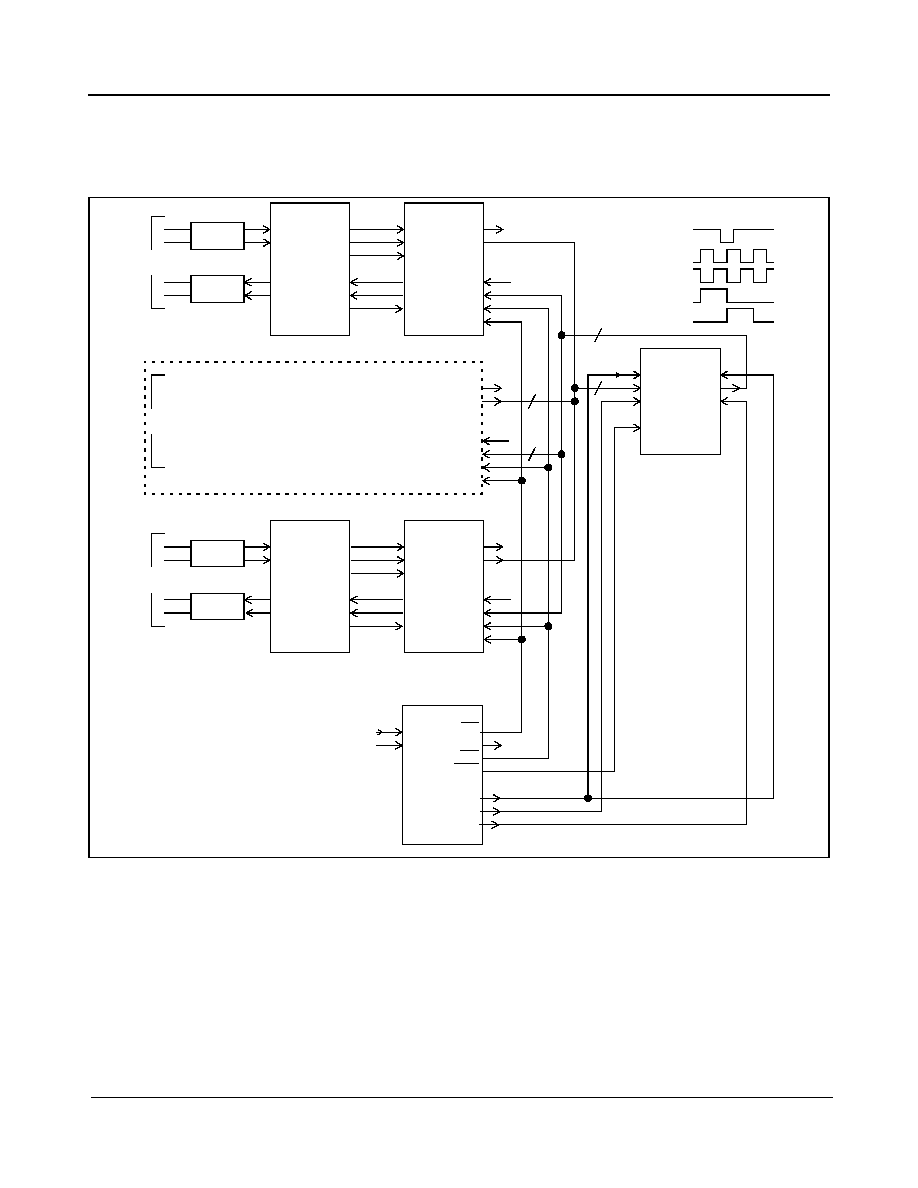
MT9072
Data Sheet
225
Zarlink Semiconductor Inc.
18.0 Applications
18.1 T1 Applications
Figure 11 - 8 T1 Links with Synchronous Common Channel Signaling for up to 24 Channels
RPOS
RNEG
EXCLi
TPOS
TNEG
TXCL
DSTo
CSTo
DSTi
CSTi
CKi
FPi
Framer 1/8
RPOS
RNEG
RCLK
TPOS
TNEG
TCLK
LIU 1/8
RT
RR
TT
TR
Transmit
xfmr
LINE 1
RCLK, TCLK
RSP
TSP
F0
C2
Receive
xfmr
RCLK
RDATA
RSP
SCLK
TCLK
TDATA
TSP
HDLC
PRI
SEC
F0o
C2o
C4o
C16o
RCLK
RSP
TSP
PLL
From RCLK's
of LIU's
Notes:
Framer 1-8, 1 of MT9072
LIU 1-8, * of Generic LIU
PLL, 1 of MT9044
HDLC, 1 of PEB 20320
(MUNICH 32)
- Framer elastic buffer is used.
- LIU Transmit JA and PLL are bypassed.
RPOS
RNEG
EXCLi
TPOS
TNEG
TXCL
DSTo
CSTo
DSTi
CSTi
CKi
FPi
Framer 8/8
RPOS
RNEG
RCLK
TPOS
TNEG
TCLK
LIU 8/8
RT
RR
TT
TR
Transmit
xfmr
LINE 8
Receive
xfmr
LINES 2 to 7
HDLC Timing
Framers 2 to 7
DSTo
CSTo
DSTi
CSTi
CKi
FPi
LIU's 2 to 7
6
6
1
1
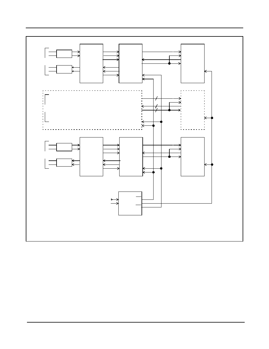
MT9072
Data Sheet
226
Zarlink Semiconductor Inc.
Figure 12 - 8 T1 Links with Synchronous Data Link Signaling
RPOS
RNEG
RCLK
TPOS
TNEG
TCLK
LIU 1/8
RT
RR
TT
TR
Transmit
xfmr
LINE 1
Receive
xfmr
PRI
SEC
F0o
C2o
C4o
PLL
From RCLK's
of LIU's
Notes:
Framer 1-8, 1 of MT9072
LIU 1-8, 8 of Generic LIU's
PLL, 1 of MT9042
HDLC, 8 of MT8952
- Framer elastic buffer is used.
- Data Link data passes through the elastic
buffer.
- TxDLC outputs an enable signal
- LIU Transmit JA and PLL are bypassed.
- The MT8952B is in External Timing mode.
RPOS
RNEG
RCLK
TPOS
TNEG
TCLK
LIU 8/8
RT
RR
TT
TR
Transmit
xfmr
LINE 8
Receive
xfmr
LINES 2 to 7
Framers 2 to 7
DSTo
TxDL
TxDLC
CKi
FPi
LIU's 2 to 7
6
6
CDSTi
RxCEN
CDSTo
TxCEN
CKi
HDLC 1/8
6
CDSTi
RxCEN
CDSTo
TxCEN
CKi
HDLC 2 to 7
CDSTi
RxCEN
CDSTo
TxCEN
CKi
HDLC 8/8
RPOS
RNEG
EXCLi
TPOS
TNEG
TXCL
DSTo
TxDL
TxDLC
CKi
FPi
Framer 1/8
RPOS
RNEG
EXCLi
TPOS
TNEG
TXCL
DSTo
TxDL
TxDLC
CKi
FPi
Framer 8/8
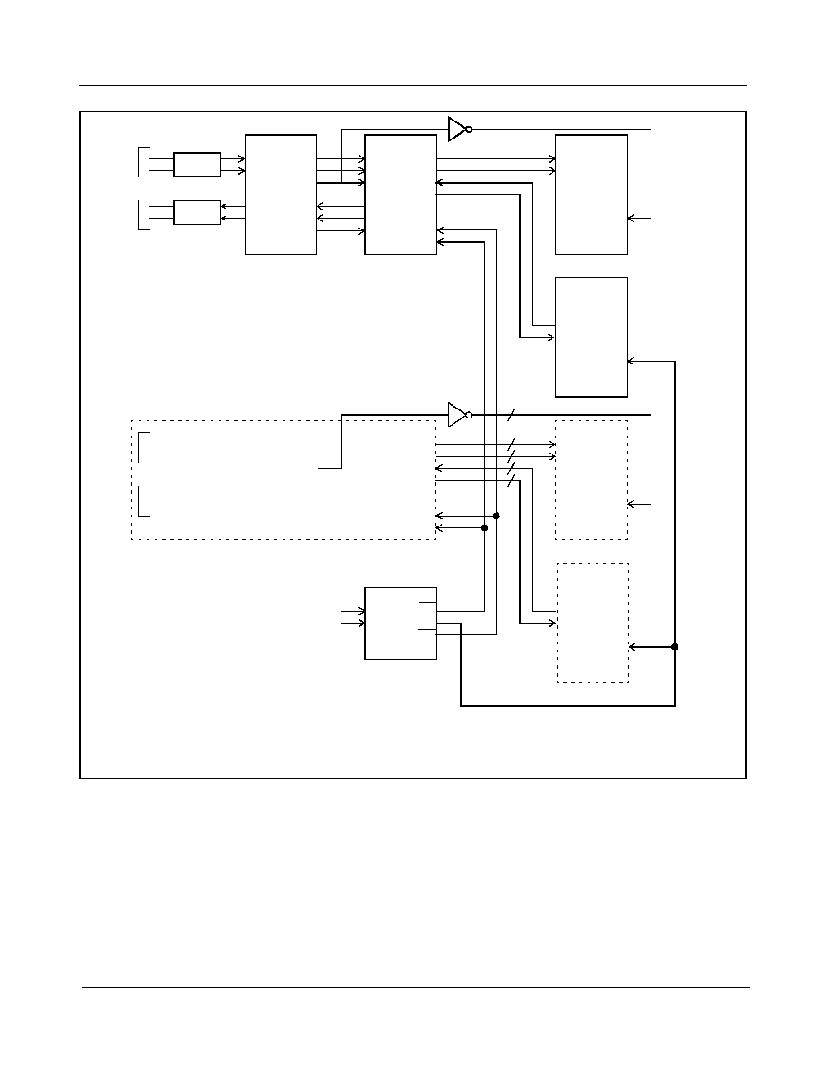
MT9072
Data Sheet
227
Zarlink Semiconductor Inc.
Figure 13 - 8 T1 Links with Asynchronous Data Link Signaling
Notes:
Framer 1-8, 1 of MT9072
LIU 1-8, 8 of Generic LIU
PLL, 1 of MT9042
HDLC, 8 of MT8952
- Framer elastic buffer is used.
- Data Link data passes through the elastic
buffer.
- TxDLC & RXDLC outputs an enable signal
- LIU Transmit JA and PLL are bypassed.
- The MT8952B is in External Timing mode.
RPOS
RNEG
RCLK
TPOS
TNEG
TCLK
LIU 1/8
RT
RR
TT
TR
Transmit
xfmr
LINE 1
Receive
xfmr
PRI
SEC
F0o
C2o
C4o
PLL
From RCLK's
of LIU's
LINES 2 to 7
Framers 2 to 7
RxDL
RxDLC
TxDL
TxDLC
CKi
FPi
LIU's 2 to 7
6
RPOS
RNEG
EXCLi
TPOS
TNEG
TXCL
RxDL
RxDLC
TxDL
TxDLC
CKi
FPi
Framer 1/8
CDSTi
RxCEN
CDSTo
TxCEN
CKi
HDLC 1/16
6
CDSTi
RxCEN
CDSTo
TxCEN
CKi
HDLC 3-15 odd
CDSTi
RxCEN
CDSTo
TxCEN
CKi
HDLC 2/16
CDSTi
RxCEN
CDSTo
TxCEN
CKi
HDLC 4-16 even
6
6
RCLK
6

MT9072
Data Sheet
228
Zarlink Semiconductor Inc.
Figure 14 - 8 T1 Links with no JA or PLL in LIU, Slave or Master Mode, Jitter-Free ST-BUS
RPOS
RNEG
EXCLi
TPOS
TNEG
TXCL
DSTo
CSTo
DSTi
CSTi
CKi
FPi
Framer 1/8
RPOS
RNEG
RCLK
TPOS
TNEG
TCLK
LIU 1/8
RT
RR
TT
TR
Transmit
xfmr
LINE 1
Receive
xfmr
From RCLK's
of LIU's
Notes:
Framer 1-8, 1 of MT9072
LIU 1-8, 8 of Generic LIU
PLL, 1 of MT9042
LDX, 1 of MT90820
- Framer elastic buffer is used.
- LIU Transmit JA and PLL are bypassed.
RPOS
RNEG
RCLK
TPOS
TNEG
TCLK
LIU 8/8
RT
RR
TT
TR
Transmit
xfmr
LINE 8
Receive
xfmr
LINES 2 to 7
Framers 2 to 7
DSTo
CSTo
DSTi
CSTi
CKi
FPi
LIU's 2 to 7
STi0
STo0
STi1-6
STo1-6
STi7
STo7
STi8-15
STo8-15
F0i
C4i
LDX
7
7
PRI
SEC
F0o
C2o
C4o
PLL
RPOS
RNEG
EXCLi
TPOS
TNEG
TXCL
DSTo
CSTo
DSTi
CSTi
CKi
FPi
Framer 8/8
RXDLC
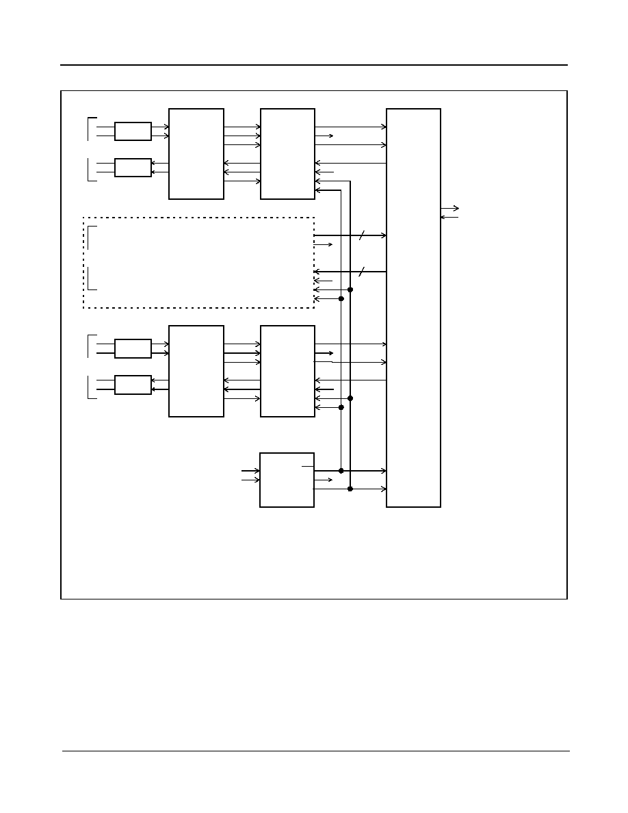
MT9072
Data Sheet
229
Zarlink Semiconductor Inc.
Figure 15 - 8 T1 Links with ATM IMA with Synchronous ST-BUS Mode
RPOS
RNEG
RCLK
TPOS
TNEG
TCLK
LIU 1/8
RT
RR
TT
TR
Transmit
xfmr
LINE 1
Receive
xfmr
From RCLK's
of LIU's
Notes:
Framer 1-8, 1 of MT9072
LIU 1-8, 8 of Generic LIU
PLL, 1 of MT9042
ATM IMA
- Framer elastic buffer is used.
- LIU Transmit JA and PLL are
bypassed.
RPOS
RNEG
RCLK
TPOS
TNEG
TCLK
LIU 8/8
RT
RR
TT
TR
Transmit
xfmr
LINE 8
Receive
xfmr
LINES 2 to 7
Framers 2 to 7
DSTo
CSTo
DSTi
CSTi
CKi
FPi
LIU's 2 to 7
DSTi0
DSTo0
DSTi 1-6
DSTo1-6
DSTi7
SSTo7
RxSYNCi
RxCKi
IMA
7
7
PRI
SEC
F8o
C2o
C1.5o
PLL
ATM BUS
RPOS
RNEG
EXCLi
TPOS
TNEG
TXCL
DSTo
CSTo
DSTi
CSTi
CKi
FPi
Framer 1/8
RPOS
RNEG
EXCLi
TPOS
TNEG
TXCL
DSTo
CSTo
DSTi
CSTi
CKi
FPi
Framer 8/8
RxDLC
RxDLC
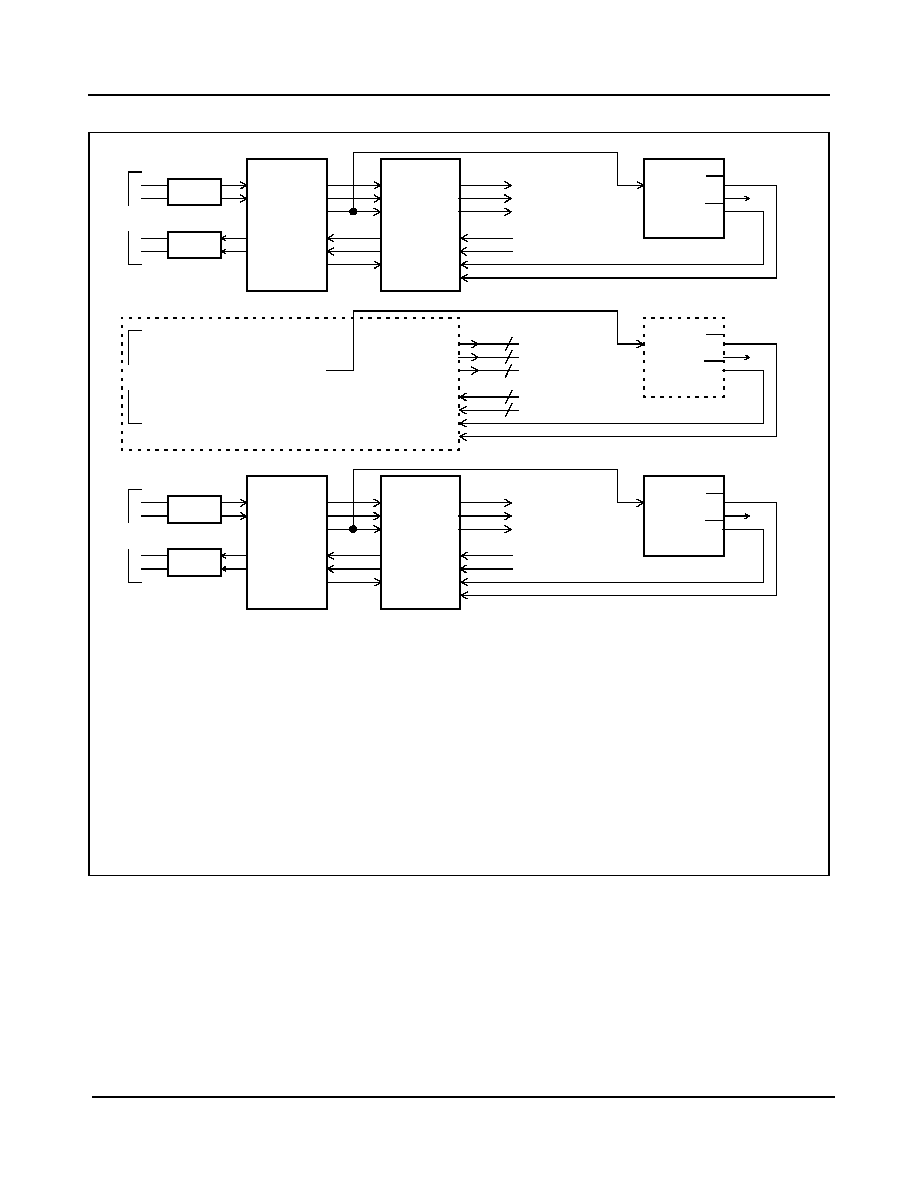
MT9072
Data Sheet
230
Zarlink Semiconductor Inc.
Figure 16 - 8 T1 Links with Asynchronous ST-BUS
RPOS
RNEG
EXCLi
TPOS
TNEG
TXCL
DSTo
CSTo
RxDL
DSTi
CSTi
CKi
FPi
Framer 1/8
RPOS
RNEG
RCLK
TPOS
TNEG
TCLK
LIU 1/8
RT
RR
TT
TR
Transmit
xfmr
LINE 1
Receive
xfmr
Notes:
Framer 1-8, 1 of MT9072
LIU 1-8, 8 of Generic LIU
PLL, 8 of MT9041
- Framer elastic buffer is optional with DSTo and
CSTo.
- Framer elastic buffer is not used with RxDL.
- LIU Transmit JA and PLL are bypassed.
RPOS
RNEG
RCLK
TPOS
TNEG
TCLK
LIU 8/8
RT
RR
TT
TR
Transmit
xfmr
LINE 8
Receive
xfmr
LINES 2 to 7
Framers 2 to 7
DSTo
CSTo
RxDL
DSTi
CSTi
CKi
FPi
LIU's 2 to 7
PRI
F0o
C2o
C4o
PLL 1/8
RCLK
PRI
F0o
C2o
C4o
PLL 2 to 7
PRI
F0o
C2o
C4o
PLL 8/8
RPOS
RNEG
EXCLi
TPOS
TNEG
TXCL
DSTo
CSTo
RxDL
DSTi
CSTi
CKi
FPi
Framer 8/8
6
6
6
6
6

MT9072
Data Sheet
231
Zarlink Semiconductor Inc.
18.2 E1 Applications
Figure 17 - 8 E1 Links with ATM IMA with Asynchronous ST-BUS Mode
RPOS
RNEG
EXCLi
TPOS
TNEG
TXCL
DSTo
RxDLC
RxBF
DSTi
CKi
FPi
Framer 1/8
RPOS
RNEG
RCLK
TPOS
TNEG
TCLK
LIU 1/8
RT
RR
TT
TR
Transmit
xfmr
LINE 1
Receive
xfmr
Notes:
Framer 1-8, 1 of MT9072
LIU 1-8, 8 of Generic LIU
PLL, 1 of MT9042
IMA
- Framer elastic buffer is bypassed at DSTo.
- LIU Transmit JA and PLL are enabled.
- Transmit and receive paths may be asynchronous with each
other.
RPOS
RNEG
RCLK
TPOS
TNEG
TCLK
LIU 8/8
RT
RR
TT
TR
Transmit
xfmr
LINE 8
Receive
xfmr
LINES 2 to 7
Framers 2 to 7
DSTo
RxDLC
RxBF
DSTi
CKi
FPi
LIU's 2 to 7
DSTi0
RxCK0
RxSYNC0
DSTo0
TxCK0
TxSYNC0
DSTi 1-6
RxCK1-6
RxSYNC1-6
DSTo1-6
TxCK1-6
TxSYNC1-6
DSTi7
RxCK7
RxSYNC7
DSTo7
TxCK7
TxSYNC7
PLLREF0
PLLREF1
REFCK0
IMA
PRI
SEC
F0o
C2o
C4o
PLL
ATM BUS
F0
C1.5i
GCI Timing
F0 = FPi = TxSYNCo
F0 = RxBF = RxSYNCo
C1.5 = RxDLC = RxCKo
c1.5i= CKi = TxCKo
Bits
6
6
6
6
6
6
RPOS
RNEG
EXCLi
TPOS
TNEG
TXCL
DSTo
RxDLC
RxBF
DSTi
CKi
FPi
Framer 8/8

MT9072
Data Sheet
232
Zarlink Semiconductor Inc.
Figure 18 - 8 E1 Links with Synchronous Common Channel Signaling for up to 24 Channels
RPOS
RNEG
E2i
TPOS
TNEG
T2o
DSTo
CSTo
DSTi
CSTi
CKi
FPi
Framer 1/8
RPOS
RNEG
RCLK
TPOS
TNEG
TCLK
LIU 1/8
RT
RR
TT
TR
Transmit
xfmr
LINE 1
RCLK, TCLK
RSP
TSP
F0
C2
Receive
xfmr
RCLK
RDATA
RSP
SCLK
TCLK
TDATA
TSP
HDLC
PRI
SEC
F0o
C2o
C4o
C16o
RCLK
RSP
TSP
PLL
From RCLK's
of LIU's
Notes:
Framer 1-8, 1 of MT9072
LIU 1-8, of Generic LIU
PLL, 1 of MT9044
HDLC, 1 of PEB 20320
(MUNICH 32)
- Framer elastic buffer is used.
- LIU Transmit JA and PLL are bypassed.
RPOS
RNEG
E2i
TPOS
TNEG
T2o
DSTo
CSTo
DSTi
CSTi
CKi
FPi
Framer 8/8
RPOS
RNEG
RCLK
TPOS
TNEG
TCLK
LIU 8/8
RT
RR
TT
TR
Transmit
xfmr
LINE 8
Receive
xfmr
LINES 2 to 7
HDLC Timing
Framers 2 to 7
DSTo
CSTo
DSTi
CSTi
CKi
FPi
LIU's 2 to 7
6
6
1
1

MT9072
Data Sheet
233
Zarlink Semiconductor Inc.
Figure 19 - E3 (34 Mb/s) MUX Cross Connect with 16 Asynchronous E1 Links
PRI
SEC
F0o
C2o
C4o
PLL
Notes:
Framer 1-16, 2 of MT9072
LDX, 1 of MT90820
PLL, 1 of MT9042
- Framer elastic buffer is used.
- LIU Transmit JA and PLL are bypassed.
Framers 2 to 15
DSTo
CSTo
DSTi
CSTi
CKi
FPi
RXPOS
RXNEG
R34CK
TXPOS
TXNEG
T34CK
E3 MUX
RPOS
RNEG
RCLK
TPOS
TNEG
TCLK
E3 LIU
RT
RR
TT
TR
Transmit
xfmr
E3 LINE
Receive
xfmr
RPOS
RNEG
E2i
TPOS
TNEG
T20
14
14
14
14
STi0
STo0
STi1-14
STo1-14
STi15
STo15
F0i
C4i
LDX
14
14
RPOS
RNEG
RCLK
TPOS
TNEG
TCLK
RPOS
RNEG
RCLK
TPOS
TNEG
TCLK
RPOS
RNEG
RCLK
TPOS
TNEG
TCLK
14
14
From RCLK's
of E3 MUX
RPOS
RNEG
E2i
TPOS
TNEG
T2o
DSTo
CSTo
DSTi
CSTi
CKi
FPi
Framer 1/16
RPOS
RNEG
E2i
TPOS
TNEG
T2o
DSTo
CSTo
DSTi
CSTi
CKi
FPi
Framer 1/16

MT9072
Data Sheet
234
Zarlink Semiconductor Inc.
Figure 20 - E3 (34 Mb/s) MUX Concentrator to 16 Asynchronous E1 Links
Notes:
LIU 1-8, 8 of Generic LIU
- LIU Transmit JA and PLL are not bypassed.
RXPOS
RXNEG
R34CK
TXPOS
TXNEG
T34CK
E3 MUX
RPOS
RNEG
RCLK
TPOS
TNEG
TCLK
E3 LIU
RT
RR
TT
TR
Transmit
xfmr
E3 LINE
Receive
xfmr
14
14
14
14
RPOS
RNEG
RCLK
TPOS
TNEG
TCLK
RPOS
RNEG
RCLK
TPOS
TNEG
TCLK
RPOS
RNEG
RCLK
TPOS
TNEG
TCLK
14
14
TPOS
TNEG
TCLK
RPOS
RNEG
RCLK
LIU 1/16
TT
TR
RT
RR
Transmit
xfmr
LINE 1
Receive
xfmr
TPOS
TNEG
TCLK
RPOS
RNEG
RCLK
LIU 16/16
TT
TR
RT
RR
Transmit
xfmr
LINE 16
Receive
xfmr
TPOS
TNEG
TCLK
RPOS
RNEG
RCLK
LIU 2-15
TT
TR
RT
RR
Transmit
xfmr
LINE 2 to 15
Receive
xfmr

MT9072
Data Sheet
235
Zarlink Semiconductor Inc.
Figure 21 - 8 E1 Links with Synchronous Data Link Signaling
RPOS
RNEG
RCLK
TPOS
TNEG
TCLK
LIU 1/8
RT
RR
TT
TR
Transmit
xfmr
LINE 1
Receive
xfmr
PRI
SEC
F0o
C2o
C4o
PLL
From RCLK's
of LIU's
Notes:
Framer 1-8, 1 of MT9072
LIU 1-8, 4 of Generic LIU
PLL, 1 of MT9042
HDLC, 8 of MT8952
- Framer elastic buffer is used.
- Data Link data passes through the elastic buffer.
- TxDLC outputs an enable signal
- LIU Transmit JA and PLL are bypassed.
- The MT8952B is in External Timing mode.
RPOS
RNEG
RCLK
TPOS
TNEG
TCLK
LIU 8/8
RT
RR
TT
TR
Transmit
xfmr
LINE 8
Receive
xfmr
LINES 2 to 7
Framers 2 to 7
DSTo
TxDL
TxDLC
CKi
FPi
LIU's 2 to 7
6
6
CDSTi
RxCEN
CDSTo
TxCEN
CKi
HDLC 1/8
6
CDSTi
RxCEN
CDSTo
TxCEN
CKi
HDLC 2 to 7
CDSTi
RxCEN
CDSTo
TxCEN
CKi
HDLC 8/8
RPOS
RNEG
E2i
TPOS
TNEG
T2o
DSTo
TxDL
TxDLC
CKi
FPi
Framer 1/8
RPOS
RNEG
E2i
TPOS
TNEG
T2o
DSTo
TxDL
TxDLC
CKi
FPi
Framer 8/8

MT9072
Data Sheet
236
Zarlink Semiconductor Inc.
Figure 22 - 8 E1 Links with Asynchronous Data Link Signaling
Notes:
Framer 1-8, 1 of MT9072
LIU 1-8, 8 of Generic LIU
PLL, 1 of MT9042
HDLC, 8 of MT8952
- Framer elastic buffer is used.
- Data Link data passes through the elastic buffer.
- TxDLC & RXDLC outputs an enable signal
- LIU Transmit JA and PLL are bypassed.
- The MT8952B is in External Timing mode.
RPOS
RNEG
RCLK
TPOS
TNEG
TCLK
LIU 1/8
RT
RR
TT
TR
Transmit
xfmr
LINE 1
Receive
xfmr
PRI
SEC
F0o
C2o
C4o
PLL
From RCLK's
of LIU's
LINES 2 to 7
Framers 2 to 7
RxDL
RxDLC
TxDL
TxDLC
CKi
FPi
LIU's 2 to 7
6
RPOS
RNEG
E2i
TPOS
TNEG
T2o
RxDL
RxDLC
TxDL
TxDLC
CKi
FPi
Framer 1/8
CDSTi
RxCEN
CDSTo
TxCEN
CKi
HDLC 1/16
6
CDSTi
RxCEN
CDSTo
TxCEN
CKi
HDLC 3-15 odd
CDSTi
RxCEN
CDSTo
TxCEN
CKi
HDLC 2/16
CDSTi
RxCEN
CDSTo
TxCEN
CKi
HDLC 4-16 even
6
6
RCLK
6

MT9072
Data Sheet
237
Zarlink Semiconductor Inc.
Figure 23 - 8 E1 Links with no JA or PLL in LIU, Slave or Master Mode, Jitter-Free ST-BUS
RPOS
RNEG
E2i
TPOS
TNEG
T2o
DSTo
CSTo
DSTi
CSTi
CKi
FPi
Framer 1/8
RPOS
RNEG
RCLK
TPOS
TNEG
TCLK
LIU 1/8
RT
RR
TT
TR
Transmit
xfmr
LINE 1
Receive
xfmr
From RCLK's
of LIU's
Notes:
Framer 1-8, 1 of MT9072
LIU 1-8, * of Generic LIU
PLL, 1 of MT9042
LDX, 1 of MT90820
- Framer elastic buffer is used.
- LIU Transmit JA and PLL are bypassed.
RPOS
RNEG
RCLK
TPOS
TNEG
TCLK
LIU 8/8
RT
RR
TT
TR
Transmit
xfmr
LINE 8
Receive
xfmr
LINES 2 to 7
Framers 2 to 7
DSTo
CSTo
DSTi
CSTi
CKi
FPi
LIU's 2 to 7
STi0
STo0
STi1-6
STo1-6
STi7
STo7
STi8-15
STo8-15
F0i
C4i
LDX
7
7
PRI
SEC
F0o
C2o
C4o
PLL
RPOS
RNEG
E2i
TPOS
TNEG
T2o
DSTo
CSTo
DSTi
CSTi
CKi
FPi
Framer 8/8

MT9072
Data Sheet
238
Zarlink Semiconductor Inc.
Figure 24 - 8 E1 Links with ATM IMA with Synchronous ST-BUS Mode
RPOS
RNEG
RCLK
TPOS
TNEG
TCLK
LIU 1/8
RT
RR
TT
TR
Transmit
xfmr
LINE 1
Receive
xfmr
From RCLK's
of LIU's
Notes:
Framer 1-8, 1 of MT9072
LIU 1-8, 8 of Generic LIU
PLL, 1 of MT9042
IMA
- Framer elastic buffer is used.
- LIU Transmit JA and PLL are bypassed.
RPOS
RNEG
RCLK
TPOS
TNEG
TCLK
LIU 8/8
RT
RR
TT
TR
Transmit
xfmr
LINE 8
Receive
xfmr
LINES 2 to 7
Framers 2 to 7
DSTo
CSTo
DSTi
CSTi
CKi
FPi
LIU's 2 to 7
DSTi0
DSTo0
DSTi 1-6
DSTo1-6
DSTi7
SSTo7
RxSYNCi
RxCKi
IMA
7
7
PRI
SEC
F0o
C2o
C4o
PLL
ATM BUS
RPOS
RNEG
E2i
TPOS
TNEG
T2o
DSTo
CSTo
DSTi
CSTi
CKi
FPi
Framer 1/8
RPOS
RNEG
E2i
TPOS
TNEG
T2o
DSTo
CSTo
DSTi
CSTi
CKi
FPi
Framer 8/8
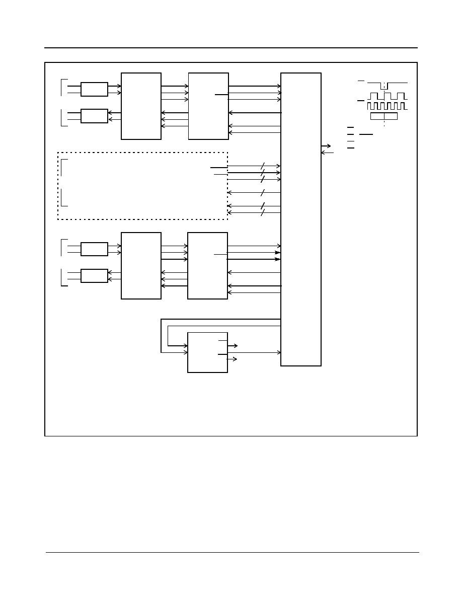
MT9072
Data Sheet
239
Zarlink Semiconductor Inc.
Figure 25 - 8 E1 Links with ATM IMA with Asynchronous ST-BUS Mode
RPOS
RNEG
E2i
TPOS
TNEG
T2o
DSTo
RxDLC
RxBF
DSTi
CKi
FPi
Framer 1/8
RPOS
RNEG
RCLK
TPOS
TNEG
TCLK
LIU 1/8
RT
RR
TT
TR
Transmit
xfmr
LINE 1
Receive
xfmr
Notes:
Framer 1-8, 1 of MT9072
LIU 1-8, 8 of Generic LIU
PLL, 1 of MT9042
IMA
- Framer elastic buffer is bypassed at DSTo.
- LIU Transmit JA and PLL are enabled.
- Transmit and receive paths may be asynchronous with each other.
RPOS
RNEG
RCLK
TPOS
TNEG
TCLK
LIU 8/8
RT
RR
TT
TR
Transmit
xfmr
LINE 8
Receive
xfmr
LINES 2 to 7
Framers 2 to 7
DSTo
RxDLC
RxBF
DSTi
CKi
FPi
LIU's 2 to 7
DSTi0
RxCK0
RxSYNC0
DSTo0
TxCK0
TxSYNC0
DSTi 1-6
RxCK1-6
RxSYNC1-6
DSTo1-6
TxCK1-6
TxSYNC1-6
DSTi7
RxCK7
RxSYNC7
DSTo7
TxCK7
TxSYNC7
PLLREF0
PLLREF1
REFCK0
IMA
PRI
SEC
F0o
C2o
C4o
PLL
ATM BUS
F0
C2
ST-BUS Timing
F0 = FPi = TxSYNCo
F0 = RxBF = RxSYNCo
C4 = RxDLC = RxCKo
C4 = CKi = TxCKo
Bits
C4
6
6
6
6
6
6
RPOS
RNEG
E2i
TPOS
TNEG
T2o
DSTo
RxDLC
RxBF
DSTi
CKi
FPi
Framer 8/8
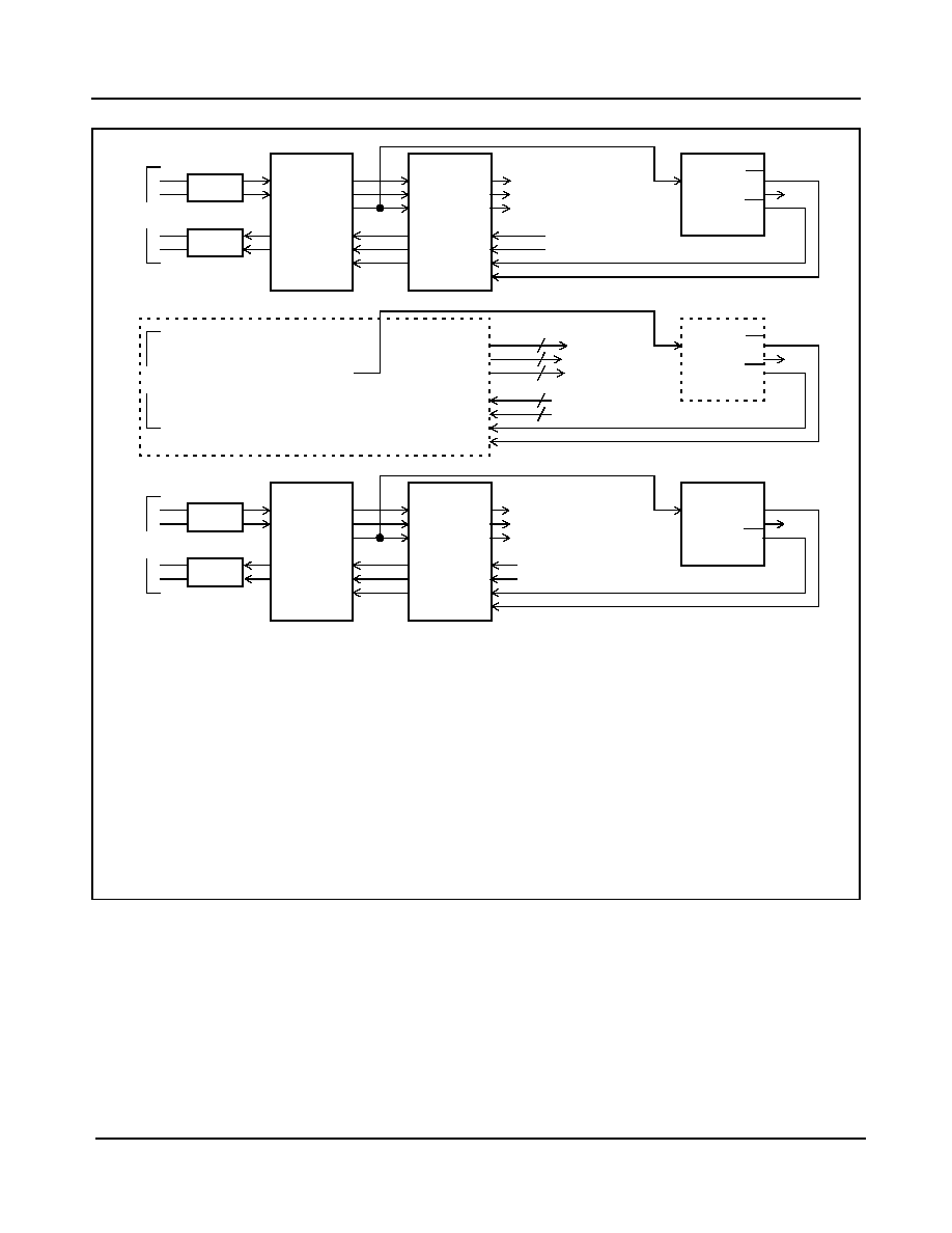
MT9072
Data Sheet
240
Zarlink Semiconductor Inc.
Figure 26 - 8 E1 Links with Asynchronous ST-BUS
RPOS
RNEG
E2i
TPOS
TNEG
T2o
DSTo
CSTo
RxDL
DSTi
CSTi
CKi
FPi
Framer 1/8
RPOS
RNEG
RCLK
TPOS
TNEG
TCLK
LIU 1/8
RT
RR
TT
TR
Transmit
xfmr
LINE 1
Receive
xfmr
Notes:
Framer 1-8, 1 of MT9072
LIU 1-8, * of Generic LIU
PLL, 8 of MT9041
- Framer elastic buffer is optional with DSTo and CSTo.
- Framer elastic buffer is not used with RxDL.
- LIU Transmit JA and PLL are bypassed.
RPOS
RNEG
RCLK
TPOS
TNEG
TCLK
LIU 8/8
RT
RR
TT
TR
Transmit
xfmr
LINE 8
Receive
xfmr
LINES 2 to 7
Framers 2 to 7
DSTo
CSTo
RxDL
DSTi
CSTi
CKi
FPi
LIU's 2 to 7
PRI
F0o
C2o
C4o
PLL 1/8
RCLK
PRI
F0o
C2o
C4o
PLL 2 to 7
PRI
F0o
C2o
C4o
PLL 8/8
RPOS
RNEG
E2i
TPOS
TNEG
T2o
DSTo
CSTo
RxDL
DSTi
CSTi
CKi
FPi
Framer 8/8
6
6
6
6
6

MT9072
Data Sheet
241
Zarlink Semiconductor Inc.
19.0 AC/DC Electrical Characteristics
19.1 General
* Voltages are with respect to ground (VSS) unless otherwise stated.
* Exceeding these values may cause permanent damage. Functional operation under these conditions is not implied.
Characteristics are for clocked operation over the ranges of recommended operating temperature and supply voltage.
Typical figures are at 25�C and are for design aid only: not guaranteed and not subject to production testing.
Absolute Maximum Ratings*
Parameter
Symbol
Min.
Max.
Units
1
Supply Voltage
V
DD
-0.3
5.5
V
2
Voltage at Digital Inputs
V
I
-0.3
V
DD
+ 0.3
V
3
Current at Digital Inputs
I
I
30
mA
4
Voltage at Digital Outputs
V
O
-0.3
V
DD
+ 0.3
V
5
Current at Digital Outputs
I
O
30
mA
6
Storage Temperature
T
ST
-65
150
�C
Recommended Operating Conditions* -
Voltages are with respect to ground (VSS) unless otherwise stated
Characteristics
Sym.
Min.
Typ.
Max.
Units
Test Conditions
1
Operating Temperature
T
OP
-40
25
85
�C
2
Supply Voltage
V
DD
3.0
3.3
3.6
V
DC Electrical Characteristics
-
Voltages are with respect to ground (VSS) unless otherwise stated
Characteristics
Sym.
Min.
Typ.
Max.
Units
Test Conditions
1
Supply Current
I
DD
30
mA
Outputs unloaded.
Transmitting an all 1's
signal.
2
Input High Voltage (Digital Inputs)
V
IH
2.0
V
DD
V
3
Input Low Voltage (Digital Inputs)
V
IL
0
0.8
V
4
Input Leakage (Digital Inputs)
I
IL
1
10
�A
V
I
= 0 to V
DD
5
Output High Voltage (Digital
Outputs)
V
OH
2.4
V
DD
V
I
OH
= 7 mA @ V
OH
= 2.4 V
6
Output High Current (Digital
Outputs)
I
OH
7
mA
Source V
OH
=2.4 V
7
Output Low Voltage (Digital Outputs)
V
OL
V
SS
0.4
V
I
OL
= 2 mA @ V
OL
= 0.4 V
8
Output Low Current (Digital Outputs)
I
OL
2
mA
Sink V
OL
= 0.4 V
9
High Impedance Leakage (Digital
I/O)
I
OZ
1
10
�A
V
O
= 0 to V
DD

MT9072
Data Sheet
242
Zarlink Semiconductor Inc.
* Timing for output signals is based on the worst case result of the combination of TTL and CMOS thresholds.
Figure 27 - Timing Parameter Measurement Voltage Levels
Typical figures are at 25�C and are for design aid only: not guaranteed and not subject to production testing.
Note 1. High impedance is measured by pulling to the appropriate rail with R
L
, with timing corrected to cancel time taken to discharge C
L
.
AC Electrical Characteristics - Timing Parameter Measurement Voltage Levels* -
Voltages are with respect to
ground (VSS) unless otherwise stated.
Characteristics
Sym.
Level
Units
Conditions/Notes
1
Threshold Voltage
V
T
1.5
0.5
V
DD
V
V
TTL
CMOS
2
Rise/Fall Threshold Voltage High
V
HM
2.0
0.7
V
DD
V
V
TTL
CMOS
3
Rise/Fall Threshold Voltage Low
V
LM
0.8
0.3
V
DD
V
V
TTL
CMOS
AC Electrical Characteristics - Motorola Microprocessor Timing*
Characteristics
Sym.
Min.
Typ.
Max.
Units
Test Conditions
1
DS low
t
DSL
115
ns
2
DS High
t
DSH
50
ns
3
CS Setup
t
CSS
0
ns
4
CS Hold
t
CSH
0
ns
5
R/W Setup
t
RWS
15
ns
6
R/W Hold
t
RWH
0
ns
7
Address Setup
t
ADS
15
ns
8
Address Hold
t
ADH
40
ns
9
Data Delay Read
t
DDR
100
ns
C
L
= 150 pF, R
L
= 1 k
10
Data Hold Read
t
DHR
5
ns
C
L
= 150 pF, R
L
= 1 k
11
Data Active to High Z Delay
t
DAZ
50
ns
C
L
= 150 pF, R
L
= 1 k
,
Note 1
12
Data Setup Write
t
DSW
15
ns
13
Data Hold Write
t
DHW
25
ns
14
Cycle Time
t
CYC
165
ns
ALL SIGNALS
t
IRF,
t
ORF
Timing Reference Points
V
T
V
HM
V
LM
t
IRF,
t
ORF
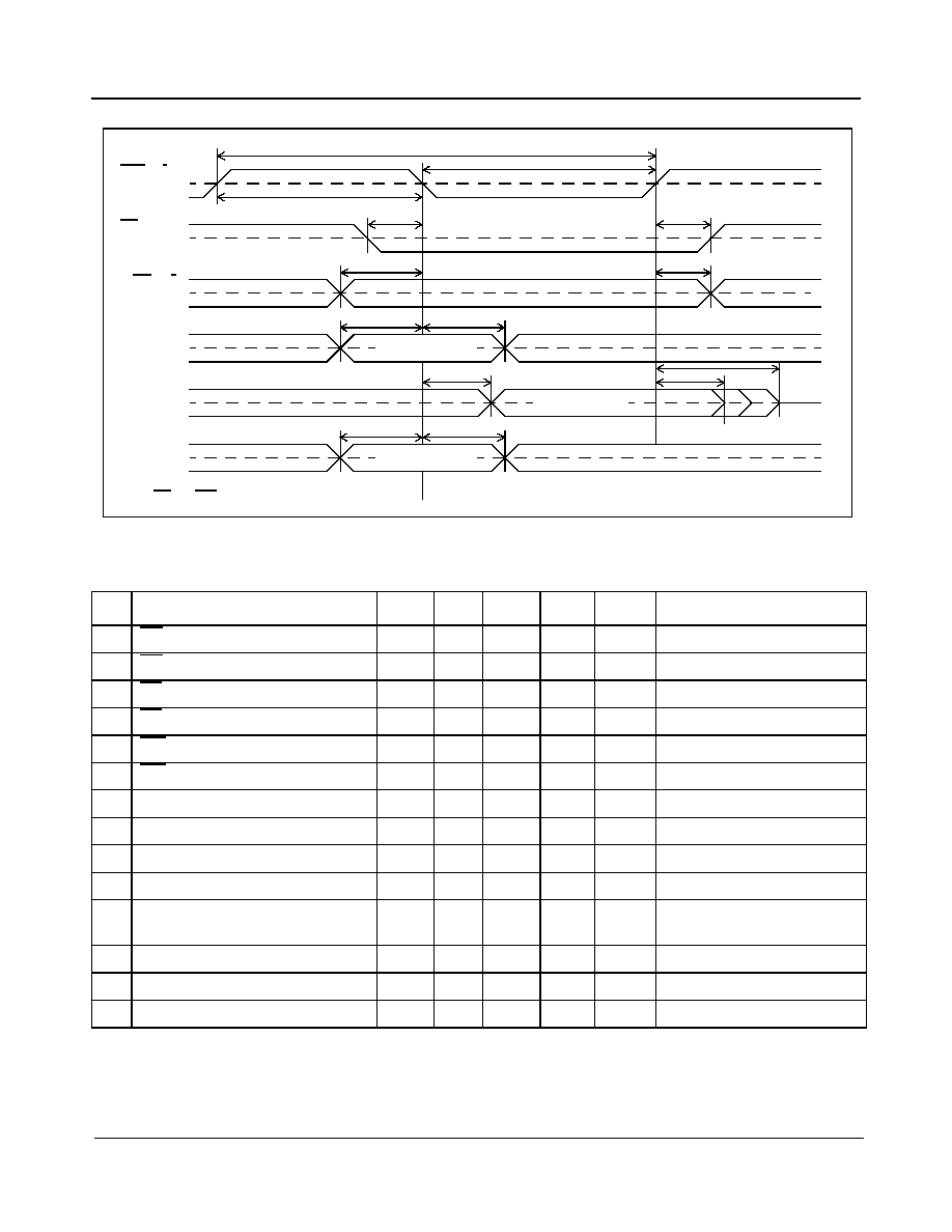
MT9072
Data Sheet
243
Zarlink Semiconductor Inc.
Figure 28 - Motorola Microprocessor Timing
Typical figures are at 25�C and are for design aid only: not guaranteed and not subject to production testing.
Note 1. High impedance is measured by pulling to the appropriate rail with R
L
, with timing corrected to cancel time taken to discharge C
L
.
AC Electrical Characteristics - Intel Microprocessor Timing*
Characteristics
Sym.
Min.
Typ.
Max.
Units
Test Conditions
1
RD low
t
RDL
115
ns
2
RD High
t
RDH
50
ns
3
CS Setup
t
CSS
0
ns
4
CS Hold
t
CSH
0
ns
5
WR low
t
WRL
70
ns
6
WR High
t
WRH
50
ns
7
Address Setup
t
ADS
15
ns
8
Address Hold
t
ADH
40
ns
9
Data Delay Read
t
DDR
100
ns
C
L
= 150 pF, R
L
= 1 k
.
10
Data Hold Read
t
DHR
5
ns
C
L
= 150 pF, R
L
= 1 k
11
Data Active to High Z Delay
t
DAZ
50
ns
C
L
= 150 pF, R
L
= 1 k
, Note
1
12
Data Setup Write
t
DSW
15
ns
13
Data Hold Write
t
DHW
25
ns
14
Cycle Time
t
CYC
165
MT9072
Outputs Data
t
CSS
t
RWS
t
ADS
t
CSH
t
RWH
t
ADH
t
DHR
t
DDR
t
DSH
t
DSL
t
DAZ
Note: DS and CS may be connected together.
t
CYC
V
T
V
T
V
T
V
T
V
T
T
MT9072
Inputs Address
DS (RD)
CS
R/W (WR)
A0-10
D0-15
READ
V
MT9072
InputsData
D0-15
WRITE
t
DSW
t
DSH
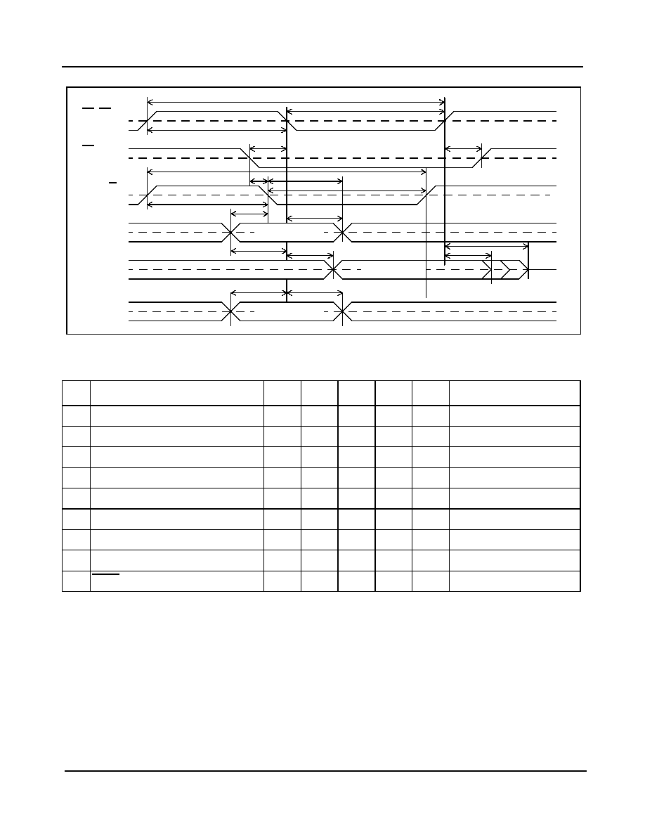
MT9072
Data Sheet
244
Zarlink Semiconductor Inc.
Figure 29 - Intel Microprocessor Timing
AC Electrical Characteristics - JTAG Port Timing
Characteristic
Sym.
Min.
Typ.
Max.
Units
Test Conditions
1
TCK period width
t
TCLK
100
ns
BSDL spec's 12 MHz
2
TCK period width LOW
t
TCLKL
40
ns
3
TCK period width HIGH
t
TCLKH
40
ns
TDI setup time to TCK rising
t
DISU
12
TDI hold time after TCK rising
t
DIH
12
TMS setup time to TCK rising
t
MSSU
12
TMS hold time after TCK rising
t
MSH
12
TDO delay from TCK falling
t
DOD
50
TRST pulse width
t
TRST
25
MT9072
Outputs Data
t
CSS
t
ADS
t
CSH
t
ADH
t
DSW
t
DHR
t
DDR
t
DHW
t
RDH
t
RDL
t
DAZ
t
CYC
V
T
V
T
V
T
V
T
V
T
MT9072
Inputs Address
t
ADS
t
ADH
t
WRH
t
WRH
t
CYC
t
CSS
RD (DS)
CS
WR (R/W)
A0-10
D0-15
READ
V
T
MT9072
Inputs Data
D0-D15
WRITE
t
DSW
t
DSH
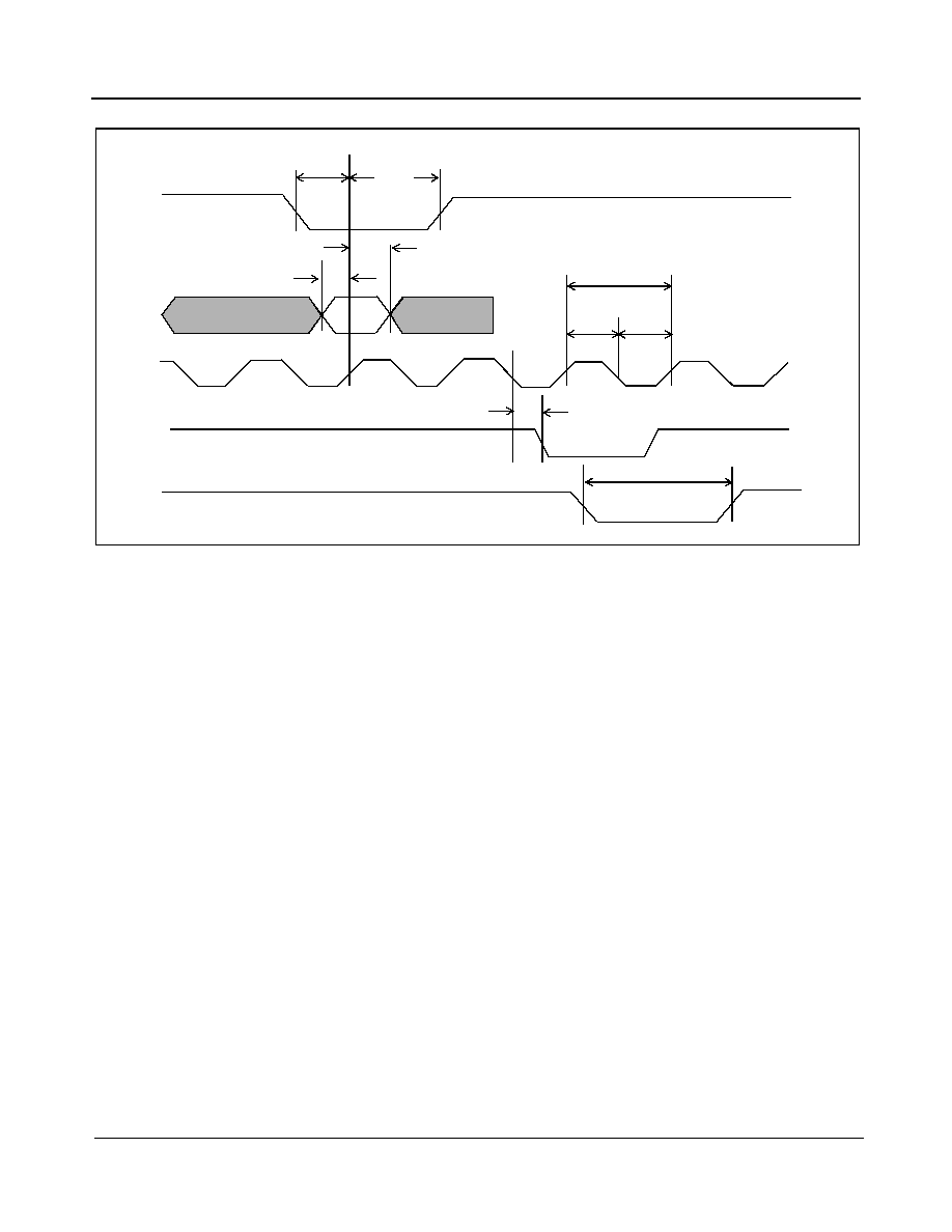
MT9072
Data Sheet
245
Zarlink Semiconductor Inc.
Figure 30 - JTAG Port Timing
t
mssu
TDI
TDO
TMS
TCK
t
disu
t
msh
t
dih
t
dod
t
tclkh
t
tclkl
t
tclk
TRST
t
trst

MT9072
Data Sheet
246
Zarlink Semiconductor Inc.
Figure 31 - GCI 2.048 Mb/s Factional Timing Diagram
Figure 32 - GCI 2.048 Mb/s Timing Diagram
AC Electrical Characteristics - GCI 2.048Mb/sTiming (T1 and E1)
Characteristics
Sym.
Min.
Typ.
Max.
Units
Test Conditions
1
DCL Clock Width High or Low
t
DCLW
100
122
144
ns
2
Frame Pulse Setup
t
FSCS
50
ns
3
Frame Pulse Hold
t
FSCH
50
ns
4
Serial Input Setup
t
SIS
30
ns
5
Serial Input Hold
t
SIH
50
ns
6
Serial Output Delay
t
SOD
125
ns
150 pF load on CSTo and
DSTo
Timeslot 31
Bit 0
Timeslot 0
Bit 7
Timeslot 0
Bit 6
Timeslot 0
Bit 5
CKi
(GCI DCLi)
FPi
(GCI FSCi)
Internal
(ST-BUS C2)
GCI
Bit Cells
2 Mb/s
MT9072
Outputs Data
MT9072
Inputs Data
MT9072
Inputs Data
MT9072
Outputs Data
Timeslot 0
Bit 7
Timeslot 31
Bit 0
V
T
V
T
t
SIH
t
SIS
V
T
t
FSCS
t
FSCH
t
SOD
t
DCLW
t
DCLW
V
T
CKi
(GCI DCLi)
FPi
(GCI FSCi)
GCI
Bit Cells
2 Mb/s
CSTi & DSTi
(Inputs)
CSTo & DSTo
(Outputs)

MT9072
Data Sheet
247
Zarlink Semiconductor Inc.
Figure 33 - ST-BUS 2.048 Mb/s Functional Timing Diagram
Figure 34 - ST-BUS 2.048 Mb/s Timing
AC Electrical Characteristics - ST-BUS 2.048 Mb/s Timing (T1 and E1)
Characteristics
Sym.
Min.
Typ.
Max.
Units
Test Conditions
1
C2i Clock Width High or Low
t
C2W
222
244
266
ns
2
C4i Clock Width High or Low
t
C4W
100
122
144
ns
3
Frame Pulse Setup
t
FPS
50
ns
4
Frame Pulse Hold
t
FPH
50
ns
6
Serial Input Setup
t
SIS
30
ns
7
Serial Input Hold
t
SIH
50
ns
8
Serial Output Delay
t
SOD
90
125
ns
150 pF load on CSTo and
DSTo
Timeslot 31
Bit 0
Timeslot 0
Bit 7
Timeslot 0
Bit 6
Timeslot 0
Bit 5
CKi
(ST-BUS C4i)
FPi
(ST-BUS F0i)
CKi
(ST-BUS C2i)
ST-BUS
Bit Cells
2 Mb/s
MT9072
Outputs Data
MT9072
Inputs Data
MT9072
Inputs Data
MT9072
Outputs Data
Timeslot 0
Bit 7
Timeslot 31
Bit 0
V
T
V
T
t
SIH
t
SIS
V
T
t
FPS
t
FPH
t
SOD
t
C4W
t
C4W
V
T
CKi
(ST-BUS C4i)
FPi
(ST-BUS F0i)
ST-BUS
Bit Cells
2 Mb/s
CSTi & DSTi
(Inputs)
(With C4i Clock)
CSTo & DSTo
(Outputs)
t
C2W
t
C2W
CKi
(ST-BUS C2i)
V
T

MT9072
Data Sheet
248
Zarlink Semiconductor Inc.
Figure 35 - ST-BUS 8.192 Mb/s Functional Timing Diagram
Figure 36 - ST-BUS 8.192 Mb/s Timing
AC Electrical Characteristics - ST-BUS 8.192 Mb/s Timing (T1 and E1)
Characteristics
Sym.
Min.
Typ.
Max.
Units
Test Conditions
1
CKi Clock Width High or Low
t
CKW
25
31
35
ns
3
Frame Pulse Setup
t
FPS
10
60
ns
4
Frame Pulse Hold
t
FPH
20
60
ns
6
Serial Input Setup
t
SIS
10
ns
7
Serial Input Hold
t
SIH
20
ns
8
Serial Output Delay
t
SOD
55
ns
150 pF load on CSTo and
DSTo
Timeslot 127
Bit 0
Timeslot 0
Bit 7
Timeslot 0
Bit 6
Timeslot 0
Bit 5
ST-BUS
Bit Cells
8 Mb/s
CKi
(ST-BUS C16i)
FPi
(ST-BUS F16i)
MT9072
Inputs Data
MT9072
Inputs Data
MT9072
Outputs Data
MT9072
Outputs Data
Timeslot 0
Bit 7
Timeslot 127
Bit 0
V
T
V
T
t
SIH
t
SIS
V
T
t
FPS
t
FPH
t
SOD
t
CKW
t
CKW
V
T
CKi
(ST-BUS C16i)
FPi
(ST-BUS F16i)
CSTi & DSTi
(Inputs)
CSTo & DSTo
(Outputs)
ST-BUS
Bit Cells
8 Mb/s

MT9072
Data Sheet
249
Zarlink Semiconductor Inc.
Figure 37 - ST-BUS 8.192 Mb/s Functional Timing Diagram for CSTo/CSTi CAS
Figure 38 - ST-BUS 8.192 Mb/s Functional Timing Diagram for CSTo/CSTi CCS
19.2 T1 Mode
AC Electrical Characteristics - IMA BackplaneTiming
Characteristics
Sym.
Min.
Typ.
Max.
Units
Test Conditions
1
C1.5i Clock Width High or Low
t
C1.5W
295
324
353
ns
2
Frame Pulse Setup
t
FPS
50
ns
3
Frame Pulse Hold
t
FPH
50
ns
4
Serial Input Setup
t
SIS
30
ns
5
Serial Input Hold
t
SIH
50
ns
6
Clock output delay
t
cod
50
ns
7
Serial Output Delay
t
SOD
20
90
125
ns
150 pF load on CSTo and
DSTo
Timeslot 127
Bit 0
Channel
0
Channel
1
Channel
2
ST-BUS Bit Cells
8 Mb/s
FPi
(ST-BUS F16i)
Channel
3
Chan 0
Data
Chan 1
Data
Chan 2
Data
Chan 0
Data
Chan 1
Data
Chan 2
Data
CSTi0
CSTo0
Note: In Cas only the lower nibble of the stream is used
Note: The ABCD bits are bit 3 to bit 0 respectively
Timeslot 127
Bit 0
Channel
0
Channel
1
Channel
2
ST-BUS Bit Cells
8 Mb/s
FPi
(ST-BUS F16i)
Channel
3
Note: In CCS the complete Byte is used in accordance with CCS Map register Y07. Any 3 CSTi/CSTo channels are
CSTo0
CSTo0
CCS
Chan 0
CCS
Chan 1
CCS
Chan 0
CCS
Chan1
used

MT9072
Data Sheet
250
Zarlink Semiconductor Inc.
Figure 39 - IMA Functional Timing Diagram
Figure 40 - IMA Mode Timing Diagram
Timeslot 23
Bit 0
Sbit
Timeslot 0
Bit 7
Timeslot 0
Bit 6
FPi
(Input)
CKi
( Input))
Bit Cells
1.544 Mb/s
RXBF
(Output)
RXDLC
Timeslot 23
Bit 0
Sbit
Timeslot 0
Bit 7
Timeslot 0
Bit 6
DSTi
(input)
RXDLC
(Output)
Timeslot 23
Bit 0
Sbit
Timeslot 0
Bit 7
Timeslot 0
Bit 6
DSTo
(Output)
MT9072
Outputs Data
MT9072
Inputs Data
MT9072
Inputs Data
MT9072
Outputs Data
Sbit
Timeslot 23
Bit 0
V
T
t
SOD
V
T
FPi
Bit Cells
1.544 Mb/s
DSTo
(Outputs)
t
C1.5W
t
C1.5W
CKi
(C1.5i)
V
T
t
SIH
t
SIS
V
T
DSTi
(Inputs)
(With C1.5i Clock)
RXDLC
(Output)
V
T
V
T
RXBF
t
C1.5W
t
C1.5W
tfs
tfh
Note: In IMA Mode The Data(DSTi) is input with respect to CKI and FPi denotes the Sbit. The DSTo is output with respect
to RXDLC clock and RXBF denotes the S bit. RXDLC is the delayed version of EXCLi.
EXCLi
(Input)
V
T
cod

MT9072
Data Sheet
251
Zarlink Semiconductor Inc.
Figure 41 - Transmit Multiframe Functional Timing
Figure 42 - Transmit MultiframeTiming
AC Electrical Characteristics - Transmit Multiframe Timing
Characteristics
Sym.
Min.
Typ.
Max.
Units
Test Conditions
1
Transmit Multiframe Setup
t
MS
50
ns
2
Frame 0
Frame N
Bit
1
Bit
0
Bit
7
Bit
6
Bit
5
Bit
2
Bit
1
Bit
0
Bit
7
Bit
6
Bit
5
Bit
2
Bit
1
Bit
0
Bit
7
Bit
6
Bit
5
Bit
2
FPi
(ST-BUS F0i or F16i)
CKi
(ST-BUS C4i or
C16i)
ST-BUS
Bit Cells
2 Mb/s or 8 Mb/s
TxMF
(Input)
CKi
(ST-BUS C2i)
Bit 7
Bit 0
V
T
V
T
t
MS
V
T
FPi
(ST-BUS F0i or F16i)
CKi
(ST-BUS C4i or
C16i)
ST-BUS
Bit Cells
2 Mb/s or 8 Mb/s
TxMF
(Input)
CKi
(ST-BUS C2i)
V
T
Note The TXMF must be aligned with the frame pulse for correct multiframe operation
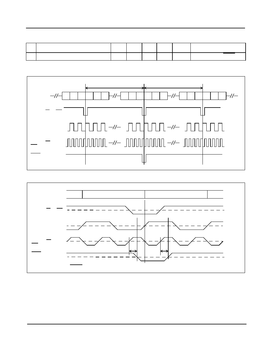
MT9072
Data Sheet
252
Zarlink Semiconductor Inc.
Figure 43 - Receive Multiframe Functional Timing
Figure 44 - Receive Multiframe Timing
AC Electrical Characteristics - Receive MultiframeTiming with TX8KEn Reset
Characteristics
Sym.
Min.
Typ.
Max.
Units
Test Conditions
1
Receive Multiframe Output Delay
t
MOD
55
ns
150 pF load on RxMF
Frame 0
Frame 12 or 24
Bit
1
Bit
0
Bit
7
Bit
6
Bit
5
Bit
2
Bit
1
Bit
0
Bit
7
Bit
6
Bit
5
Bit
2
Bit
1
Bit
0
Bit
7
Bit
6
Bit
5
Bit
2
FPi
(ST-BUS F0i or F16i)
CKi
(ST-BUS C4i or
C16i)
RxMF
(Output)
ST-BUS
Bit Cells
2 Mb/s or 8 Mb/s
CKi
(ST-BUS C2i)
Bit 7
Bit 0
V
T
V
T
V
T
t
MOD
t
MOD
FPi
(ST-BUS F0i or F16i)
CKi
(ST-BUS C4i or
C16i)
RxMF
(Output)
ST-BUS
Bit Cells
2 Mb/s or 8 Mb/s
CKi
(ST-BUS C2i)
V
T
Note: Tx8KEN is 0 RXMF shows the receive T1 multiframe

MT9072
Data Sheet
253
Zarlink Semiconductor Inc.
Figure 45 - Receive Multiframe Timing with TX8KEn Set Functional Timing Diagram
Figure 46 - Receive Multiframe Timing with TX8KEn Set Timing Diagram
AC Electrical Characteristics - Receive MultiframeTiming with TX8KEn Set
Characteristics
Sym.
Min.
Typ.
Max.
Units
Test Conditions
1
RXMF Output Delay
t
TFOD
20
ns
150 pF
AC Electrical Characteristics - Transmit Data Link Timing
Characteristics
Sym.
Min.
Typ.
Max.
Units
Test Conditions
1
Clock Delay
t
CD
100
ns
150 pF load on TxDLC
2
Enable Delay
t
ED
100
ns
150 pF load on TxDLC
3
Data Setup
t
DS
50
ns
150 pF load on TxDLC
4
Data Hold
t
DH
50
ns
150 pF load on TxDLC
RxMF
TPOS/TNEG
Channel 23
Bit 7
Sbit
Channel 0
Bit 1
Channel 0
Bit 2
TXCL
(Tx8KEN= 1)
TPOS/TNEG
t
SOD
(Output)
t
TFOD
t
TFOD
V
TT
V
TT
V
TT
t
SOD
RXMF
(Input)
TXCL
(Output)

MT9072
Data Sheet
254
Zarlink Semiconductor Inc.
Figure 47 - Transmit Data Link Pin Timing
Figure 48 - Receive Data Link Functional Diagram
AC Electrical Characteristics - Transmit Data Link Timing
Characteristics
Sym.
Min.
Typ.
Max.
Units
Test Conditions
1
Clock Delay
t
CD
100
ns
150 pF load on RxDLC
2
Enable Delay
t
ED
100
ns
150 pF load on RxDLC
3
Data Delay Read
t
DDR
100
ns
150 pF load on RxDL
4
Data Hold Read
t
DHR
50
ns
150 pF load on RxDL
MT9072
Inputs Data
t
DH
t
DS
1.5 Mb/s
Bit Cells
TXCL
1.5 Mhz Clock
TxDL
(Input)
V
T
Note 1 - TxDLC output applies for every second frame (FPi) pulse (250 us) only
Note 2 - Clock output provided by setting control bit DLCK=1 (register address Y06)
Note 3 - Enable output provided by clearing control bit DLCK=0 (register address Y06)
Note 4- TXCL is an input 1.5 Mhz clock for the PCM24 interface
Note 5- The TXDLC clock is provided one frame before it is used in ESF Mode in Frames 2 4
TxDLC - Note 3
(Output)
V
T
V
T
TxDLC - Note 2
(Output)
tCD
tED
VT
tCD
RXBF
RxDLC
RxDL

MT9072
Data Sheet
255
Zarlink Semiconductor Inc.
Figure 49 - Receive DataLink Timing Diagram
Figure 50 - Receive Basic Frame Pulse Pin Timing
AC Electrical Characteristics - Receive Basic Frame Pulse Pin Timing
Characteristics
Sym.
Min.
Typ.
Max.
Units
Test Conditions
1
Basic Frame Output Delay
t
BD
100
ns
150 pF load on RxBF
AC Electrical Characteristics - PCM24 Transmit Timing
Characteristics
Sym.
Min.
Typ.
Max.
Units
Test Conditions
1
Transmit Delay
t
TD
50
ns
150 pF load on TPOS and TNEG
2
Transmit Delay in RZ mode
tr
TD
200
ns
150 pF load on TPOS and TNEG
3
Transmit Invalid in RZ Mode
tr
DI
200
ns
150 pF load on TPOS and TNEG
MT9072
Outputs Data
t
CD
V
T
V
T
RxDLC - Note 2
(Output)
RxDL
(Output)
EXCLi
RXDL
Timeslots
V
T
RxDLC - Note 3
(Output)
Note 1 - RxDLC output applies for every second frame (RxBF) pulse (250 us) only
Note 2 - Clock output provided by setting control bit DLCK=1 (register address Y06)
Note 3 - Enable output provided by clearing control bit DLCK=0 (register address Y06)
S bit
Timeslot 23 Bit 8
VT
tDDR
t
ED
V
T
Timeslot23
Bit 8
S
Bit
V
T
t
BD
RxBF
(Output)
EXCLi
RXDL
Bit Cells

MT9072
Data Sheet
256
Zarlink Semiconductor Inc.
Figure 51 - PCM 24 Transmit Timing
MT9072
Outputs Data
MT9072
Outputs Data
PCM 24 Transmit
Bit Cells
1.544 Mb/s
TXCL
(1.544 MHz Clock)
V
T
TPOS or TNEG
(Output)
(NRZ,Clke =0)
TPOS or TNEG
(Output)
(RZ,Clke=0)
V
T
t
TD
V
T
trTD
3.088 MHz Clock
trDI
Note 1 in RZ Mode the data has to sampled on the falling edge of 1.544 MHz clock by an external device.
Note 2 The 3.088 MHz clock is internal and is shown just for reference

MT9072
Data Sheet
257
Zarlink Semiconductor Inc.
Figure 52 - PCM24 Transmit Functional Timing
AC Electrical Characteristics - PCM24 Receive Timing
Characteristics
Sym.
Min.
Typ.
Max.
Units
Test Conditions
1
Receive Setup
t
RS
50
ns
2
Receive Hold
t
RH
50
ns
(0)
(1)
(1)
(1)
TPOS (Output)
(RZ Dual Rail)
TNEG (Output)
(RZ Dual Rail)
PCM24Transmit
Bit Cells (2 Mb/s)
(Sample Data)
TXCL
(1.544 MHz Transmit
Clock Input,clke=0)
TPOS (Output)
(NRZ Dual Rail)
TNEG (Output)
(NRZ Dual Rail)
TPOS (Output)
(NRZ Single Rail)
TNEG (Output)
(NRZ Dual Rail)
TPOS (Output)
(RZ Single Rail)
TNEG (Output)
(RZ Single Rail)
TXCL
(1.544 MHz Transmit
Clock Input,clke=1
Only valid in NRZ
Note: CLKE =1 is only valid in NRZ Mode

MT9072
Data Sheet
258
Zarlink Semiconductor Inc.
Figure 53 - PCM24 Receive Functional Timing
Figure 54 - PCM24 Receive Timing
(0)
(1)
(1)
(1)
RPOS
(Input)
(RZ Dual Rail)
RNEG
(Input)
(RZ Dual Rail)
RPOS
(Input)
(NRZ Dual Rail)
RNEG
(Input)
(NRZ Dual Rail)
RPOS
(Input)
(NRZ Single Rail)
RNEG
(Input)
(NRZ Single Rail)
PCM24 Receive
Bit Cells(Neg Edge)
(Sample Data)
EXCLi
1.5 Meg Clock
CLKE=0
EXCLi
1.5 Meg Clock
CLKE=1
MT9072
Inputs Data
t
RS
t
RH
PCM 24 Receive
Bit Cells
1.544 Mb/s
EXCLi
V
T
RPOS or RNEG
(Input)
(RZ or NRZ Pos
Edge CLKE=0
V
T
EXCLi
V
T
RPOS or RNEG
(Input)
(RZ or NRZ Neg
Edge CLKE=1)
t
RS
t
RH
MT9072
Inputs Data

MT9072
Data Sheet
259
Zarlink Semiconductor Inc.
19.2.1 AC Electrical Characteristics - PCM24 and ST-BUS Frame Format
In both the transmit and receive directions, PCM24 LSB maps to ST-BUS LSB.
Figure 55 - PCM 24 Format
Figure 56 - ST-BUS Format
Typical figures are at 25�C and are for design aid only: not guaranteed and not subject to production testing.
Note 1. High impedance is measured by pulling to the appropriate rail with R
L
, with timing corrected to cancel time taken to discharge
C
L
.
FRAME
15
0
14
15
0
timeslot
0
1
30
31
Most
Significant
Bit (First)
Least
Significant
Bit (Last)
BIT
1
2
3
4
5
6
7
8
FRAME
FRAME
FRAME
FRAME
timeslot
timeslot
timeslot
BIT
BIT
BIT
BIT
BIT
BIT
BIT
2.0 ms
(8/2.048)
�s
125
�s
� � � � � � � �
� � � �
CHANNEL
31 or 127
0
30 or 126
BIT
CHANNEL
CHANNEL
CHANNEL
CHANNEL
31 or 127
0
BIT
BIT
BIT
BIT
BIT
BIT
BIT
� � �
Least
Significant
Bit (Last)
Most
Significant
Bit (First)
125
�s
7
6
5
4
3
2
1
0
(8/2.048 or 8/8.192)
�s
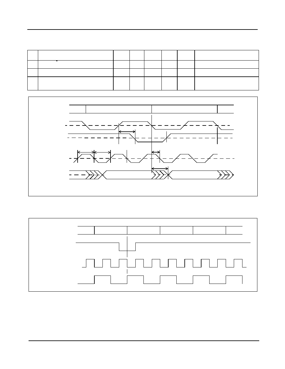
MT9072
Data Sheet
260
Zarlink Semiconductor Inc.
19.3 E1 Mode
Figure 57 - Receive IMA Timing
Figure 58 - Receive IMA Functional Timing Diagram
AC Electrical Characteristics - Receive IMA Timing
Characteristics
Sym.
Min.
Typ.
Max.
Units
Test Conditions
1
RXDLC Clock Width High or Low
t
E4W
25
100
ns
2
Receive Basic Frame Pulse Delay
t
FD
50
ns
4
RXDLC Clock Delay
t
CD
50
125
ns
150 pF load on CSTo and
DSTo
MT9072
Outputs Data
MT9072
Outputs Data
Timeslot 0
Bit 7
Timeslot 31
Bit 0
V
T
t
SOD
V
T
PCM30
Receive
Timeslots
DSTo
(Outputs)
t
CD
V
T
t
E4
H
W
t
E4
L
W
Rxdlc
Output
V
T
EXcli
Input
RXBF
Output
TFD
Note that the Transmit IMA mode uses Fpi Cki and DSTi and timing is indentical to the 2 Mb/s ST-BUS (See Figure 33)
Timeslot 31
Bit 0
Timeslot 0
Bit 7
Timeslot 0
Bit 6
Timeslot 0
Bit 5
RXDLC
RXBF
E2i
ST-BUS
Bit Cells
2 Mb/s
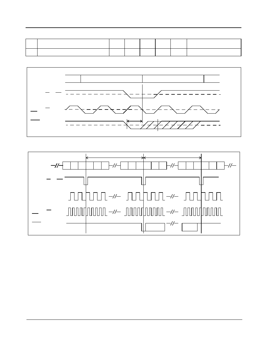
MT9072
Data Sheet
261
Zarlink Semiconductor Inc.
Figure 59 - Transmit Multiframe (CRC-4 or CAS) Timing
Figure 60 - Transmit Multiframe (CRC-4 or CAS) Functional Timing
AC Electrical Characteristics - Transmit Multiframe (CRC-4 or CAS) Timing
Characteristics
Sym.
Min.
Typ.
Max.
Units
Test Conditions
1
Transmit Multiframe Setup
t
MS
50
ns
Frame N
Bit 7 Timeslot 0
Frame 0
V
T
V
T
t
MS
V
T
FPi
(ST-BUS F0i or F16i)
CKi
(ST-BUS C4i or
C16i)
ST-BUS
Bit Cells
2 Mb/s or 8 Mb/s
TxMF
(Input)
Frame 0
Frame N
Bit
1
Bit
0
Bit
7
Bit
6
Bit
5
Bit
2
Bit
1
Bit
0
Bit
7
Bit
6
Bit
5
Bit
2
Bit
1
Bit
0
Bit
7
Bit
6
Bit
5
Bit
2
FPi
(ST-BUS F0i or F16i)
CKi
(ST-BUS C4i or
C16i)
ST-BUS
Bit Cells
2 Mb/s or 8 Mb/s
TxMF
(Input)
Internal
(ST-BUS C2)
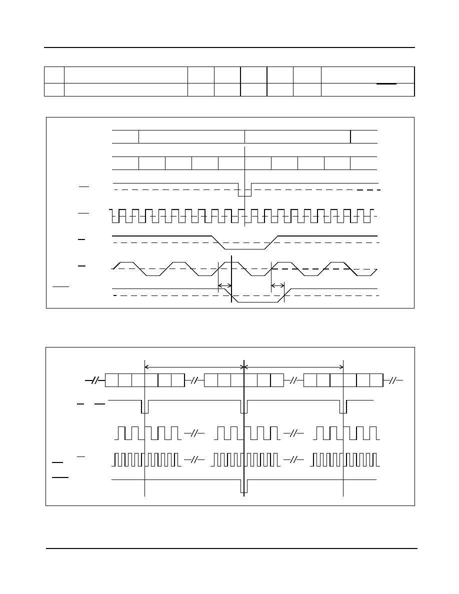
MT9072
Data Sheet
262
Zarlink Semiconductor Inc.
Figure 61 - Receive Multiframe (CRC-4 or CAS) Timing
Figure 62 - Receive Multiframe (CRC-4 or CAS) Functional Timing
AC Electrical Characteristics - Receive Multiframe (CRC-4 or CAS) Timing
Characteristics
Sym.
Min.
Typ.
Max.
Units
Test Conditions
1
Receive Multiframe Output Delay
r
MOD
55
ns
150 pF load on RxMF
Bit 7
Bit 0
Bit 7
Bit 0
V
T
V
T
V
T
r
MOD
r
MOD
FPi
(ST-BUS F0i)
2 Mb/s
CKi
(ST-BUS C4i)
2 Mb/s
RxMF
(Output)
ST-BUS
Bit Cells
2 Mb/s
ST-BUS
Bit Cells
8 Mb/s
CKi
(ST-BUS C16i)
8 Mb/s
V
T
V
T
FPi
(ST-BUS F16i)
8 Mb/s
Frame 0
Frame 15
Bit
1
Bit
0
Bit
7
Bit
6
Bit
5
Bit
2
Bit
1
Bit
0
Bit
7
Bit
6
Bit
5
Bit
2
Bit
1
Bit
0
Bit
7
Bit
6
Bit
5
Bit
2
FPi
(ST-BUS F0i or F16i)
CKi
(ST-BUS C4i or
C16i)
RxMF
(Output)
ST-BUS
Bit Cells
2 Mb/s or 8 Mb/s
Internal
(ST-BUS C2 or C8)

MT9072
Data Sheet
263
Zarlink Semiconductor Inc.
Figure 63 - Receive Multiframe Timing with TX8KEn Set
Figure 64 - Receive Multiframe Timing with TX8KEn Set
AC Electrical Characteristics - Receive MultiframeTiming with TX8KEn Set
Characteristics
Sym.
Min.
Typ.
Max.
Units
Test Conditions
1
RXMF Output Delay
t
TFOD
20
ns
150 pF
TPOS/TNEG
t
SOD
(Output)
t
TFOD
t
TFOD
V
TT
V
TT
V
TT
t
SOD
RXMF
(Output)
T2o
(Output)
RxMF
TPOS/TNEG
Channel 31
Bit 8
Channel 0
Channel 0
Bit 2
Channel 0
Bit3
T2O
(Tx8KEN= 1)
Bit 1

MT9072
Data Sheet
264
Zarlink Semiconductor Inc.
Figure 65 - Transmit Data Link Pin Timing
AC Electrical Characteristics - Transmit Data Link Pin Timing
Characteristics
Sym.
Min.
Typ.
Max.
Units
Test Conditions
1
Clock Delay
t
CD
55
ns
150 pF load on TxDLC
2
Enable Delay
t
ED
55
ns
150 pF load on TxDLC
3
Data Setup
t
DS
100
ns
4
Data Hold
t
DH
50
ns
MT9072
Inputs Data
t
DH
t
DS
ST-BUS
Bit Cells
2 Mb/s
CKi
(ST-BUS C4i)
2 Mb/s
V
T
TxDL
(Input)
V
T
Note 1 - TxDLC output applies for every second frame (FPi) pulse (250 us) only
Note 2 - Clock output provided by setting control bit DLCK=1 (register address Y08)
Note 3 - Enable output provided by clearing control bit DLCK=0 (register address Y08)
t
ED
t
ED
TxDLC - Note 3
(Output)
V
T
V
T
t
CD
t
CD
TxDLC - Note 2
(Output)
ST-BUS
Bit Cells
8 Mb/s
CKi
(ST-BUS C16i)
8 Mb/s
V
T

MT9072
Data Sheet
265
Zarlink Semiconductor Inc.
Figure 66 - Transmit Data Link Pin Functional Timing
Bit
76543210
Example A - enable output
Example B - 12 kbit/s clock output
Sa4 to Sa8 clocked in by MT9072
Sa4, Sa7 and Sa8 clocked in by MT9072
Timeslot 0
Bit
1
Bit
0
Bit
7
Bit
6
Bit
5
Bit
2
Bit
4
Bit
3
Bit
7
Bit
6
Bit
5
Bit
4
Bit
1
Bit
0
Bit
7
Bit
6
Bit
5
Bit
2
Bit
4
Bit
3
Timeslot 31
Timeslot 1
Bit
Sa7
Bit
Sa8
Bit
Sa6
Bit
Sa4
Bit
Sa5
Bit
7
Bit
6
Bit
5
Bit
7
Bit
6
Bit
5
Bit
4
Bit
1
Bit
0
Bit
7
Bit
6
Bit
5
Bit
2
Bit
4
Bit
3
FPi
(ST-BUS F0i)
CKi
(ST-BUS C4i)
TxDLC - Note 3
(Output)
TxDL
(Input)
(2Mb/s)
TxDLC - Note 2
(Output)
ST-BUS
Bit Cells
2 Mb/s
Internal
(ST-BUS C2)
ST-BUS
Bit Cells
8 Mb/s
Bit
76543210
Bit
76543210
TS2
TS4
TS1
TS0
TS127
TS126
TS125
TS124
TS3
TS5
Bit
76543210
Bit
76543210
Bit
76543210
Bit
76543210
Bit
76543210
Bit
76543210
Bit
76543210
CKi
(ST-BUS C16i)
Example A - 20 kbit/s clock output
Sa4 to Sa8 clocked in by MT9072
TxDLC - Note 2
(Output)
Note 1 - TxDLC output applies for every second frame (FPi) pulse (250 us) only
Note 2 - Clock output provided by setting control bit DLCK=1 (register address Y08)
Note 3 - Enable output provided by clearing control bit DLCK=0 (register address Y08)
Example B - enable output
Sa4, Sa7 and Sa8 clocked in by MT9072
TxDLC - Note 3
(Output)
FPi
(ST-BUS F16i)

MT9072
Data Sheet
266
Zarlink Semiconductor Inc.
Figure 67 - Receive Basic Frame and E4o Timing
AC Electrical Characteristics - Receive Basic Frame and E4o Timing
Characteristics
Sym.
Min.
Typ.
Max.
Units
Test Conditions
1
Basic Frame Output Delay
t
BD
30
115
ns
150 pF load on RxBF
2
Clock Delay
t
CD
55
ns
150 pF load on RxDLC
3
E4o Clock High Width
t
E4HW
50
200
ns
150 pF load on RxDLC
3
E4o Clock Low Width
t
E4LW
25
75
ns
150 pF load on RxDLC
V
T
Timeslot 31
Bit 8
Timeslot 0
Bit 1
V
T
RxBF
(Output)
E2i
Input
RXDL
PCM 30
Bit Cells
E4o - Note 1
(RxDLC Pin)
Output
t
CD
t
CD
Note 1 - The E4o signal is output at the RxDLC Pin when the E4CK control bit (address Y08) is set to one.
Note 2 - The PCM Timeslots are referred to RXDL Output which is delayed 4 bits from the RPOS/RNEG input.
Note3- The E4o Clock(RXDLC Output) is not a 50% duty cycle clock, it will be low for 25 % and high for 75% of the
4.096 MHz clock
V
T
t
E4
H
W
t
E4
L
W
t
BD
t
BD

MT9072
Data Sheet
267
Zarlink Semiconductor Inc.
Figure 68 - Receive Data Link Timing
AC Electrical Characteristics - Receive Data Link Timing
Characteristics
Sym.
Min.
Typ.
Max.
Units
Test Conditions
1
Clock Delay
t
CD
55
ns
150 pF load on RxDLC
2
Enable Delay
t
ED
55
ns
150 pF load on RxDLC
3
Data Delay Read
t
DDR
125
ns
150 pF load on RxDL
MT9072
Outputs Data
t
CD
V
T
V
T
V
T
t
DDR
t
CD
RxDLC - Note 2
(Output)
RxDL
(Output)
E2i
RXDL
Bit Cells
V
T
t
ED
t
ED
RxDLC - Note 3
(Output)
Note 1 - RxDLC output applies for every second frame (RxBF) pulse (250us) only
Note 2 - Clock output provided by setting control bit DLCK=1 (register address Y08)
Note 3 - Enable output provided by clearing control bit DLCK=0 (register address Y08)
Note 4 - The PCM 30 Timeslots are with respect to RXDL Output

MT9072
Data Sheet
268
Zarlink Semiconductor Inc.
Figure 69 - Receive Data Link Pin Functional Timing
RxBF
(Output)
Timeslot 0
Bit
1
Bit
0
Bit
7
Bit
6
Bit
5
Bit
2
Bit
4
Bit
3
Bit
7
Bit
6
Bit
5
Bit
4
Bit
1
Bit
0
Bit
7
Bit
6
Bit
5
Bit
2
Bit
4
Bit
3
Timeslot 31
Timeslot 1
Bit
Sa7
Bit
Sa8
Bit
Sa6
Bit
Sa4
Bit
Sa5
Bit
7
Bit
6
Bit
5
Bit
7
Bit
6
Bit
5
Bit
4
Bit
1
Bit
0
Bit
7
Bit
6
Bit
5
Bit
2
Bit
4
Bit
3
Example A - 20 kbit/s clock output
Example B - 12 kbit/s clock output
Sa4 to Sa8 clocked in by External Device
Sa4, Sa7 and Sa8 clocked in by External Device
RxDLC - Note 2
(Output)
RxDLC - Note 2
(Output)
RxDL
(Output)
E2i
RXDL
PCM 30
Bit Cells
Example B - enable output
Sa4, Sa7 and Sa8 clocked in by External Device
RxDLC - Note 3
(Output)
RxDLC - Note 3
(Output)
Example A - enable output
Sa4 to Sa8 clocked in by External Device
Note 1 - RxDLC output applies for every second frame (RxBF) pulse (250 us) only
Note 2 - Clock output provided by setting control bit DLCK=1 (register address Y08)
Note 3 - Enable output provided by clearing control bit DLCK=0 (register address Y08)
Note 4 - PCM Timeslot is with reference to RXDL Output. It is delayed 4 bits from RPOS/RNEG
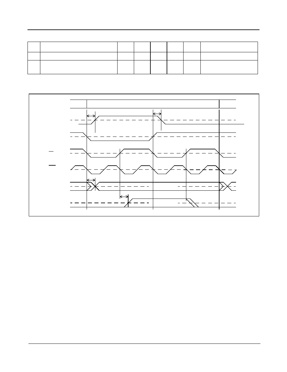
MT9072
Data Sheet
269
Zarlink Semiconductor Inc.
Figure 70 - PCM 30 Transmit Timing
AC Electrical Characteristics - PCM30 Transmit Timing
Characteristics
Sym.
Min.
Typ.
Max.
Units
Test Conditions
1
Transmit Output Clock Delay
t
CD
55
ns
150 pF load on T2o
2
Transmit Output Delay
t
TOD
55
ns
150 pF load on TPOS
and TNEG
MT9072
Outputs Data
MT9072
Outputs Data
V
T
CKi
(ST-BUS C16i)
PCM 30 Transmit
Bit Cells
2 Mb/s
CKi
(ST-BUS C4i)
V
T
TPOS or TNEG
(Output)
(NRZ)
TPOS or TNEG
(Output)
(RZ)
V
T
t
TOD
t
TOD
V
T
V
T
T2o
(Output)
T2OP=0
V
T
T2o
(Output)
T2OP=1
t
CD
t
CD
Note that the times specified apply to non-loopback modes

MT9072
Data Sheet
270
Zarlink Semiconductor Inc.
Figure 71 - PCM30 Transmit Functional Timing
(0)
(1)
(1)
(1)
CKi
(ST-BUS C4i)
TPOS (Output)
(RZ Dual Rail)
TNEG (Output)
(RZ Dual Rail)
TPOS
(Output)
(NRZ Dual Rail)
TNEG
(Output)
(NRZ Dual Rail)
TPOS
(Output)
(NRZ Single Rail)
TNEG
(Output)
(NRZ Single Rail)
PCM30 Transmit
Bit Cells (2 Mb/s)
(Sample Data)
T2o
(Output)
T2OP=0
CKi
(ST-BUS C16i)
T2o
(Output)
T2OP=1
Note: T2o is only applicable in the NRZ mode

MT9072
Data Sheet
271
Zarlink Semiconductor Inc.
Figure 72 - PCM 30 Receive Timing
Figure 73 - PCM30 Receive Functional Timing
AC Electrical Characteristics - PCM30 Receive Timing
Characteristics
Sym.
Min.
Typ.
Max.
Units
Test Conditions
1
Receive Setup
t
RS
50
ns
2
Receive Hold
t
RH
50
ns
MT9072
Inputs Data
t
RS
t
RH
PCM 30 Receive
Bit Cells
2 Mb/s
E2i
V
T
RPOS or RNEG
(Input)
(RZ or NRZ)
V
T
(0)
(1)
(1)
(1)
RPOS
(Input)
(RZ Dual Rail)
RNEG
(Input)
(RZ Dual Rail)
RPOS
(Input)
(NRZ Dual Rail)
RNEG
(Input)
(NRZ Dual Rail)
RPOS
(Input)
(NRZ Single Rail)
RNEG
(Input)
(NRZ Single Rail)
PCM30 Receive
Bit Cells(Neg Edge)
(Sample Data)
E2i
2 Meg Clock
CLKE=0
E2i
2 Meg Clock
CLKE=1
ClKE selection is noly applicable for NRZ mode

MT9072
Data Sheet
272
Zarlink Semiconductor Inc.
19.4 AC Electrical Characteristics - PCM30 and ST-BUS Frame Format
In both the transmit and receive directions, PCM30 LSB maps to ST-BUS LSB.
Figure 74 - PCM 30 Format
Figure 75 - ST-BUS Format
20.0 Applicable Specifications
Standard
Title
T1.102-1993
Digital Heirarchy_Electrical Interfaces
T1.231-1993
Layer 1 In-Service Digital Transmission Performance Monitoring
T1.403-1995
Network to Customer Installation Metallic Interfaces
T1.408-1990
ISDN Primary Rate- Customer Installation Metallic Interfaces
TR 62411-1990
Accunet T1.5 Service Description and Interface Specification
TA-TSY-000278 Issue1, 1985
Digital Data Systems(DDS)- T1 Digital Multiplexor(T1DM) Requirements
G.711
Pulse Code Modulation(PCM) of Voice Frequencies
Table 204 - Applicable Telecommunications Specifications
FRAME
15
0
14
15
0
TIMESLOT
0
1
30
31
Most
Significant
Bit (First)
Least
Significant
Bit (Last)
BIT
1
2
3
4
5
6
7
8
FRAME
FRAME
FRAME
FRAME
TIMESLOT
TIMESLOT
TIMESLOT
BIT
BIT
BIT
BIT
BIT
BIT
BIT
2.0 ms
(8/2.048)
�s
125
�s
� � � � � � � �
� � � �
CHANNEL
31 or 127
0
30 or 126
BIT
CHANNEL
CHANNEL
CHANNEL
CHANNEL
31 or 127
0
BIT
BIT
BIT
BIT
BIT
BIT
BIT
� � �
Least
Significant
Bit (Last)
Most
Significant
Bit (First)
125
�s
7
6
5
4
3
2
1
0
(8/2.048 or 8/8.192)
�s


c Zarlink Semiconductor 2002 All rights reserved.
APPRD.
ISSUE
DATE
ACN
Package Code
Previous package codes:

www.zarlink.com
Information relating to products and services furnished herein by Zarlink Semiconductor Inc. or its subsidiaries (collectively "Zarlink") is believed to be reliable.
However, Zarlink assumes no liability for errors that may appear in this publication, or for liability otherwise arising from the application or use of any such
information, product or service or for any infringement of patents or other intellectual property rights owned by third parties which may result from such application or
use. Neither the supply of such information or purchase of product or service conveys any license, either express or implied, under patents or other intellectual
property rights owned by Zarlink or licensed from third parties by Zarlink, whatsoever. Purchasers of products are also hereby notified that the use of product in
certain ways or in combination with Zarlink, or non-Zarlink furnished goods or services may infringe patents or other intellectual property rights owned by Zarlink.
This publication is issued to provide information only and (unless agreed by Zarlink in writing) may not be used, applied or reproduced for any purpose nor form part
of any order or contract nor to be regarded as a representation relating to the products or services concerned. The products, their specifications, services and other
information appearing in this publication are subject to change by Zarlink without notice. No warranty or guarantee express or implied is made regarding the
capability, performance or suitability of any product or service. Information concerning possible methods of use is provided as a guide only and does not constitute
any guarantee that such methods of use will be satisfactory in a specific piece of equipment. It is the user's responsibility to fully determine the performance and
suitability of any equipment using such information and to ensure that any publication or data used is up to date and has not been superseded. Manufacturing does
not necessarily include testing of all functions or parameters. These products are not suitable for use in any medical products whose failure to perform may result in
significant injury or death to the user. All products and materials are sold and services provided subject to Zarlink's conditions of sale which are available on request.
Purchase of Zarlink's I
2
C components conveys a licence under the Philips I
2
C Patent rights to use these components in and I
2
C System, provided that the system
conforms to the I
2
C Standard Specification as defined by Philips.
Zarlink, ZL and the Zarlink Semiconductor logo are trademarks of Zarlink Semiconductor Inc.
Copyright Zarlink Semiconductor Inc. All Rights Reserved.
TECHNICAL DOCUMENTATION - NOT FOR RESALE
For more information about all Zarlink products
visit our Web Site at