Document Outline
- Features
- Applications
- Description
- Figure 1 - Functional Block Diagram
- Changes Summary
- Figure 2 - 160-Pin MQFP Pin Connections
- Figure 3 - 160 Ball PBGA Pin Connections
- Figure 4 - 144 Ball LBGA Pin Connections
- Pin Description�
- 1.0 Device Overview
- Table 1 - Stream Usage under Various Operation Modes
- Table 2 - Output High Impedance Control
- Table 3 - Address Map for Registers (A13 = 0)�
- 2.0 Functional Description
- 2.1 Data and Connection Memory
- 2.2 Connection and Message Modes
- 2.3 Clock Timing Requirements
- 3.0 Switching Configurations
- 3.1 Serial Input Frame Alignment Evaluation
- 3.2 Input Frame Offset Selection
- 3.3 Output Advance Offset Selection
- Table 4 - Address Map for Memory Locations (A13 = 1)
- 3.4 Memory Block Programming
- 3.5 Bit Error Rate Monitoring
- 4.0 Delay Through the MT90826
- 4.1 Variable Delay Mode (TM1=0, TM0=0)
- 4.2 Constant Delay Mode (TM1=1, TM0=0)
- 5.0 Microprocessor Interface
- Table 5 - Control Register Bits�
- Table 6 - Serial Data Rate Selections and External Clock Rates
- Table 7 - Frame Alignment (FAR) Register Bits
- Figure 5 - Example for Frame Alignment Measurement
- Table 8 - Frame Delay Offset Register (DOS) Bits�
- Table 9 - Frame delay Bits (FD9, FD2-0) and Input Offset Bits (IFn3-0)
- Figure 6 - Examples for Input Offset Delay Timing
- Table 10 - Frame Output Offset (FOR) Register Bits
- Table 11 - Output Offset Bits (FD9, FD2-0)
- Figure 7 - Examples for Frame Output Offset Timing
- Table 12 - Bit Error Input Selection (BISR) Register Bits
- Table 13 - Bit Error Count (BECR) Register Bits
- 6.0 Memory Mapping
- 7.0 Connection Memory Control
- 8.0 DTA Data Transfer Acknowledgment Pin
- 9.0 Initialization of the MT90826
- 10.0 JTAG Support
- 10.1 Test Access Port (TAP)
- 10.2 Instruction Register
- Test Data Register
- Table 14 - Connection Memory Bits
- Table 15 - SAB and CAB Bits Programming for Various Interface Mode
- Absolute Maximum Ratings*
- Recommended Operating Conditions - Voltages are with respect to ground (Vss) unless otherwise sta...
- DC Electrical Characteristics - Voltages are with respect to ground (Vss) unless otherwise stated.
- AC Electrical Characteristics - Timing Parameter Measurement Voltage Levels
- AC Electrical Characteristics - Frame Pulse and CLK
- AC Electrical Characteristics - Serial Streams for ST-BUS�
- Figure 8 - ST-BUS Timing for Stream rate of 16.384�Mbps
- Figure 9 - ST-BUS Timing for Stream rate of 8.192�Mbps when CLK = 16.384�MHz
- Figure 10 - ST-BUS Timing for Stream rate of 4.096�Mbps when CLK = 16.384�MHz
- Figure 11 - ST-BUS Timing for Stream rate of 4.096�Mbps when CLK = 8.192�MHz
- Figure 12 - ST-BUS Timing for Stream rate of 2.048�Mbps when CLK = 16.384�MHz
- Figure 13 - -BUS Timing for Stream rate of 2.048�Mbps when CLK = 8.192�MHz
- Figure 14 - Serial Output and External Control
- Figure 15 - Output Driver Enable (ODE)
- AC Electrical Characteristics - Motorola Non-Multiplexed Bus Mode
- Figure 16 - Motorola Non-Multiplexed Bus Timing
1
Zarlink Semiconductor Inc.
Zarlink, ZL and the Zarlink Semiconductor logo are trademarks of Zarlink Semiconductor Inc.
Copyright 2003-2005, Zarlink Semiconductor Inc. All Rights Reserved.
Features
� 4,096
� 4,096 channel non-blocking switching at
8.192 or 16.384 Mbps
� Per-channel variable or constant throughput
delay
� Accepts 32 ST-BUS streams of 2.048 Mbps,
4.096 Mbps, 8.192 Mbps or 16.384 Mbps
� Split Rate mode provides a rate conversion option
to convert data from one rate to another rate
� Automatic frame offset delay measurement for
ST-BUS input streams
� Per-stream input delay programming
� Per-stream output advancement programming
� Per-channel high impedance output control
� Bit Error Monitoring on selected ST-BUS input
and output channels.
� Per-channel message mode
� Connection memory block programming
� IEEE-1149.1 (JTAG) Test Port
� 3.3 V local I/O with 5 V tolerant inputs and TTL
compatible outputs
Applications
� Medium switching platforms
� CTI application
� Voice/data multiplexer
� Digital cross connects
� WAN access system
� Wireless base stations
August 2005
Ordering Information
MT90826AL
160 Pin MQFP
Trays
MT90826AG
160 Ball PBGA
Trays
MT90826AV
144 Ball LBGA
Trays
MT90826AL1
160 Pin MQFP*
Trays
*Pb Free Matte Tin
-40
�C to +85�C
MT90826
Quad Digital Switch
Data Sheet
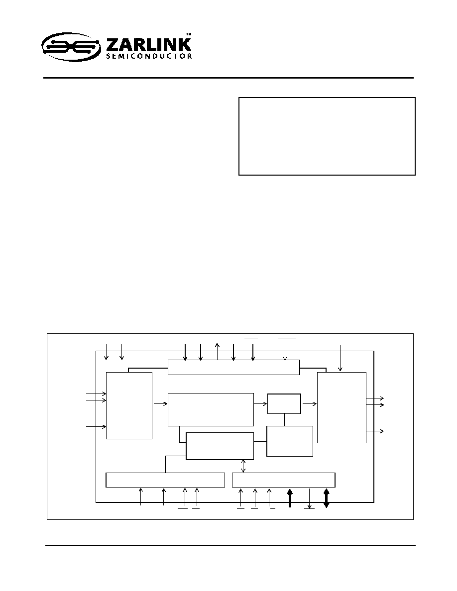
Figure 1 - Functional Block Diagram
Test Port
STo0
STo1
�
�
�
STo31
STi0/FEi0
STi1/FEi1
�
�
�
STi31/FEi31
Parallel
to
Serial
Converter
Output
MUX
Microprocessor Interface
Timing Unit
Internal
Registers
F0i
DS
CS
R/W
A13-A0 DTA
D15-D0
ODE
V
SS
Connection
Memory
CLK
V
DD
TDI TDO
RESET
TCK
TRST
Serial
to
Parallel
Converter
TMS
Multiple Buffer
Data Memory
PLLV
SS
PLLV
DD

MT90826
Data Sheet
2
Zarlink Semiconductor Inc.
Description
The MT90826 Quad Digital Switch has a non-blocking switch capacity of 4,096 x 4,096 channels at a serial bit rate
of 8.192 Mbps or 16.384 Mbps, 2,048 x 2,048 channels at 4.096 Mbps and 1024 x 1024 channels at 2.048 Mbps.
The device has many features that are programmable on a per stream or per channel basis, including message
mode, input offset delay and high impedance output control.
The per stream input and output delay control is particularly useful for managing large multi-chip switches with a
distributed backplane.
Operating in Split Rate mode allows rate conversion for switching between two groups of bit rate streams.

MT90826
Data Sheet
Table of Contents
3
Zarlink Semiconductor Inc.
1.0 Device Overview . . . . . . . . . . . . . . . . . . . . . . . . . . . . . . . . . . . . . . . . . . . . . . . . . . . . . . . . . . . . . . . . . . . . . . 12
2.0 Functional Description . . . . . . . . . . . . . . . . . . . . . . . . . . . . . . . . . . . . . . . . . . . . . . . . . . . . . . . . . . . . . . . . . 14
2.1 Data and Connection Memory. . . . . . . . . . . . . . . . . . . . . . . . . . . . . . . . . . . . . . . . . . . . . . . . . . . . . . . . . . 14
2.2 Connection and Message Modes . . . . . . . . . . . . . . . . . . . . . . . . . . . . . . . . . . . . . . . . . . . . . . . . . . . . . . . 14
2.3 Clock Timing Requirements . . . . . . . . . . . . . . . . . . . . . . . . . . . . . . . . . . . . . . . . . . . . . . . . . . . . . . . . . . . 15
3.0 Switching Configurations . . . . . . . . . . . . . . . . . . . . . . . . . . . . . . . . . . . . . . . . . . . . . . . . . . . . . . . . . . . . . . . 15
3.1 Serial Input Frame Alignment Evaluation . . . . . . . . . . . . . . . . . . . . . . . . . . . . . . . . . . . . . . . . . . . . . . . . . 16
3.2 Input Frame Offset Selection. . . . . . . . . . . . . . . . . . . . . . . . . . . . . . . . . . . . . . . . . . . . . . . . . . . . . . . . . . . 16
3.3 Output Advance Offset Selection . . . . . . . . . . . . . . . . . . . . . . . . . . . . . . . . . . . . . . . . . . . . . . . . . . . . . . . 16
3.4 Memory Block Programming . . . . . . . . . . . . . . . . . . . . . . . . . . . . . . . . . . . . . . . . . . . . . . . . . . . . . . . . . . . 17
3.5 Bit Error Rate Monitoring . . . . . . . . . . . . . . . . . . . . . . . . . . . . . . . . . . . . . . . . . . . . . . . . . . . . . . . . . . . . . . 17
4.0 Delay Through the MT90826 . . . . . . . . . . . . . . . . . . . . . . . . . . . . . . . . . . . . . . . . . . . . . . . . . . . . . . . . . . . . . 18
4.1 Variable Delay Mode (TM1=0, TM0=0) . . . . . . . . . . . . . . . . . . . . . . . . . . . . . . . . . . . . . . . . . . . . . . . . . . . 18
4.2 Constant Delay Mode (TM1=1, TM0=0) . . . . . . . . . . . . . . . . . . . . . . . . . . . . . . . . . . . . . . . . . . . . . . . . . . 18
5.0 Microprocessor Interface . . . . . . . . . . . . . . . . . . . . . . . . . . . . . . . . . . . . . . . . . . . . . . . . . . . . . . . . . . . . . . . 18
6.0 Memory Mapping . . . . . . . . . . . . . . . . . . . . . . . . . . . . . . . . . . . . . . . . . . . . . . . . . . . . . . . . . . . . . . . . . . . . . . 29
7.0 Connection Memory Control. . . . . . . . . . . . . . . . . . . . . . . . . . . . . . . . . . . . . . . . . . . . . . . . . . . . . . . . . . . . . 29
8.0 DTA Data Transfer Acknowledgment Pin . . . . . . . . . . . . . . . . . . . . . . . . . . . . . . . . . . . . . . . . . . . . . . . . . . 29
9.0 Initialization of the MT90826 . . . . . . . . . . . . . . . . . . . . . . . . . . . . . . . . . . . . . . . . . . . . . . . . . . . . . . . . . . . . . 30
10.0 JTAG Support. . . . . . . . . . . . . . . . . . . . . . . . . . . . . . . . . . . . . . . . . . . . . . . . . . . . . . . . . . . . . . . . . . . . . . . . 30
10.1 Test Access Port (TAP) . . . . . . . . . . . . . . . . . . . . . . . . . . . . . . . . . . . . . . . . . . . . . . . . . . . . . . . . . . . . . . 30
10.2 Instruction Register . . . . . . . . . . . . . . . . . . . . . . . . . . . . . . . . . . . . . . . . . . . . . . . . . . . . . . . . . . . . . . . . . 31

MT90826
Data Sheet
List of Figures
4
Zarlink Semiconductor Inc.
Figure 1 - Functional Block Diagram . . . . . . . . . . . . . . . . . . . . . . . . . . . . . . . . . . . . . . . . . . . . . . . . . . . . . . . . . . . . 1
Figure 2 - 160-Pin MQFP Pin Connections . . . . . . . . . . . . . . . . . . . . . . . . . . . . . . . . . . . . . . . . . . . . . . . . . . . . . . . 7
Figure 3 - 160 Ball PBGA Pin Connections . . . . . . . . . . . . . . . . . . . . . . . . . . . . . . . . . . . . . . . . . . . . . . . . . . . . . . . 8
Figure 4 - 144 Ball LBGA Pin Connections . . . . . . . . . . . . . . . . . . . . . . . . . . . . . . . . . . . . . . . . . . . . . . . . . . . . . . . 9
Figure 5 - Example for Frame Alignment Measurement . . . . . . . . . . . . . . . . . . . . . . . . . . . . . . . . . . . . . . . . . . . . 22
Figure 6 - Examples for Input Offset Delay Timing . . . . . . . . . . . . . . . . . . . . . . . . . . . . . . . . . . . . . . . . . . . . . . . . 26
Figure 7 - Examples for Frame Output Offset Timing . . . . . . . . . . . . . . . . . . . . . . . . . . . . . . . . . . . . . . . . . . . . . . 28
Figure 8 - ST-BUS Timing for Stream rate of 16.384 Mbps . . . . . . . . . . . . . . . . . . . . . . . . . . . . . . . . . . . . . . . . . . 37
Figure 9 - ST-BUS Timing for Stream rate of 8.192 Mbps when CLK = 16.384 MHz . . . . . . . . . . . . . . . . . . . . . . 38
Figure 10 - ST-BUS Timing for Stream rate of 4.096 Mbps when CLK = 16.384 MHz . . . . . . . . . . . . . . . . . . . . . 38
Figure 11 - ST-BUS Timing for Stream rate of 4.096 Mbps when CLK = 8.192 MHz. . . . . . . . . . . . . . . . . . . . . . . 38
Figure 12 - ST-BUS Timing for Stream rate of 2.048 Mbps when CLK = 16.384 MHz . . . . . . . . . . . . . . . . . . . . . 39
Figure 13 - -BUS Timing for Stream rate of 2.048 Mbps when CLK = 8.192 MHz. . . . . . . . . . . . . . . . . . . . . . . . . 39
Figure 14 - Serial Output and External Control . . . . . . . . . . . . . . . . . . . . . . . . . . . . . . . . . . . . . . . . . . . . . . . . . . . 39
Figure 15 - Output Driver Enable (ODE) . . . . . . . . . . . . . . . . . . . . . . . . . . . . . . . . . . . . . . . . . . . . . . . . . . . . . . . . 40
Figure 16 - Motorola Non-Multiplexed Bus Timing. . . . . . . . . . . . . . . . . . . . . . . . . . . . . . . . . . . . . . . . . . . . . . . . . 42

MT90826
Data Sheet
List of Tables
5
Zarlink Semiconductor Inc.
Table 1 - Stream Usage under Various Operation Modes . . . . . . . . . . . . . . . . . . . . . . . . . . . . . . . . . . . . . . . . . . . 13
Table 2 - Output High Impedance Control . . . . . . . . . . . . . . . . . . . . . . . . . . . . . . . . . . . . . . . . . . . . . . . . . . . . . . . 13
Table 3 - Address Map for Registers (A13 = 0) . . . . . . . . . . . . . . . . . . . . . . . . . . . . . . . . . . . . . . . . . . . . . . . . . . . 13
Table 4 - Address Map for Memory Locations (A13 = 1) . . . . . . . . . . . . . . . . . . . . . . . . . . . . . . . . . . . . . . . . . . . . 17
Table 5 - Control Register Bits . . . . . . . . . . . . . . . . . . . . . . . . . . . . . . . . . . . . . . . . . . . . . . . . . . . . . . . . . . . . . . . . 19
Table 6 - Serial Data Rate Selections and External Clock Rates. . . . . . . . . . . . . . . . . . . . . . . . . . . . . . . . . . . . . . 20
Table 7 - Frame Alignment (FAR) Register Bits . . . . . . . . . . . . . . . . . . . . . . . . . . . . . . . . . . . . . . . . . . . . . . . . . . . 21
Table 8 - Frame Delay Offset Register (DOS) Bits. . . . . . . . . . . . . . . . . . . . . . . . . . . . . . . . . . . . . . . . . . . . . . . . . 23
Table 9 - Frame delay Bits (FD9, FD2-0) and Input Offset Bits (IFn3-0) . . . . . . . . . . . . . . . . . . . . . . . . . . . . . . . . 25
Table 10 - Frame Output Offset (FOR) Register Bits . . . . . . . . . . . . . . . . . . . . . . . . . . . . . . . . . . . . . . . . . . . . . . . 27
Table 11 - Output Offset Bits (FD9, FD2-0) . . . . . . . . . . . . . . . . . . . . . . . . . . . . . . . . . . . . . . . . . . . . . . . . . . . . . . 27
Table 12 - Bit Error Input Selection (BISR) Register Bits . . . . . . . . . . . . . . . . . . . . . . . . . . . . . . . . . . . . . . . . . . . . 28
Table 13 - Bit Error Count (BECR) Register Bits . . . . . . . . . . . . . . . . . . . . . . . . . . . . . . . . . . . . . . . . . . . . . . . . . . 28
Table 14 - Connection Memory Bits . . . . . . . . . . . . . . . . . . . . . . . . . . . . . . . . . . . . . . . . . . . . . . . . . . . . . . . . . . . . 34
Table 15 - SAB and CAB Bits Programming for Various Interface Mode . . . . . . . . . . . . . . . . . . . . . . . . . . . . . . . . 34