 | Рлектронный компонент: NJ8821 | Скачать:  PDF PDF  ZIP ZIP |

Obsolescence Notice
This product is obsolete.
This information is available for your
convenience only.
For more information on
Zarlink's obsolete products and
replacement product lists, please visit
http://products.zarlink.com/obsolete_products/

THIS DOCUMENT IS FOR MAINTENANCE
PURPOSES ONLY AND IS NOT
RECOMMENDED FOR NEW DESIGNS
NJ8821
NJ8821
FREQUENCY SYNTHESISER (MICROPROCESSOR INTERFACE)
WITH RESETTABLE COUNTERS
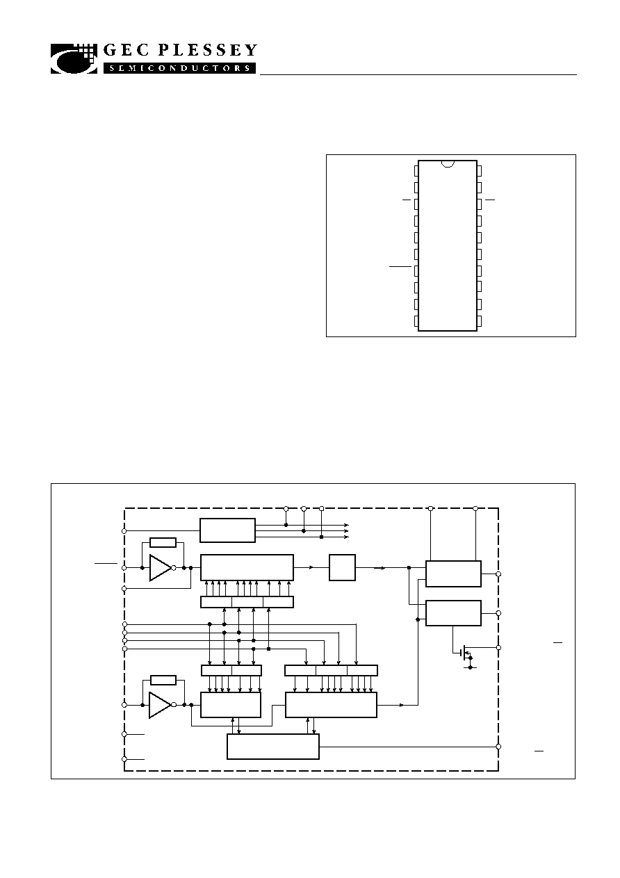
Fig.2 Block diagram
PROGRAM
ENABLE (PE)
OSC IN
OSC OUT
D0
D1
D2
D3
F
IN
V
DD
V
SS
LATCH 1
LATCH 2
LATCH 3
`M' COUNTER
(10 BITS)
CONTROL LOGIC
LATCH 4
LATCH 5
`A' COUNTER
(7 BITS)
FREQUENCY/
PHASE
DETECTOR
V
SS
PDA
PDB
LOCK DETECT (LD)
MODULUS
CONTROL
OUTPUT (MC)
RB CH
15 16 17
f
v
REFERENCE COUNTER
(11BITS)
LATCH 6
LATCH 7
LATCH 8
4
2
SAMPLE/HOLD
PHASE
DETECTOR
f
r
LATCH SELECT
LOGIC
DS0 DS1 DS2
14
7
8
9
10
11
12
4
6
5
TO
INTERNAL
LATCHES
DATA SELECT INPUTS
19 20
1
2
3
18
DATA
INPUTS
ABSOLUTE MAXIMUM RATINGS
Supply voltage, V
DD
2V
SS
Input voltage
Open drain output, pin 3
All other pins
Storage temperature
Storage temperature
20·5V to 7V
7V
V
SS
20·3V to V
DD
10·3V
265
°
C to
1150
°
C
(DG package, NJ8821MA)
255
°
C to 1125
°
C
(DP and MP packages, NJ8821)
ORDERING INFORMATION
NJ8821 BA DP Plastic DIL Package
NJ8821 BA MP Miniature Plastic DIL Package
NJ8821 MA DG Ceramic DIL Package
The NJ8821 is a synthesiser circuit fabricated on the GPS
CMOS process and is capable of achieving high sideband
attenuation and low noise performance. It contains a reference
oscillator, 11-bit programmable reference divider, digital and
sample-and-hold comparators, 10-bit programmable `M' counter,
7-bit programmable `A' counter and the necessary control and
latch circuitry for accepting and latching the input data.
Data is presented as eight 4-bit words under external control
from a suitable microprocessor..
It is intended to be used in conjunction with a two-modulus
prescaler such as the SP8710 series to produce a universal
binary coded synthesiser.
The NJ8821 is available in Plastic DIL (DP) and Miniature
Plastic DIL (MP) packages, both with operating temperature
range of 230
°
C to 170
°
C. The NJ8821MA is available only in
Ceramic DIL package with operating temperature range of
240
°
C to 185
°
C.
FEATURES
s
Low Power Consumption
s
Microprocessor Compatible
s
High Performance Sample and Hold Phase Detector
s
>10MHz Input Frequency
CH
RB
MC
DS2
DS1
DS0
PE
NC
D3
D2
PDA
PDB
LD
F
IN
V
SS
V
DD
OSC IN
OSC OUT
D0
D1
1
2
3
4
5
6
7
8
9
10
20
19
18
17
16
15
14
13
12
11
NJ8821
DS3278-1.3
Fig.1 Pin connections - top view
DP20, MP20
DG20

NJ8821
mA
mA
V
V
V
V
V
V
µ
A
V
V
V
V
V
V
f
osc
, f
F
IN
= 10MHz
f
osc
, f
F
IN
= 1·0MHz
I
SOURCE
= 1mA
I
SINK
= 1mA
I
SINK
= 4mA
I
SOURCE
= 5mA
I
SINK
= 5mA
TTL compatible
See note 1
5·5
1·5
0·4
0·4
7
0·4
±
0·1
0·4
0·75
0·75
Supply current
OUTPUT LEVELS
Modulus Control Output (MC)
High level
Low level
Lock Detect Output (LD)
Low level
Open drain pull-up voltage
PDB Output
High level
Low level
3-state leakage current
INPUT LEVELS
Data Inputs (D0-D3)
High level
Low level
Program Enable Input (PE)
High level
Low level
Data Select Inputs (DS0-DS2)
High level
Low level
4·6
4·6
4·25
4·25
4·25
2
ELECTRICAL CHARACTERISTICS AT V
DD
= 5V
Test conditions unless otherwise stated:
V
DD
V
SS
=5V
±
0·5V. Temperature range NJ8821 BA: 30
°
C to +70
°
C; NJ8821MA: 40
°
C to +85
°
C
DC Characteristics
Value
Typ.
Max.
Characteristic
Min.
3·5
0·7
Units
Conditions
0 to 5V
square
wave
mVRMS
MHz
ns
µ
s
µ
s
µ
s
µ
s
µ
s
ns
k
nF
k
V/Rad
50
1
5
F
IN
and OSC IN input level
Max. operating frequency, f
F
IN
and f
osc
Propagation delay, clock to MC
Strobe pulse width, t
W(ST)
Data set-up time, t
DS
Data hold time, t
DH
Latch address set-up time, t
SE
Latch address hold time, t
HE
Digital phase detector propagation delay
Gain programming resistor, RB
Hold capacitor, CH
Output resistance, PDA
Digital phase detector gain
30
500
0·4
AC Characteristics
Value
Typ.
Max.
Characteristic
Min.
Units
Conditions
200
10·6
2
1
1
1
1
5
10MHz AC-coupled sinewave
Input squarewave V
DD
to V
SS
,
See note 4.
See note 2.
See Fig. 6
See note 3.
NOTES
1. Data inputs have internal pull-up resistors to enable them to be driven from TTL outputs.
2. All counters have outputs directly synchronous with their respective clock rising edges.
3. The finite output resistance of the internal voltage follower and `on' resistance of the sample switch driving this pin will add a finite time constant
to the loop. An external 1nF hold capacitor will give a maximum time constant of 5
µ
s, typically.
4. Operation at up to 15MHz is possible with a full logic swing but is not guaranteed.

NJ8821
PIN DESCRIPTIONS
Name
Description
Analog output from the sample and hold phase comparator for use as a `fine' error signal. Output at
(V
DD
2V
SS
)/2 when the system is in lock. Voltage increases as f
v
phase lead increases; voltage
decreases as f
r
phase lead increases. Output is linear over only a narrow phase window, determined
by gain (programmed by RB).
Three-state output from the phase/frequency detector for use as a `coarse' error signal.
f
v
. f
r
or f
v
leading: positive pulses with respect to the bias point V
BIAS
f
v
, f
r
or f
r
leading: negative pulses with respect to the bias point V
BIAS
f
v
= f
r
and phase error within PDA window: high impedance.
An open-drain lock detect output at low level when phase error is within PDA window (in lock); high
impedance at all other times.
The input to the main counters, normally driven from a prescaler, which may be AC-coupled or, when
a full logic swing is available, may be DC-coupled.
Negative supply (ground).
Positive supply.
These pins form an on-chip reference oscillator when a series resonant crystal is connected across
them. Capacitors of appropriate value are also required between each end of the crystal and ground
to provide the necessary additional phase shift. An external reference signal may, alternatively, be
applied to OSC IN. This may be a low-level signal, AC-coupled, or if a full logic swing is available it may
be DC-coupled. The program range of the reference counter is 3 to 2047, with the division ratio being
twice the programmed number.
Data on these inputs is transferred to the internal data latches during the appropriate data read time
slot. D3 is MSB, D0 is LSB.
No connection
This pin is used as a strobe for the data. A logic `1' on this pin transfers data from the D0-D3 pins to
the internal latch addressed by the data select (DS0-DS2) pins . A logic `0' disables the data inputs.
Data select inputs for addressing the internal data latches
Modulus control output for controlling an external dual-modulus prescaler. MC will be low at the beginning
of a count cycle and will remain low until the `A' counter completes its cycle. MC then goes high and
remains high until the `M' counter completes its cycle, at which point both `A' and `M' counters are reset.
This gives a total division ratio of
MP1A, where P and P11 represent the dual-modulus prescaler
values. The program range of the `A' counter is 0-127 and therefore can control prescalers with a
division ratio up to and including 4128/129. The programming range of the `M' counter is 8-1023
and, for correct operation,
M>A. Where every possible channel is required, the minimum total division
ratio should be
P
2
2
P.
An external sample and hold phase comparator gain programming resistor should be connected
between this pin and V
SS
.
An external hold capacitor should be connected between this pin and V
SS
.
PDA
PDB
LD
F
IN
V
SS
V
DD
OSC IN/
OSC OUT
D0-D3
NC
PE
DS0-DS2
MC
RB
CH
3
Pin no.
1
2
3
4
5
6
7, 8
9,10, 11, 12
13
14
15, 16, 17
18
19
20
Fig. 3 Typical supply current v. input frequency
Fig. 4 Typical supply current v. input level, OSC IN
V
DD
= 5V
OSC IN, F
IN
= 0V TO 5V SQUARE WAVE
F
IN
OSC IN
INPUT FREQUENCY (MHz)
1 2 3 4 5 6 7 8 9 10
SUPPLY CURRENT (mA)
2·0
1·5
1·0
0·5
TOTAL SUPPLY CURRENT IS
THE SUM OF THAT DUE TO
F
IN
AND OSC IN
INPUT LEVEL (V RMS)
0·2 0·4 0·6 0·8 1·0 1·2 1·4 1·6
SUPPLY CURRENT (mA)
8
7
6
5
4
3
2
1
V
DD
= 5V
F
IN
= LOW FREQUENCY
0V TO 5V SQUARE WAVE
10MHz
1MHz