
ARM60
Data Sheet
Zarlink Part Number: P60ARM-B/IG/GP1N
Notes
1) The original P60ARM/CG/GPFR is obsolete
2) This datasheet includes the performance data previously supplied in supplement
MS4396 - Jan 1996

Preface-ii
Preface
The ARM60 is a low power, general purpose 32-bit RISC microprocessor. It is an implementation of the
ARM6 macrocell, packaged in a 100 pin Metric Quad Flat Pack. Its simple, elegant and fully static design is
particularly suitable for cost and power sensitive applications .
Applications:
The ARM60 is ideally suited to those applications requiring RISC performance from a compact, power
efficient processor. These include:
Telecomms
- eg GSM terminal controller
Datacomms
- eg protocol conversion
Portable Computing
- eg palmtop computer
Portable Instruments
- eg handheld data acquisition unit
Automotive
- eg engine management unit
Consumer Multimedia
- low cost controller
Instruction
Decoder
&
Logic
Control
Address Register
Address
Incrementer
Register Bank
Multiplier
Barrel
Shifter
32 bit ALU
Write Data Register
Instruction
Pipeline &
Read Data
Register
Booth's
t 32 bit RISC processor
t 32 bit data bus
t 32 bit address bus
t Big and Little Endian operating modes
t High performance RISC
21 MIPS sustained @ 30MHz (30 MIPS peak) @ 5V
t Low power consumption
1.5mA/MHz @ 5V fabricated in 1
�
m CMOS
t Fully static operation
ideal for power sensitive applications
t Fast interrupt response
for real-time applications
t Virtual Memory System Support
t Excellent high-level language support
t Simple but powerful instruction set
t IEEE 1149.1 (JTAG) Boundary Scan
to ease testing

iii
Table of Contents
1.0
Introduction
1
1.1
ARM60 Block diagram
2
1.2
ARM60 Functional Diagram
3
2.0
Signal Description
5
3.0
Programmer's Model
9
3.1
Hardware Configuration
9
3.2
Operating Mode Selection
9
3.3
Registers
10
3.4
Exceptions
13
3.5
Reset
17
4.0
Instruction Set
19
4.1
Instruction Set Summary
19
4.2
The Condition Field
20
4.3
Branch and Branch with link (B, BL)
21
4.4
Data processing
23
4.5
PSR Transfer (MRS, MSR)
30
4.6
Multiply and Multiply-Accumulate (MUL, MLA)
34
4.7
Single data transfer (LDR, STR)
36
4.8
Block data transfer (LDM, STM)
41
4.9
Single data swap (SWP)
48
4.10
Software interrupt (SWI)
50
4.11
Coprocessor data operations (CDP)
52
4.12
Coprocessor data transfers (LDC, STC)
54
4.13
Coprocessor register transfers (MRC, MCR)
57
4.14
Undefined instruction
59
4.15
Instruction Set Examples
60
5.0
Memory Interface
65
5.1
Cycle types
65
5.2
Byte addressing
66
5.3
Address timing
68
5.4
Memory management
68
5.5
Locked operations
69
5.6
Stretching access times
69
6.0
Coprocessor Interface
71
6.1
Interface signals
71
6.2
Data transfer cycles
72
6.3
Register transfer cycle
72
6.4
Privileged instructions
72
6.5
Idempotency
72
6.6
Undefined instructions
73
7.0
Instruction Cycle Operations
75
7.1
Branch and branch with link
75
7.2
Data Operations
75
7.3
Multiply and multiply accumulate
77
7.4
Load register
77
7.5
Store register
78

P60ARM-B
iv
7.6
Load multiple registers
79
7.7
Store multiple registers
81
7.8
Data swap
81
7.9
Software interrupt and exception entry
82
7.10
Coprocessor data operation
83
7.11
Coprocessor data transfer (from memory to coprocessor)
83
7.12
Coprocessor data transfer (from coprocessor to memory)
85
7.13
Coprocessor register transfer (Load from coprocessor)
86
7.14
Coprocessor register transfer (Store to coprocessor)
86
7.15
Undefined instructions and coprocessor absent
87
7.16
Unexecuted instructions
87
7.17
Instruction Speed Summary
88
8.0
Boundary Scan Test Interface
89
8.1
Overview
89
8.2
Reset
90
8.3
Pullup Resistors
90
8.4
Instruction Register
90
8.5
Public Instructions
90
8.6
Test Data Registers
94
8.7
Boundary Scan Interface Signals
97
9.0
DC Parameters
101
9.1
Absolute Maximum Ratings
101
9.2
DC Operating Conditions
101
10.0
AC Parameters
105
10.1
Notes on AC Parameters
112
11.0
Physical Details
113
12.0
Pinout
115
13.0
Appendix - Backward Compatibility
117

Introduction
1
1.0 Introduction
The ARM60 is part of the Advanced RISC Machines (ARM) family of general purpose 32-bit
microprocessors, which offer very low power consumption and price for high performance devices. The
architecture is based on Reduced Instruction Set Computer (RISC) principles, and the instruction set and
related decode mechanism are much simpler in comparison with microprogrammed Complex Instruction
Set Computers. This results in a high instruction throughput and impressive real-time interrupt response
from a small and cost-effective chip.
The instruction set comprises eleven basic instruction types:
�
Two of these make use of the on-chip arithmetic logic unit, barrel shifter and multiplier to perform
high-speed operations on the data in a bank of 31 registers, each 32 bits wide;
�
Three classes of instruction control data transfer between memory and the registers, one optimised
for flexibility of addressing, another for rapid context switching and the third for swapping data;
�
Three instructions control the flow and privilege level of execution; and
�
Three types are dedicated to the control of external coprocessors which allow the functionality of
the instruction set to be extended off-chip in an open and uniform way.
The ARM instruction set is a good target for compilers of many different high-level languages. Where
required for critical code segments, assembly code programming is also straightforward, unlike some RISC
processors which depend on sophisticated compiler technology to manage complicated instruction
interdependencies.
Pipelining is employed so that all parts of the processing and memory systems can operate continuously.
Typically, while one instruction is being executed, its successor is being decoded, and a third instruction is
being fetched from memory.
The memory interface has been designed to allow the performance potential to be realised without
incurring high costs in the memory system. Speed critical control signals are pipelined to allow system
control functions to be implemented in standard low-power logic, and these control signals facilitate the
exploitation of the fast access modes offered by industry standard dynamic RAMs.
ARM60 has a 32 bit address bus. All ARM processors share the same instruction set, and ARM60 can be
configured to use a 26 bit address bus for backwards compatibility with earlier processors.
ARM60 is a fully static CMOS implementation of the ARM which allows the clock to be stopped in any part
of the cycle with extremely low residual power consumption and no loss of state.
Notation:
0x
- marks a Hexadecimal quantity
BOLD
- external signals are shown in bold capital letters
binary
- where it is not clear that a quantity is binary it is followed by the word binary
P60ARM-B
2
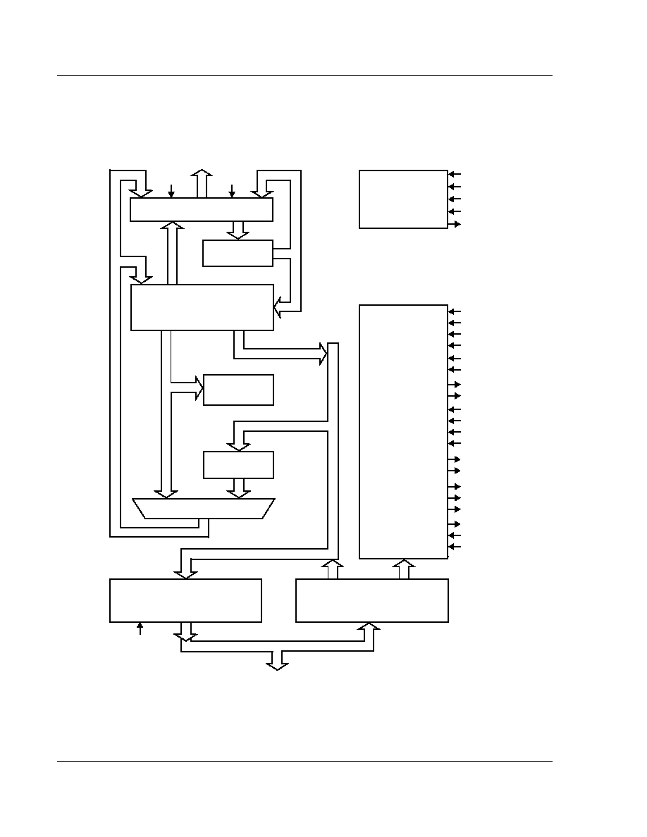
1.1 ARM60 Block diagram
Figure 1: ARM60 Block Diagram
LATEABT
A
nRESET
nMREQ
SEQ
ABORT
nIRQ
nFIQ
nRW
nBW
LOCK
nCPI
CPA
CPB
nWAIT
MCLK
nOPC
nTRANS
DATA32
BIGEND
PROG32
Instruction
Decoder
&
Control
Logic
Instruction Pipeline
& Read Data Register
DBE
D[31:0]
32 bit ALU
Barrel
Shifter
A
Address
Incrementer
Address Register
Register Bank
(31 x 32bit registers)
(6 status registers)
A[31:0]
ALE
I
n
c
r
e
m
e
n
t
e
r
B
u
s
P
C
B
u
s
L
U
B
u
s
b
u
s
B
b
u
s
Multiplier
ABE
Write Data Register
TCK
TMS
TDI
nTRST
TDO
Boundary
Scan
Logic
nM[4:0]
Booth�s
Introduction
3
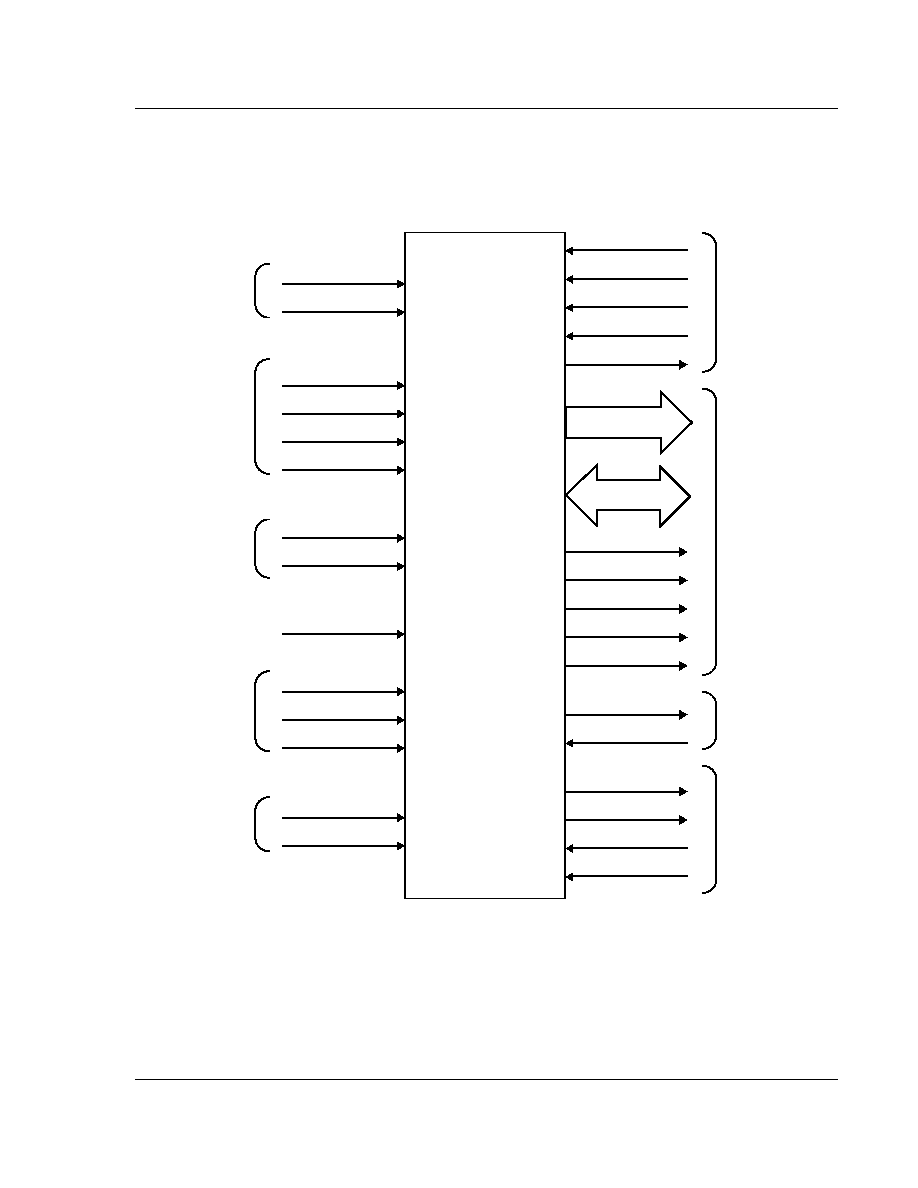
1.2 ARM60 Functional Diagram
Figure 2: ARM60 Functional Diagram
DBE
ABE
nIRQ
nFIQ
Bus
Interrupts
nRESET
MCLK
nWAIT
Clocks
VDD
VSS
Power
nRW
nBW
LOCK
A[31:0]
nMREQ
SEQ
ABORT
Memory
Management
nOPC
nCPI
CPA
CPB
Controls
Coprocessor
Interface
nTRANS
Memory
Interface
Interface
PROG32
DATA32
BIGEND
LATEABT
Configuration
D[31:0]
ALE
TCK
TMS
TDI
nTRST
Boundary
Scan
TDO
ARM60

P60ARM-B
4

Signal Description
5
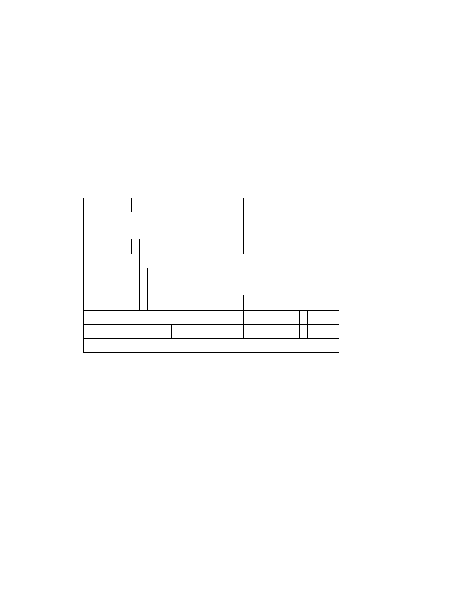
2.0 Signal Description
Name
Type
Description
A[31:0]
OS8
Addresses. This is the processor address bus. If
ALE
(address latch enable) is HIGH, the
addresses become valid during phase 2 of the cycle before the one to which they refer and
remain so during phase 1 of the referenced cycle. Their stable period may be controlled by
ALE
as described below. Refer to section "AC parameters" for timing diagrams.
ABE
I
Address bus enable. This is an input signal which, when LOW, puts the address bus drivers
into a high impedance state.
ABE
must be tied HIGH when there is no system requirement
to turn off the address drivers.
ABORT
I
Memory
ABORT
. This is an input which allows the memory system to tell the processor that
a requested access is not allowed. ARM60 can be configured to accept either early aborts for
compatibility with earlier processors or late aborts for greater flexibility.
ALE
I
Address latch enable. This input is used to control transparent latches on the address outputs.
Normally the addresses change during phase 2 to the value required during the next cycle,
but for direct interfacing to ROMs they are required to be stable to the end of phase 2. Taking
ALE
LOW until the end of phase 2 will ensure that this happens. If the system does not
require address lines to be held in this way,
ALE
must be tied HIGH. The address latch is
static, so
ALE
may be held LOW for long periods to freeze addresses.
BIGEND
I
Big Endian configuration. When this signal is HIGH the processor treats bytes in memory as
being in Big Endian format. When it is LOW memory is treated as Little
Endian.
CPA
I
Coprocessor absent. A coprocessor which is capable of performing the operation that ARM60
is requesting (by asserting
nCPI
) should take
CPA
LOW immediately. If
CPA
is HIGH at the
end of phase 1 of the cycle in which
nCPI
went LOW, ARM60 will
abort the coprocessor
handshake and take the undefined instruction trap. If
CPA
is LOW and remains LOW,
ARM60 will busy-wait until
CPB
is LOW and then complete the coprocessor instruction.
CPB
I
Coprocessor busy. A coprocessor which is capable of performing the operation which
ARM60 is requesting (by asserting
nCPI
), but cannot commit to starting it immediately,
should indicate this by driving
CPB
HIGH. When the coprocessor is ready to start it should
take
CPB
LOW. ARM60 samples
CPB
at the end of phase 1 of each cycle in which
nCPI
is
LOW.
D[31:0]
I/
OS8
Data Bus. These are bidirectional signal paths which are used for data transfers between the
processor and external memory. During read cycles (when
nRW
is LOW), the input data
must be valid before the end of phase 2 of the transfer cycle. During write cycles (when
nRW
is HIGH), the output data will become valid during phase 1 and remain valid throughout
phase 2 of the transfer cycle.
DATA32
I
32 bit Data configuration. When this signal is HIGH the processor can access data in a 32 bit
address space using address lines
A[31:0]
. When it is LOW the processor can access data from
a 26 bit address space using
A[25:0]
. In this latter configuration the address lines
A[31:26]
are
not used. Before changing
DATA32
, ensure that the processor is not about to access an
address greater that 0x3FFFFFF in the next cycle.
Table 1: Signal Description

P60ARM-B
6
DBE
I
Data bus enable. When
DBE
is LOW the write data register output drivers are disabled.
When
DBE
goes HIGH these output drivers are enabled.
DBE
facilitates data bus sharing for
DMA and so on.
LATEABT
I
Late
abort. This signal controls the action of the processor on an
abort exception. When it is
HIGH (Late
abort) the modified base register of an
aborted LDR or STR instruction is written
back. When it is LOW (Early abort) the modified base register is not written back.
LATEABT
must not be changed during the execution of a data access instruction where abort is active.
It is recommended that the Late
abort scheme be used where possible as this scheme will be
used in future ARM processors.
LOCK
OS8
Locked operation. When
LOCK
is HIGH, the processor is performing a �locked� memory
access, and the memory controller must wait until
LOCK
goes LOW before allowing another
device to access the memory.
LOCK
changes while
MCLK
is HIGH, and remains HIGH for
the duration of the locked memory accesses. It is active only during the data swap (SWP)
instruction.
MCLK
I
Memory clock input. This clock times all ARM60 memory accesses and internal operations.
The clock has two distinct phases -
phase 1
in which
MCLK
is LOW and
phase 2
in which
MCLK
(and
nWAIT
) is HIGH. The clock may be stretched indefinitely in either phase to
allow access to slow peripherals or memory. Alternatively, the
nWAIT
input may be used
with a free running
MCLK
to achieve the same effect.
nBW
OS8
Not byte/word. This is an output signal used by the processor to indicate to the external
memory system when a data transfer of a byte length is required. The signal is HIGH for
word transfers and LOW for byte transfers and is valid for both read and write cycles. The
signal will become valid during phase 2 of the cycle before the one in which the transfer will
take place. It will remain stable throughout phase 1 of the transfer cycle.
nCPI
O4
Not Coprocessor instruction. When ARM60 executes a coprocessor instruction, it will take
this output LOW and wait for a response from the coprocessor. The action taken will depend
on this response, which the coprocessor signals on the
CPA
and
CPB
inputs.
nFIQ
I
Not fast interrupt request. This is an asynchronous interrupt request to the processor which
causes it to be interrupted if taken LOW when the appropriate enable in the processor is
active. The signal is level sensitive and must be held LOW until a suitable response is
received from the processor.
nIRQ
I
Not interrupt request. As
nFIQ
, but with lower priority. May be taken LOW asynchronously
to interrupt the processor when the appropriate enable is active.
nMREQ
O4
Not memory request. This signal, when LOW, indicates that the processor requires memory
access during the following cycle. The signal becomes valid during phase 1, remaining valid
through phase 2 of the cycle preceding that to which it refers.
nOPC
O4
Not op-code fetch. When LOW this signal indicates that the processor is fetching an
instruction from memory; when HIGH, data (if present) is being transferred. The signal
becomes valid during phase 2 of the previous cycle, remaining valid through phase 1 of the
referenced cycle.
Name
Type
Description
Table 1: Signal Description

Signal Description
7
nRESET
I
Not reset. This is a level sensitive input signal which is used to start the processor from a
known address. A LOW level will cause the instruction being executed to terminate
abnormally. When
nRESET
becomes HIGH for at least one clock cycle, the processor will re-
start from address 0.
nRESET
must remain LOW (and
nWAIT
must remain HIGH) for at
least two clock cycles. During the LOW period the processor will perform dummy instruction
fetches with the address incrementing from the point where reset was activated. The address
will overflow to zero if
nRESET
is held beyond the maximum address limit.
nRW
OS8
Not read/write.When HIGH this signal indicates a processor write cycle; when LOW, a read
cycle. It becomes valid during phase 2 of the cycle before that to which it refers, and remains
valid to the end of phase 1 of the referenced cycle.
nTRANS
OS8
Not memory translate. When this signal is LOW it indicates that the processor is in user
mode. It may be used to tell memory management hardware when translation of the
addresses should be turned on, or as an indicator of non-user mode activity.
nTRST
IP
NOT Test Reset. Active-low reset signal for the boundary scan logic. This pin must be pulsed
or driven low to achieve normal device operation, in addition to the normal device reset
(nRESET). The action of this and the other four boundary scan signals are described in more
detail later in this document.
nWAIT
I
Not wait. When accessing slow peripherals, ARM60 can be made to wait for an integer
number of
MCLK
cycles by driving
nWAIT
LOW. Internally,
nWAIT
is ANDed with
MCLK
and must only change when
MCLK
is LOW. If
nWAIT
is not used it must be tied HIGH.
PROG32
I
32 bit Program configuration. When this signal is HIGH the processor can fetch instructions
from a 32 bit address space using address lines
A[31:0]
. When it is LOW the processor fetches
instructions from a 26 bit address space using
A[25:0]
. In this latter configuration the address
lines
A[31:26]
are not used for instruction fetches. Before changing
PROG32
, ensure that the
processor is in a 26 bit mode, and is not about to write to an address in the range 0 to 0x1F
(inclusive) in the next cycle.
SEQ
O4
Sequential address. This output signal will become HIGH when the address of the next
memory cycle will be related to that of the last memory access. The new address will either
be the same as or 4 greater than the old one.
The signal becomes valid during phase 1 and remains so through phase 2 of the cycle before
the cycle whose address it anticipates. It may be used, in combination with the low-order
address lines, to indicate that the next cycle can use a fast memory mode (for example DRAM
page mode) and/or to bypass the address translation system.
TCK
IP
Test Clock.
TDI
IP
Test Data Input.
TDO
OS8
Test Data Output. Output from the boundary scan logic.
TMS
IP
Test Mode Select.
VDD
P
Power supply. These connections provide power to the device.
VSS
P
Ground. These connections are the ground reference for all signals.
Name
Type
Description
Table 1: Signal Description

P60ARM-B
8
Key to Signal Types:
I
- Input
IP
- Input with pull-up resistor (35k
- 100k
)
O4 -
Output (4mA drive)
OS8
- slew-limited output (8mA drive)
P
- Power

Programmer's Model
9
3.0 Programmer's Model
ARM60 supports a variety of operating configurations. Some are controlled by inputs and are known as the
hardware configurations
. Others may be controlled by software and these are known as
operating modes
.
3.1 Hardware Con�guration
The ARM60 processor provides 4 hardware configurations which may be changed while the processor is
running and which are detailed in
Chapter 4.0 Instruction Set.
The
BIGEND
input sets whether the
ARM60 treats words in memory as being stored in Big Endian or Little
Endian format. Memory is viewed as a linear collection of bytes numbered upwards from zero. Bytes 0 to
3 hold the first stored word, bytes 4 to 7 the second and so on.
In the Little Endian scheme the lowest numbered byte in a word is considered to be the least significant byte
of the word and the highest numbered byte is the most significant. Byte 0 of the memory system should be
connected to data lines 7 through 0 (
D[7:0]
) in this scheme.
In the Big Endian scheme the most significant byte of a word is stored at the lowest numbered byte and the
least significant byte is stored at the highest numbered byte. Byte 0 of the memory system should therefore
be connected to data lines 31 through 24 (
D[31:24]
).
The
LATEABT
input sets the processor's behaviour when a data abort exception occurs. It only affects the
behaviour of load/store register instructions and is discussed more fully in
Chapter 3.0 Programmer's Model
and
Chapter 4.0 Instruction Set
.
The other two inputs,
PROG32
and
DATA32
are used for backward compatibility with earlier ARM
processors (see
13.0 Appendix - Backward Compatibility
) but should normally be set to 1. This configuration
extends the address space to 32 bits, introduces major changes in the programmer's model as described
below and provides support for running existing 26 bit programs in the 32 bit environment. This mode is
recommended for compatibility with future ARM processors and all new code should be written to use
only the 32 bit operating modes.
Because the original ARM instruction set has been modified to accommodate 32 bit operation there are
certain additional restrictions which programmers must be aware of. These are indicated in the text by the
words shall and shall not. Reference should also be made to the
ARM Application Notes �Rules for ARM Code
Writers�
and
�Notes for ARM Code Writers�
available from your supplier.
3.2 Operating Mode Selection
ARM60 has a 32 bit data bus and a 32 bit address bus. The data types the processor supports are Bytes (8
bits) and Words (32 bits), where words must be aligned to four byte boundaries. Instructions are exactly
one word, and data operations (e.g. ADD) are only performed on word quantities. Load and store
operations can transfer either bytes or words.

P60ARM-B
10
ARM60 supports six modes of operation:
(1)
User mode (usr): the normal program execution state
(2)
FIQ mode (fiq): designed to support a data transfer or channel process
(3)
IRQ mode (irq): used for general purpose interrupt handling
(4)
Supervisor mode (svc): a protected mode for the operating system
(5)
Abort mode (abt): entered after a data or instruction prefetch
abort
(6)
Undefined mode (und): entered when an undefined instruction is executed
Mode changes may be made under software control or may be brought about by external interrupts or
exception processing. Most application programs will execute in User mode. The other modes, known as
privileged modes
, will be entered to service interrupts or exceptions or to access protected resources.
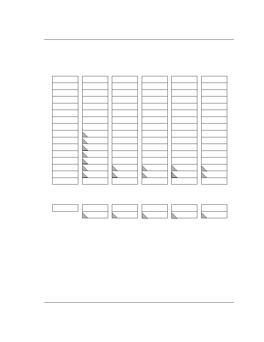
3.3 Registers
The processor has a total of 37 registers made up of 31 general 32 bit registers and 6 status registers. At any
one time 16 general registers (R0 to R15) and one or two status registers are visible to the programmer. The
visible registers depend on the processor mode and the other registers (the
banked registers
) are switched in
to support IRQ, FIQ, Supervisor,
Abort and Undefined mode processing. The register bank organisation is
shown in
Figure 3: Register Organisation
. The banked registers are shaded in the diagram.
In all modes 16 registers, R0 to R15, are directly accessible. All registers except R15 are general purpose and
may be used to hold data or address values. Register R15 holds the Program Counter (PC). When R15 is
read, bits [1:0] are zero and bits [31:2] contain the PC. A seventeenth register (the CPSR - Current Program
Status Register) is also accessible. It contains condition code flags and the current mode bits and may be
thought of as an extension to the PC.
R14 is used as the subroutine link register and receives a copy of R15 when a Branch and Link instruction
is executed. It may be treated as a general purpose register at all other times. R14_svc, R14_irq, R14_fiq,
R14_abt and R14_und are used similarly to hold the return values of R15 when interrupts and exceptions
arise, or when Branch and Link instructions are executed within interrupt or exception routines.
Programmer's Model
11
Figure 3: Register Organisation
FIQ mode has seven banked registers mapped to R8-14 (R8_fiq-R14_fiq). Many FIQ programs will not need
to save any registers. User mode, IRQ mode, Supervisor mode,
Abort mode and Undefined mode each have
two banked registers mapped to R13 and R14. The two banked registers allow these modes to each have a
private stack pointer and link register. Supervisor, IRQ,
Abort and Undefined mode programs which
require more than these two banked registers are expected to save some or all of the caller's registers (R0 to
R12) on their respective stacks. They are then free to use these registers which they will restore before
returning to the caller. In addition there are also five SPSRs (Saved Program Status Registers) which are
loaded with the CPSR when an exception occurs. There is one SPSR for each privileged mode. Thus the
CPSR of the calling mode can be easily restored when the current (privileged) mode is exited.
General Registers and Program Counter
R0
R1
R2
R3
R4
R5
R6
R7
R8
R9
R10
R11
R12
R13
R14
R15 (PC)
R0
R1
R2
R3
R4
R5
R6
R7
R8_fiq
R9_fiq
R10_fiq
R11_fiq
R12_fiq
R13_fiq
R14_fiq
R15 (PC)
R0
R1
R2
R3
R4
R5
R6
R7
R8
R9
R10
R11
R12
R13_svc
R14_svc
R15 (PC)
R0
R1
R2
R3
R4
R5
R6
R7
R8
R9
R10
R11
R12
R13_abt
R14_abt
R15 (PC)
R0
R1
R2
R3
R4
R5
R6
R7
R8
R9
R10
R11
R12
R13_irq
R14_irq
R15 (PC)
R0
R1
R2
R3
R4
R5
R6
R7
R8
R9
R10
R11
R12
R13_und
R14_und
R15 (PC)
User32
FIQ32
Supervisor32
Abort32
IRQ32
Undefined32
CPSR
CPSR
SPSR_fiq
CPSR
SPSR_svc
CPSR
SPSR_abt
CPSR
SPSR_irq
CPSR
SPSR_und
Program Status Registers
P60ARM-B
12
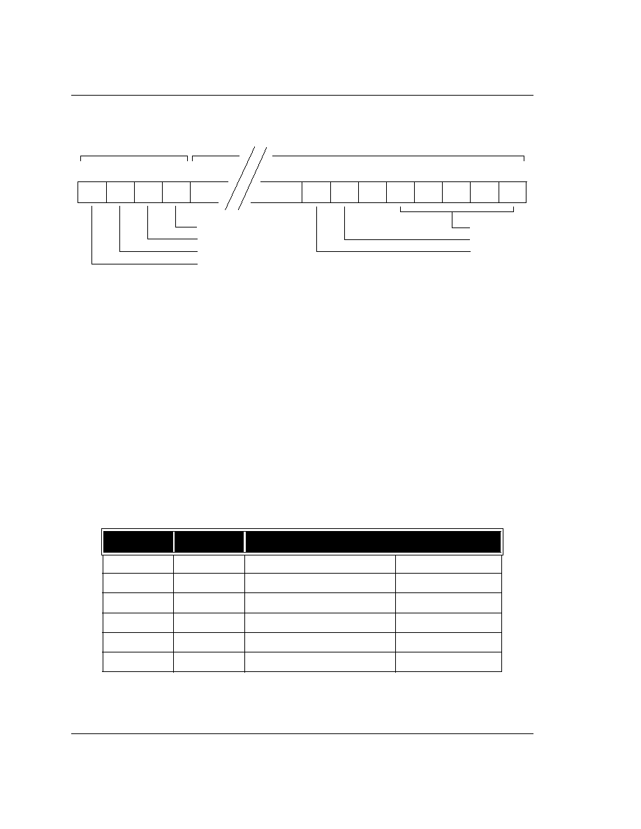
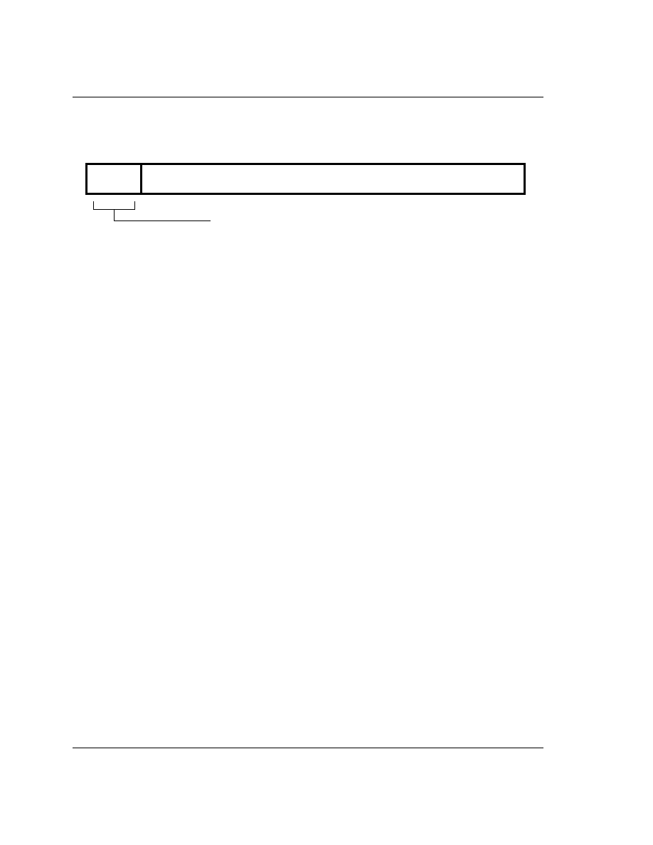
Figure 4:
Format of the Program Status Registers (PSRs)
The format of the Program Status Registers is shown in
Figure 4: Format of the Program Status Registers
(PSRs)
. The N, Z, C and V bits are the
condition code flags
. The condition code flags in the CPSR may be
changed as a result of arithmetic and logical operations in the processor and may be tested by all
instructions to determine if the instruction is to be executed.
The I and F bits are the
interrupt disable bits.
The I bit disables IRQ interrupts when it is set and the F bit
disables FIQ interrupts when it is set. The M0, M1, M2, M3 and M4 bits (M[4:0]) are the
mode bits
, and these
determine the mode in which the processor operates. The interpretation of the mode bits is shown in
Table
2: The Mode Bits
. Not all combinations of the mode bits define a valid processor mode. Only those explicitly
described shall be used.
The bottom 28 bits of a PSR (incorporating I, F and M[4:0]) are known collectively as the
control bits
. The
control bits will change when an exception arises and in addition can be manipulated by software when the
processor is in a privileged mode. Unused bits in the PSRs are reserved and their state shall be preserved
when changing the flag or control bits. Programs shall not rely on specific values from the reserved bits
when checking the PSR status, since they may read as one or zero in future processors.
M[4:0]
Mode
Accessible register set
10000
User
PC, R14..R0
CPSR
10001
FIQ
PC, R14_fiq..R8_fiq, R7..R0
CPSR, SPSR_fiq
10010
IRQ
PC, R14_irq..R13_irq, R12..R0
CPSR, SPSR_irq
10011
Supervisor
PC, R14_svc..R13_svc, R12..R0
CPSR, SPSR_svc
10111
Abort
PC, R14_abt..R13_abt, R12..R0
CPSR, SPSR_abt
11011
Undefined
PC, R14_und..R13_und, R12..R0
CPSR, SPSR_und
Table 2: The Mode Bits
0
1
2
3
4
5
6
7
8
27
28
29
30
31
M0
M1
M2
M3
M4
.
F
I
V
C
Z
N
Overflow
Carry / Borrow / Extend
Zero
Negative / Less Than
Mode bits
FIQ disable
IRQ disable
.
.
.
flags
control

Programmer's Model
13
3.4 Exceptions
Exceptions arise whenever there is a need for the normal flow of program execution to be broken, so that
(for example) the processor can be diverted to handle an interrupt from a peripheral. The processor state
just prior to handling the exception must be preserved so that the original program can be resumed when
the exception routine has completed. Many exceptions may arise at the same time.
ARM60 handles exceptions by making use of the banked registers to save state. The old PC and CPSR
contents are copied into the appropriate R14 and SPSR and the PC and mode bits in the CPSR bits are forced
to a value which depends on the exception. Interrupt disable flags are set where required to prevent
otherwise unmanageable nestings of exceptions. In the case of a re-entrant interrupt handler, R14 and the
SPSR should be saved onto a stack in main memory before re-enabling the interrupt; when transferring the
SPSR register to and from a stack, it is important to transfer the whole 32 bit value, and not just the flag or
control fields. When multiple exceptions arise simultaneously, a fixed priority determines the order in
which they are handled. The priorities are listed later in this chapter.
3.4.1 FIQ
The FIQ (Fast Interrupt reQuest) exception is externally generated by taking the
nFIQ
input LOW. This
input can accept asynchronous transitions, and is delayed by one clock cycle for synchronisation before it
can affect the processor execution flow. It is designed to support a data transfer or channel process, and has
sufficient private registers to remove the need for register saving in such applications (thus minimising the
overhead of context switching). The FIQ exception may be disabled by setting the F flag in the CPSR (but
note that this is not possible from User mode). If the F flag is clear, ARM60 checks for a LOW level on the
output of the FIQ synchroniser at the end of each instruction.
When a FIQ is detected, ARM60 performs the following:
(1)
Saves the address of the next instruction to be executed plus 4 in R14_fiq; saves CPSR in SPSR_fiq
(2)
Forces M[4:0]=10001 (FIQ mode) and sets the F and I bits in the CPSR
(3)
Forces the PC to fetch the next instruction from address 0x1C
To return normally from FIQ, use SUBS PC, R14_fiq,#4 which will restore both the PC (from R14) and the
CPSR (from SPSR_fiq) and resume execution of the interrupted code. R14_fiq is a symbol for the register
R14 and if used needs to be declared in the users application program.
3.4.2 IRQ
The IRQ (Interrupt ReQuest) exception is a normal interrupt caused by a LOW level on the
nIRQ
input. It
has a lower priority than FIQ, and is masked out when a FIQ sequence is entered. Its effect may be masked
out at any time by setting the I bit in the CPSR (but note that this is not possible from User mode). If the I
flag is clear, ARM60 checks for a LOW level on the output of the IRQ synchroniser at the end of each
instruction. When an IRQ is detected, ARM60 performs the following:
(1)
Saves the address of the next instruction to be executed plus 4 in R14_irq; saves CPSR in SPSR_irq
(2)
Forces M[4:0]=10010 (IRQ mode) and sets the I bit in the CPSR
(3)
Forces the PC to fetch the next instruction from address 0x18

P60ARM-B
14
To return normally from IRQ, use SUBS PC,R14_irq,#4 which will restore both the PC and the CPSR and
resume execution of the interrupted code. R14_fiq is a symbol for the register R14 and if used needs to be
declared in the users application program.
3.4.3 Abort
An
ABORT can be signalled by the external
ABORT
input. ABORT indicates that the current memory
access cannot be completed. For instance, in a virtual memory system the data corresponding to the current
address may have been moved out of memory onto a disc, and considerable processor activity may be
required to recover the data before the access can be performed successfully. ARM60 checks for ABORT
during memory access cycles. When successfully
aborted ARM60 will respond in one of two ways:
(1)
If the
abort occurred during an instruction prefetch (a
Prefetch
Abort
), the prefetched instruction is
marked as invalid but the
abort exception does not occur immediately. If the instruction is not
executed, for example as a result of a branch being taken while it is in the pipeline, no
abort will
occur. An
abort will take place if the instruction reaches the head of the pipeline and is about to be
executed.
(2)
If the
abort occurred during a data access (a
Dat
a
Abort
), the action depends on the instruction type.
(a) Single data transfer instructions (LDR, STR) are
aborted as though the instruction had not executed
if the processor is configured for Early
Abort. When configured for Late
Abort, these instructions
are able to write back modified base registers and the Abort handler must be aware of this.
(b) The swap instruction (SWP) is
aborted as though it had not executed, though externally the read
access may take place.
(c) Block data transfer instructions (LDM, STM) complete, and if write-back is set, the base is updated.
If the instruction would normally have overwritten the base with data (i.e. LDM with the base in
the transfer list), this overwriting is prevented. All register overwriting is prevented after the
Abort
is indicated, which means in particular that R15 (which is always last to be transferred) is preserved
in an aborted LDM instruction.
When either a prefetch or data abort occurs, ARM60 performs the following:
(1)
Saves the address of the
aborted instruction plus 4 (for prefetch
aborts) or 8 (for data aborts) in
R14_abt; saves CPSR in SPSR_abt.
(2)
Forces M[4:0]=10111 (Abort mode) and sets the I bit in the CPSR.
(3)
Forces the PC to fetch the next instruction from either address 0x0C (prefetch abort) or address 0x10
(data
abort).
To return after fixing the reason for the
abort, use SUBS PC,R14_abt,#4 (for a prefetch
abort) or SUBS
PC,R14_abt,#8 (for a data abort). This will restore both the PC and the CPSR and retry the
aborted
instruction. R14_fiq is a symbol for the register R14 and if used needs to be declared in the users application
program.
The
abort mechanism allows a
demand paged virtual memory system
to be implemented when suitable
memory management software is available. The processor is allowed to generate arbitrary addresses, and
when the data at an address is unavailable the MMU signals an
abort. The processor traps into system

Programmer's Model
15
software which must work out the cause of the
abort, make the requested data available, and retry the
aborted instruction. The application program needs no knowledge of the amount of memory available to
it, nor is its state in any way affected by the abort.
3.4.4 Software interrupt
The software interrupt instruction (SWI) is used for getting into Supervisor mode, usually to request a
particular supervisor function. When a SWI is executed, ARM60 performs the following:
(1)
Saves the address of the SWI instruction plus 4 in R14_svc; saves CPSR in SPSR_svc
(2)
Forces M[4:0]=10011 (Supervisor mode) and sets the I bit in the CPSR
(3)
Forces the PC to fetch the next instruction from address 0x08
To return from a SWI, use MOVS PC,R14_svc. This will restore the PC and CPSR and return to the
instruction following the SWI.
3.4.5 Unde�ned instruction trap
When the ARM60 comes across an instruction which it cannot handle (see
Chapter 4.0 Instruction Set
), it
offers it to any coprocessors which may be present. If a coprocessor can perform this instruction but is busy
at that time, ARM60 will wait until the coprocessor is ready or until an interrupt occurs. If no coprocessor
can handle the instruction then ARM60 will take the undefined instruction trap.
The trap may be used for software emulation of a coprocessor in a system which does not have the
coprocessor hardware, or for general purpose instruction set extension by software emulation.
When ARM60 takes the undefined instruction trap it performs the following:
(1)
Saves the address of the Undefined or coprocessor instruction plus 4 in R14_und; saves CPSR in
SPSR_und.
(2)
Forces M[4:0]=11011 (Undefined mode) and sets the I bit in the CPSR
(3)
Forces the PC to fetch the next instruction from address 0x04
To return from this trap after emulating the failed instruction, use MOVS PC,R14_und. This will restore the
CPSR and return to the instruction following the undefined instruction.

P60ARM-B
16
3.4.6 Vector Summary
These are byte addresses, and will normally contain a branch instruction pointing to the relevant routine.
The FIQ routine might reside at 0x1C onwards, and thereby avoid the need for (and execution time of) a
branch instruction.
The reserved entry is for an Address Exception vector which is only operative when the processor is
configured for a 26 bit program space. See
13.0 Appendix - Backward Compatibility
3.4.7 Exception Priorities
When multiple exceptions arise at the same time, a fixed priority system determines the order in which they
will be handled:
(1)
Reset (highest priority)
(2)
Data abort
(3)
FIQ
(4)
IRQ
(5)
Prefetch abort
(6)
Undefined Instruction, Software interrupt (lowest priority)
Note that not all exceptions can occur at once. Undefined instruction and software interrupt are mutually
exclusive since they each correspond to particular (non-overlapping) decodings of the current instruction.
If a data abort
occurs at the same time as a FIQ, and FIQs are enabled (i.e. the F flag in the CPSR is clear),
ARM60 will enter the data abort handler and then immediately proceed to the FIQ vector. A normal return
from FIQ will cause the data abort handler to resume execution. Placing data abort at a higher priority than
FIQ is necessary to ensure that the transfer error does not escape detection; the time for this exception entry
should be added to worst case FIQ latency calculations.
Address
Exception
Mode on entry
0x00000000
Reset
Supervisor
0x00000004
Unde�ned instruction
Unde�ned
0x00000008
Software interrupt
Supervisor
0x0000000C
Abort (prefetch)
Abort
0x00000010
Abort (data)
Abort
0x00000014
-- reserved --
--
0x00000018
IRQ
IRQ
0x0000001C
FIQ
FIQ
Table 3: Vector Summary

Programmer's Model
17
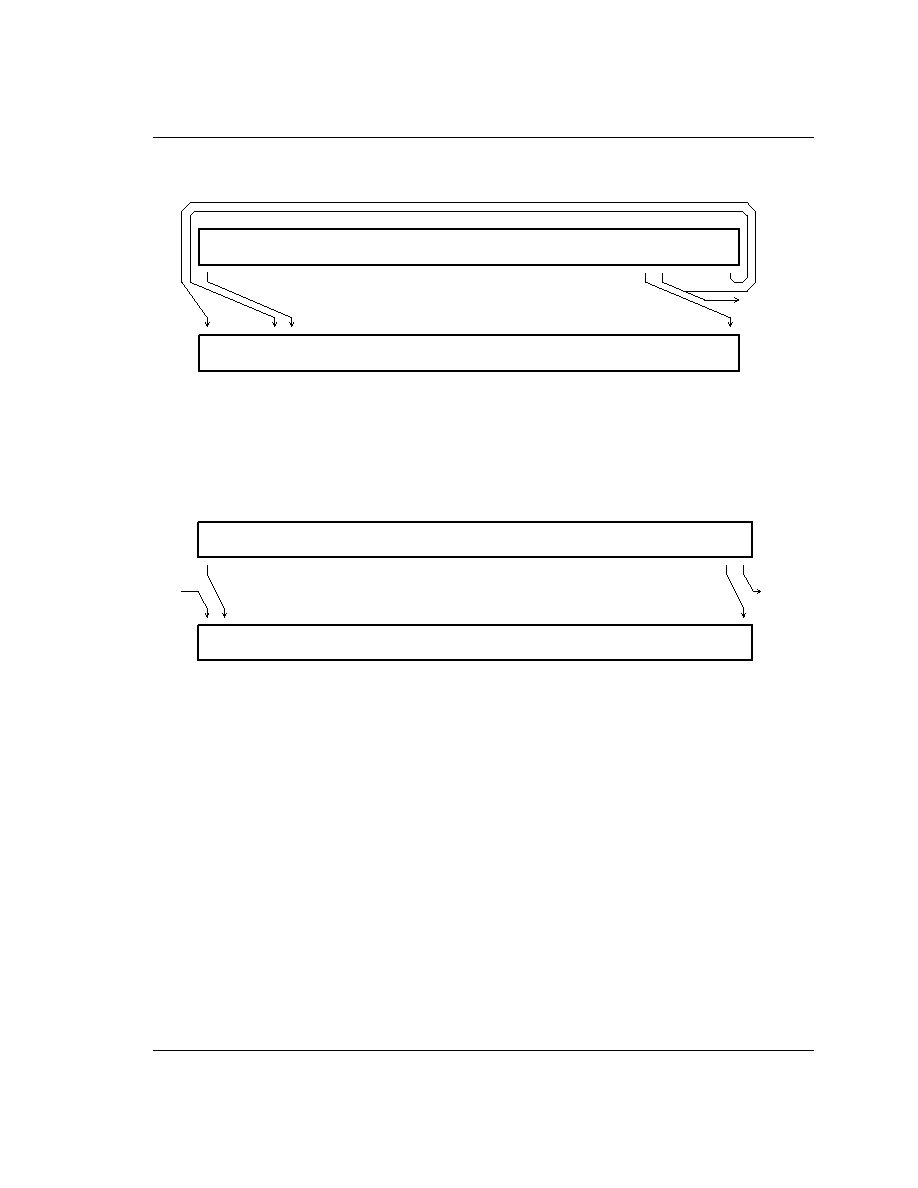
3.4.8 Interrupt Latencies
The worst case latency for FIQ, assuming that it is enabled, consists of the longest time the request can take
to pass through the synchroniser (
Tsyncmax
), plus the time for the longest instruction to complete (
Tldm
, the
longest instruction is an LDM which loads all the registers including the PC), plus the time for the data abort
entry (
Texc
), plus the time for FIQ entry (
Tfiq
). At the end of this time ARM60 will be executing the
instruction at 0x1C.
Tsyncmax
is 3 processor cycles,
Tldm
is 20 cycles,
Texc
is 3 cycles, and
Tfiq is 2 cycles. The total time is
therefore 28 processor cycles. This is just over 1.4 microseconds in a system which uses a continuous 20
MHz processor clock. The maximum IRQ latency calculation is similar, but must allow for the fact that FIQ
has higher priority and could delay entry into the IRQ handling routine for an arbitrary length of time. The
minimum latency for FIQ or IRQ consists of the shortest time the request can take through the synchroniser
(Tsyncmin) plus Tfiq. This is 4 processor cycles.
To reduce the interupt latency, Tldm can be reduced by using an option in the complier which splits LDM
instructions so that it will only load or store a user defined number (between 3 and 16) of registers at any
one time.
If this option is used, then the MUL or MLA instruction can potentially become the longest taking up to 17
cycles, depending on the data being manipulated.
3.5 Reset
When the nRESET signal goes LOW, ARM60 abandons the executing instruction and then continues to
fetch instructions from incrementing word addresses.
When nRESET goes HIGH again, ARM60 does the following:
(1)
Overwrites R14_svc and SPSR_svc by copying the current values of the PC and CPSR into them.
The value of the saved PC and CPSR is not defined.
(2)
Forces M[4:0]=10011 (Supervisor mode) and sets the I and F bits in the CPSR.
(3)
Forces the PC to fetch the next instruction from address 0x00

P60ARM-B
18
Instruction Set - Summary
19
4.0 Instruction Set
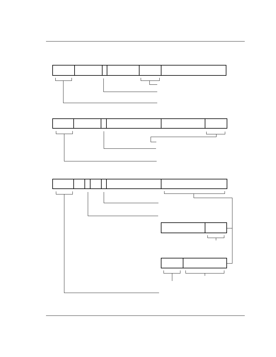
4.1 Instruction Set Summary
A summary of the ARM60 instruction set is shown in
Figure 5: Instruction Set Summary
.
Note:
some instruction codes are not defined but do not cause the Undefined instruction trap to be taken,
for instance a Multiply instruction with bit 6 changed to a 1. These instructions shall not be used,
as their action may change in future ARM implementations.
Figure 5: Instruction Set Summary
31
28 27
24 23
20 19
16 15
12 11
8
7
5
4
3
0
Cond
0 0
Opcode
21
S
Rn
Rd
Operand 2
Data Processing
PSR Transfer
Multiply
Single Data Swap
Single Data Transfer
Undefined
Block Data Transfer
Coproc Data Transfer
Branch
Coproc Data Operation
Coproc Register Transfer
Software Interrupt
26 25
22
I
Cond
Cond
Cond
Cond
Cond
Cond
Cond
Cond
Cond
Cond
0 0 0 0 0 0
S
A
Rd
Rn
Rs
1 0 0 1
Rm
1 0 0 1
Rm
0 0 0 0
Rd
Rn
0 0 0 1 0
B
0 0
offset
Rd
Rn
B W L
I
P U
0 1
0 1 1
XXXXXXXXXXXXXXXXXXXX
1
XXXX
1 0 0
S W L
P U
Rn
Register List
1 0 1
L
1 1 0
offset
1 1 1 0
0
CRm
1 1 1 0
L
CP Opc
N W L
P U
Rn
offset
CRd
CP#
1 1 1 1
CP Opc
CRn
CRd
CRn
Rd
CP#
CP#
CP
CP
1
CRm
ignored by processor
P60ARM-B
20
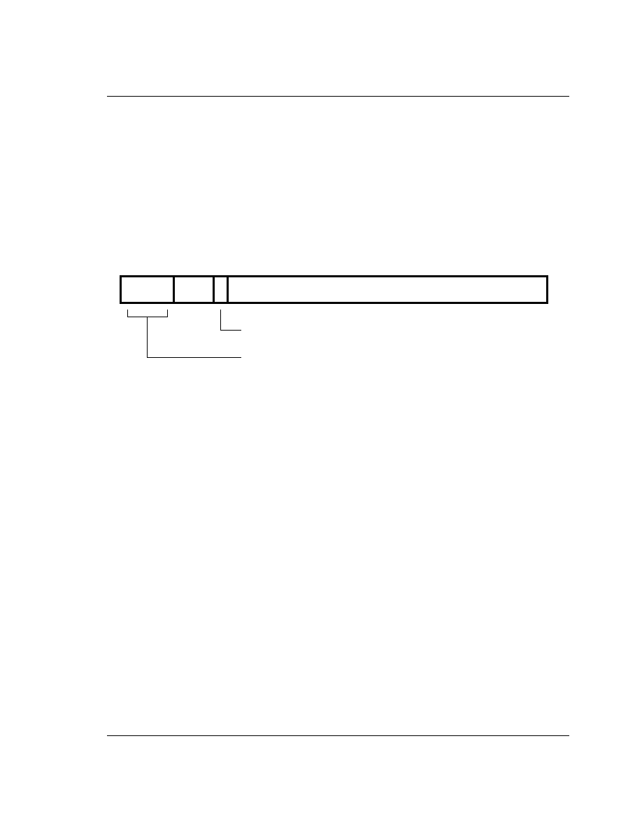
4.2 The Condition Field
Figure 6: Condition Codes
All ARM60 instructions are conditionally executed, which means that their execution may or may not take
place depending on the values of the N, Z, C and V flags in the CPSR. The condition encoding is shown in
Figure 6: Condition Codes
.
If the
always
(AL) condition is specified, the instruction will be executed irrespective of the flags. The
never
(NV) class of condition codes shall not be used as they will be redefined in future variants of the ARM
architecture. If a NOP is required it is suggested that MOV R0,R0 be used. The assembler treats the absence
of a condition code as though
always
had been specified.
The other condition codes have meanings as detailed in
Figure 6: Condition Codes
, for instance code 0000
(EQual) causes the instruction to be executed only if the Z flag is set. This would correspond to the case
where a compare (CMP) instruction had found the two operands to be equal. If the two operands were
different, the compare instruction would have cleared the Z flag and the instruction will not be executed.
Cond
31
28 27
0
Condition field
0000 = EQ - Z set (equal)
0001 = NE - Z clear (not equal)
0010 = CS - C set (unsigned higher or same)
0011 = CC - C clear (unsigned lower)
0100 = MI - N set (negative)
0101 = PL - N clear (positive or zero)
0110 = VS - V set (overflow)
0111 = VC - V clear (no overflow)
1000 = HI - C set and Z clear (unsigned higher)
1001 = LS - C clear or Z set (unsigned lower or same)
1010 = GE - N set and V set, or N clear and V clear (greater or equal)
1011 = LT - N set and V clear, or N clear and V set (less than)
1100 = GT - Z clear, and either N set and V set, or N clear and V clear (greater than)
1101 = LE - Z set, or N set and V clear, or N clear and V set (less than or equal)
1110 = AL - always
1111 = NV - never
Instruction Set - B, BL
21
4.3 Branch and Branch with link (B, BL)
The instruction is only executed if the condition is true. The various conditions are defined at the beginning
of this chapter. The instruction encoding is shown in
Figure 7: Branch Instructions
.
Branch instructions contain a signed 2's complement 24 bit offset. This is shifted left two bits, sign extended
to 32 bits, and added to the PC. The instruction can therefore specify a branch of +/- 32Mbytes. The branch
offset must take account of the prefetch operation, which causes the PC to be 2 words (8 bytes) ahead of the
current instruction.
Figure 7: Branch Instructions
Branches beyond +/- 32Mbytes must use an offset or absolute destination which has been previously
loaded into a register. In this case the PC should be manually saved in R14 if a Branch with Link type
operation is required.
4.3.1 The link bit
Branch with Link (BL) writes the old PC into the link register (R14) of the current bank. The PC value
written into R14 is adjusted to allow for the prefetch, and contains the address of the instruction following
the branch and link instruction. Note that the CPSR is not saved with the PC.
To return from a routine called by Branch with Link use MOV PC,R14 if the link register is still valid or
LDM Rn!,{..PC} if the link register has been saved onto a stack pointed to by Rn.
4.3.2 Instruction Cycle Times
Branch and Branch with Link instructions take 2S + 1N incremental cycles, where S and N are as defined in
section 5.1 Cycle types on page 65.
4.3.3 Assembler syntax
B{L}{cond} <expression>
{L} is used to request the Branch with Link form of the instruction. If absent, R14 will not be affected by the
instruction.
{cond} is a two-char mnemonic as shown in
Figure 6: Condition Codes
(EQ, NE, VS etc). If absent then AL
(ALways) will be used.
Cond
101
L
offset
31
28 27
25 24 23
0
Link bit
0 = Branch
1 = Branch with Link
Condition field

P60ARM-B
22
<expression> is the destination. The assembler calculates the offset.
Items in {} are optional. Items in <> must be present.
4.3.4 Examples
here
BAL
here
; assembles to 0xEAFFFFFE (note effect of PC offset)
B
there
; ALways condition used as default
CMP
R1,#0
; compare R1 with zero and branch to fred if R1
BEQ
fred
; was zero otherwise continue to next instruction
BL
sub+ROM
; call subroutine at computed address
ADDS
R1,#1
; add 1 to register 1, setting CPSR flags on the
BLCC
sub
; result then call subroutine if the C flag is clear,
; which will be the case unless R1 held 0xFFFFFFFF

Instruction Set - Data processing
23
4.4 Data
processing
The instruction is only executed if the condition is true, defined at the beginning of this chapter. The
instruction encoding is shown in
Figure 8: Data Processing Instructions
.
The instruction produces a result by performing a specified arithmetic or logical operation on one or two
operands. The first operand is always a register (Rn). The second operand may be a shifted register (Rm) or
a rotated 8 bit immediate value (Imm) according to the value of the I bit in the instruction. The condition
codes in the CPSR may be preserved or updated as a result of this instruction, according to the value of the
S bit in the instruction. Certain operations (TST, TEQ, CMP, CMN) do not write the result to Rd. They are
used only to perform tests and to set the condition codes on the result and always have the S bit set. The
instructions and their effects are listed in
Table 4: ARM Data Processing Instructions
.
Figure 8: Data Processing Instructions
Cond
00
I
OpCode
Rn
Rd
Operand 2
0
11
12
15
16
19
20
21
24
25
26
27
28
31
Destination register
1st operand register
Set condition codes
Operation Code
0 = do not alter condition codes
1 = set condition codes
0000 = AND - Rd:= Op1 AND Op2
0010 = SUB - Rd:= Op1 - Op2
0011 = RSB - Rd:= Op2 - Op1
0100 = ADD - Rd:= Op1 + Op2
0101 = ADC - Rd:= Op1 + Op2 + C
0110 = SBC - Rd:= Op1 - Op2 + C
0111 = RSC - Rd:= Op2 - Op1 + C
1000 = TST - set condition codes on Op1 AND Op2
1001 = TEQ - set condition codes on Op1 EOR Op2
1010 = CMP - set condition codes on Op1 - Op2
1011 = CMN - set condition codes on Op1 + Op2
1100 = ORR - Rd:= Op1 OR Op2
1101 = MOV - Rd:= Op2
1110 = BIC - Rd:= Op1 AND NOT Op2
1111 = MVN - Rd:= NOT Op2
Immediate Operand
0 = operand 2 is a register
1 = operand 2 is an immediate value
Shift
Rm
Rotate
S
Unsigned 8 bit immediate value
2nd operand register
shift applied to Rm
shift applied to Imm
Imm
Condition field
11
8
7
0
0
3
4
11
0001 = EOR - Rd:= Op1 EOR Op2
- 1
- 1

P60ARM-B
24
4.4.1 CPSR �ags
The data processing operations may be classified as logical or arithmetic. The logical operations (AND,
EOR, TST, TEQ, ORR, MOV, BIC, MVN) perform the logical action on all corresponding bits of the operand
or operands to produce the result. If the S bit is set (and Rd is not R15, see below) the V flag in the CPSR will
be unaffected, the C �ag will be set to the carry out from the barrel shifter (or preserved when the shift
operation is LSL #0), the Z �ag will be set if and only if the result is all zeros, and the N �ag will be set to
the logical value of bit 31 of the result
.
The arithmetic operations (SUB, RSB, ADD, ADC, SBC, RSC, CMP, CMN) treat each operand as a 32 bit
integer (either unsigned or 2's complement signed, the two are equivalent). If the S bit is set (and Rd is not
R15) the V flag in the CPSR will be set if an overflow occurs into bit 31 of the result; this may be ignored if
the operands were considered unsigned, but warns of a possible error if the operands were 2's complement
signed. The C flag will be set to the carry out of bit 31 of the ALU, the Z flag will be set if and only if the
result was zero, and the N flag will be set to the value of bit 31 of the result (indicating a negative result if
the operands are considered to be 2's complement signed).
Assembler
Mnemonic
OpCode
Action
AND
0000
operand1 AND operand2
EOR
0001
operand1 EOR operand2
SUB
0010
operand1 - operand2
RSB
0011
operand2 - operand1
ADD
0100
operand1 + operand2
ADC
0101
operand1 + operand2 + carry
SBC
0110
operand1 - operand2 + carry - 1
RSC
0111
operand2 - operand1 + carry - 1
TST
1000
as AND, but result is not written
TEQ
1001
as EOR, but result is not written
CMP
1010
as SUB, but result is not written
CMN
1011
as ADD, but result is not written
ORR
1100
operand1 OR operand2
MOV
1101
operand2 (operand1 is ignored)
BIC
1110
operand1 AND NOT operand2 (Bit clear)
MVN
1111
NOT operand2 (operand1 is ignored)
Table 4: ARM Data Processing Instructions

Instruction Set - Shifts
25
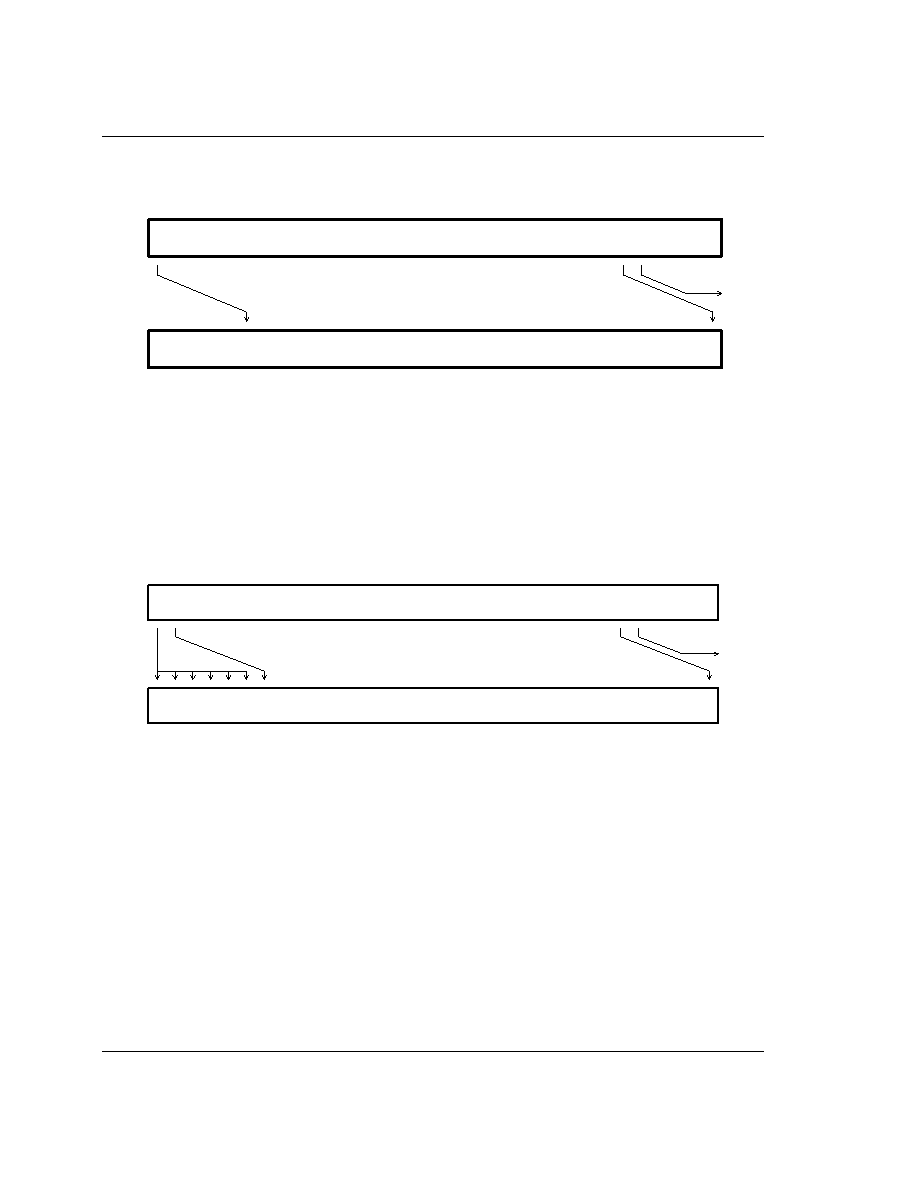
4.4.2 Shifts
When the second operand is specified to be a shifted register, the operation of the barrel shifter is controlled
by the Shift field in the instruction. This field indicates the type of shift to be performed (logical left or right,
arithmetic right or rotate right). The amount by which the register should be shifted may be contained in
an immediate field in the instruction, or in the bottom byte of another register (other than R15). The
encoding for the different shift types is shown in
Figure 9: ARM Shift Operations
.
Figure 9: ARM Shift Operations
Instruction specified shift amount
When the shift amount is specified in the instruction, it is contained in a 5 bit field which may take any value
from 0 to 31. A logical shift left (LSL) takes the contents of Rm and moves each bit by the specified amount
to a more significant position. The least significant bits of the result are filled with zeros, and the high bits
of Rm which do not map into the result are discarded, except that the least significant discarded bit becomes
the shifter carry output which may be latched into the C bit of the CPSR when the ALU operation is in the
logical class (see above). For example, the effect of LSL #5 is shown in
Figure 10: Logical Shift Left
.
Figure 10: Logical Shift Left
Note that LSL #0 is a special case, where the shifter carry out is the old value of the CPSR C flag. The
contents of Rm are used directly as the second operand.
A logical shift right (LSR) is similar, but the contents of Rm are moved to less significant positions in the
result. LSR #5 has the effect shown in Figure 11: Logical Shift Right.
0
0
1
Rs
11
8
7
6
5
4
11
7 6
5
4
Shift type
Shift amount
5 bit unsigned integer
00 = logical left
01 = logical right
10 = arithmetic right
11 = rotate right
Shift type
Shift register
00 = logical left
01 = logical right
10 = arithmetic right
11 = rotate right
Shift amount specified in
bottom byte of Rs
0 0 0 0 0
contents of Rm
value of operand 2
31
27 26
0
carry out
P60ARM-B
26
Figure 11: Logical Shift Right
The form of the shift field which might be expected to correspond to LSR #0 is used to encode LSR #32,
which has a zero result with bit 31 of Rm as the carry output. Logical shift right zero is redundant as it is
the same as logical shift left zero, so the assembler will convert LSR #0 (and ASR #0 and ROR #0) into LSL
#0, and allow LSR #32 to be specified.
An arithmetic shift right (ASR) is similar to logical shift right, except that the high bits are filled with bit 31
of Rm instead of zeros. This preserves the sign in 2's complement notation. For example, ASR #5 is shown
in Figure 12: Arithmetic Shift Right.
Figure 12: Arithmetic Shift Right
The form of the shift field which might be expected to give ASR #0 is used to encode ASR #32. Bit 31 of Rm
is again used as the carry output, and each bit of operand 2 is also equal to bit 31 of Rm. The result is
therefore all ones or all zeros, according to the value of bit 31 of Rm.
Rotate right (ROR) operations reuse the bits which 'overshoot' in a logical shift right operation by
reintroducing them at the high end of the result, in place of the zeros used to fill the high end in logical right
operations. For example, ROR #5 is shown in Figure 13: Rotate Right.
contents of Rm
value of operand 2
31
0
carry out
0 0 0 0 0
5
4
contents of Rm
value of operand 2
31
0
carry out
5
4
30
Instruction Set - Shifts
27
Figure 13: Rotate Right
The form of the shift field which might be expected to give ROR #0 is used to encode a special function of
the barrel shifter, rotate right extended (RRX). This is a rotate right by one bit position of the 33 bit quantity
formed by appending the CPSR C flag to the most significant end of the contents of Rm as shown in Figure
14: Rotate Right Extended.
Figure 14: Rotate Right Extended
Register specified shift amount
Only the least significant byte of the contents of Rs is used to determine the shift amount. Rs can be any
general register other than R15.
If this byte is zero, the unchanged contents of Rm will be used as the second operand, and the old value of
the CPSR C flag will be passed on as the shifter carry output.
If the byte has a value between 1 and 31, the shifted result will exactly match that of an instruction specified
shift with the same value and shift operation.
If the value in the byte is 32 or more, the result will be a logical extension of the shift described above:
(1)
LSL by 32 has result zero, carry out equal to bit 0 of Rm.
(2)
LSL by more than 32 has result zero, carry out zero.
(3)
LSR by 32 has result zero, carry out equal to bit 31 of Rm.
(4)
LSR by more than 32 has result zero, carry out zero.
contents of Rm
value of operand 2
31
0
carry out
5 4
contents of Rm
value of operand 2
31
0
carry
out
1
C
in

P60ARM-B
28
(5)
ASR by 32 or more has result filled with and carry out equal to bit 31 of Rm.
(6)
ROR by 32 has result equal to Rm, carry out equal to bit 31 of Rm.
(7)
ROR by n where n is greater than 32 will give the same result and carry out as ROR by n-32;
therefore repeatedly subtract 32 from n until the amount is in the range 1 to 32 and see above.
Note that the zero in bit 7 of an instruction with a register controlled shift is compulsory; a one in this bit
will cause the instruction to be a multiply or undefined instruction.
4.4.3 Immediate operand rotates
The immediate operand rotate field is a 4 bit unsigned integer which specifies a shift operation on the 8 bit
immediate value. This value is zero extended to 32 bits, and then subject to a rotate right by twice the value
in the rotate field. This enables many common constants to be generated, for example all powers of 2.
4.4.4 Writing to R15
When Rd is a register other than R15, the condition code flags in the CPSR may be updated from the ALU
flags as described above.
When Rd is R15 and the S flag in the instruction is not set the result of the operation is placed in R15 and
the CPSR is unaffected.
When Rd is R15 and the S flag is set the result of the operation is placed in R15 and the SPSR corresponding
to the current mode is moved to the CPSR. This allows state changes which atomically restore both PC and
CPSR. This form of instruction shall not be used in User mode.
4.4.5 Using R15 as an operand
If R15 (the PC) is used as an operand in a data processing instruction the register is used directly.
The PC value will be the address of the instruction, plus 8 or 12 bytes due to instruction prefetching. If the
shift amount is specified in the instruction, the PC will be 8 bytes ahead. If a register is used to specify the
shift amount the PC will be 12 bytes ahead.
4.4.6 TEQ, TST, CMP & CMN opcodes
These instructions do not write the result of their operation but do set flags in the CPSR. An assembler shall
always set the S flag for these instructions even if it is not specified in the mnemonic.
The TEQP form of the instruction used in earlier processors shall not be used in the 32 bit modes, the PSR
transfer operations should be used instead. If used in these modes, its effect is to move SPSR_<mode> to
CPSR if the processor is in a privileged mode and to do nothing if in User mode.
4.4.7 Instruction Cycle Times
Data Processing instructions vary in the number of incremental cycles taken as follows:
Normal Data Processing
1S
Data Processing with register specified shift
1S + 1I

Instruction Set - TEQ, TST, CMP & CMN
29
Data Processing with PC written
2S + 1N
Data Processing with register secified shift and PC written
2S +1N + 1I
S, I and N are as defined in section 5.1 Cycle types on page 65.
4.4.8 Assembler syntax
(1)
MOV,MVN - single operand instructions
<opcode>{cond}{S} Rd,<Op2>
(2)
CMP,CMN,TEQ,TST - instructions which do not produce a result.
<opcode>{cond} Rn,<Op2>
(3)
AND,EOR,SUB,RSB,ADD,ADC,SBC,RSC,ORR,BIC
<opcode>{cond}{S} Rd,Rn,<Op2>
where <Op2> is Rm{,<shift>} or,<#expression>
{cond} - two-character condition mnemonic, see Figure 6: Condition Codes
{S} - set condition codes if S present (implied for CMP, CMN, TEQ, TST).
Rd, Rn and Rm are expressions evaluating to a register number.
If <#expression> is used, the assembler will attempt to generate a shifted immediate 8-bit field to match the
expression. If this is impossible, it will give an error.
<shift> is <shiftname> <register> or <shiftname> #expression, or RRX (rotate right one bit with extend).
<shiftname>s are: ASL, LSL, LSR, ASR, ROR. (ASL is a synonym for LSL, they assemble to the same code.)
4.4.9 Examples
ADDEQ
R2,R4,R5
; if the Z flag is set make R2:=R4+R5
TEQS
R4,#3
; test R4 for equality with 3
; (the S is in fact redundant as the
; assembler inserts it automatically)
SUB
R4,R5,R7,LSR R2
; logical right shift R7 by the number in
; the bottom byte of R2, subtract result
; from R5, and put the answer into R4
MOV
PC,R14
; return from subroutine
MOVS
PC,R14
; return from exception and restore CPSR
from SPSR_mode

P60ARM-B
30
4.5 PSR Transfer (MRS, MSR)
The instruction is only executed if the condition is true. The various conditions are defined at the beginning
of this chapter.
The MRS and MSR instructions are formed from a subset of the Data Processing operations and are
implemented using the TEQ, TST, CMN and CMP instructions without the S flag set. The encoding is
shown in Figure 15: PSR Transfer.
These instructions allow access to the CPSR and SPSR registers. The MRS instruction allows the contents of
the CPSR or SPSR_<mode> to be moved to a general register. The MSR instruction allows the contents of a
general register to be moved to the CPSR or SPSR_<mode> register.
The MSR instruction also allows an immediate value or register contents to be transferred to the condition
code flags (N,Z,C and V) of CPSR or SPSR_<mode> without affecting the control bits. In this case, the top
four bits of the specified register contents or 32 bit immediate value are written to the top four bits of the
relevant PSR.
4.5.1 Operand restrictions
In User mode, the control bits of the CPSR are protected from change, so only the condition code flags of
the CPSR can be changed. In other (privileged) modes the entire CPSR can be changed.
The SPSR register which is accessed depends on the mode at the time of execution. For example, only
SPSR_fiq is accessible when the processor is in FIQ mode.
R15 shall not be specified as the source or destination register.
A further restriction is that no attempt shall be made to access an SPSR in User mode, since no such register
exists.
Instruction Set - MRS, MSR
31
Figure 15: PSR Transfer
Cond
0
11
12
15
16
21
27
28
31
Condition field
P
22
23
0 = CPSR
1 = SPSR_<current mode>
00010
000000000000
s
001111
Rd
Destination register
Source PSR
Condition field
MRS
0
21
27
28
31
22
23
MSR
Rm
P
d
Cond
00010
4 3
Condition field
27
28
31
22
23
MSR
P
d
Cond
1010011111
00000000
12 11
Source register
21
12
1010001111
00
I
10
0
11
Source operand
Immediate Operand
Rm
Rotate
Unsigned 8 bit immediate value
shift applied to Imm
Imm
11
8
7
0
0
3
4
11
Destination PSR
0 = CPSR
1 = SPSR_<current mode>
Destination PSR
0 = CPSR
1 = SPSR_<current mode>
0 = Source operand is a register
1 = Source operand is an immediate value
00000000
Source register
(transfer PSR contents to a register)
(transfer register contents to PSR)
(transfer register contents or immediate value to PSR flag bits only)

P60ARM-B
32
4.5.2 Reserved bits
Only eleven bits of the PSR are defined in ARM60 (N,Z,C,V,I,F & M[4:0]); the remaining bits (= PSR[27:8,5])
are reserved for use in future versions of the processor. To ensure the maximum compatibility between
ARM60 programs and future processors, the following rules should be observed:
(1)
The reserved bits shall be preserved when changing the value in a PSR.
(2)
Programs shall not rely on specific values from the reserved bits when checking the PSR status,
since they may read as one or zero in future processors.
A read-modify-write strategy should therefore be used when altering the control bits of any PSR register;
this involves transferring the appropriate PSR register to a general register using the MRS instruction,
changing only the relevant bits and then transferring the modified value back to the PSR register using the
MSR instruction.
e.g. The following sequence performs a mode change:
MRS
R0,CPSR
; take a copy of the CPSR
BIC
R0,R0,#0x1F
; clear the mode bits
ORR
R0,R0,#new_mode
; select new mode
MSR
CPSR,R0
; write back the modified CPSR
When the aim is simply to change the condition code flags in a PSR, an immediate value can be written
directly to the flag bits without disturbing the control bits. e.g. The following instruction sets the N,Z,C &
V flags:
MSR
CPSR_flg,#0xF0000000 ; set all the flags regardless of
; their previous state (does not
; affect any control bits)
No attempt shall be made to write an 8 bit immediate value into the whole PSR since such an operation
cannot preserve the reserved bits.
4.5.3 Instruction Cycle Times
PSR Transfers take 1S incremental cycles, where S is as defined in section 5.1 Cycle types on page 65.
4.5.4 Assembler syntax
(1)
MRS - transfer PSR contents to a register
MRS{cond} Rd,<psr>
(2)
MSR - transfer register contents to PSR
MSR{cond} <psr>,Rm
(3)
MSR - transfer register contents to PSR flag bits only
MSR{cond} <psrf>,Rm
The most significant four bits of the register contents are written to the N,Z,C & V flags respectively.

Instruction Set - MRS, MSR
33
(4)
MSR - transfer immediate value to PSR flag bits only
MSR{cond} <psrf>,<#expression>
The expression should symbolise a 32 bit value of which the most significant four bits are written
to the N,Z,C & V flags respectively.
{cond} - two-character condition mnemonic, see Figure 6: Condition Codes
Rd and Rm are expressions evaluating to a register number other than R15
<psr> is CPSR, CPSR_all, SPSR or SPSR_all. (CPSR and CPSR_all are synonyms as are SPSR and SPSR_all)
<psrf> is CPSR_flg or SPSR_flg
Where <#expression> is used, the assembler will attempt to generate a shifted immediate 8-bit field to
match the expression. If this is impossible, it will give an error.
4.5.5 Examples
In User mode the instructions behave as follows:
MSR
CPSR_all,Rm
; CPSR[31:28] <- Rm[31:28]
MSR
CPSR_flg,Rm
; CPSR[31:28] <- Rm[31:28]
MSR
CPSR_flg,#0xA0000000 ; CPSR[31:28] <- 0xA
; (i.e. set N,C; clear Z,V)
MRS
Rd,CPSR
; Rd[31:0] <- CPSR[31:0]
In privileged modes the instructions behave as follows:
MSR
CPSR_all,Rm
; CPSR[31:0] <- Rm[31:0]
MSR
CPSR_flg,Rm
; CPSR[31:28] <- Rm[31:28]
MSR
CPSR_flg,#0x50000000 ; CPSR[31:28] <- 0x5
; (i.e. set Z,V; clear N,C)
MRS
Rd,CPSR
; Rd[31:0] <- CPSR[31:0]
MSR
SPSR_all,Rm
; SPSR_<mode>[31:0] <- Rm[31:0]
MSR
SPSR_flg,Rm
; SPSR_<mode>[31:28] <- Rm[31:28]
MSR
SPSR_flg,#0xC0000000 ; SPSR_<mode>[31:28] <- 0xC
; (i.e. set N,Z; clear C,V)
MRS
Rd,SPSR
; Rd[31:0] <- SPSR_<mode>[31:0]

P60ARM-B
34
4.6 Multiply and Multiply-Accumulate (MUL, MLA)
The instruction is only executed if the condition is true. The various conditions are defined at the beginning
of this chapter. The instruction encoding is shown in Figure 16: Multiply Instructions.
The multiply and multiply-accumulate instructions use a 2 bit Booth's algorithm to perform integer
multiplication. They give the least significant 32 bits of the product of two 32 bit operands, and may be used
to synthesize higher precision multiplications.
Figure 16: Multiply Instructions
The multiply form of the instruction gives Rd:=Rm*Rs. Rn is ignored, and should be set to zero for
compatibility with possible future upgrades to the instruction set.
The multiply-accumulate form gives Rd:=Rm*Rs+Rn, which can save an explicit ADD instruction in some
circumstances.
Both forms of the instruction work on operands which may be considered as signed (2's complement) or
unsigned integers.
4.6.1 Operand restrictions
Due to the way multiplication is implemented, certain combinations of operand registers should be
avoided. (The assembler will issue a warning if these restrictions are overlooked.)
The destination register (Rd) should not be the same as the Rm operand register, as Rd is used to hold
intermediate values and Rm is used repeatedly during the multiply. A MUL will give a zero result if
Rm=Rd, and a MLA will give a meaningless result. R15 shall not be used as an operand or as the destination
register.
All other register combinations will give correct results, and Rd, Rn and Rs may use the same register when
required.
Cond
0 0 0 0 0 0 A S
Rd
Rn
Rs
1
0 0
1
Rm
0
3
4
7
8
11
12
15
16
19
20
21
22
27
28
31
Operand registers
Destination register
Set condition code
Accumulate
0 = do not alter condition codes
1 = set condition codes
0 = multiply only
1 = multiply and accumulate
Condition Field

Instruction Set - MUL, MLA
35
4.6.2 CPSR �ags
Setting the CPSR flags is optional, and is controlled by the S bit in the instruction. The N (Negative) and Z
(Zero) flags are set correctly on the result (N is made equal to bit 31 of the result, and Z is set if and only if
the result is zero). The C (Carry) flag is set to a meaningless value and the V (oVerflow) flag is unaffected.
4.6.3 Instruction Cycle Times
The Multiply instructions take 1S + mI incremental cycles to execute, where S and I are as defined in section
5.1 Cycle types on page 65.
m
is the number of cycles required by the multiply algorithm, which is determined by the contents of
Rs. Multiplication by any number between 2^(2m-3) and 2^(2m-1)-1 takes 1S+mI m cycles for
1<m>16. Multiplication by 0 or 1 takes 1S+1I cycles, and multiplication by any number greater than
or equal to 2^(29) takes 1S+16I cycles. The maximum time for any multiply is thus 1S+16I cycles.
4.6.4 Assembler syntax
MUL{cond}{S} Rd,Rm,Rs
MLA{cond}{S} Rd,Rm,Rs,Rn
{cond} - two-character condition mnemonic, see Figure 6: Condition Codes
{S} - set condition codes if S present
Rd, Rm, Rs and Rn are expressions evaluating to a register number other than R15.
4.6.5 Examples
MUL
R1,R2,R3
; R1:=R2*R3
MLAEQS
R1,R2,R3,R4
; conditionally R1:=R2*R3+R4,
; setting condition codes
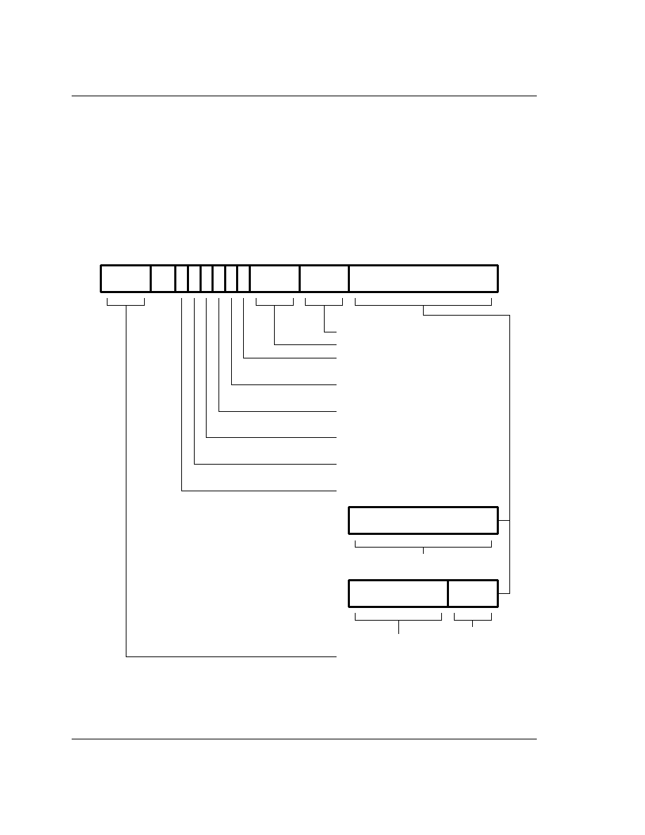
P60ARM-B
36
4.7 Single data transfer (LDR, STR)
The instruction is only executed if the condition is true. The various conditions are defined at the beginning
of this chapter. The instruction encoding is shown in Figure 17: Single Data Transfer Instructions.
The single data transfer instructions are used to load or store single bytes or words of data. The memory
address used in the transfer is calculated by adding an offset to or subtracting an offset from a base register.
The result of this calculation may be written back into the base register if `auto-indexing' is required.
Figure 17: Single Data Transfer Instructions
Cond
I
Rn
Rd
0
11
12
15
16
19
20
21
24
25
26
27
28
31
01
P U B W L
Offset
22
23
0
11
Source/Destination register
Base register
Load/Store bit
0 = Store to memory
1 = Load from memory
Write-back bit
Byte/Word bit
0 = no write-back
1 = write address into base
0 = transfer word quantity
1 = transfer byte quantity
Up/Down bit
Pre/Post indexing bit
0 = offset is an immediate value
Immediate offset
Immediate offset
Unsigned 12 bit immediate offset
1 = offset is a register
11
0
shift applied to Rm
3
4
Condition field
0 = down; subtract offset from base
1 = up; add offset to base
0 = post; add offset after transfer
1 = pre; add offset before transfer
Offset register
Shift
Rm

Instruction Set - LDR, STR
37
4.7.1 Offsets and auto-indexing
The offset from the base may be either a 12 bit unsigned binary immediate value in the instruction, or a
second register (possibly shifted in some way). The offset may be added to (U=1) or subtracted from (U=0)
the base register Rn. The offset modification may be performed either before (pre-indexed, P=1) or after
(post-indexed, P=0) the base is used as the transfer address.
The W bit gives optional auto increment and decrement addressing modes. The modified base value may
be written back into the base (W=1), or the old base value may be kept (W=0). In the case of post-indexed
addressing, the write back bit is redundant and is always set to zero, since the old base value can be retained
by setting the offset to zero. Therefore post-indexed data transfers always write back the modified base. The
only use of the W bit in a post-indexed data transfer is in privileged mode code, where setting the W bit
forces non-privileged mode for the transfer, allowing the operating system to generate a user address in a
system where the memory management hardware makes suitable use of this hardware.
4.7.2 Shifted register offset
The 8 shift control bits are described in the data processing instructions section. However, the register
specified shift amounts are not available in this instruction class. See 4.4.2 Shifts.
4.7.3 Bytes and words
This instruction class may be used to transfer a byte (B=1) or a word (B=0) between an ARM60 register and
memory.
The action of LDR(B) and STR(B) instructions is influenced by the BIGEND control signal. The two possible
configurations are described below.
Little Endian Configuration
A byte load (LDRB) expects the data on data bus inputs 7 through 0 if the supplied address is on a word
boundary, on data bus inputs 15 through 8 if it is a word address plus one byte, and so on. The selected byte
is placed in the bottom 8 bits of the destination register, and the remaining bits of the register are filled with
zeros.
A byte store (STRB) repeats the bottom 8 bits of the source register four times across data bus outputs 31
through 0. The external memory system should activate the appropriate byte subsystem to store the data.
A word load (LDR) will normally use a word aligned address. However, an address offset from a word
boundary will cause the data to be rotated into the register so that the addressed byte occupies bits 0 to 7.
This means that half-words accessed at offsets 0 and 2 from the word boundary will be correctly loaded into
bits 0 through 15 of the register. Two shift operations are then required to clear or to sign extend the upper
16 bits.
A word store (STR) should generate a word aligned address. The word presented to the data bus is not
affected if the address is not word aligned. That is, bit 31 of the register being stored always appears on data
bus output 31.

P60ARM-B
38
Big Endian Configuration
A byte load (LDRB) expects the data on data bus inputs 31 through 24 if the supplied address is on a word
boundary, on data bus inputs 23 through 16 if it is a word address plus one byte, and so on. The selected
byte is placed in the bottom 8 bits of the destination register and the remaining bits of the register are filled
with zeros.
A byte store (STRB) repeats the bottom 8 bits of the source register four times across data bus outputs 31
through 0. The external memory system should activate the appropriate byte subsystem to store the data.
A word load (LDR) should generate a word aligned address. An address offset of 0 or 2 from a word
boundary will cause the data to be rotated into the register so that the addressed byte occupies bits 31
through 24. This means that half-words accessed at these offsets will be correctly loaded into bits 16 through
31 of the register. A shift operation is then required to move (and optionally sign extend) the data into the
bottom 16 bits. An address offset of 1 or 3 from a word boundary will cause the data to be rotated into the
register so that the addressed byte occupies bits 15 through 8.
A word store (STR) should generate a word aligned address. The word presented to the data bus is not
affected if the address is not word aligned. That is, bit 31 of the register being stored always appears on data
bus output 31.
4.7.4 Use of R15
Write-back shall not be specified if R15 is specified as the base register (Rn). When using R15 as the base
register you must remember it contains an address 8 bytes on from the address of the current instruction.
R15 shall not be specified as the register offset (Rm).
When R15 is the source register (Rd) of a register store (STR) instruction, the stored value will be address
of the instruction plus 12.
4.7.5 Restriction on the use of base register
When configured for late aborts, the following example code is difficult to unwind as the base register, Rn,
gets updated before the abort handler starts. Sometimes it may be impossible to calculate the initial value.
For example:
LDR
R0,[R1],R1
<LDR|STR> Rd, [Rn],{+/-}Rn{,<shift>}
Therefore a post-indexed LDR|STR where Rm is the same register as Rn shall not be used.

Instruction Set - LDR, STR
39
4.7.6 Data Aborts
A transfer to or from a legal address may cause problems for a memory management system. For instance,
in a system which uses virtual memory the required data may be absent from main memory. The memory
manager can signal a problem by taking the processor ABORT input HIGH whereupon the Data Abort trap
will be taken. It is up to the system software to resolve the cause of the problem, then the instruction can be
restarted and the original program continued.
ARM60 supports two types of Data Abort processing depending on the LATEABT control signal. When set
for Early Aborts, any base register write-back which would have occurred is prevented in the event of an
abort. When configured for Late Aborts, this write-back is allowed to take place and the Abort handler must
correct this before allowing the instruction to be re-executed.
4.7.7 Instruction Cycle Times
Normal LDR instructions take 1S + 1N + 1I and LDR PC take 2S + 2N +1I incremental cycles, where S,N
and I are as defined in section 5.1 Cycle types on page 65.
STR instructions take 2N incremental cycles to execute.
4.7.8 Assembler syntax
<LDR|STR>{cond}{B}{T} Rd,<Address>
LDR - load from memory into a register
STR - store from a register into memory
{cond} - two-character condition mnemonic, see Figure 6: Condition Codes
{B} - if B is present then byte transfer, otherwise word transfer
{T} - if T is present the W bit will be set in a post-indexed instruction, forcing non-privileged mode for the
transfer cycle. T is not allowed when a pre-indexed addressing mode is specified or implied.
Rd is an expression evaluating to a valid register number.
<Address> can be:
(i)
An expression which generates an address:
<expression>
The assembler will attempt to generate an instruction using the PC as a base and a corrected
immediate offset to address the location given by evaluating the expression. This will be a PC
relative, pre-indexed address. If the address is out of range, an error will be generated.
(ii)
A pre-indexed addressing specification:
[Rn]
offset of zero
[Rn,<#expression>]{!}
offset of <expression> bytes

P60ARM-B
40
[Rn,{+/-}Rm{,<shift>}]{!}
offset of +/- contents of index register, shifted by <shift>
(iii)
A post-indexed addressing specification:
[Rn],<#expression>
offset of <expression> bytes
[Rn],{+/-}Rm{,<shift>}
offset of +/- contents of index register, shifted as by <shift>.
Rn and Rm are expressions evaluating to a register number. If Rn is R15 then the assembler will subtract 8
from the offset value to allow for ARM60 pipelining. In this case base write-back shall not be specified.
<shift> is a general shift operation (see section on data processing instructions) but note that the shift
amount may not be specified by a register.
{!} writes back the base register (set the W bit) if ! is present.
4.7.9 Examples
STR
R1,[R2,R4]!
; store R1 at R2+R4 (both of which are
; registers) and write back address to R2
STR
R1,[R2],R4
; store R1 at R2 and write back
; R2+R4 to R2
LDR
R1,[R2,#16]
; load R1 from contents of R2+16
; Don't write back
LDR
R1,[R2,R3,LSL#2]
; load R1 from contents of R2+R3*4
LDREQB
R1,[R6,#5]
; conditionally load byte at R6+5 into
; R1 bits 0 to 7, filling bits 8 to 31
; with zeros
STR
R1,PLACE
; generate PC relative offset to address
�
; PLACE
�
PLACE

Instruction Set - LDM, STM
41
4.8 Block data transfer (LDM, STM)
The instruction is only executed if the condition is true. The various conditions are defined at the beginning
of this chapter. The instruction encoding is shown in Figure 18: Block Data Transfer Instructions.
Block data transfer instructions are used to load (LDM) or store (STM) any subset of the currently visible
registers. They support all possible stacking modes, maintaining full or empty stacks which can grow up or
down memory, and are very efficient instructions for saving or restoring context, or for moving large blocks
of data around main memory.
4.8.1 The register list
The instruction can cause the transfer of any registers in the current bank (and non-user mode programs
can also transfer to and from the user bank, see below). The register list is a 16 bit field in the instruction,
with each bit corresponding to a register. A 1 in bit 0 of the register field will cause R0 to be transferred, a
0 will cause it not to be transferred; similarly bit 1 controls the transfer of R1, and so on.
Any subset of the registers, or all the registers, may be specified. The only restriction is that the register list
should not be empty.
Whenever R15 is stored to memory the stored value is the address of the STM instruction plus 12.
Figure 18: Block Data Transfer Instructions
4.8.2 Addressing modes
The transfer addresses are determined by the contents of the base register (Rn), the pre/post bit (P) and the
up/down bit (U). The registers are transferred in the order lowest to highest, so R15 (if in the list) will
always be transferred last. The lowest register also gets transferred to/from the lowest memory address. By
way of illustration, consider the transfer of R1, R5 and R7 in the case where Rn=0x1000 and write back of
Cond
Rn
0
15
16
19
20
21
24
25
27
28
31
P U
W L
22
23
100
S
Register list
Base register
Load/Store bit
0 = Store to memory
1 = Load from memory
Write-back bit
0 = no write-back
1 = write address into base
Up/Down bit
Pre/Post indexing bit
0 = down; subtract offset from base
1 = up; add offset to base
0 = post; add offset after transfer
1 = pre; add offset before transfer
PSR & force user bit
0 = do not load PSR or force user mode
1 = load PSR or force user mode
Condition field

P60ARM-B
42
the modified base is required (W=1). Figure 19: Post-increment addressing, Figure 20: Pre-increment addressing,
Figure 21: Post-decrement addressing and Figure 22: Pre-decrement addressing show the sequence of register
transfers, the addresses used, and the value of Rn after the instruction has completed.
In all cases, had write back of the modified base not been required (W=0), Rn would have retained its initial
value of 0x1000 unless it was also in the transfer list of a load multiple register instruction, when it would
have been overwritten with the loaded value.
4.8.3 Address Alignment
The address should normally be a word aligned quantity and non-word aligned addresses do not affect the
instruction. However, the bottom 2 bits of the address will appear on A[1:0] and might be interpreted by
the memory system.
Figure 19: Post-increment addressing
0x100C
0x1000
0x0FF4
Rn
1
0x100C
0x1000
0x0FF4
2
R1
0x100C
0x1000
0x0FF4
3
0x100C
0x1000
0x0FF4
4
R1
R7
R5
R1
R5
Rn

Instruction Set - LDM, STM
43
Figure 20: Pre-increment addressing
Figure 21: Post-decrement addressing
0x100C
0x1000
0x0FF4
Rn
1
0x100C
0x1000
0x0FF4
2
R1
0x100C
0x1000
0x0FF4
3
0x100C
0x1000
0x0FF4
4
R1
R7
R5
R1
R5
Rn
0x100C
0x1000
0x0FF4
Rn
1
0x100C
0x1000
0x0FF4
2
R1
0x100C
0x1000
0x0FF4
3
0x100C
0x1000
0x0FF4
4
R1
R7
R5
R1
R5
Rn
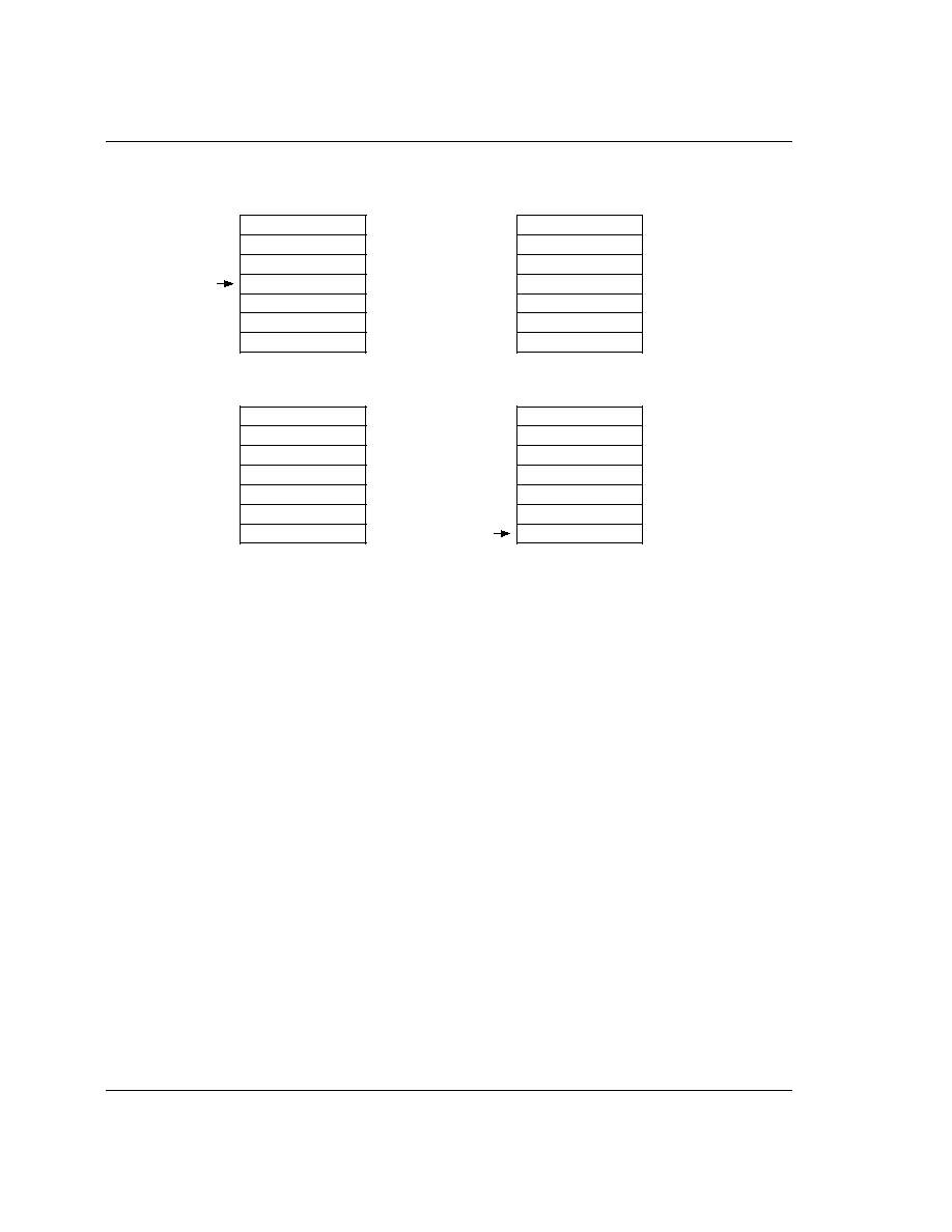
P60ARM-B
44
Figure 22: Pre-decrement addressing
4.8.4 Use of the S bit
When the S bit is set in a LDM/STM instruction its meaning depends on whether or not R15 is in the transfer
list and on the type of instruction. The S bit should only be set if the instruction is to execute in a privileged
mode.
LDM with R15 in transfer list and S bit set (Mode changes)
If the instruction is a LDM then SPSR_<mode> is transferred to CPSR at the same time as R15 is loaded.
STM with R15 in transfer list and S bit set (User bank transfer)
The registers transferred are taken from the User bank rather than the bank corresponding to the current
mode. This is useful for saving the user state on process switches. Base write-back shall not be used when
this mechanism is employed.
R15 not in list and S bit set (User bank transfer)
For both LDM and STM instructions, the User bank registers are transferred rather than the register bank
corresponding to the current mode. This is useful for saving the user state on process switches. Base write-
back shall not be used when this mechanism is employed.
When the instruction is LDM, care must be taken not to read from a banked register during the following
cycle (inserting a NOP after the LDM will ensure safety).
0x100C
0x1000
0x0FF4
Rn
1
0x100C
0x1000
0x0FF4
2
R1
0x100C
0x1000
0x0FF4
3
0x100C
0x1000
0x0FF4
4
R1
R7
R5
R1
R5
Rn

Instruction Set - LDM, STM
45
4.8.5 Use of R15 as the base
R15 shall not be used as the base register in any LDM or STM instruction.
4.8.6 Inclusion of the base in the register list
When write-back is specified, the base is written back at the end of the second cycle of the instruction.
During a STM, the first register is written out at the start of the second cycle. A STM which includes storing
the base, with the base as the first register to be stored, will therefore store the unchanged value, whereas
with the base second or later in the transfer order, will store the modified value. A LDM will always
overwrite the updated base if the base is in the list.
4.8.7 Data Aborts
Some legal addresses may be unacceptable to a memory management system, and the memory manager
can indicate a problem with an address by taking the ABORT signal HIGH. This can happen on any
transfer during a multiple register load or store, and must be recoverable if ARM60 is to be used in a virtual
memory system.
The state of the LATEABT control signal does not affect the behaviour of LDM and STM instructions in the
event of a memory abort exception.
Aborts during STM instructions
If the abort occurs during a store multiple instruction, ARM60 takes little action until the instruction
completes, whereupon it enters the data abort trap. The memory manager is responsible for preventing
erroneous writes to the memory. The only change to the internal state of the processor will be the
modification of the base register if write-back was specified, and this must be reversed by software (and the
cause of the abort resolved) before the instruction may be retried.
Aborts during LDM instructions
When ARM60 detects a data abort during a load multiple instruction, it modifies the operation of the
instruction to ensure that recovery is possible.
(i)
Overwriting of registers stops when the abort happens. The aborting load will not take place but
earlier ones may have overwritten registers. The PC is always the last register to be written and so
will always be preserved.
(ii)
The base register is restored, to its modified value if write-back was requested. This ensures
recoverability in the case where the base register is also in the transfer list, and may have been
overwritten before the abort occurred.
The data abort trap is taken when the load multiple has completed, and the system software must undo any
base modification (and resolve the cause of the abort) before restarting the instruction.
4.8.8 Instruction Cycle Times
Normal LDM instructions take nS + 1N + 1I and LDM PC takes (n+1)S + 2N + 1I incremental cycles, where
S,N and I are as defined in section 5.1 Cycle types on page 65.

P60ARM-B
46
STM instructions take (n-1)S + 2N incremental cycles to execute.
n
is the number of words transferred.
4.8.9 Assembler syntax
<LDM|STM>{cond}<FD|ED|FA|EA|IA|IB|DA|DB> Rn{!},<Rlist>{^}
{cond} - two character condition mnemonic, see Figure 6: Condition Codes
Rn is an expression evaluating to a valid register number
<Rlist> is a list of registers and register ranges enclosed in {} (eg {R0,R2-R7,R10}).
{!} if present requests write-back (W=1), otherwise W=0
{^} if present set S bit to load the CPSR along with the PC, or force transfer of user bank when in privileged
mode
Addressing mode names
There are different assembler mnemonics for each of the addressing modes, depending on whether the
instruction is being used to support stacks or for other purposes. The equivalences between the names and
the values of the bits in the instruction are shown in the following table:
FD, ED, FA, EA define pre/post indexing and the up/down bit by reference to the form of stack required.
The F and E refer to a �full� or �empty� stack, i.e. whether a pre-index has to be done (full) before storing
to the stack. The A and D refer to whether the stack is ascending or descending. If ascending, a STM will go
up and LDM down, if descending, vice-versa.
name
stack
other
L bit
P bit
U bit
pre-increment load
LDMED
LDMIB
1
1
1
post-increment load
LDMFD
LDMIA
1
0
1
pre-decrement load
LDMEA
LDMDB
1
1
0
post-decrement load
LDMFA
LDMDA
1
0
0
pre-increment store
STMFA
STMIB
0
1
1
post-increment store
STMEA
STMIA
0
0
1
pre-decrement store
STMFD
STMDB
0
1
0
post-decrement store
STMED
STMDA
0
0
0
Table 5:
Addressing Mode Names

Instruction Set - LDM, STM
47
IA, IB, DA, DB allow control when LDM/STM are not being used for stacks and simply mean Increment
After, Increment Before, Decrement After, Decrement Before.
4.8.10 Examples
LDMFD
SP!,{R0,R1,R2}
; unstack 3 registers
STMIA
R0,{R0-R15}
; save all registers
LDMFD
SP!,{R15}
; R15 <- (SP),CPSR unchanged
LDMFD
SP!,{R15}^
; R15 <- (SP), CPSR <- SPSR_mode (allowed
; only in privileged modes)
STMFD
R13,{R0-R14}^
; Save user mode regs on stack (allowed
; only in privileged modes)
These instructions may be used to save state on subroutine entry, and restore it efficiently on return to the
calling routine:
STMED
SP!,{R0-R3,R14}
; save R0 to R3 to use as workspace
; and R14 for returning
BL
somewhere
; this nested call will overwrite R14
LDMED
SP!,{R0-R3,R15}
; restore workspace and return

P60ARM-B
48
4.9 Single data swap (SWP)
The instruction is only executed if the condition is true. The various conditions are defined at the beginning
of this chapter. The instruction encoding is shown in Figure 23: Swap Instruction.
The data swap instruction is used to swap a byte or word quantity between a register and external memory.
This instruction is implemented as a memory read followed by a memory write which are �locked�
together (the processor cannot be interrupted until both operations have completed, and the memory
manager is warned to treat them as inseparable). This class of instruction is particularly useful for
implementing software semaphores. )
Figure 23: Swap Instruction
The swap address is determined by the contents of the base register (Rn). The processor first reads the
contents of the swap address. Then it writes the contents of the source register (Rm) to the swap address,
and stores the old memory contents in the destination register (Rd). The same register may be specified as
both the source and destination.
The LOCK output goes HIGH for the duration of the read and write operations to signal to the external
memory manager that they are locked together, and should be allowed to complete without interruption.
This is important in multi-processor systems where the swap instruction is the only indivisible instruction
which may be used to implement semaphores; control of the memory must not be removed from a
processor while it is performing a locked operation.
4.9.1 Bytes and words
This instruction class may be used to swap a byte (B=1) or a word (B=0) between an ARM60 register and
memory. The SWP instruction is implemented as a LDR followed by a STR and the action of these is as
described in the section on single data transfers. In particular, the description of Big and Little Endian
configuration applies to the SWP instruction.
4.9.2 Use of R15
R15 shall not be used as an operand (Rd, Rn or Rs) in a SWP instruction.
0
11
12
15
16
19
20
27
28
31
23
7
8
4
3
Condition field
Cond
Rn
Rd
1001
0000
Rm
00
B
00010
22 21
Destination register
Source register
Base register
Byte/Word bit
0 = swap word quantity
1 = swap byte quantity

Instruction Set - SWP
49
4.9.3 Data
Aborts
If the address used for the swap is unacceptable to a memory management system, the internal MMU or
external memory manager can flag the problem by driving ABORT HIGH. This can happen on either the
read or the write cycle (or both), and in either case, the Data Abort trap will be taken. It is up to the system
software to resolve the cause of the problem, then the instruction can be restarted and the original program
continued.
Because no base register write-back is allowed, the behaviour of an aborted SWP instruction is the same
regardless of the state of the LATEABT control signal.
4.9.4 Instruction Cycle Times
Swap instructions take 1S + 2N +1I incremental cycles to execute, where S,N and I are as defined in section
5.1 Cycle types on page 65.
4.9.5 Assembler syntax
<SWP>{cond}{B} Rd,Rm,[Rn]
{cond} - two-character condition mnemonic, see Figure 6: Condition Codes
{B} - if B is present then byte transfer, otherwise word transfer
Rd,Rm,Rn are expressions evaluating to valid register numbers
4.9.6 Examples
SWP
R0,R1,[R2]
; load R0 with the contents of R2, and
; store R1 at R2
SWPB
R2,R3,[R4]
; load R2 with the byte at R4, and
; store bits 0 to 7 of R3 at R4
SWPEQ
R0,R0,[R1]
; conditionally swap the contents of R1
; with R0

P60ARM-B
50
4.10 Software interrupt (SWI)
The instruction is only executed if the condition is true. The various conditions are defined at the beginning
of this chapter. The instruction encoding is shown in Figure 24: Software Interrupt Instruction.
The software interrupt instruction is used to enter Supervisor mode in a controlled manner. The instruction
causes the software interrupt trap to be taken, which effects the mode change. The PC is then forced to a
fixed value (0x08) and the CPSR is saved in SPSR_svc. If the SWI vector address is suitably protected (by
external memory management hardware) from modification by the user, a fully protected operating system
may be constructed.
Figure 24: Software Interrupt Instruction
4.10.1 Return from the supervisor
The PC is saved in R14_svc upon entering the software interrupt trap, with the PC adjusted to point to the
word after the SWI instruction. MOVS PC,R14_svc will return to the calling program and restore the CPSR.
Note that the link mechanism is not re-entrant, so if the supervisor code wishes to use software interrupts
within itself it must first save a copy of the return address and SPSR.
4.10.2 Comment �eld
The bottom 24 bits of the instruction are ignored by the processor, and may be used to communicate
information to the supervisor code. For instance, the supervisor may look at this field and use it to index
into an array of entry points for routines which perform the various supervisor functions.
4.10.3 Instruction Cycle Times
Software interrupt instructions take 2S + 1N incremental cycles to execute, where S and N are as defined
in section 5.1 Cycle types on page 65.
4.10.4 Assembler syntax
SWI{cond} <expression>
{cond} - two character condition mnemonic, see Figure 6: Condition Codes
<expression> is evaluated and placed in the comment field (which is ignored by ARM60).
31
28 27
24 23
0
Condition field
1111
Cond
Comment field (ignored by Processor)

Instruction Set - SWI
51
4.10.5 Examples
SWI
ReadC
; get next character from read stream
SWI
WriteI+"k"
; output a "k" to the write stream
SWINE
0
; conditionally call supervisor
; with 0 in comment field
The above examples assume that suitable supervisor code exists, for instance:
0x08 B Supervisor
; SWI entry point
EntryTable
; addresses of supervisor routines
DCD ZeroRtn
DCD ReadCRtn
DCD WriteIRtn
. . .
Zero
EQU 0
ReadC
EQU 256
WriteI
EQU 512
Supervisor
; SWI has routine required in bits 8-23 and data (if any) in bits 0-7.
; Assumes R13_svc points to a suitable stack
STMFD
R13,{R0-R2,R14}
; save work registers and return address
LDR
R0,[R14,#-4]
; get SWI instruction
BIC
R0,R0,#0xFF000000
; clear top 8 bits
MOV
R1,R0,LSR#8
; get routine offset
ADR
R2,EntryTable
; get start address of entry table
LDR
R15,[R2,R1,LSL#2]
; branch to appropriate routine
WriteIRtn
; enter with character in R0 bits 0-7
. . . . . .
LDMFD
R13,{R0-R2,R15}^
; restore workspace and return
; restoring processor mode and flags
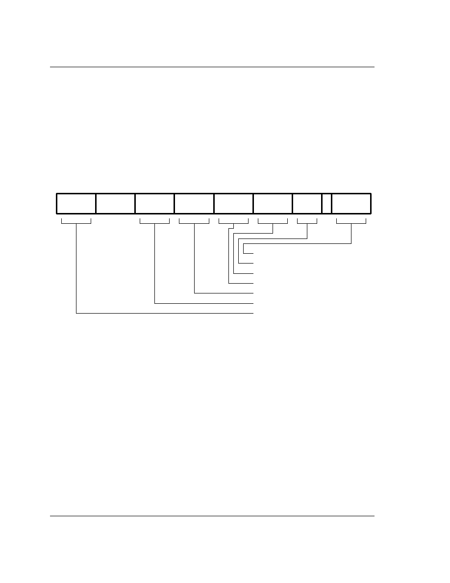
P60ARM-B
52
4.11 Coprocessor data operations (CDP)
The instruction is only executed if the condition is true. The various conditions are defined at the beginning
of this chapter. The instruction encoding is shown in Figure 25: Coprocessor Data Operation Instruction.
This class of instruction is used to tell a coprocessor to perform some internal operation. No result is
communicated back to ARM60, and it will not wait for the operation to complete. The coprocessor could
contain a queue of such instructions awaiting execution, and their execution can overlap other ARM60
activity allowing the coprocessor and ARM60 to perform independent tasks in parallel.
Figure 25: Coprocessor Data Operation Instruction
4.11.1 The Coprocessor �elds
Only bit 4 and bits 24 to 31 are significant to ARM60; the remaining bits are used by coprocessors. The above
field names are used by convention, and particular coprocessors may redefine the use of all fields except
CP# as appropriate. The CP# field is used to contain an identifying number (in the range 0 to 15) for each
coprocessor, and a coprocessor will ignore any instruction which does not contain its number in the CP#
field.
The conventional interpretation of the instruction is that the coprocessor should perform an operation
specified in the CP Opc field (and possibly in the CP field) on the contents of CRn and CRm, and place the
result in CRd.
4.11.2 Instruction Cycle Times
Coprocessor data operations take 1S + bI incremental cycles to execute, where S and I are as defined in
section 5.1 Cycle types on page 65.
b
is the number of cycles spent in the coprocessor busy-wait loop.
Cond
0
11
12
15
16
19
20
24
27
28
31
23
CRd
CP#
7
8
1110
CP Opc
CRn
CP
0
CRm
5
4
3
Coprocessor number
Condition field
Coprocessor information
Coprocessor operand register
Coprocessor destination register
Coprocessor operand register
Coprocessor operation code

Instruction Set - CDP
53
4.11.3 Assembler syntax
CDP{cond} p#,<expression1>,cd,cn,cm{,<expression2>}
{cond} - two character condition mnemonic, see Figure 6: Condition Codes
p# - the unique number of the required coprocessor
<expression1> - evaluated to a constant and placed in the CP Opc field
cd, cn and cm evaluate to the valid coprocessor register numbers CRd, CRn and CRm respectively
<expression2> - where present is evaluated to a constant and placed in the CP field
4.11.4 Examples
CDP
p1,10,c1,c2,c3
; request coproc 1 to do operation 10
; on CR2 and CR3, and put the result in CR1
CDPEQ
p2,5,c1,c2,c3,2
; if Z flag is set request coproc 2 to do
; operation 5 (type 2) on CR2 and CR3,
; and put the result in CR1
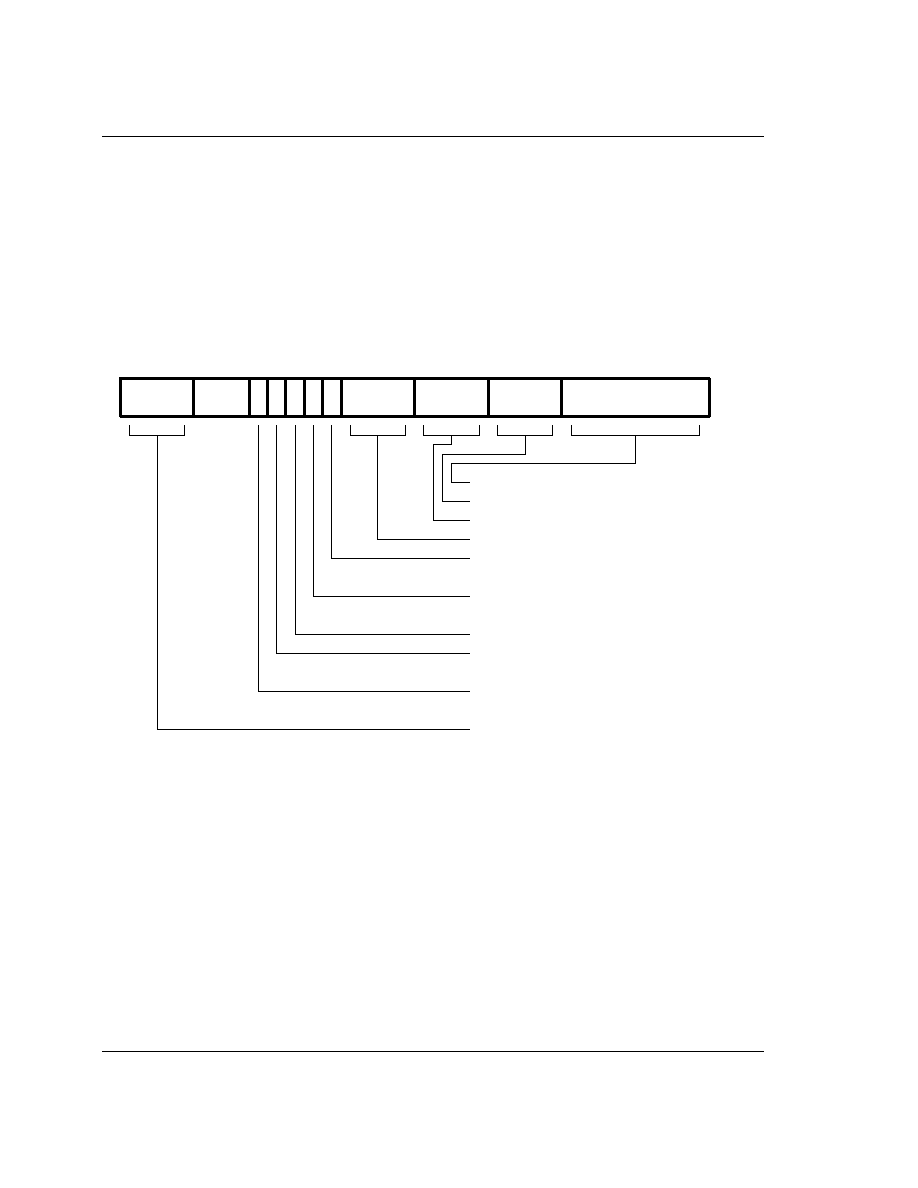
P60ARM-B
54
4.12 Coprocessor data
transfers (LDC, STC)
The instruction is only executed if the condition is true. The various conditions are defined at the beginning
of this chapter. The instruction encoding is shown in Figure 26: Coprocessor Data Transfer Instructions.
This class of instruction is used to load (LDC) or store (STC) a subset of a coprocessors�s registers directly
to memory. ARM60 is responsible for supplying the memory address, and the coprocessor supplies or
accepts the data and controls the number of words transferred.
Figure 26: Coprocessor Data Transfer Instructions
4.12.1 The Coprocessor �elds
The CP# field is used to identify the coprocessor which is required to supply or accept the data, and a
coprocessor will only respond if its number matches the contents of this field.
The CRd field and the N bit contain information for the coprocessor which may be interpreted in different
ways by different coprocessors, but by convention CRd is the register to be transferred (or the first register
where more than one is to be transferred), and the N bit is used to choose one of two transfer length options.
For instance N=0 could select the transfer of a single register, and N=1 could select the transfer of all the
registers for context switching.
Cond
Rn
0
11
12
15
16
19
20
21
24
25
27
28
31
P U
W L
22
23
110
N
CRd
CP#
Offset
7
8
Coprocessor number
Unsigned 8 bit immediate offset
Base register
Load/Store bit
0 = Store to memory
1 = Load from memory
Write-back bit
0 = no write-back
1 = write address into base
Coprocessor source/destination register
Pre/Post indexing bit
Up/Down bit
0 = down; subtract offset from base
1 = up; add offset to base
0 = post; add offset after transfer
Transfer length
Condition field
1 = pre; add offset before transfer

Instruction Set - LDC, STC
55
4.12.2 Addressing modes
ARM60 is responsible for providing the address used by the memory system for the transfer, and the
addressing modes available are a subset of those used in single data transfer instructions. Note, however,
that the immediate offsets are 8 bits wide and specify word offsets for coprocessor data transfers, whereas
they are 12 bits wide and specify byte offsets for single data transfers.
The 8 bit unsigned immediate offset is shifted left 2 bits and either added to (U=1) or subtracted from (U=0)
the base register (Rn); this calculation may be performed either before (P=1) or after (P=0) the base is used
as the transfer address. The modified base value may be overwritten back into the base register (if W=1), or
the old value of the base may be preserved (W=0). Note that post-indexed addressing modes require
explicit setting of the W bit, unlike LDR and STR which always write-back when post-indexed.
The value of the base register, modified by the offset in a pre-indexed instruction, is used as the address for
the transfer of the first word. The second word (if more than one is transferred) will go to or come from an
address one word (4 bytes) higher than the first transfer, and the address will be incremented by one word
for each subsequent transfer.
4.12.3 Address Alignment
The base address should normally be a word aligned quantity. The bottom 2 bits of the address will appear
on A[1:0] and might be interpreted by the memory system.
4.12.4 Use of R15
If Rn is R15, the value used will be the address of the instruction plus 8 bytes. Base write-back to R15 shall
not be specified.
4.12.5 Data aborts
If the address is legal but the memory manager generates an abort, the data trap will be taken. The write-
back of the modified base will take place, but all other processor state will be preserved. The coprocessor is
partly responsible for ensuring that the data transfer can be restarted after the cause of the abort has been
resolved, and must ensure that any subsequent actions it undertakes can be repeated when the instruction
is retried.
The state of the LATEABT control signal does not affect the behaviour of LDC and STC instructions in the
event of an Abort exception.
4.12.6 Instruction Cycle Times
Coprocessor data transfer instructions take (n-1)S + 2N + bI incremental cycles to execute, where S, N and
I are as defined in section 5.1 Cycle types on page 65.
n
is the number of words transferred.
b
is the number of cycles spent in the coprocessor busy-wait loop.
4.12.7 Assembler syntax
<LDC|STC>{cond}{L} p#,cd,<Address>

P60ARM-B
56
LDC - load from memory to coprocessor
STC - store from coprocessor to memory
{L} - when present perform long transfer (N=1), otherwise perform short transfer (N=0)
{cond} - two character condition mnemonic, see Figure 6: Condition Codes
p# - the unique number of the required coprocessor
cd is an expression evaluating to a valid coprocessor register number that is placed in the CRd field
<Address> can be:
(i)
An expression which generates an address:
<expression>
The assembler will attempt to generate an instruction using the PC as a base and a corrected
immediate offset to address the location given by evaluating the expression. This will be a PC
relative, pre-indexed address. If the address is out of range, an error will be generated.
(ii)
A pre-indexed addressing specification:
[Rn]
offset of zero
[Rn,<#expression>]{!}
offset of <expression> bytes
(iii)
A post-indexed addressing specification:
[Rn],<#expression>
offset of <expression> bytes
Rn is an expression evaluating to a valid ARM60 register number. Note, if Rn is R15 then the assembler will
subtract 8 from the offset value to allow for ARM60 pipelining.
{!} write back the base register (set the W bit) if ! is present
4.12.8 Examples
LDC
p1,c2,table
; load c2 of coproc 1 from address table,
; using a PC relative address.
STCEQL
p2,c3,[R5,#24]!
; conditionally store c3 of coproc 2 into
; an address 24 bytes up from R5, write this
; address back to R5, and use long transfer
; option (probably to store multiple words)
Note that though the address offset is expressed in bytes, the instruction offset field is in words. The
assembler will adjust the offset appropriately.
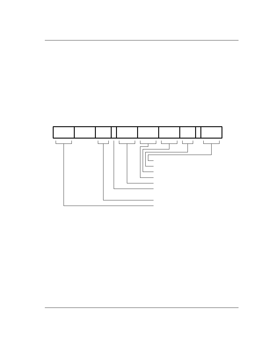
Instruction Set - MRC, MCR
57
4.13 Coprocessor register transfers (MRC, MCR)
The is only executed if the condition is true. The various conditions are defined at the beginning of this
chapter. The instruction encoding is shown in Figure 27: Coprocessor Register Transfer Instructions.
This class of instruction is used to communicate information directly between ARM60 and a coprocessor.
An example of a coprocessor to ARM60 register transfer (MRC) instruction would be a FIX of a floating
point value held in a coprocessor, where the floating point number is converted into a 32 bit integer within
the coprocessor, and the result is then transferred to an ARM60 register. A FLOAT of a 32 bit value in an
ARM60 register into a floating point value within the coprocessor illustrates the use of an ARM60 register
to coprocessor transfer (MCR).
Figure 27: Coprocessor Register Transfer Instructions
An important use of this instruction is to communicate control information directly from the coprocessor
into the ARM60 CPSR flags. As an example, the result of a comparison of two floating point values within
a coprocessor can be moved to the CPSR to control the subsequent flow of execution.
Note for future compatbility the ARM610 has an internal coprocessor (#15) for control of on-chip functions.
Accesses to this coprocessor are performed during coprocessor register transfers.
4.13.1 The Coprocessor �elds
The CP# field is used, as for all coprocessor instructions, to specify which coprocessor is being called upon.
The CP Opc, CRn, CP and CRm fields are used only by the coprocessor, and the interpretation presented
here is derived from convention only. Other interpretations are allowed where the coprocessor
functionality is incompatible with this one. The conventional interpretation is that the CP Opc and CP fields
21
Cond
0
11
12
15
16
19
20
24
27
28
31
23
CP#
7
8
1110
CRn
CP
CRm
5
4
3
1
L
CP Opc
Rd
Coprocessor number
Coprocessor information
Coprocessor operand register
Coprocessor operation mode
Condition field
Load/Store bit
0 = Store to Co-Processor
1 = Load from Co-Processor
ARM source/destination register
Coprocessor source/destination register

P60ARM-B
58
specify the operation the coprocessor is required to perform, CRn is the coprocessor register which is the
source or destination of the transferred information, and CRm is a second coprocessor register which may
be involved in some way which depends on the particular operation specified.
4.13.2 Transfers to R15
When a coprocessor register transfer to ARM60 has R15 as the destination, bits 31, 30, 29 and 28 of the
transferred word are copied into the N, Z, C and V flags respectively. The other bits of the transferred word
are ignored, and the PC and other CPSR bits are unaffected by the transfer.
4.13.3 Transfers from R15
A coprocessor register transfer from ARM60 with R15 as the source register will store the PC+12.
4.13.4 Instruction Cycle Times
MRC instructions take 1S + bI +1C incremental cycles to execute, where S, I and C are as defined in section
5.1 Cycle types on page 65.
MCR instructions take 1S + (b+1)I +1C incremental cycles to execute.
b
is the number of cycles spent in the coprocessor busy-wait loop.
4.13.5 Assembler syntax
<MCR|MRC>{cond} p#,<expression1>,Rd,cn,cm{,<expression2>}
MRC - move from coprocessor to ARM60 register (L=1)
MCR - move from ARM60 register to coprocessor (L=0)
{cond} - two character condition mnemonic, see Figure 6: Condition Codes
p# - the unique number of the required coprocessor
<expression1> - evaluated to a constant and placed in the CP Opc field
Rd is an expression evaluating to a valid ARM60 register number
cn and cm are expressions evaluating to the valid coprocessor register numbers CRn and CRm respectively
<expression2> - where present is evaluated to a constant and placed in the CP field
4.13.6 Examples
MRC
2,5,R3,c5,c6
; request coproc 2 to perform operation 5
; on c5 and c6, and transfer the (single
; 32 bit word) result back to R3
MCR
6,0,R4,c6
; request coproc 6 to perform operation 0
; on R4 and place the result in c6

Instruction Set - MRC, MCR
59
MRCEQ
3,9,R3,c5,c6,2
; conditionally request coproc 3 to perform
; operation 9 (type 2) on c5 and c6, and
; transfer the result back to R3

P60ARM-B
60
4.14 Unde�ned instruction
The instruction is only executed if the condition is true. The various conditions are defined at the beginning
of this chapter. The instruction format is shown in Figure 28: Undefined Instruction.
If the condition is true, the undefined instruction trap will be taken.
Figure 28: Undefined Instruction
Note that the undefined instruction mechanism involves offering this instruction to any coprocessors which
may be present, and all coprocessors must refuse to accept it by driving CPA and CPB HIGH. For systems
without a coprocessor, CPA and CPB must be driven HIGH at all times.
4.14.1 Assembler syntax
At present the assembler has no mnemonics for generating this instruction. If it is adopted in the future for
some specified use, suitable mnemonics will be added to the assembler. Until such time, this instruction
shall not be used.
Cond
0
24
27
28
31
5
4
3
1
011
xxxx
25
xxxxxxxxxxxxxxxxxxxx

Instruction Set - Examples
61
4.15 Instruction Set Examples
The following examples show ways in which the basic ARM60 instructions can combine to give efficient
code. None of these methods saves a great deal of execution time (although they may save some), mostly
they just save code.
4.15.1 Using the conditional instructions
(1)
using conditionals for logical OR
CMP
Rn,#p
; if Rn=p OR Rm=q THEN GOTO Label
BEQ
Label
CMP
Rm,#q
BEQ
Label
can be replaced by
CMP
Rn,#p
CMPNE
Rm,#q
; if condition not satisfied try other test
BEQ
Label
(2)
absolute value
TEQ
Rn,#0
; test sign
RSBMI
Rn,Rn,#0
; and 2's complement if necessary
(3)
multiplication by 4, 5 or 6 (run time)
MOV
Rc,Ra,LSL#2
; multiply by 4
CMP
Rb,#5
; test value
ADDCS
Rc,Rc,Ra
; complete multiply by 5
ADDHI
Rc,Rc,Ra
; complete multiply by 6
(4)
combining discrete and range tests
TEQ
Rc,#127
; discrete test
CMPNE
Rc,#" "-1
; range test
MOVLS
Rc,#"."
; IF Rc<=" " OR Rc=ASCII(127)
; THEN Rc:="."
(5)
division and remainder
; enter with numbers in Ra and Rb
;
MOV
Rcnt,#1
; bit to control the division
Div1
CMP
Rb,#0x80000000
; move Rb until greater than Ra
CMPCC
Rb,Ra
MOVCC
Rb,Rb,ASL#1
MOVCC
Rcnt,Rcnt,ASL#1

P60ARM-B
62
BCC
Div1
MOV
Rc,#0
Div2
CMP
Ra,Rb
; test for possible subtraction
SUBCS
Ra,Ra,Rb
; subtract if ok
ADDCS
Rc,Rc,Rcnt
; put relevant bit into result
MOVS
Rcnt,Rcnt,LSR#1
; shift control bit
MOVNE
Rb,Rb,LSR#1
; halve unless finished
BNE
Div2
;
; divide result in Rc
; remainder in Ra
4.15.2 Pseudo random binary sequence generator
It is often necessary to generate (pseudo-) random numbers and the most efficient algorithms are based on
shift generators with exclusive-OR feedback rather like a cyclic redundancy check generator. Unfortunately
the sequence of a 32 bit generator needs more than one feedback tap to be maximal length (i.e. 2^32-1 cycles
before repetition), so this example uses a 33 bit register with taps at bits 33 and 20. The basic algorithm is
newbit:=bit 33 eor bit 20, shift left the 33 bit number and put in newbit at the bottom; this operation is
performed for all the newbits needed (i.e. 32 bits). The entire operation can be done in 5 S cycles:
; enter with seed in Ra (32 bits),
Rb (1 bit in Rb lsb), uses Rc
;
TST
Rb,Rb,LSR#1
; top bit into carry
MOVS
Rc,Ra,RRX
; 33 bit rotate right
ADC
Rb,Rb,Rb
; carry into lsb of Rb
EOR
Rc,Rc,Ra,LSL#12
; (involved!)
EOR
Ra,Rc,Rc,LSR#20
; (similarly involved!)
;
; new seed in Ra, Rb as before
4.15.3 Multiplication by constant using the barrel shifter
(1)
Multiplication by 2^n (1,2,4,8,16,32..)
MOV
Ra, Rb, LSL #n
(2)
Multiplication by 2^n+1 (3,5,9,17..)
ADD
Ra,Ra,Ra,LSL #n
(3)
Multiplication by 2^n-1 (3,7,15..)
RSB
Ra,Ra,Ra,LSL #n

Instruction Set - Examples
63
(4)
Multiplication by 6
ADD
Ra,Ra,Ra,LSL #1
; multiply by 3
MOV
Ra,Ra,LSL#1
; and then by 2
(5)
Multiply by 10 and add in extra number
ADD
Ra,Ra,Ra,LSL#2
; multiply by 5
ADD
Ra,Rc,Ra,LSL#1
; multiply by 2 and add in next digit
(6)
General recursive method for Rb := Ra*C, C a constant:
(a)
If C even, say C = 2^n*D, D odd:
D=1:
MOV Rb,Ra,LSL #n
D<>1:
{Rb := Ra*D}
MOV
Rb,Rb,LSL #n
(b)
If C MOD 4 = 1, say C = 2^n*D+1, D odd, n>1:
D=1:
ADD Rb,Ra,Ra,LSL #n
D<>1:
{Rb := Ra*D}
ADD
Rb,Ra,Rb,LSL #n
(c)
If C MOD 4 = 3, say C = 2^n*D-1, D odd, n>1:
D=1:
RSB Rb,Ra,Ra,LSL #n
D<>1:
{Rb := Ra*D}
RSB
Rb,Ra,Rb,LSL #n
This is not quite optimal, but close. An example of its non-optimality is multiply by 45 which is done by:
RSB
Rb,Ra,Ra,LSL#2
; multiply by 3
RSB
Rb,Ra,Rb,LSL#2
; multiply by 4*3-1 = 11
ADD
Rb,Ra,Rb,LSL# 2
; multiply by 4*11+1 = 45
rather than by:
ADD
Rb,Ra,Ra,LSL#3
; multiply by 9
ADD
Rb,Rb,Rb,LSL#2
; multiply by 5*9 = 45

P60ARM-B
64
4.15.4 Loading a word from an unknown alignment
; enter with address in Ra (32 bits)
; uses Rb, Rc; result in Rd.
; Note d must be less than c e.g. 0,1
;
BIC
Rb,Ra,#3
; get word aligned address
LDMIA
Rb,{Rd,Rc}
; get 64 bits containing answer
AND
Rb,Ra,#3
; correction factor in bytes
MOVS
Rb,Rb,LSL#3
; ...now in bits and test if aligned
MOVNE
Rd,Rd,LSR Rb
; produce bottom of result word
; (if not aligned)
RSBNE
Rb,Rb,#32
; get other shift amount
ORRNE
Rd,Rd,Rc,LSL Rb
; combine two halves to get result
4.15.5 Loading a halfword (Little Endian)
LDR
Ra, [Rb,#2]
; Get halfword to bits 15:0
MOV
Ra,Ra,LSL #16
; move to top
MOV
Ra,Ra,LSR #16
; and back to bottom
; use ASR to get sign extended version
4.15.6 Loading a halfword (Big Endian)
LDR
Ra, [Rb,#2]
; Get halfword to bits 31:16
MOV
Ra,Ra,LSR #16
; and back to bottom
; use ASR to get sign extended version
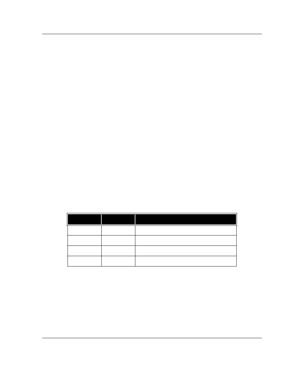
Memory Interface
65
5.0 Memory Interface
ARM60 communicates with its memory system via a bidirectional data bus (
D[31:0]
). A separate 32 bit
address bus specifies the memory location to be used for the transfer, and the
nRW
signal gives the
direction of transfer (ARM60 to memory or memory to ARM60). Control signals give additional
information about the transfer cycle, and in particular they facilitate the use of DRAM page mode where
applicable. Interfaces to static RAM based memories can also be interfaced to and, in general, they are much
simpler than the DRAM interface described here.
5.1 Cycle types
All memory transfer cycles can be placed in one of four categories:
(1)
Non-sequential cycle. ARM60 requests a transfer to or from an address which is unrelated to the
address used in the preceding cycle.
(2)
Sequential cycle. ARM60 requests a transfer to or from an address which is either the same as the
address in the preceding cycle, or is one word after the preceding address.
(3)
Internal cycle. ARM60 does not require a transfer, as it is performing an internal function and no
useful prefetching can be performed at the same time.
(4)
Coprocessor register transfer. ARM60 wishes to use the data bus to communicate with a
coprocessor, but does not require any action by the memory system.
These four classes are distinguishable to the memory system by inspection of the
nMREQ
and
SEQ
control
lines (see
Table 6: Memory Cycle Types
). These control lines are generated during phase 1 of the cycle before
the cycle whose characteristics they forecast, and this pipelining of the control information gives the
memory system sufficient time to decide whether or not it can use a page mode access.
Figure 29: ARM Memory Cycle Timing
shows the pipelining of the control signals, and suggests how the
DRAM address strobes (
nRAS
and
nCAS
) might be timed to use page mode for S-cycles. Note that the N-
cycle is longer than the other cycles. This is to allow for the DRAM precharge and row access time, and is
not an ARM60 requirement.
nMREQ
SEQ
Cycle type
0
0
Non-sequential cycle (N-cycle)
0
1
Sequential cycle (S-cycle)
1
0
Internal cycle (I-cycle)
1
1
Coprocessor register transfer (C-cycle)
Table 6: Memory Cycle Types
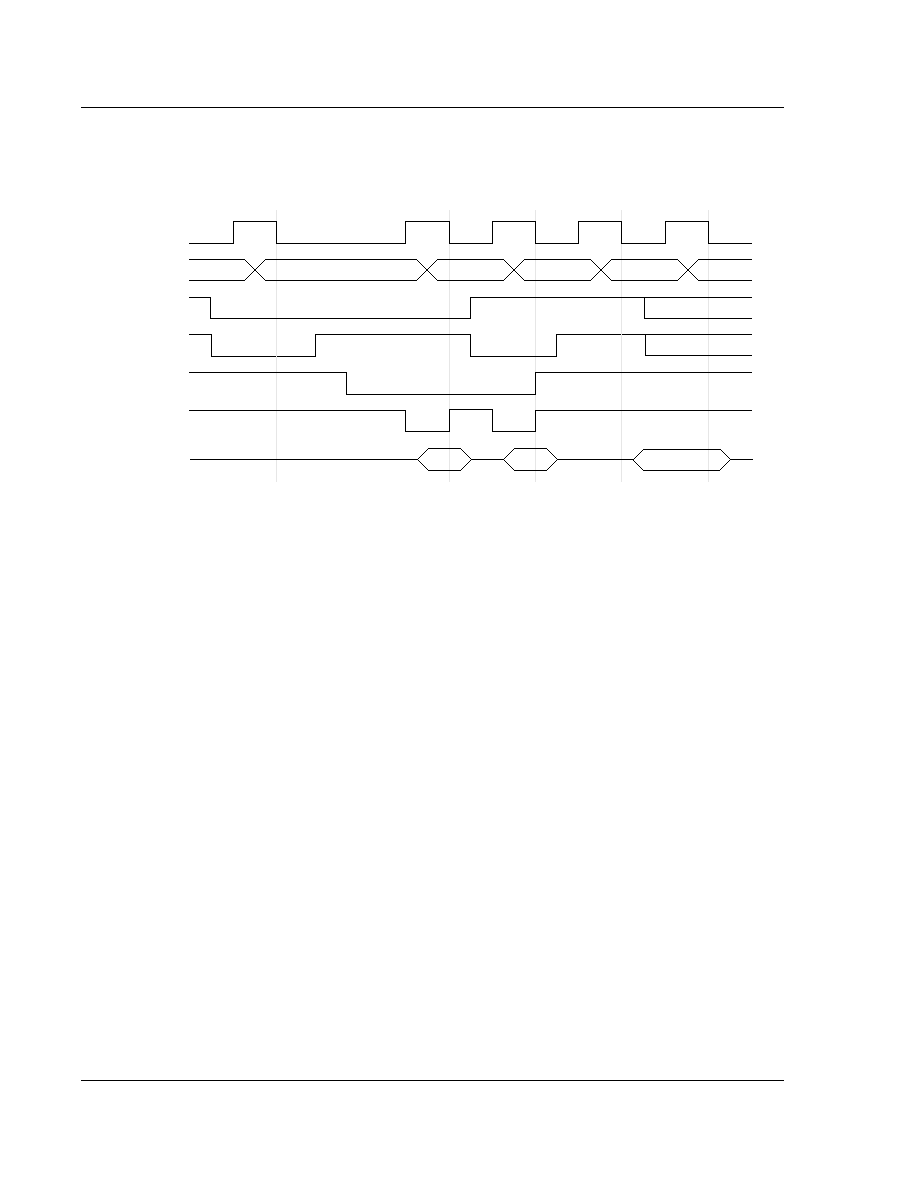
P60ARM-B
66
Figure 29: ARM Memory Cycle Timing
When an S-cycle follows an N-cycle, the address will always be one word greater than the address used in
the N-cycle. This address (marked �a� in the above diagram) should be checked to ensure that it is not the
last in the DRAM page before the memory system commits to the S-cycle. If it is at the page end, the S-cycle
cannot be performed in page mode and the memory system will have to perform a full access.
The processor clock must be stretched to match the full access. When an S-cycle follows an I- or C-cycle, the
address will be the same as that used in the I- or C-cycle. This fact may be used to start the DRAM access
during the preceding cycle, which enables the S-cycle to run at page mode speed whilst performing a full
DRAM access. This is shown in
Figure 30: Memory Cycle Optimization
.
5.2 Byte addressing
The processor address bus gives byte addresses, but instructions are always words (where a word is 4
bytes) and data quantities are usually words. Single data transfers (LDR and STR) can, however, specify
that a byte quantity is required. The
nBW
control line is used to request a byte from the memory system;
normally it is HIGH, signifying a request for a word quantity, and it goes LOW during phase 2 of the
preceding cycle to request a byte transfer.
When the processor is fetching an instruction from memory, the state of the bottom two address lines
A[1:0]
is undefined.
When a byte is requested in a read transfer (LDRB), the memory system can safely ignore that the request
is for a byte quantity and present the whole word.
ARM60 will perform the byte extraction internally. Alternatively, the memory system may activate only the
addressed byte of the memory. This may be desirable in order to save power, or to enable the use of a
common decoding system for both read and write cycles.
MCLK
A[31:0]
nMREQ
SEQ
nCAS
a
a+4
I-cycle
S-cycle
C-cycle
N-cycle
nRAS
D[31:0]
a+8
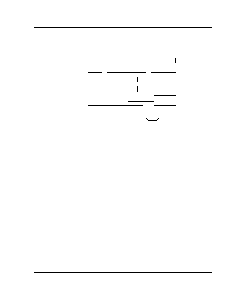
Memory Interface
67
Figure 30: Memory Cycle Optimization
If a byte write is requested (STRB), ARM60
will broadcast the byte value across the data bus, presenting it
at each byte location within the word. The memory system must decode
A[1:0]
to enable writing only to the
addressed byte.
One way of implementing the byte decode in a DRAM system is to separate the 32 bit wide block of DRAM
into four byte wide banks, and generate the column address strobes independently as shown in
Figure 31:
Decoding Byte Accesses to Memory
.
When the processor is configured for Little Endian operation byte 0 of the memory system should be
connected to data lines 7 through 0 (
D[7:0]
) and strobed by
nCAS0
.
nCAS1
drives the bank connected to
data lines 15 though 8, and so on. This has the added advantage of reducing the load on each column strobe
driver, which improves the precision of this time critical signal.
In the Big Endian case, byte 0 of the memory system should be connected to data lines 31 through 24
.
MCLK
A[31:0]
nMREQ
SEQ
nCAS
I-cycle
S-cycle
nRAS
D[31:0]
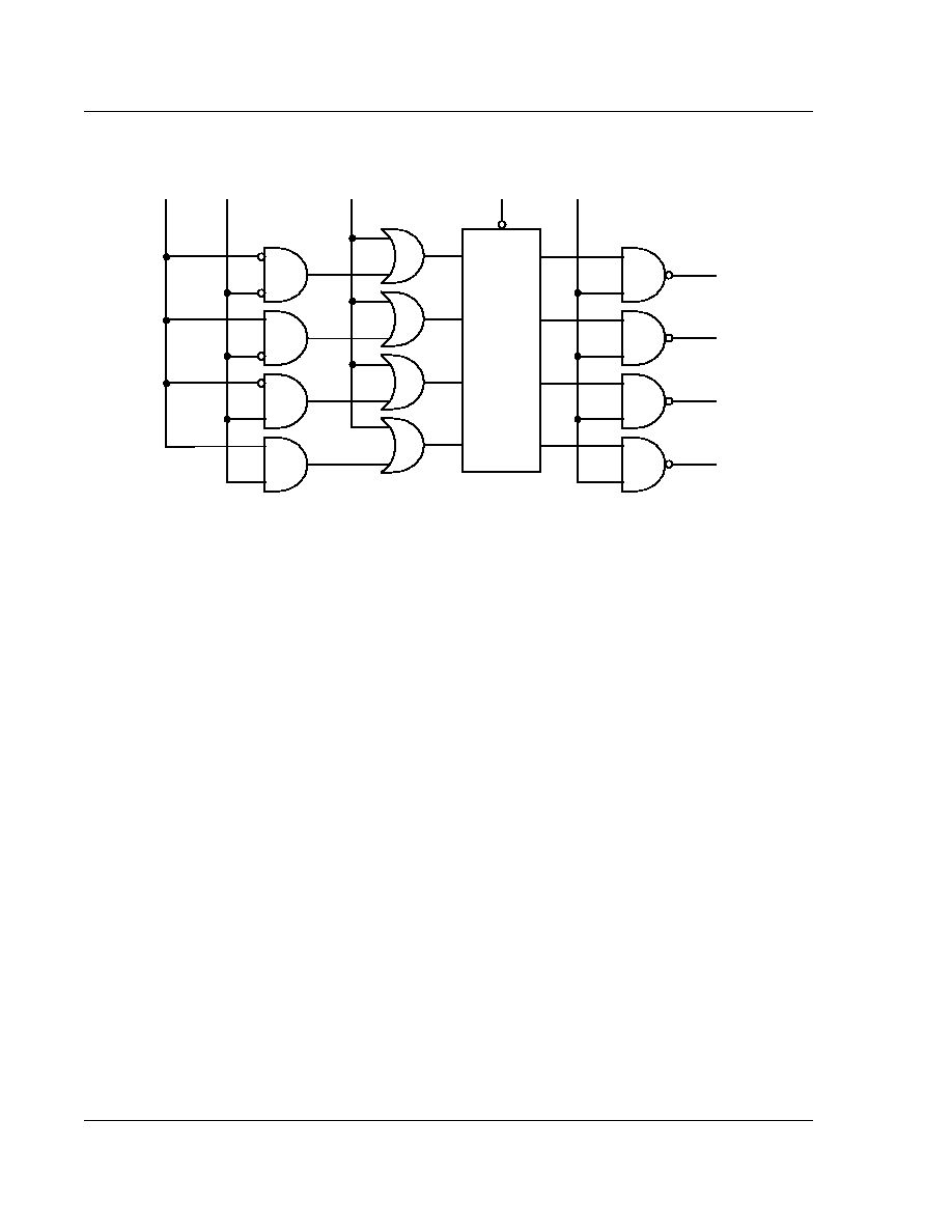
P60ARM-B
68
Figure 31: Decoding Byte Accesses to Memory
5.3 Address timing
Normally the processor address changes during phase 2 to the value which the memory system should use
during the following cycle. This gives maximum time for driving the address to large memory arrays, and
for address translation where required. Dynamic memories usually latch the address on chip, and if the
latch is timed correctly they will work even though the address changes before the access has completed.
Static RAMs and ROMs will not work under such circumstances, as they require the address to be stable
until after the access has completed. Therefore, for use with such devices, the address transition must be
delayed until after the end of phase 2. An on-chip address latch, controlled by
ALE
, allows the address
timing to be modified in this way. In a system with a mixture of static and dynamic memories (which for
these purposes means a mixture of devices with and without address latches), the use of
ALE
may change
dynamically from one cycle to the next, at the discretion of the memory system.
5.4 Memory management
The ARM60 address bus may be processed by an address translation unit before being presented to the
memory, and ARM60 is capable of running a virtual memory system. The abort input to the processor may
be used by the memory manager to inform ARM60 of page faults. Various other signals enable different
page protection levels to be supported:
(1)
nRW
can be used by the memory manager to protect pages from being written to.
(2)
nTRANS
indicates whether the processor is in user or a privileged mode, and may be used to
protect system pages from the user, or to support completely separate mappings for the system and
the user.
A[0]
A[1]
nBW
MCLK
CAS
NCAS0
NCAS1
NCAS2
NCAS3
G
D
Q
Quad
Latch

Memory Interface
69
Address translation will normally only be necessary on an N-cycle, and this fact may be exploited to reduce
power consumption in the memory manager and avoid the translation delay at other times. The times when
translation is necessary can be deduced by keeping track of the cycle types that the processor uses.
If an N-cycle is matched to a full DRAM access, it will be longer than the minimum processor cycle time.
Stretching phase 1 rather than phase 2 will give the translation system more time to generate an
abort
(which must be set up to the end of phase 1).
5.5 Locked operations
ARM60 includes a data swap (SWP) instruction that allows the contents of a memory location to be
swapped with the contents of a processor register. This instruction is implemented as an uninterruptable
pair of accesses; the first access reads the contents of the memory, and the second writes the register data to
the memory. These accesses must be treated as a contiguous operation by the memory controller to prevent
another device from changing the affected memory location before the swap is completed. ARM60 drives
the
LOCK
signal HIGH for the duration of the swap operation to warn the memory controller not to give
the memory to another device.
5.6 Stretching access times
All memory timing is defined by
MCLK
, and long access times can be accommodated by stretching this
clock. It is usual to stretch the LOW period of
MCLK
, as this allows the memory manager to
abort the
operation if the access is eventually unsuccessful (
ABORT
must be setup prior to the rising edge of
MCLK
if
LATEABT
is LOW configuring ARM60 for early aborts).
Either
MCLK
can be stretched before it is applied to ARM60, or the
nWAIT
input can be used together with
a free-running
MCLK
. Taking
nWAIT
LOW has the same effect as stretching the LOW period of
MCLK
,
and
nWAIT
must only change when
MCLK
is LOW.
ARM60 does not contain any dynamic logic which relies upon regular clocking to maintain its internal state.
Therefore there is no limit upon the maximum period for which
MCLK
may be stretched, or
nWAIT
held
LOW.

P60ARM-B
70

Coprocessor Interface
71
6.0 Coprocessor Interface
The functionality of the ARM60 instruction set may be extended by the addition of up to 16 external
coprocessors. When the coprocessor is not present, instructions intended for it will trap, and suitable
software may be installed to emulate its functions. Adding the coprocessor will then increase the system
performance in a software compatible way. Note that some coprocessor numbers have already been
assigned. Contact your supplier for up to date information.
6.1 Interface signals
Three dedicated signals control the coprocessor interface,
nCPI
,
CPA
and
CPB
. The
CPA
and
CPB
inputs
should be driven high except when they are being used for handshaking.
6.1.1 Coprocessor present/absent
ARM60 takes
nCPI
LOW whenever it starts to execute a coprocessor (or undefined) instruction. (This will
not happen if the instruction fails to be executed because of the condition codes.) Each coprocessor will have
a copy of the instruction, and can inspect the CP# field to see which coprocessor it is for. Every coprocessor
in a system must have a unique number and if that number matches the contents of the CP# field the
coprocessor should drive the
CPA
(coprocessor absent) line LOW. If no coprocessor has a number which
matches the CP# field,
CPA
and
CPB
will remain HIGH, and ARM60 will take the undefined instruction
trap. Otherwise ARM60 observes the
CPA
line going LOW, and waits until the coprocessor is not busy.
6.1.2 Busy-waiting
If
CPA
goes LOW, ARM60 will watch the
CPB
(coprocessor busy) line. Only the coprocessor which is
driving
CPA
LOW is allowed to drive
CPB
LOW, and it should do so when it is ready to complete the
instruction. ARM60 will busy-wait while
CPB
is HIGH, unless an enabled interrupt occurs, in which case
it will break off from the coprocessor handshake to process the interrupt. Normally ARM60 will return from
processing the interrupt to retry the coprocessor instruction.
When
CPB
goes LOW, the instruction continues to completion. This will involve data transfers taking place
between the coprocessor and either ARM60 or memory, except in the case of coprocessor data operations
which complete immediately the coprocessor ceases to be busy.
All three interface signals are sampled by both ARM60 and the coprocessor(s) on the rising edge of
MCLK
.
If all three are LOW, the instruction is committed to execution, and if transfers are involved they will start
on the next cycle. If
nCPI
has gone HIGH after being LOW, and before the instruction is committed, ARM60
has broken off from the busy-wait state to service an interrupt. The instruction may be restarted later, but
other coprocessor instructions may come sooner, and the instruction should be discarded.
6.1.3 Pipeline following
In order to respond correctly when a coprocessor instruction arises, each coprocessor must have a copy of
the instruction. All ARM60 instructions are fetched from memory via the main data bus, and coprocessors
are connected to this bus, so they can keep copies of all instructions as they go into the ARM60 pipeline. The
nOPC
signal indicates when an instruction fetch is taking place, and
MCLK
gives the timing of the transfer,
so these may be used together to load an instruction pipeline within the coprocessor.

P60ARM-B
72
6.2 Data transfer cycles
Once the coprocessor has gone not-busy in a data transfer instruction, it must supply or accept data at the
ARM60 bus rate (defined by
MCLK
and
nWAIT
). It can deduce the direction of transfer by inspection of
the L bit in the instruction, but must only drive the bus when permitted to by
DBE
being HIGH. The
coprocessor is responsible for determining the number of words to be transferred; ARM60 will continue to
increment the address by one word per transfer until the coprocessor tells it to stop. The termination
condition is indicated by the coprocessor driving
CPA
and
CPB
HIGH.
There is no limit in principle to the number of words which one coprocessor data transfer can move, but by
convention no coprocessor should allow more than 16 words in one instruction. More than this would
worsen the worst case ARM60 interrupt latency, as the instruction is not interruptible once the transfers
have commenced. At 16 words, this instruction is comparable with a block transfer of 16 registers, and
therefore does not affect the worst case latency.
6.3 Register transfer cycle
The coprocessor register transfer cycle is the one case when ARM60 requires the data bus without requiring
the memory to be active. The memory system is informed that the bus is required by ARM60 taking both
nMREQ
and
SEQ
HIGH. When the bus is free,
DBE
should be taken HIGH to allow ARM60 or the
coprocessor to drive the bus.
6.4 Privileged instructions
The coprocessor may restrict certain instructions for use in privileged modes only. To do this, the
coprocessor will have to track the
nTRANS
output.
As an example of the use of this facility, consider the case of a floating point coprocessor (FPU) in a multi-
tasking system. The operating system could save all the floating point registers on every task switch, but
this is inefficient in a typical system where only one or two tasks will use floating point operations. Instead,
there could be a privileged instruction which turns the FPU on or off. When a task switch happens, the
operating system can turn the FPU off without saving its registers. If the new task attempts an FPU
operation, the FPU will appear to be absent, causing an undefined instruction trap. The operating system
will then realise that the new task requires the FPU, so it will re-enable it and save FPU registers. The task
can then use the FPU as normal. If, however, the new task never attempts an FPU operation (as will be the
case for most tasks), the state saving overhead will have been avoided.
6.5 Idempotency
A consequence of the implementation of the coprocessor interface, with the interruptible busy-wait state, is
that all instructions may be interrupted at any point up to the time when the coprocessor goes not-busy. If
so interrupted, the instruction will normally be restarted from the beginning after the interrupt has been
processed. It is therefore essential that any action taken by the coprocessor before it goes not-busy must be
idempotent, ie must be repeatable with identical results.
For example, consider a FIX operation in a floating point coprocessor which returns the integer result to an
ARM60 register. The coprocessor must stay busy while it performs the floating point to fixed point
conversion, as ARM60 will expect to receive the integer value on the cycle immediately following that

Coprocessor Interface
73
where it goes not-busy. The coprocessor must therefore preserve the original floating point value and not
corrupt it during the conversion, because it will be required again if an interrupt arises during the busy
period.
The coprocessor data operation class of instruction is not generally subject to idempotency considerations,
as the processing activity can take place after the coprocessor goes not-busy. There is no need for ARM60
to be held up until the result is generated, because the result is confined to stay within the coprocessor.
6.6 Unde�ned instructions
Undefined instructions are treated by ARM60 as coprocessor instructions. All coprocessors must be absent
(ie
CPA
and CPB must be HIGH) when an undefined instruction is presented. ARM60 will then take the
undefined instruction trap. Note that the coprocessor need only look at bit 27 of the instruction to
differentiate undefined instructions (which all have 0 in bit 27) from coprocessor instructions (which all
have 1 in bit 27).

P60ARM-B
74
Instruction Cycle Operations
75
7.0 Instruction Cycle Operations
In the following tables nMREQ and SEQ (which are pipelined up to one cycle ahead of the cycle to which
they apply) are shown in the cycle in which they appear, so they predict the type of the next cycle. The
address, nBW, nRW, and nOPC (which appear up to half a cycle ahead) are shown in the cycle to which
they apply.
Key:-
(pc)
=
contents of the pc.
�
=
a varying number
Xn
=
exception vector
7.1 Branch and branch with link
A branch instruction calculates the branch destination in the first cycle, whilst performing a prefetch from
the current PC. This prefetch is done in all cases, since by the time the decision to take the branch has been
reached it is already too late to prevent the prefetch.
During the second cycle a fetch is performed from the branch destination, and the return address is stored
in register 14 if the link bit is set.
The third cycle performs a fetch from the destination + 4, refilling the instruction pipeline, and if the branch
is with link R14 is modified (4 is subtracted from it) to simplify return from SUB PC,R14,#4 to MOV PC,R14.
This makes the STM..{R14} LDM..{PC} type of subroutine work correctly. The cycle timings are shown
below in Table 7: Branch Instruction Cycle Operations
pc is the address of the branch instruction
alu is an address calculated by ARM60
(alu) are the contents of that address, etc
7.2 Data Operations
A data operation executes in a single datapath cycle except where the shift is determined by the contents of
a register. A register is read onto the A bus, and a second register or the immediate field onto the B bus. The
ALU combines the A bus source and the shifted B bus source according to the operation specified in the
instruction, and the result (when required) is written to the destination register. (Compares and tests do not
produce results, only the ALU status flags are affected.)
Cycle
Address
nBW
nRW
Data
nMREQ
SEQ
nOPC
1
pc+8
1
0
(pc + 8)
0
0
0
2
alu
1
0
(alu)
0
1
0
3
alu+4
1
0
(alu + 4)
0
1
0
alu+8
Table 7: Branch Instruction Cycle Operations

P60ARM-B
76
An instruction prefetch occurs at the same time as the above operation, and the program counter is
incremented.
When the shift length is specified by a register, an additional datapath cycle occurs before the above
operation to copy the bottom 8 bits of that register into a holding latch in the barrel shifter. The instruction
prefetch will occur during this first cycle, and the operation cycle will be internal (ie will not request
memory). This internal cycle can be merged with the following sequential access by the memory manager
as the address remains stable through both cycles.
The PC may be one or more of the register operands. When it is the destination external bus activity may
be affected. If the result is written to the PC, the contents of the instruction pipeline are invalidated, and the
address for the next instruction prefetch is taken from the ALU rather than the address incrementer. The
instruction pipeline is refilled before any further execution takes place, and during this time exceptions are
locked out, although will be recorded for subsequent action after the pipeline has been refilled.
PSR Transfer operations exhibit the same timing characteristics as the data operations except that the PC is
never used as a source or destination register. The cycle timings are shown below Table 8: Data Operation
Instruction Cycle Operations.
Cycle
Address
nBW
nRW
Data
nMREQ
SEQ
nOPC
normal
1
pc+8
1
0
(pc+8)
0
1
0
pc+12
dest=pc
1
pc+8
1
0
(pc+8)
0
0
0
2
alu
1
0
(alu)
0
1
0
3
alu+4
1
0
(alu+4)
0
1
0
alu+8
shift(Rs)
1
pc+8
1
0
(pc+8)
1
0
0
2
pc+12
1
0
-
0
1
1
pc+12
shift(Rs)
1
pc+8
1
0
(pc+8)
1
0
0
dest=pc
2
pc+12
1
0
-
0
0
1
3
alu
1
0
(alu)
0
1
0
4
alu+4
1
0
(alu+4)
0
1
0
alu+8
Table 8: Data Operation Instruction Cycle Operations

Instruction Cycle Operations
77
7.3 Multiply and multiply accumulate
The multiply instructions make use of special hardware which implements a 2 bit Booth's algorithm with
early termination. During the first cycle the accumulate Register is brought to the ALU, which either
transmits it or produces zero (depending on the instruction being MLA or MUL) to initialise the destination
register. During the same cycle, the multiplier (Rs) is loaded into the Booth's shifter via the A bus.
The datapath then cycles, adding the multiplicand (Rm) to, subtracting it from, or just transmitting, the
result register. The multiplicand is shifted in the Nth cycle by 2N or 2N+1 bits, under control of the Booth's
logic. The multiplier is shifted right 2 bits per cycle, and when it is zero the instruction terminates (possibly
after an additional cycle to clear a pending borrow).
All cycles except the first are internal. The cycle timings are shown below in Table 9: Multiply Instruction
Cycle Operations.
m is the number of cycles required by the Booth's algorithm; see the section on instruction speeds.
Cycle
Address
nBW
nRW
Data
nMREQ
SEQ
nOPC
(Rs)=0,1
1
pc+8
1
0
(pc+8)
1
0
0
2
pc+12
1
0
-
0
1
1
pc+12
(pc+8)
(Rs)>1
1
pc+8
1
0
(pc+8)
1
0
0
2
pc+12
1
0
-
1
0
1
�
pc+12
1
0
-
1
0
1
m
pc+12
1
0
-
1
0
1
m+1
pc+12
1
0
-
0
1
1
pc+12
Table 9: Multiply Instruction Cycle Operations

P60ARM-B
78
7.4 Load register
The first cycle of a load register instruction performs the address calculation. The data is fetched from
memory during the second cycle, and the base register modification is performed during this cycle (if
required). During the third cycle the data is transferred to the destination register, and external memory is
unused. This third cycle may normally be merged with the following prefetch to form one memory N-cycle.
The cycle timings are shown below in Table 10: Load Register Instruction Cycle Operations.
Either the base or the destination (or both) may be the PC, and the prefetch sequence will be changed if the
PC is affected by the instruction.
The data fetch may abort, and in this case the destination modification is prevented. In addition, if the
processor is configured for Early Abort, the base register write-back is also prevented.
Cycle
Address
nBW
nRW
Data
nMREQ
SEQ
nOPC
normal
1
pc+8
1
0
(pc+8)
0
0
0
2
alu
b/w
0
(alu)
1
0
1
3
pc+12
1
0
-
0
1
1
pc+12
dest=pc
1
pc+8
1
0
(pc+8)
0
0
0
2
alu
b/w
0
pc'
1
0
1
3
pc+12
1
0
-
0
0
1
4
pc'
1
0
(pc')
0
1
0
5
pc'+4
1
0
(pc'+4)
0
1
0
pc'+8
Table 10: Load Register Instruction Cycle Operations
Instruction Cycle Operations
79
7.5 Store register
The first cycle of a store register is similar to the first cycle of load register. During the second cycle the base
modification is performed, and at the same time the data is written to memory. There is no third cycle. The
cycle timings are shown below in Table 11: Store Register Instruction Cycle Operations. The base write-back
is prevented during a Data Abort if the processor is configured for Early Abort. The write-back is not
prevented if Late Abort is configured.
7.6 Load multiple registers
The first cycle of LDM is used to calculate the address of the first word to be transferred, whilst performing
a prefetch from memory. The second cycle fetches the first word, and performs the base modification.
During the third cycle, the first word is moved to the appropriate destination register while the second
word is fetched from memory, and the modified base is latched internally in case it is needed to patch up
after an abort. The third cycle is repeated for subsequent fetches until the last data word has been accessed,
then the final (internal) cycle moves the last word to its destination register. The cycle timings are shown in
Table 12: Load Multiple Registers Instruction Cycle Operations.
The last cycle may be merged with the next instruction prefetch to form a single memory N-cycle.
If an abort occurs, the instruction continues to completion, but all register writing after the abort is
prevented. The final cycle is altered to restore the modified base register (which may have been overwritten
by the load activity before the abort occurred).
When the PC is in the list of registers to be loaded the current instruction pipeline must be invalidated.
Note that the PC is always the last register to be loaded, so an abort at any point will prevent the PC from
being overwritten.
Cycle
Address
nBW
nRW
Data
nMREQ
SEQ
nOPC
1
pc+8
1
0
(pc+8)
0
0
0
2
alu
b/w
1
Rd
0
0
1
pc+12
Table 11: Store Register Instruction Cycle Operations

P60ARM-B
80
Cycle
Address
nBW
nRW
Data
nMREQ
SEQ
nOPC
1 register
1
pc+8
1
0
(pc+8)
0
0
0
2
alu
1
0
(alu)
1
0
1
3
pc+12
1
0
-
0
1
1
pc+12
1 register
1
pc+8
1
0
(pc+8)
0
0
0
dest=pc
2
alu
1
0
pc'
1
0
1
3
pc+12
1
0
-
0
0
1
4
pc'
1
0
(pc')
0
1
0
5
pc'+4
1
0
(pc'+4)
0
1
0
pc'+8
n registers
1
pc+8
1
0
(pc+8)
0
0
0
(n>1)
2
alu
1
0
(alu)
0
1
1
�
alu+�
1
0
(alu+�)
0
1
1
n
alu+�
1
0
(alu+�)
0
1
1
n+1
alu+�
1
0
(alu+�)
1
0
1
n+2
pc+12
1
0
-
0
1
1
pc+12
n registers
1
pc+8
1
0
(pc+8)
0
0
0
(n>10)
2
alu
1
0
(alu)
0
1
1
incl pc
�
alu+�
1
0
(alu+�)
0
1
1
n
alu+�
1
0
(alu+�)
0
1
1
n+1
alu+�
1
0
pc'
1
0
1
n+2
pc+12
1
0
-
0
0
1
n+3
pc'
1
0
(pc')
0
1
0
n+4
pc'+4
1
0
(pc'+4)
0
1
0
pc'+8
Table 12: Load Multiple Registers Instruction Cycle Operations

Instruction Cycle Operations
81
7.7 Store multiple registers
Store multiple proceeds very much as load multiple, without the final cycle. The restart problem is much
more straightforward here, as there is no wholesale overwriting of registers to contend with. The cycle
timings are shown in Table 13: Store Multiple Registers Instruction Cycle Operations.
7.8 Data swap
This is similar to the load and store register instructions, but the actual swap takes place in cycles 2 and 3.
In the second cycle, the data is fetched from external memory. In the third cycle, the contents of the source
register are written out to the external memory. The data read in cycle 2 is written into the destination
register during the fourth cycle. The cycle timings are shown below in Table 14: Data Swap Instruction Cycle
Operations.
The LOCK output of ARM60 is driven HIGH for the duration of the swap operation (cycles 2 & 3) to
indicate that both cycles should be allowed to complete without interruption.
The data swapped may be a byte or word quantity (b/w).
The swap operation may be aborted in either the read or write cycle, and in both cases the destination
register will not be affected.
Cycle
Address
nBW
nRW
Data
nMREQ
SEQ
nOPC
1 register
1
pc+8
1
0
(pc+8)
0
0
0
2
alu
1
1
Ra
0
0
1
pc+12
n registers
1
pc+8
1
0
(pc+8)
0
0
0
(n>1)
2
alu
1
1
Ra
0
1
1
�
alu+�
1
1
R�
0
1
1
n
alu+�
1
1
R�
0
1
1
n+1
alu+�
1
1
R�
0
0
1
pc+12
Table 13: Store Multiple Registers Instruction Cycle Operations
P60ARM-B
82
7.9 Software interrupt and exception entry
Exceptions (and software interrupts) force the PC to a particular value and refill the instruction pipeline
from there. During the first cycle the forced address is constructed, and a mode change may take place. The
return address is moved to R14 and the CPSR to SPSR_svc.
During the second cycle the return address is modified to facilitate return, though this modification is less
useful than in the case of branch with link.
The third cycle is required only to complete the refilling of the instruction pipeline. The cycle timings are
shown below in Table 15: Software Interrupt Instruction Cycle Operations.
For software interrupts, pc is the address of the SWI instruction. For interrupts and reset, pc is the address
of the instruction following the last one to be executed before entering the exception. For prefetch abort, pc
is the address of the aborting instruction. For data abort, pc is the address of the instruction following the
one which attempted the aborted data transfer. Xn is the appropriate trap address.
Cycle
Address
nBW
nRW
Data
nMREQ
SEQ
nOPC
LOCK
1
pc+8
1
0
(pc+8)
0
0
0
0
2
Rn
b/w
0
(Rn)
0
0
1
1
3 Rn
b/w
1
Rm
1
0
1
1
4
pc+12
1
0
-
0
1
1
0
pc+12
Table 14: Data Swap Instruction Cycle Operations
Cycle
Address
nBW
nRW
Data
nMREQ
SEQ
nOPC
nTRANS
1
pc+8
1
0
(pc+8)
0
0
0
1
2
Xn
1
0
(Xn)
0
1
0
1
3 Xn+4
1
0
(Xn+4)
0
1
0
1
Xn+8
Table 15: Software Interrupt Instruction Cycle Operations

Instruction Cycle Operations
83
7.10 Coprocessor data operation
A coprocessor data operation is a request from ARM60 for the coprocessor to initiate some action. The
action need not be completed for some time, but the coprocessor must commit to doing it before driving
CPB
LOW.
If the coprocessor can never do the requested task, it should leave CPA and CPB HIGH. If it can do the task,
but can't commit right now, it should drive CPA LOW but leave CPB HIGH until it can commit. ARM60
will busy-wait until CPB goes LOW. The cycle timings are shown in Table 16: Coprocessor Data Operation
Instruction Cycle Operations.
7.11 Coprocessor data transfer (from memory to coprocessor)
Here the coprocessor should commit to the transfer only when it is ready to accept the data. When CPB goes
LOW, ARM60 will produce addresses and expect the coprocessor to take the data at sequential cycle rates.
The coprocessor is responsible for determining the number of words to be transferred, and indicates the last
transfer cycle by driving CPA and CPB HIGH.
ARM60 spends the first cycle (and any busy-wait cycles) generating the transfer address, and performs the
write-back of the address base during the transfer cycles. The cycle timings are shown in Table 17:
Coprocessor Data Transfer Instruction Cycle Operations.
Cycle
Address
nBW
nRW
Data
nMREQ
SEQ
nOPC
nCPI
CPA
CPB
ready
1
pc+8
1
0
(pc+8)
0
0
0
0
0
0
pc+12
not ready
1
pc+8
1
0
(pc+8)
1
0
0
0
0
1
2
pc+8
1
0
-
1
0
1
0
0
1
�
pc+8
1
0
-
1
0
1
0
0
1
n
pc+8
1
0
-
0
0
1
0
0
0
pc+12
Table 16:
Coprocessor Data Operation Instruction Cycle Operations

P60ARM-B
84
Cycle
Address
nBW
nRW
Data
nMREQ
SEQ
nOPC
nCPI
CPA
CPB
1 register
1
pc+8
1
0
(pc+8)
0
0
0
0
0
0
ready
2
alu
1
0
(alu)
0
0
1
1
1
1
pc+12
1 register
1
pc+8
1
0
(pc+8)
1
0
0
0
0
1
not ready
2
pc+8
1
0
-
1
0
1
0
0
1
�
pc+8
1
0
-
1
0
1
0
0
1
n
pc+8
1
0
-
0
0
1
0
0
0
n+1
alu
1
0
(alu)
0
0
1
1
1
1
pc+12
n registers
1
pc+8
1
0
(pc+8)
0
0
0
0
0
0
(n>1)
2
alu
1
0
(alu)
0
1
1
1
0
0
ready
�
alu+�
1
0
(alu+�)
0
1
1
1
0
0
n
alu+�
1
0
(alu+�)
0
1
1
1
0
0
n+1
alu+�
1
0
(alu+�)
0
0
1
1
1
1
pc+12
m registers
1
pc+8
1
0
(pc+8)
1
0
0
0
0
1
(m>1)
2
pc+8
1
0
-
1
0
1
0
0
1
not ready
�
pc+8
1
0
-
1
0
1
0
0
1
n
pc+8
1
0
-
0
0
1
0
0
0
n+1
alu
1
0
(alu)
0
1
1
1
0
0
�
alu+�
1
0
(alu+�)
0
1
1
1
0
0
n+m
alu+�
1
0
(alu+�)
0
1
1
1
0
0
n+m+1
alu+�
1
0
(alu+�)
0
0
1
1
1
1
pc+12
Table 17: Coprocessor Data Transfer Instruction Cycle Operations

Instruction Cycle Operations
85
7.12 Coprocessor data transfer (from coprocessor to memory)
The ARM60 controls these instructions exactly as for memory to coprocessor transfers, with the one
exception that the nRW line is inverted during the transfer cycle. The cycle timings are show in Table 18:
Coprocessor Data Transfer Instruction Cycle Operations.
Cycle
Address
nBW
nRW
Data
nMREQ
SEQ
nOPC
nCPI
CPA
CPB
1 register
1
pc+8
1
0
(pc+8)
0
0
0
0
0
0
ready
2
alu
1
1
CPdata
0
0
1
1
1
1
pc+12
1 register
1
pc+8
1
0
(pc+8)
1
0
0
0
0
1
not ready
2
pc+8
1
0
-
1
0
1
0
0
1
�
pc+8
1
0
-
1
0
1
0
0
1
n
pc+8
1
0
-
0
0
1
0
0
0
n+1
alu
1
1
CPdata
0
0
1
1
1
1
pc+12
n registers
1
pc+8
1
0
(pc+8)
0
0
0
0
0
0
(n>1)
2
alu
1
1
CPdata
0
1
1
1
0
0
ready
�
alu+�
1
1
CPdata
0
1
1
1
0
0
n
alu+�
1
1
CPdata
0
1
1
1
0
0
n+1
alu+�
1
1
CPdata
0
0
1
1
1
1
pc+12
m registers
1
pc+8
1
0
(pc+8)
1
0
0
0
0
1
(m>1)
2
pc+8
1
0
-
1
0
1
0
0
1
not ready
�
pc+8
1
0
-
1
0
1
0
0
1
n
pc+8
1
0
-
0
0
1
0
0
0
n+1
alu
1
1
CPdata
0
1
1
1
0
0
�
alu+�
1
1
CPdata
0
1
1
1
0
0
n+m
alu+�
1
1
CPdata
0
1
1
1
0
0
n+m+1
alu+�
1
1
CPdata
0
0
1
1
1
1
pc+12
Table 18: Coprocessor Data Transfer Instruction Cycle Operations

P60ARM-B
86
7.13 Coprocessor register transfer (Load from coprocessor)
Here the busy-wait cycles are much as above, but the transfer is limited to one data word, and ARM60 puts
the word into the destination register in the third cycle. The third cycle may be merged with the following
prefetch cycle into one memory N-cycle as with all ARM60 register load instructions. The cycle timings are
shown in Table 19: Coprocessor register transfer (Load from coprocessor).
7.14 Coprocessor register transfer (Store to coprocessor)
As for the load from coprocessor, except that the last cycle is omitted. The cycle timings are shown below
in Table 20: Coprocessor register transfer (Store to coprocessor).
Cycle
Address
nBW
nRW
Data
nMREQ
SEQ
nOPC
nCPI
CPA
CPB
ready
1
pc+8
1
0
(pc+8)
1
1
0
0
0
0
2
pc+12
1
0
CPdata
1
0
1
1
1
1
3
pc+12
1
0
-
0
1
1
1
-
-
pc+12
not ready
1
pc+8
1
0
(pc+8)
1
0
0
0
0
1
2
pc+8
1
0
CPdata
1
0
1
0
0
1
�
pc+8
1
0
-
1
0
1
0
0
1
n
pc+8
1
0
-
1
1
1
0
0
0
n+1
pc+12
1
0
CPdata
1
0
1
1
1
1
n+2
pc+12
1
0
-
0
1
1
1
-
-
pc+12
Table 19: Coprocessor register transfer (Load from coprocessor)
Instruction Cycle Operations
87
7.15 Unde�ned instructions and coprocessor absent
When a coprocessor detects a coprocessor instruction which it cannot perform, and this must include all
undefined instructions, it must not drive CPA or CPB LOW. These will remain HIGH, causing the
undefined instruction trap to be taken. Cycle timings are shown in Table 21: Undefined Instruction Cycle
Operations.
7.16 Unexecuted instructions
Any instruction whose condition code is not met will fail to execute. It will add one cycle to the execution
time of the code segment in which it is embedded (see Table 22: Unexecuted Instruction Cycle Operations).
Cycle
Address
nBW
nRW
Data
nMREQ
SEQ
nOPC
nCPI
CPA
CPB
ready
1
pc+8
1
0
(pc+8)
1
1
0
0
0
0
2
pc+12
1
1
Rd
0
0
1
1
1
1
pc+12
not ready
1
pc+8
1
0
(pc+8)
1
0
0
0
0
1
2
pc+8
1
0
-
1
0
1
0
0
1
�
pc+8
1
0
-
1
0
1
0
0
1
n
pc+8
1
0
-
1
1
1
0
0
0
n+1
pc+12
1
1
Rd
0
0
1
1
1
1
pc+12
Table 20: Coprocessor register transfer (Store to coprocessor)
Cycle
Address
nBW
nRW
Data
nMREQ
SEQ
nOPC
nCPI
CPA
CPB
1
pc+8
1
0
(pc+8)
1
0
0
0
1
1
2
pc+8
1
0
-
0
0
0
1
1
1
3
Xn
1
0
(Xn)
0
1
0
1
1
1
4
Xn+4
1
0
(Xn+4)
0
1
0
1
1
1
Xn+8
Table 21: Undefined Instruction Cycle Operations

P60ARM-B
88
7.17 Instruction Speed Summary
Due to the pipelined architecture of the CPU, instructions overlap considerably. In a typical cycle one
instruction may be using the data path while the next is being decoded and the one after that is being
fetched. For this reason the following table presents the incremental number of cycles required by an
instruction, rather than the total number of cycles for which the instruction uses part of the processor.
Elapsed time (in cycles) for a routine may be calculated from these figures which are shown in Table 23:
ARM Instruction Speeds. These figures assume that the instruction is actually executed. Unexecuted
instructions take one cycle.
n
is the number of words transferred.
m
is the number of cycles required by the multiply algorithm, which is determined by the contents of
Rs. Multiplication by any number between 2^(2m-3) and 2^(2m-1)-1 takes 1S+mI m cycles for
1<m>16. Multiplication by 0 or 1 takes 1S+1I cycles, and multiplication by any number greater than
or equal to 2^(29) takes 1S+16I cycles. The maximum time for any multiply is thus 1S+16I cycles.
b
is the number of cycles spent in the coprocessor busy-wait loop.
If the condition is not met all instructions take one S cycle. The cycle types (N, S, I and C) are de�ned in
Chapter 5.0 Memory Interface.
Cycle
Address
nBW
nRW
Data
nMREQ
SEQ
nOPC
1
pc+8
1
0
(pc+8)
0
1
0
pc+12
Table 22: Unexecuted Instruction Cycle Operations
Instruction
Cycle count
Additional
Data Processing
1S
+ 1I for SHIFT(Rs)
+ 1I + 1N if R15 written
MSR, MRS
1S
LDR
1S
+ 1N
+
1I
+ 1S + 1N if R15 loaded
STR
2N
LDM
nS
+ 1N
+
1I
+ 1S + 1N if R15 loaded
STM
(n-1)S
+ 2N
SWP
1S
+ 2N
+
1I
B,BL
2S
+ 1N
SWI, trap
2S
+ 1N
MUL,MLA
1S
+
mI
CDP
1S
+
bI
LDC,STC
(n-1)S
+ 2N
+
bI
MRC
1S
+
bI
+ 1C
MCR
1S
+
(b+1)I
+ 1C
Table 23: ARM Instruction Speeds

Boundary Scan Test Interface
89
8.0 Boundary Scan Test Interface
The boundary-scan interface conforms to the IEEE Std. 1149.1- 1990, Standard Test Access Port and
Boundary-Scan Architecture (please refer to this standard for an explanation of the terms used in this
section and for a description of the TAP controller states.)
8.1 Overview
The boundary-scan interface provides a means of testing the core of the device when it is fitted to a circuit
board, and a means of driving and sampling all the external pins of the device irrespective of the core state.
This latter function permits testing of both the device's electrical connections to the circuit board, and (in
conjunction with other devices on the circuit board having a similar interface) testing the integrity of the
circuit board connections between devices. The interface intercepts all external connections within the
device, and each such �cell� is then connected together to form a serial register (the boundary scan register).
The whole interface is controlled via 5 dedicated pins:
TDI
,
TMS
,
TCK
,
nTRST
and
TDO
.
Figure 32: Test
Access Port (TAP) Controller State Transitions
shows the state transitions that occur in the TAP controller.
Figure 32: Test Access Port (TAP) Controller State Transitions
Select-IR-Scan
Capture-IR
tms=0
Shift-IR
tms=0
Exit1-IR
tms=1
Pause-IR
tms=0
Exit2-IR
tms=1
Update-IR
tms=1
tms=0
tms=0
tms=1
tms=1
tms=0
Select-DR-Scan
Capture-DR
tms=0
Shift-DR
tms=0
Exit1-DR
tms=1
Pause-DR
tms=0
Exit2-DR
tms=1
Update-DR
tms=1
Test-Logic Reset
Run-Test/Idle
tms=0
tms=1
tms=0
tms=0
tms=0
tms=1
tms=1
tms=0
tms=1
tms=1
tms=1
tms=1
tms=1
tms=0
tms=0

P60ARM-B
90
8.2 Reset
The boundary-scan interface includes a state-machine controller (the TAP controller). In order to force the
TAP controller into the correct state after power-up of the device, a reset pulse must be applied to the
nTRST
pin. If the boundary scan interface is to be used, then
nTRST
must be driven LOW, and then HIGH
again. If the boundary scan interface is not to be used, then the
nTRST
pin may be tied permanently LOW.
Note that a clock on
TCK
is not necessary to reset the device.
The action of reset (either a pulse or a DC level) is as follows:
System mode is selected (i.e. the boundary scan chain does NOT intercept any of the signals passing
between the pads and the core).
IDcode mode is selected. If
TMS
and
TCK
are used to put the TAP controller in
Shift-DR
mode (see
Fig 32), the IDcode will be clocked out of
TDO
.
8.3 Pullup Resistors
TDI, TMS, nTRST and TCK all have on-chip pullup resistors.
8.4 Instruction Register
The instruction register is 4 bits in length.
There is no parity bit. The fixed value loaded into the instruction register during the CAPTURE-IR
controller state is: 0001.
8.5 Public Instructions
The following public instructions are supported:
Instruction
Binary Code
EXTEST
0000
SAMPLE/PRELOAD
0011
CLAMP
0101
HIGHZ
0111
CLAMPZ
1001
INTEST 1100
IDCODE 1110
BYPASS
1111
In the descriptions that follow,
TDI
and
TMS
are sampled on the rising edge of
TCK
and all output
transitions on
TDO
occur as a result of the falling edge of
TCK
.
8.5.1 EXTEST (0000)
The BS (boundary-scan) register is placed in test mode by the EXTEST instruction.

Boundary Scan Test Interface
91
The EXTEST instruction connects the BS register between
TDI
and
TDO
.
When the instruction register is loaded with the EXTEST instruction, all the boundary-scan cells are placed
in their test mode of operation.
In the CAPTURE-DR state, inputs from the system pins and outputs from the boundary-scan output cells
to the system pins are captured by the boundary-scan cells. In the SHIFT-DR state, the previously captured
test data is shifted out of the BS register via the
TDO
pin, whilst new test data is shifted in via the
TDI
pin
to the BS register parallel input latch. In the UPDATE-DR state, the new test data is transferred into the BS
register parallel output latch. Note that this data is applied immediately to the system logic and system
pins. The first EXTEST vector should be clocked into the boundary-scan register, using the SAMPLE/
PRELOAD instruction, prior to selecting INTEST to ensure that known data is applied to the system logic.
8.5.2 SAMPLE/PRELOAD (0011)
The BS (boundary-scan) register is placed in normal (system) mode by the SAMPLE/PRELOAD
instruction.
The SAMPLE/PRELOAD instruction connects the BS register between
TDI
and
TDO
.
When the instruction register is loaded with the SAMPLE/PRELOAD instruction, all the boundary-scan
cells are placed in their normal system mode of operation.
In the CAPTURE-DR state, a snapshot of the signals at the boundary-scan cells is taken on the rising edge
of
TCK
. Normal system operation is unaffected. In the SHIFT-DR state, the sampled test data is shifted out
of the BS register via the
TDO
pin, whilst new data is shifted in via the
TDI
pin to preload the BS register
parallel input latch. In the UPDATE-DR state, the preloaded data is transferred into the BS register parallel
output latch. Note that this data is not applied to the system logic or system pins while the SAMPLE/
PRELOAD instruction is active. This instruction should be used to preload the boundary-scan register with
known data prior to selecting the INTEST or EXTEST instructions (see the table below for appropriate
guard values to be used for each boundary-scan cell).
8.5.3 CLAMP (0101)
The CLAMP instruction connects a 1 bit shift register (the BYPASS register) between
TDI
and
TDO
.
When the CLAMP instruction is loaded into the instruction register, the state of all output signals is defined
by the values previously loaded into the boundary-scan register. A guarding pattern (specified for this
device at the end of this section) should be pre-loaded into the boundary-scan register using the SAMPLE/
PRELOAD instruction prior to selecting the CLAMP instruction.
In the CAPTURE-DR state, a logic 0 is captured by the bypass register. In the SHIFT-DR state, test data is
shifted into the bypass register via
TDI
and out via
TDO
after a delay of one
TCK
cycle. Note that the first
bit shifted out will be a zero. The bypass register is not affected in the UPDATE-DR state.
8.5.4 HIGHZ (0111)
The HIGHZ instruction connects a 1 bit shift register (the BYPASS register) between
TDI
and
TDO
.

P60ARM-B
92
When the HIGHZ instruction is loaded into the instruction register, all outputs are placed in an inactive
drive state.
In the CAPTURE-DR state, a logic 0 is captured by the bypass register. In the SHIFT-DR state, test data is
shifted into the bypass register via
TDI
and out via
TDO
after a delay of one
TCK
cycle. Note that the first
bit shifted out will be a zero. The bypass register is not affected in the UPDATE-DR state.
8.5.5 CLAMPZ (1001)
The CLAMPZ instruction connects a 1 bit shift register (the BYPASS register) between
TDI
and
TDO
.
When the CLAMPZ instruction is loaded into the instruction register, all outputs are placed in an inactive
drive state, but the data supplied to the disabled output drivers is derived from the boundary-scan cells.
The purpose of this instruction is to ensure, during production testing, that each output driver can be
disabled when its data input is either a 0 or a 1.
A guarding pattern (specified for this device at the end of this section) should be pre-loaded into the
boundary-scan register using the SAMPLE/PRELOAD instruction prior to selecting the CLAMPZ
instruction.
In the CAPTURE-DR state, a logic 0 is captured by the bypass register. In the SHIFT-DR state, test data is
shifted into the bypass register via
TDI
and out via
TDO
after a delay of one
TCK
cycle. Note that the first
bit shifted out will be a zero. The bypass register is not affected in the UPDATE-DR state.
8.5.6 INTEST (1100)
The BS (boundary-scan) register is placed in test mode by the INTEST instruction.
The INTEST instruction connects the BS register between
TDI
and
TDO
.
When the instruction register is loaded with the INTEST instruction, all the boundary-scan cells are placed
in their test mode of operation.
In the CAPTURE-DR state, the complement of the data supplied to the core logic from input boundary-scan
cells is captured, while the true value of the data that is output from the core logic to output boundary- scan
cells is captured. Note that CAPTURE-DR captures the complemented value of the input cells for testability
reasons.
In the SHIFT-DR state, the previously captured test data is shifted out of the BS register via the
TDO
pin,
whilst new test data is shifted in via the
TDI
pin to the BS register parallel input latch. In the UPDATE-DR
state, the new test data is transferred into the BS register parallel output latch. Note that this data is applied
immediately to the system logic and system pins. The first INTEST vector should be clocked into the
boundary-scan register, using the SAMPLE/PRELOAD instruction, prior to selecting INTEST to ensure
that known data is applied to the system logic.
Single-step operation is possible using the INTEST instruction.

Boundary Scan Test Interface
93
8.5.7 IDCODE (1110)
The IDCODE instruction connects the device identification register (or ID register) between TDI and TDO.
The ID register is a 32-bit register that allows the manufacturer, part number and version of a component
to be determined through the TAP.
When the instruction register is loaded with the IDCODE instruction, all the boundary-scan cells are placed
in their normal (system) mode of operation.
In the CAPTURE-DR state, the device identification code (specified at the end of this section) is captured
by the ID register. In the SHIFT-DR state, the previously captured device identification code is shifted out
of the ID register via the TDO pin, whilst data is shifted in via the TDI pin into the ID register. In the
UPDATE-DR state, the ID register is unaffected.
The device identification codes for the P60ARM (obsolete) and P60ARM-B are as follows:
P60ARM
1
D4A7
06F
P60ARM-B
3
CCA
06F
8.5.8 BYPASS (1111)
The BYPASS instruction connects a 1 bit shift register (the BYPASS register) between TDI and TDO.
When the BYPASS instruction is loaded into the instruction register, all the boundary-scan cells are placed
in their normal (system) mode of operation. This instruction has no effect on the system pins.
In the CAPTURE-DR state, a logic 0 is captured by the bypass register. In the SHIFT-DR state, test data is
shifted into the bypass register via TDI and out via TDO after a delay of one TCK cycle. Note that the first
bit shifted out will be a zero. The bypass register is not affected in the UPDATE-DR state.
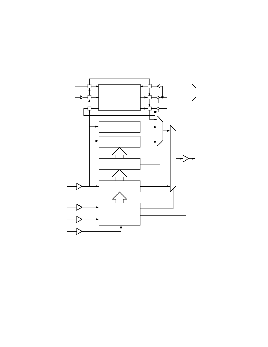
P60ARM-B
94
8.6 Test Data Registers
Figure 33: Boundary Scan Block Diagram
illustrates the structure of the boundary scan logic.
Figure 33: Boundary Scan Block Diagram
8.6.1 Bypass Register
Purpose: This is a single bit register which can be selected as the path between
TDI
and
TDO
to allow the
device to be bypassed during boundary-scan testing.
Length: 1 bit
Operating Mode: When the BYPASS instruction is the current instruction in the instruction register, serial
data is transferred from
TDI
to
TDO
in the SHIFT-DR state with a delay of one
TCK
cycle.
ARM
Core Logic
Instruction Register
Instruction Decoder
Device ID Register
Bypass Register
TAP
Controller
nTDOEN
nTRST
TCK
TMS
TDI
TDO
BSOUTCELL
BSOUTCELL
BSINCELL
I/O
Cell
BSOUTNENCELL
BSINCELL
BSINENCELL

Boundary Scan Test Interface
95
There is no parallel output from the bypass register.
A logic 0 is loaded from the parallel input of the bypass register in the CAPTURE-DR state.
8.6.2 ARM60 Device Identi�cation (ID) Code Register
Purpose: This register is used to read the 32-bit device identification code. No programmable
supplementary identification code is provided.
Length: 32 bits
The format of the ID register is as follows:
Please contact your supplier for the correct Device Identification Code.
Operating Mode: When the IDCODE instruction is current, the ID register is selected as the serial path
between
TDI
and
TDO
.
There is no parallel output from the ID register.
The 32-bit device identification code is loaded into the ID register from its parallel inputs during the
CAPTURE-DR state.
8.6.3 ARM60 Boundary Scan (BS) Register
Purpose: The BS register consists of a serially connected set of cells around the periphery of the device, at
the interface between the core logic and the system input/output pads. This register can be used to isolate
the core logic from the pins and then apply tests to the core logic, or conversely to isolate the pins from the
core logic and then drive or monitor the system pins.
Operating modes: The BS register is selected as the register to be connected between
TDI
and
TDO
only
during the SAMPLE/PRELOAD, EXTEST and INTEST instructions. Values in the BS register are used, but
are not changed, during the CLAMP and CLAMPZ instructions.
In the normal (system) mode of operation, straight-through connections between the core logic and pins are
maintained and normal system operation is unaffected.
In TEST mode (i.e. when either EXTEST or INTEST is the currently selected instruction), values can be
applied to the core logic or output pins independently of the actual values on the input pins and core logic
outputs respectively. On the ARM60 all of the boundary scan cells include an update register and thus all
of the pins can be controlled in the above manner. Additional boundary-scan cells are interposed in the scan
chain in order to control the enabling of tristateable buses.
0
1
11
12
27
28
31
1
Manufacturer Identity
Part Number
Version

P60ARM-B
96
The correspondence between boundary-scan cells and system pins, system direction controls and system
output enables is as shown in
Table 25: Boundary Scan Signals & Pins
. The cells are listed in the order in
which they are connected in the boundary-scan register, starting with the cell closest to
TDI
. All boundary-
scan register cells at input pins can apply tests to the on-chip core logic.
The EXTEST guard values specified in
Table 25: Boundary Scan Signals & Pins
should be clocked into the
boundary-scan register (using the SAMPLE/PRELOAD instruction) before the EXTEST instruction is
selected, to ensure that known data is applied to the core logic during the test. The INTEST guard values
shown in the table below should be clocked into the boundary-scan register (using the SAMPLE/
PRELOAD instruction) before the INTEST instruction is selected to ensure that all outputs are disabled.
These guard values should also be used when new EXTEST or INTEST vectors are clocked into the
boundary-scan register.
The values stored in the BS register after power-up are not defined. Similarly, the values previously clocked
into the BS register are not guaranteed to be maintained across a Boundary Scan reset (from forcing nTRST
LOW or entering the Test Logic Reset state).
8.6.4 Output Enable Boundary-scan Cells
The boundary-scan register cells Nendout, Nabe, Ntbe, and Nmse control the output drivers of tristate
outputs as shown in the table 25. In the case of OUTEN0 enable cells (Nendout, Ntbe), loading a 1 into the
cell will place the associated drivers into the tristate state, while in the case of type INEN1 enable cells
(Nabe, Nmse), loading a 0 into the cell will tristate the associated drivers.
To put all ARM60 tristate outputs into their high impedance state, a logic 1 should be clocked into the
output enable boundary-scan cells Nendout and Ntbe, and a logic 0 should be clocked into Nabe and Nmse.
Alternatively, the HIGHZ instruction can be used.
If the on-chip core logic causes the drivers controlled by Nendout, for example, to be tristate, (i.e. by driving
the signal Nendout HIGH), then a 1 will be observed on this cell if the SAMPLE/PRELOAD or INTEST
instructions are active.
8.6.5 Single-step Operation
ARM60 is a static design and there is no minimum clock speed. It can therefore be single-stepped while the
INTEST instruction is selected. This can be achieved by serialising a parallel stimulus and clocking the
resulting serial vectors into the boundary-scan register. When the boundary-scan register is updated, new
test stimuli are applied to the core logic inputs; the effect of these stimuli can then be observed on the core
logic outputs by capturing them in the boundary-scan register.

Boundary Scan Test Interface
97
8.7 Boundary Scan Interface Signals
Figure 34: Boundary Scan General Timing
Figure 35: Boundary Scan Tri-state Timing
Figure 36: Boundary Scan Reset Timing
TCK
TMS
TDI
TDO
Data In
Data Out
T
bscl
T
bsch
T
bsis
T
bsih
T
bsoh
T
bsod
T
bsss
T
bssh
T
bsdh
T
bsdd
TCK
TDO
Data Out
T
bsoe
T
bsoz
T
bsde
T
bsdz
nTRST
TMS
T
bsr
T
bsrs
T
bsrh

P60ARM-B
98
Notes:
1.
TCK
may be stopped indefinitely in either the low or high phase.
2.
Assumes a 25pF load on TDO. Output timing derates at 0.072ns/pF of extra load applied.
3.
TDO
enable time applies when the TAP controller enters the Shift-DR or Shift-IR states.
4.
TDO
disable time applies when the TAP controller leaves the Shift-DR or Shift-IR states.
5.
For correct data latching, the I/O signals (from the core and the pads) must be setup and held with
respect to the rising edge of TCK in the CAPTURE-DR state of the SAMPLE/PRELOAD, INTEST
and EXTEST instructions.
6.
Assumes that the data outputs are loaded with the AC test loads (see AC parameter specification).
7.
Data output enable time applies when the boundary scan logic is used to enable the output drivers.
8.
Data output disable time applies when the boundary scan is used to disable the output drivers.
9.
TMS
must be held high as nTRST is taken high at the end of the boundary-scan reset sequence.
Symbol
Parameter
Min
Typ
Max
Units
Notes
Tbscl
TCK low period
48
ns
1
Tbsch
TCK high p
eriod
48 ns
1
Tbsis
TDI,TMS setup to [TCr]
10
ns
Tbsih
TDI,TMS hold from [TCr]
10
ns
Tbsod TCf
to
TDO valid
40
ns
2
Tbsoh
TDO hold time
3
ns
2
Tbsoe
TDO enable time
5
ns
2,3
Tbsoz
TDO disable time
40
ns
2,4
Tbsss
I/O signal setup to [TCr]
10
ns
5
Tbssh
I/O signal hold from [TCr]
15
ns
5
Tbsdd
TCf to data output valid
30
ns
Tbsdh
data output hold time
3
ns
6
Tbsde
data output enable time
5
ns
6,7
Tbsdz
data output disable time
20
ns
6,8
Tbsr Reset
period
20
ns
Tbsrs
tms setup to [TRr]
10
ns
9
Tbsrh
tms hold from [TRr]
10
ns
9
Table 24: ARM60 Boundary Scan Interface Timing
99
No.
Output enable
Cell Name Pin Type BS Cell
Guard
Value
IN EX *
No.
Output enable
Cell Name Pin Type BS Cell
Guard
Value
IN EX *
from tdi
49
din24
D[24]
IN
-
*
0
1
din0
D[0]
IN
-
*
0
50
dout24
D[24]
OUT
Nenout=0
0
*
2
dout0
D[0]
OUT
Nenout=0
0
*
51
din25
D[25]
IN
-
*
0
3
din1
D[1]
IN
-
*
0
52
dout25
D[25]
OUT
Nenout=0
0
*
4
dout1
D[1]
OUT
Nenout=0
0
*
53
din26
D[26]
IN
-
*
0
5
din2
D[2]
IN
-
*
0
54
dout26
D[26]
OUT
Nenout=0
0
*
6
dout2
D[2]
OUT
Nenout=0
0
*
55
din27
D[27]
IN
-
*
0
7
din3
D[3]
IN
-
*
0
56
dout27
D[27]
OUT
Nenout=0
0
*
8
dout3
D[3]
OUT
Nenout=0
0
*
57
din28
D[28]
IN
-
*
0
9
din4
D[4]
IN
-
*
0
58
dout28
D[28]
OUT
Nenout=0
0
*
10
dout4
D[4]
OUT
Nenout=0
0
*
59
din29
D[29]
IN
-
*
0
11
din5
D[5]
IN
-
*
0
60
dout29
D[29]
OUT
Nenout=0
0
*
12
dout5
D[5]
OUT
Nenout=0
0
*
61
din30
D[30]
IN
-
*
0
13
din6
D[6]
IN
-
*
0
62
dout30
D[30]
OUT
Nenout=0
0
*
14
dout6
D[6]
OUT
Nenout=0
0
*
63
din31
D[31]
IN
-
*
0
15
din7
D[7]
IN
-
*
0
64
dout31
D[31]
OUT
Nenout=0
0
*
16
dout7
D[7]
OUT
Nenout=0
0
*
65
cpa
CPA
IN
-
*
1
17
din8
D[8]
IN
-
*
0
66
Nenout
-
OUTEN0
-
1
*
18
dout8
D[8]
OUT
Nenout=0
0
*
67
Nce
OUTEN0
-
1
*
19
din9
D[9]
IN
-
*
0
68
lock
LOCK
OUT
Nce=0
0
*
20
dout9
D[9]
OUT
Nenout=0
0
*
69
bigend
BIGEND
IN
-
*
0
21
din10
D[10]
IN
-
*
0
70
Ncpi
nCPI
OUT
Nce=0
0
*
22
dout10
D[10]
OUT
Nenout=0
0
*
71
dbe
DBE
IN
-
*
0
23
din11
D[11]
IN
-
*
0
72
Nbw
nBW
OUT
Nce=0
0
*
24
dout11
D[11]
OUT
Nenout=0
0
*
73
mclk
MCLK
IN
-
*
0
25
din12
D[12]
IN
-
*
0
74
Nwait
nWAIT
IN
-
*
0
26
dout12
D[12]
OUT
Nenout=0
0
*
75
lateabt
LATEABT
IN
-
*
1
27
din13
D[13]
IN
-
*
0
76
prog32
PROG32
IN
-
*
1
28
dout13
D[13]
OUT
Nenout=0
0
*
77
data32
DATA32
IN
-
*
1
29
din14
D[14]
IN
-
*
0
78
Nrw
nRW
OUT
Nce=0
0
*
30
dout14
D[14]
OUT
Nenout=0
0
*
79
Nopc
nOPC
OUT
Nce=0
0
*
31
din15
D[15]
IN
-
*
0
80
Nmreq
nMREQ
OUT
Nce=0
0
*
32
dout15
D[15]
OUT
Nenout=0
0
*
81
seq
SEQ
OUT
Nce=0
0
*
33
din16
D[16]
IN
-
*
0
82
abort
ABORT
IN
-
*
0
34
dout16
D[16]
OUT
Nenout=0
0
*
83
Nirq
nIRQ
IN
-
*
1
35
din17
D[17]
IN
-
*
0
84
Nfiq
nFIQ
IN
-
*
1
36
dout17
D[17]
OUT
Nenout=0
0
*
85
Nreset
nRESET
IN
-
*
0
37
din18
D[18]
IN
-
*
0
86
ale
ALE
IN
-
*
1
38
dout18
D[18]
OUT
Nenout=0
0
*
87
cpb
CPB
IN
-
*
1
39
din19
D[19]
IN
-
*
0
88
Ntrans
nTRANS
OUT
Nce=0
0
*
40
dout19
D[19]
OUT
Nenout=0
0
*
89
a31
A[31]
OUT
ABE=1
0
*
41
din20
D[20]
IN
-
*
0
90
a30
A[30]
OUT
ABE=1
0
*
42
dout20
D[20]
OUT
Nenout=0
0
*
91
a29
A[29]
OUT
ABE=1
0
*
43
din21
D[21]
IN
-
*
0
92
a28
A[28]
OUT
ABE=1
0
*
44
dout21
D[21]
OUT
Nenout=0
0
*
93
a27
A[27]
OUT
ABE=1
0
*
45
din22
D[22]
IN
-
*
0
94
a26
A[26]
OUT
ABE=1
0
*
46
dout22
D[22]
OUT
Nenout=0
0
*
95
a25
A[25]
OUT
ABE=1
0
*
47
din23
D[23]
IN
-
*
0
96
a24
A[24]
OUT
ABE=1
0
*
48
dout23
D[23]
OUT
Nenout=0
0
*
97
a23
A[23]
OUT
ABE=1
0
*
100
P60ARM-B
Table 25: Boundary Scan Signals & Pins
Key:
IN
Input pad
OUT
Output pad
NEN1
Input enable active high
OUTENO
Output enable active low
*
Guard Value for INTEST and EXTEST/CLAMP
98
a22
A[22]
OUT
ABE=1
0
*
111
a09
A[9]
OUT
ABE=1
0
*
99
a21
A[21]
OUT
ABE=1
0
*
112
a08
A[8]
OUT
ABE=1
0
*
100
a20
A[20]
OUT
ABE=1
0
*
113
a07
A[7]
OUT
ABE=1
0
*
101
a19
A[19]
OUT
ABE=1
0
*
114
a06
A[6]
OUT
ABE=1
0
*
102
a18
A[18]
OUT
ABE=1
0
*
115
a05
A[5]
OUT
ABE=1
0
*
103
a17
A[17]
OUT
ABE=1
0
*
116
a04
A[4]
OUT
ABE=1
0
*
104
a16
A[16]
OUT
ABE=1
0
*
117
a03
A[3]
OUT
ABE=1
0
*
105
a15
A[15]
OUT
ABE=1
0
*
118
a02
A[2]
OUT
ABE=1
0
*
106
a14
A[14]
OUT
ABE=1
0
*
119
a01
A[1]
OUT
ABE=1
0
*
107
a13
A[13]
OUT
ABE=1
0
*
120
a00
A[0]
OUT
ABE=1
0
*
108
a12
A[12]
OUT
ABE=1
0
*
121
abe
ABE
INEN1
-
0
*
109
a11
A[11]
OUT
ABE=1
0
*
to tdo
110
a10
A[10]
OUT
ABE=1
0
*
No.
Output enable
Cell Name Pin Type BS Cell
Guard
Value
IN EX *
No.
Output enable
Cell Name Pin Type BS Cell
Guard
Value
IN EX *

DC Parameters
101
9.0 DC Parameters
9.1 Absolute Maximum Ratings
NOTES:
These are stress ratings only. Exceeding the absolute maximum ratings may permanently damage the
device. Operating the device at absolute maximum ratings for extended periods may affect device
reliability. Functional operation of the device at these or any other condition outside those specified is not
implied.
The device contains circuitry designed to provide protection from damage by static discharge. It is
nonetheless recommended that precautions be taken to avoid applying voltages outside the specified
range.
All voltages are measured with respect to VSS.
(1) Not more than one output should be shorted to VDD or VSS at any one time.
Symbol
Parameter
Min
Typ
Max
Units
Notes
VDD
Supply voltage
0.0
7.0
V
Vip
Voltage applied to input pin
-0.5
7.0
V
Vop
Voltage applied to output pin
-0.5
Vdd+0.3
V
Osct
Output short circuit time
1
S
1
Ts
Storage temperature
-65
150
deg.C
Ta
Ambient operating temperature
-10
85
deg.C
Pd
Maximum power dissipation
2.0
W
Table 26: ARM60 DC Parameters - maximum ratings

102
P60ARM-B
9.2 DC Operating Conditions
Notes:
Voltages measured with respect to VSS.
(1)
Theses levels apply to all inputs of type I and IP. Particular care needs to be taken with clock inputs
in the PCB layout to eliminate EMC noise and provide true supply voltages directly at the device
pins.
9.3 DC Characteristics
Given VDD = 5.0V
�
10%, Ta = 0 to 70
�
C
Notes:
Voltages measured with respect to VSS.
(1)
All IP inputs at VDD.
(2)
This value represents the current that the input/output pins can tolerate before the chip latches up.
As sustained latch-up is catastrophic, this current must never be approached.
Symbol
Parameter
Min
Typ
Max
Units
Notes
VDD
Supply voltage
4.5
5.0
5.5
V
Vih
Input HIGH voltage
2.4
VDD
V
1
Vil
Input LOW voltage
0.0
0.8
V
1
Io4
Output current (O4 outputs)
+/-4
mA
Io8
Output current (OS8 outputs)
+/-8
mA
Ta
Ambient operating temperature
-40
+85
deg.C
Table 27: ARM60-B DC Operating Conditions
Symbol
Parameter
Min
Typ
Max
Units
Notes
Idd
static Supply current
50
�
A
1
Ilatch
DC latch-up current
100
mA
2
Iin
Input leakage current
+/-10
�
A
3
Vol
Output LOW voltage
0.4
V
4
Voh
Output HIGH voltage
2.4
V
4
Rp
�IP� input pullup resistor
35k
100k
ohm
5
Cin
Input capacitance
5
pF
ESD
HBM model ESD
2
kV
Table 28: ARM60 DC Characteristics

DC Parameters
103
(3)
For Vin = 0 to VDD and only for inputs without pullup resistors.
(4)
When sourcing or sinking the maximum rated output current for the output driver ( 4 or 8mA).
(5)
Only certain inputs have pullup resistors.

104
P60ARM-B

AC Parameters
105
10.0 AC Parameters
The AC timing diagrams presented in this section assume that the outputs of the ARM60 have been loaded
with the capacitive loads shown in the `Test Load' column of
Table 29: AC Test Loads
. These loads have been
chosen as typical of the type of system in which ARM60 might be employed.
The output drivers of the ARM60 are CMOS inverters which exhibit a propagation delay that increases
linearly with the increase in load capacitance. An `Output derating' figure is given for each output driver,
showing the approximate rate of increase of output time with increasing load capacitance.
Output
Signal
Test
Load
(pF)
Output
derating
(ns/pF)
D[31:0]
50
0.072
A[31:0]
50
0.072
LOCK
25
0.072
nCPI
25
0.093
nMREQ
25
0.093
SEQ
25
0.093
nRW
25
0.072
nBW
25
0.072
nOPC
25
0.093
nTRANS
25
0.072
TDO
25
0.072
Table 29: AC Test Loads
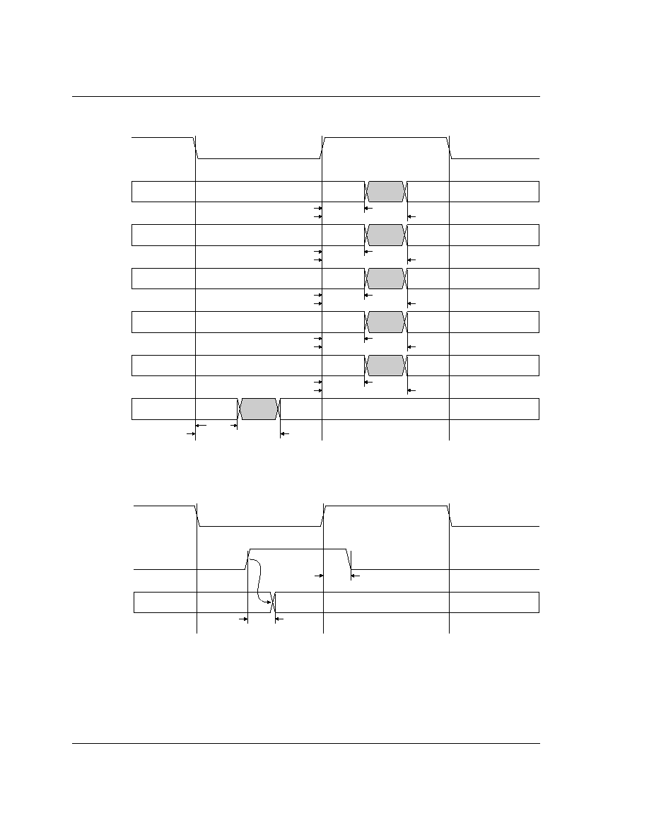
106
P60ARM-B
Figure 37: General Timings
Note:
nWAIT
,
ABE
and
ALE
are all HIGH during the cycle shown.
Figure 38: Address Timing
Note:
Tald is the time by which
ALE
must be driven LOW in order to latch the current address in phase
2. If
ALE
is driven low after Tald, then a new address may be latched.
ABE
is high during the cycle
shown.
MCLK
A[31:0]
nRW
nBW,
LOCK
nTRANS
nOPC
nMREQ,
SEQ
T
ah
T
addr
T
rwh
T
rwd
T
blh
T
bld
T
mdh
T
mdd
T
opch
T
opcd
T
msh
T
msd
MCLK
ALE
A[31:0]
T
ald
T
ale

AC Parameters
107
Figure 39: Address Control
Note:
Tabz is the tristate turn off time, Tabe is the address enable time (turn on), relative to
ABE
.
ALE
is
high during the cycle shown.
Figure 40: Data Write Cycle
Note:
DBE
is high during the cycle shown.
Figure 41: Data Read Cycle
Note:
DBE
is high during the cycle shown.
MCLK
ABE
A[31:0]
T
abz
T
abe
T
addr
MCLK
D[31:0]
T
dout
T
doh
MCLK
D[31:0]
T
dis
T
dih
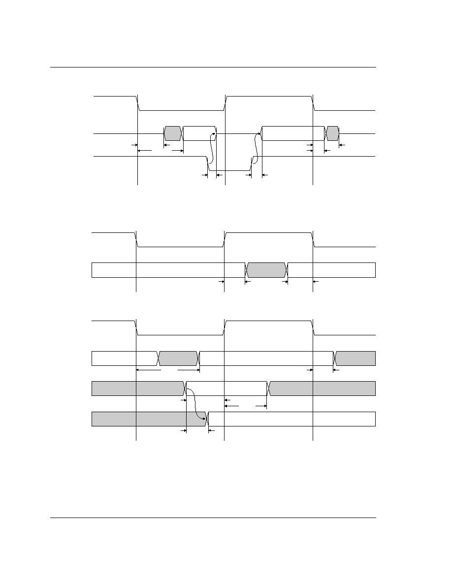
108
P60ARM-B
Figure 42: Data Bus Control
Note:
The cycle shown is a data write cycle. Here,
DBE
has been used to modify the behaviour of the data
bus.
Figure 43: Configuration Pin Timing
Figure 44: Coprocessor Timing
Note:
Normally,
nMREQ
and
SEQ
become valid Tmsd after the falling edge of
MCLK
. In this cycle the
ARM has been busy-waiting, waiting for a coprocessor to complete the instruction. If
CPA
and
CPB
change during phase 1, the timing of
nMREQ
and
SEQ
will depend on Tcpms. Most systems
should be able to generate
CPA
and
CPB
during the previous phase 2, and so the timing of
nMREQ
and
SEQ
will always be Tmsd.
MCLK
D[31:0]
DBE
T
de
T
dout
T
doh
T
dz
T
dbz
T
dbe
MCLK
LATEABT,
BIGEND,
DATA32,
PROG32
T
cth
T
cts
MCLK
nCPI
CPA, CPB
nMREQ,
SEQ
T
cpi
T
cpih
T
cps
T
cph
T
cpms
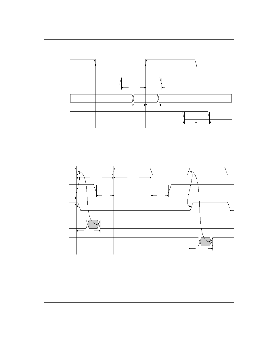
AC Parameters
109
Figure 45: Exception Timing
Note:
Tirs, Trs guarantee recognition of the interrupt (or reset) source by the corresponding clock edge.
Tirm, Trh guarantee non-recognition by that clock edge. These inputs may be applied fully
asynchronously where the exact cycle of recognition is unimportant.
Figure 46: Clock Timing
Note:
The ARM core is not clocked by the HIGH phase of
MCLK
enveloped by
nWAIT
. Thus, during the
cycles shown,
nMREQ
and
SEQ
change once, during the first LOW phase of
MCLK
, and
A[31:0]
change once, during the second HIGH phase of
MCLK
. For reference, ph2 is shown. This is the
internal clock from which the core times all its activity. This signal is included to show how the high
phase of the external
MCLK
has been removed from the internal core clock.
MCLK
ABORT
nRESET
nFIQ, nIRQ
T
abts
T
abth
T
rs
T
rh
T
irs
T
irm
MCLK
nWAIT
ph2
nMREQ/
SEQ
A[31:0]
T
clkl
T
clkh
T
ws
T
wh
T
msd
T
addr

110
P60ARM-B
Symbol
Parameter
P60ARM*
P60ARM-B
Min
Max
Min
Max
Tckl
clock LOW time
23
16
Tckh
clock HIGH time
23
16
Tws
nWAIT setup to CKr
3
3
Twh
nWAIT hold from CKf
3
3
Tale
address latch open
0
15
0
14
Tald
address latch time
1
1
Taddr
CKr to address valid
22
20
Tah
address hold time
6
5
Tdbz
Data bus tristate time from DBE
3
12
3
12
Tdbe
Data bus enable time from DBE
3
13
3
13
Tabz
Address bus disable from ABE
3
12
3
12
Tabe
Address bus enable from ABE
3
13
3
13
Tde
Data bus enable from MCLK
10
9
Tdz
Data bus disable from MCLK
10
10
Tdout
data out delay
28
22
Tdoh
data out hold
3
3
Tdis
data in setup
3
2
Tdih
data in hold
6
6
Tabts
ABORT setup time
5
5
Tabth
ABORT hold time
3
3
Trs
RESET Setup time
6
6
Trh
RESET hold time
6
6
Tirs interrupt
setup
6
4
Tirm
Interrupt non-recognition time
6
4
Trwd
CKr to nRW valid
23
21
Trwh
nRW hold time
3
3
Tmsd
CKf to nMREQ & SEQ
26
22
Tmsh
nMREQ & SEQ hold time
3
3
Tbld
CKr to nBW & LOCK
23
21
Tblh
nBW & LOCK hold
3
3
Tmdd
CKr to nTRANS
23
21
Tmdh
nTRANS hold time
3
3
Topcd
CKr to nOPC valid
16
16
Topch
nOPC hold time
3
3
Tcps
CPA, CPB setup
7*
12
Tcph
CPA,CPB hold time
3
3
Tcpms
CPA, CPB to nMREQ, SEQ
16
16
Tcpi
CKf to nCPI delay
16
16
Tcpih
nCPI hold time
3
3
Tcts
Config setup time
2
2
Tcth
Config hold time
2
2
Table 30: AC Parameters (units of nS)

AC Parameters
111
* Note:
Table 30 also includes data fpr the obsolete P60ARM for convenience. Customers replacing the
P60ARM by the P60ARM-B should check that timing differences betweem the two devices will
not cause operational problems. Note in particular that Tah and Tde are marginally less for the
-B version. In the case of Tcps, the figure of 7 ns for the P60ARM was incorrect. The correct
figure for both processors is 12 ns.
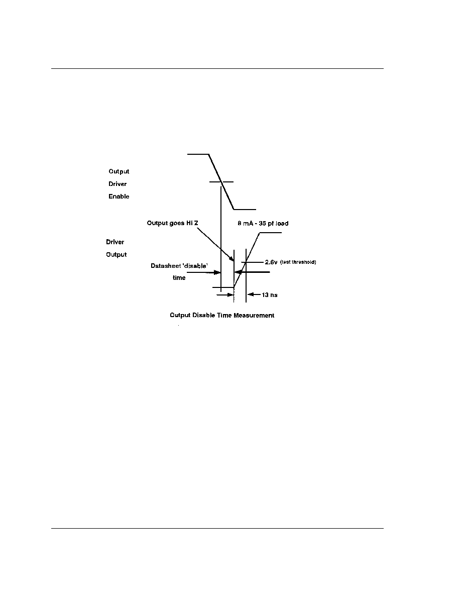
112
P60ARM-B
10.1 Notes on AC Parameters
1.
Tristate output times:
2.
For a valid RESET, NRESET must remain low for a minimum of two MCLK cycles.

Physical Details
113
11.0 Physical Details
Figure 47: ARM60 100 Pin Metric Plastic QFP Mechanical Dimensions in mm
17.90
�
0.25
14.00
�
0.10
0.65 typ
0.30
2.80
�
0.25
ARM60
Pin 30
Pin 1
Pin 31
Pin 50
Pin 51
Pin 80
Pin 81
Pin 100
23.90
�
0.25
20.00
�
0.10
0.83
�
0.15
3.40 max

114
P60ARM-B
Pinout
115
12.0 Pinout
Pin
Signal
Type
Pin
Signal
Type
Pin
Signal
Type
1
D[27]
i/o
41
A[20]
o
81
Vdd
-
2
D[28]
i/o
42
A[19]
o
82
D[8]
i/o
3
D[29]
i/o
43
A[18]
o
83
D[9]
i/o
4
D[30]
i/o
44
A[17]
o
84
D[10]
i/o
5
D[31]
i/o
45
A[16]
o
85
D[11]
i/o
6
CPA
i
46
A[15]
o
86
D[12]
i/o
7
Vss
-
47
A[14]
o
87
D[13]
i/o
8
Vdd
-
48
A[13]
o
88
D[14]
i/o
9
LOCK
o
49
A[12]
o
89
D[15]
i/o
10
BIGEND
i
50
A[11]
o
90
D[16]
i/o
11
nCPI
o
51
Vdd
-
91
D[17]
i/o
12
DBE
i
52
Vss
-
92
D[18]
i/o
13
nBW
o
53
A[10]
o
93
D[19]
i/o
14
MCLK
i
54
A[9]
o
94
D[20]
i/o
15
nWAIT
i
55
A[8]
o
95
D[21]
i/o
16
LATEABT
i
56
A[7]
o
96
D[22]
i/o
17
PROG32
i
57
A[6]
o
97
D[23]
i/o
18
DATA32
i
58
A[5]
o
98
D[24]
i/o
19
nRW
o
59
A[4]
o
99
D[25]
i/o
20
nOPC
o
60
A[3]
o
100
D[26]
i/o
21
nMREQ
o
61
A[2]
o
22
SEQ
o
62
A[1]
o
23
ABORT
i
63
A[0]
o
24
nIRQ
i
64
Vss
-
25
nFIQ
i
65
Vdd
-
26
nRESET
i
66
ABE
i
27
ALE
i
67
TCK
i
28
CPB
i
68
TMS
i
29
nTRANS
o
69
nTRST
i
30
A[31]
o
70
TDI
i
31
A[30]
o
71
TDO
o
32
A[29]
o
72
D[0]
i/o
33
A[28]
o
73
D[1]
i/o
34
A[27]
o
74
D[2]
i/o
35
A[26]
o
75
D[3]
i/o
36
A[25]
o
76
D[4]
i/o
37
A[24]
o
77
D[5]
i/o
38
A[23]
o
78
D[6]
i/o
39
A[22]
o
79
D[7]
i/o
40
A[21]
o
80
Vss
-
Table 31: Pinout - ARM60 100 pin Plastic Quad Flat Pack

www.zarlink.com
Information relating to products and services furnished herein by Zarlink Semiconductor Inc. trading as Zarlink Semiconductor or its subsidiaries (collectively
"Zarlink") is believed to be reliable. However, Zarlink assumes no liability for errors that may appear in this publication, or for liability otherwise arising from the
application or use of any such information, product or service or for any infringement of patents or other intellectual property rights owned by third parties which may
result from such application or use. Neither the supply of such information or purchase of product or service conveys any license, either express or implied, under
patents or other intellectual property rights owned by Zarlink or licensed from third parties by Zarlink, whatsoever. Purchasers of products are also hereby notified
that the use of product in certain ways or in combination with Zarlink, or non-Zarlink furnished goods or services may infringe patents or other intellectual property
rights owned by Zarlink.
This publication is issued to provide information only and (unless agreed by Zarlink in writing) may not be used, applied or reproduced for any purpose nor form part
of any order or contract nor to be regarded as a representation relating to the products or services concerned. The products, their specifications, services and other
information appearing in this publication are subject to change by Zarlink without notice. No warranty or guarantee express or implied is made regarding the
capability, performance or suitability of any product or service. Information concerning possible methods of use is provided as a guide only and does not constitute
any guarantee that such methods of use will be satisfactory in a specific piece of equipment. It is the user's responsibility to fully determine the performance and
suitability of any equipment using such information and to ensure that any publication or data used is up to date and has not been superseded. Manufacturing does
not necessarily include testing of all functions or parameters. These products are not suitable for use in any medical products whose failure to perform may result in
significant injury or death to the user. All products and materials are sold and services provided subject to Zarlink's conditions of sale which are available on request.
Purchase of Zarlink's I
2
C components conveys a licence under the Philips I
2
C Patent rights to use these components in an I
2
C System, provided that the system
conforms to the I
2
C Standard Specification as defined by Philips.
Zarlink, ZL and the Zarlink Semiconductor logo are trademarks of Zarlink Semiconductor Inc.
Copyright 2003, Zarlink Semiconductor Inc. All Rights Reserved.
TECHNICAL DOCUMENTATION - NOT FOR RESALE
For more information about all Zarlink products
visit our Web Site at