DS2219 - 2.4
SP4666
Prescaler with low current and low radiation
The SP4666 is a selectable division ratio high speed divider
capable of replacing separate fixed ratio ECL prescalers with a
single part in applications with alternative 464 and 4256 division
requirements.
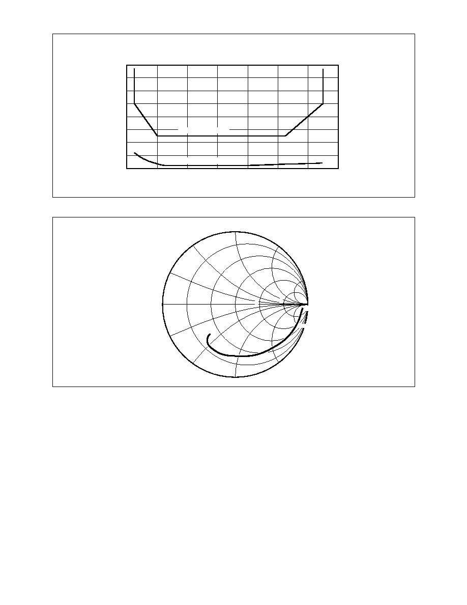
A switched low pass filter with 23dB points at 5�3MHz and
15�6MHz is connected before the output stage to reduce the
harmonic content to a very low level.
FEATURES
s
Switched Low Pass Filter for Very Low Output Radiation
s
Low Supply Current
s
Input Wideband Amplifier
s
High Input Sensitivity
s
High Input Impedance
s
Balanced ECL Outputs
s
Electrostatic Protection
ESD precautions must be observed
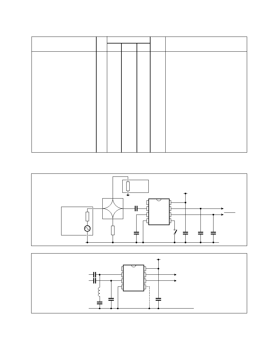
Fig. 2 SP4666 block diagram
1k
V
CC
1k
INPUTS
2
3
5
OUTPUTS
0V
7
6
8
4
500
500
2k
2k
4
64/4256
V
CC
20k
10k
50
�
A
2mA
4
64/4256 SELECT
FILTER
1
7V
2�5V p-p
2
55
�
C to 1150
�
C
0
�
C to180
�
C
ABSOLUTE MAXIMUM RATINGS
Supply voltage, V
CC
Input voltage
Storage temperature
Operating temperature range
ORDERING INFORMATION
SP4666 NA DP
SP4666 NA MP
Fig 1. Pin connections - top view
MP8
DP8
NC
INPUT
INPUT
0V
1
5V
OUTPUT
OUTPUT
4
64 /4256 SELECT
1
2
3
4
8
7
6
5
1
2
3
4
8
7
6
5
1
1
5V
OUTPUT
OUTPUT
4
64 /4256 SELECT
NC
INPUT
INPUT
0V
SP4666
SP4666
2
SP4666
ELECTRICAL CHARACTERISTICS
These characteristics are guaranteed over the following conditions (unless otherwise stated):
T
AMB
= 0
�
C to 180
�
C, V
CC
= 4�5V to 5�5V (Test circuit see Fig. 3)
Characteristic
Supply current, I
CC
Input sensitivity
50MHz
200MHz to 1050MHz
1050MHz to 1300MHz
Input overload
Input impedance
Output voltage with 12pF load
Output impedance
Output imbalance
Voltage for 4256 operation
Voltage for 464 operation
Sink current for 4256 operation
Conditions
Value
Typ.
Max.
Min.
Units
30
10
5
10
0�5
250
mA
mV
mV
mV
mV
pF
V p-p
V p-p
V p-p
V p-p
V p-p
V p-p
V
V
V
�
A
8
2,3
2,3
2,3
6,7
6,7
6,7
5
5
5
500
0�8
0�8
0�4
0�7
0�25
0�6
3�5
23
2�5
0�5
50
2
1
1
0�5
0�9
0�35
0�7
500
0�1
Pin
V
CC
= 15V
RMS sinewave (50
system)
See Fig. 6
4
64 mode, f
IN
= 100MHz
4
256 mode, f
IN
= 100MHz
4
64 mode, f
IN
= 1000MHz
4
256 mode, f
IN
= 1000MHz
4
64 mode, f
IN
= 1300MHz
4
256 mode, f
IN
= 1300MHz
See note 1
Vpin5 = 0V
Fig. 4 Application circuit
1
2
3
4
8
7
6
5
12p
1
5V
1n
0�1
�
OUTPUTS
0V
100p
1 TURN
1n
UHF INPUT
VHF INPUT
SP4666
NOTE: For 464 operation,
pin 5 may be left open
circuit or connected to 15V
Fig. 3 Test circuit
1n
1
5V
1n
180
�
HYBRID
COUPLER
0�1
�
OUTPUT
12p
12p
50
A
50
SIGNAL
GENERATOR
B
C
D
50
SAMPLING
SCOPE
0V
SP4666
1
2
3
4
8
7
6
5
OPEN = 464
CLOSED = 4256
OUTPUT
NOTES
1. Pin 5 has an internal pull-up and may be left open-circuit for 464 operation.
2. The difference between the maximum input sensitivity and minimum overload voltage is the guaranteed dynamic range. Input signal levels should
be maintained within these limits at all frequencies.

www.zarlink.com
Information relating to products and services furnished herein by Zarlink Semiconductor Inc. or its subsidiaries (collectively "Zarlink") is believed to be reliable.
However, Zarlink assumes no liability for errors that may appear in this publication, or for liability otherwise arising from the application or use of any such
information, product or service or for any infringement of patents or other intellectual property rights owned by third parties which may result from such application or
use. Neither the supply of such information or purchase of product or service conveys any license, either express or implied, under patents or other intellectual
property rights owned by Zarlink or licensed from third parties by Zarlink, whatsoever. Purchasers of products are also hereby notified that the use of product in
certain ways or in combination with Zarlink, or non-Zarlink furnished goods or services may infringe patents or other intellectual property rights owned by Zarlink.
This publication is issued to provide information only and (unless agreed by Zarlink in writing) may not be used, applied or reproduced for any purpose nor form part
of any order or contract nor to be regarded as a representation relating to the products or services concerned. The products, their specifications, services and other
information appearing in this publication are subject to change by Zarlink without notice. No warranty or guarantee express or implied is made regarding the
capability, performance or suitability of any product or service. Information concerning possible methods of use is provided as a guide only and does not constitute
any guarantee that such methods of use will be satisfactory in a specific piece of equipment. It is the user's responsibility to fully determine the performance and
suitability of any equipment using such information and to ensure that any publication or data used is up to date and has not been superseded. Manufacturing does
not necessarily include testing of all functions or parameters. These products are not suitable for use in any medical products whose failure to perform may result in
significant injury or death to the user. All products and materials are sold and services provided subject to Zarlink's conditions of sale which are available on request.
Purchase of Zarlink's I
2
C components conveys a licence under the Philips I
2
C Patent rights to use these components in and I
2
C System, provided that the system
conforms to the I
2
C Standard Specification as defined by Philips.
Zarlink, ZL and the Zarlink Semiconductor logo are trademarks of Zarlink Semiconductor Inc.
Copyright Zarlink Semiconductor Inc. All Rights Reserved.
TECHNICAL DOCUMENTATION - NOT FOR RESALE
For more information about all Zarlink products
visit our Web Site at