The SP5524 is a single-chip frequency synthesiser designed
for TV tuning systems. Control data is entered in the standard
I
2
C BUS format. The device has six controllable open-collector
output ports (P0-P3, P6 and P7), each capable of sinking
10mA. In addition, P1 is a 3-bit 5-level ADC input. The information
on these ports can be read via the I
2
C BUS.
The device has one fixed I
2
C BUS address and three
programmable addresses, allowing two or more synthesisers
to be used in a system.
FEATURES
s
Complete 1∑3GHz Single Chip System
s
Programmable via the I
2
C BUS
s
Low Power Consumption (215mW Typ.)
s
Low Radiation
s
Phase Lock Detector
s
Varactor Drive Amp Disable
s
6 Controllable Outputs, 4 Bi-directional
s
5-Level ADC
s
Variable I
2
C BUS Address for Picture in Picture TV
s
ESD Protection
*
*
Normal ESD handling precautions should be observed.
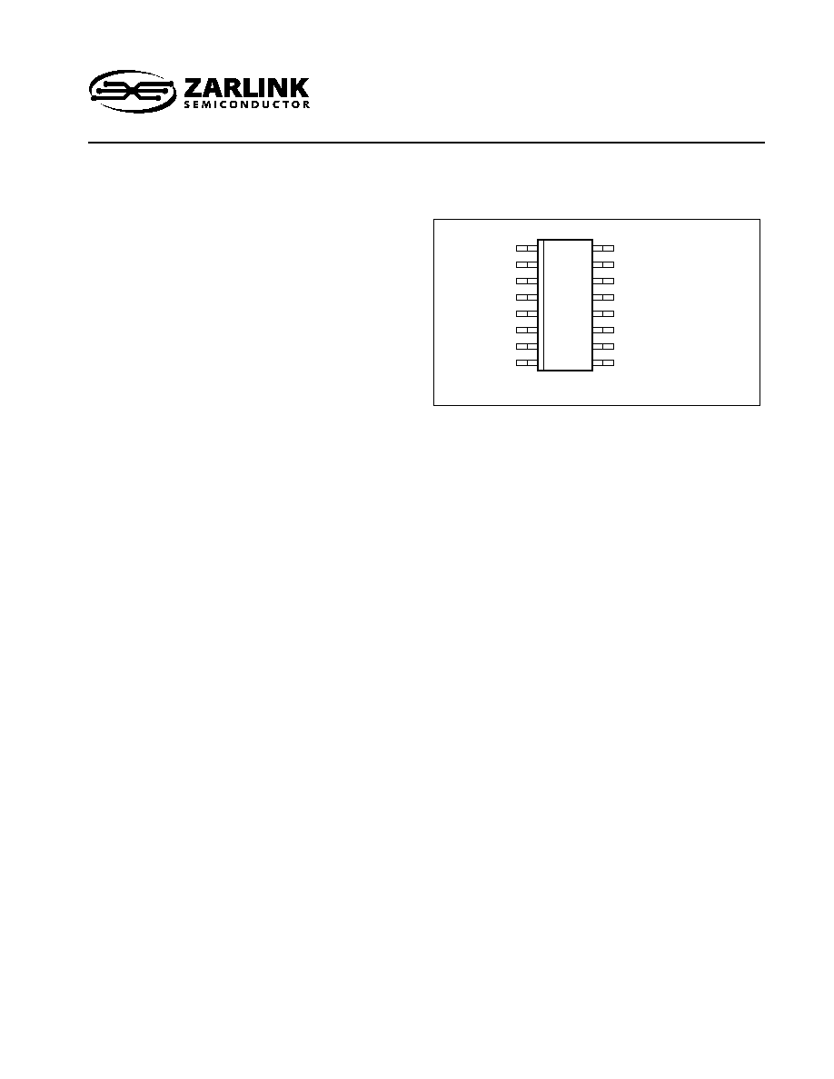
SP5524S
1
8
MP16
16
9
CHARGE PUMP
CRYSTAL Q1
CRYSTAL Q2
SDA
SCL
I/O PORT P0
*
I/O PORT P1
I/O PORT P2
DRIVE OUTPUT
V
EE
RF INPUT
RF INPUT
V
CC
P6 OUTPUT PORT
P7 OUTPUT PORT/ADD SELECT
I/O PORT P3
Fig. 1 Pin connections ≠ top view
APPLICATIONS
s
Satellite TV when Combined with SP4902
2∑5GHz Prescaler
s
Cable Tuning Systems
s
VCRs
ORDERING INFORMATION
SP5524S KG MPAS (Tubes)
SP5524S KG MPAD (Tape and Reel)
SP5524
Bidirectional I2C Bus Controlled Synthesiser
DS3900 - 2.1 March 1995

2
SP5524
ELECTRICAL CHARACTERISTICS
T
AMB
=
-
10
∞
C to +80
∞
C, V
CC
= +4∑5V to +5∑5V.
These Characteristics are guaranteed by either production test or design. They apply within the specified ambient temperature
and supply voltage ranges unless otherwise stated. Reference frequency 4MHz unless otherwise stated.
Supply current
Prescaler input voltage
Prescaler input impedance
Prescaler input capacitance
SDA, SCL
Input high voltage
Input low voltage
Input high current
Input low current
Leakage current
SDA
Output voltage
Charge pump current low
Charge pump current high
Charge pump output leakage current
Charge pump drive output current
Charge pump amplifier gain
Recommended crystal series resistance
Crystal oscillator drive level
Crystal oscillator negative resistance
Output Ports
P0-P3, P6, P7 sink current (see note 1)
P0-P3, P6, P7 leakage current (see note 1)
Input Ports
P7 input current high
P7 input current low
P0, P2, P3 input voltage low
P0, P2, P3 input voltage high
P1 input current high
P1 input current low
Typ.
Value
Conditions
Characteristic
Pin
12
13,14
13,14
4,5
4,5
4,5
4,5
4,5
4
1
1
1
16
2
6-11
6-11
10
10
6,8,9
6,8,9
7
7
12∑5
30
3
0
500
10
750
10
2∑7
43
50
2
±
50
±
170
6400
40
53
300
300
5∑5
1∑5
10
-10
10
0∑4
±
5
200
10
+10
-10
0∑8
+10
-10
Units
Min.
Max.
mA
mVrms
mVrms
pF
V
V
µ
A
µ
A
µ
A
V
µ
A
µ
A
nA
µ
A
mV p-p
mA
µ
A
µ
A
µ
A
V
V
µ
A
µ
A
V
CC
= 5V
100MHz to 1GHz
50MHz and 1∑3GHz, see Fig. 5
Input voltage = V
CC
Input voltage = 0V
When V
CC
= 0V
Sink current = 3mA
Byte 4, bit 2 = 0, pin 1 = 2V
Byte 4, bit 2 = 1, pin 1 = 2V
Byte 4, bit 4 = 1, pin 1 = 2V
V pin 16 = 0∑7V
Parallel resonant crystal (note 2)
V
OUT
= 0∑7V, see note 1
V
OUT
= 13∑2V
V pin 10 = 13∑2V
V pin 10 = 0V
See Table 3 for ADC levels
NOTES
1. Source impedance between all output ports and ground is approximately 5
. This should be taken into account when calculating output port
saturation voltages.
2. The recommended crystal series resistance quoted refers to all conditions including start-up.

4
SP5524
FUNCTIONAL DESCRIPTION
The SP5524 is programmed from an I
2
C BUS. Data and
Clock are fed in on the SDA and SCL lines respectively as
defined by the I
2
C Bus format. The synthesiser can either
accept new data (write mode) or send data (read mode). The
Tables in Fig. 3 illustrate the format of the data. The device
can be programmed to respond to several addresses, which
enables the use of more than one synthesiser in an I
2
C BUS
system. Table 4 shows how the address is selected by
applying a voltage to P7. The LSB of the address byte (R/W)
sets the device into read mode if it is high and write mode if
it is low. When the SP5524 receives a correct address byte
it pulls the SDA line low during the acknowledge period and
during following acknowledge periods after further data bytes
are programmed. When the SP5524 is programmed into the
read mode the controlling device accepting the data must pull
down the SDA line during the following acknowledge period
to read another status byte.
WRITE MODE (FREQUENCY SYNTHESIS)
When the device is in the write mode Bytes 2+3 select the
synthesised frequency while Bytes 4+5 select the output port
states and charge pump information.
Once the correct address is received and acknowledged,
the first bit of the next byte determines whether that byte is
interpreted as Byte 2 or 4, a logic 0 for frequency information
and a logic 1 for charge pump and output port information.
Additional data bytes can be entered without the need to re-
address the device until an I
2
C stop condition is recognised.
This allows a smooth frequency sweep for fine tuning or AFC
purposes.
If the transmission of data is stopped mid-byte (e.g., by
another device on the bus) then the previously programmed
byte is maintained.
Frequency data from Bytes 2 and 3 is stored in a 15-bit shift
register and is used to control the division ratio of the 15-bit
programmable divider which is preceded by a divide-by-8
prescaler and amplifier to give excellent sensitivity at the local
oscillator input; see Fig 5. The input impedance is shown in
Fig. 7.
The programmed frequency can be calculated by multiply-
ing the programmed division ratio by 8 times the comparison
frequency F
COMP
.
When frequency data is entered, the phase comparator,
via the charge pump and varactor drive amplifier, adjusts the
local oscillator control voltage until the output of the program-
mable divider is frequency and phase locked to the comparison
frequency.
The reference frequency may be generated by an external
source capacitively coupled into pin 2 or provided by an on-
chip 4MHz crystal controlled oscillator.
Note that the comparison frequency is 7∑8125kHz when a
4MHz reference is used.
Bit 2 of Byte 4 of the programming data (CP) controls the
current in the charge pump circuit, a logic 1 for
±
170
µ
A and
a logic 0 for
±
50
µ
A, allowing compensation for the variable
tuning slope of the tuner and also to enable fast channel
changes over the full band. Bit 4 of Byte 4 (T0) disables the
charge pump if set to a logic 1. Bit 8 of Byte 4 (OS) switches
the charge pump drive amplifier's output off when it is set to
a logic 1. Bit 3 of Byte 4 (T1) selects a test mode where the
phase comparator inputs are available on P6 and P7, a logic
1 connects F
COMP
to P6 and F
DIV
to P7.
Byte 5 programs the output ports P0-P3, P6 and P7, a logic
0 for a high impedance output, logic 1 for low impedance (on).
READ MODE
When the device is in the read mode the status data read
from the device on the SDA line takes the form shown in Table
2.
Bit 1 (POR) is the power on reset indicator and is set to a
logic 1 if the power supply to the device has dropped below a
nominal 3V and the programmed information lost (e.g., when
the device is initially turned on). The POR is set to 0 when the
read sequence is terminated by a stop command. The outputs
are all set to high impedance when the device is initially
powered up. Bit 2 (FL) indicates whether the device is phase
locked, a logic 1 is present if the device is locked and a logic
0 if the device is unlocked.
Bits 3, 4 and 5 (I2, I1, I0) show the status of the I/O Ports
P0, P2 and P3 respectively. A logic 0 indicates a low level and
a logic 1 a high level. If the ports are to be used as inputs they
should be programmed to a high impedance state (logic1).
These inputs will then respond to data complying with stand-
ard TTL voltage levels. Bits 6, 7 and 8 (A2,A1,A0) combine to
give the output of the 5-level ADC.
The 5-level ADC can be used to feed AFC information to
the microprocessor from the IF section of the television, as
illustrated in Fig. 4.

