SP5655
2∑7GHz Bidirectional I
2
C Bus Controlled Synthesiser
Datasheet
DS3743
ISSUE 5.2
November 2001
Ordering Information
SP5655CS/KG/MPAS (Tubes)
SP5655CS/KG/MPAD (Tape and reel)
The SP5655 is a single chip frequency synthesiser
designed for TV tuning systems. Control data is entered in
the standard I
2
C BUS format. The device contains 2
addressable current limited outputs and 4 addressable
bidirectional open-collector ports, one of which is a 3-bit
ADC. The information on these ports can be read via the I
2
C
BUS. the device has one fixed I
2
C BUS address and 3
programmable addresses, programmed by applying a specific
input voltage to one of the current limited outputs. This
enables two or more synthesisers to be used in a system.
FEATURES
s
Complete 2∑7GHz Single Chip System
s
High Sensitivity RF Inputs
s
Programmable via I
2
C BUS
s
Low Power Consumption (5V, 30mA)
s
Low Radiation
s
Phase Lock Detector
s
Varactor Drive Amp Disable
s
6 Controllable Outputs, 4 Bidirectional
s
5-Level ADC
s
Variable I
2
C BUS Address for Multi-tuner Applications
s
ESD Protection: 4kV, Mil-Std-883C, Method 3015
(1)
s
Switchable
4
512/1024 Reference Divider
s
Pin and Function Compatible with SP5055S
(2)
(1)
Normal ESD handling precautions should be observed.
(2) The SP5055S does not have a switchable reference
division ratio.
APPLICATIONS
s
Satellite TV
s
High IF Cable Tuning Systems
THERMAL DATA
u
JC
= 41
∞
C/W
u
JA
= 111
∞
C/W
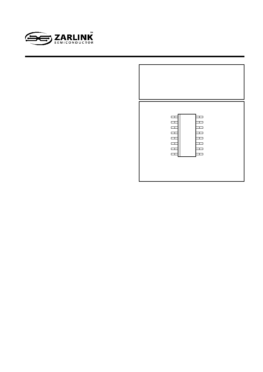
Fig. 1 Pin connections ≠ top view
SP5655
1
2
3
4
5
6
7
8
MP16
16
15
14
13
12
11
10
9
CHARGE PUMP
CRYSTAL Q1
CRYSTAL Q2
SDA
SCL
I/O PORT P7
*
I/O PORT P6
I/O PORT P5
DRIVE OUTPUT
V
EE
RF INPUT
RF INPUT
V
CC
P0 OUTPUT PORT
I/O PORT P4
= Logic level I/O port
*
= 3-bit ADC input
P3 OUTPUT PORT/
ADD SELECT

2
SP5655
Datasheet
ELECTRICAL CHARACTERISTICS
T
AMB
= -20
∞
C to +80
∞
C, V
CC
= +4∑5V to +5∑5V, reference frequency = 4MHz.
These Characteristics are guaranteed by either production test or design. They apply within the specified ambient temperature
and supply voltage ranges unless otherwise stated.
Supply current
Prescaler input voltage
Prescaler input impedance
Prescaler input capacitance
SDA, SCL
Input high voltage
Input low voltage
Input high current
Input low current
Leakage current
SDA
Output voltage
Charge pump current low
Charge pump current high
Charge pump output leakage current
Charge pump drive output current
Charge pump amplifier gain
Recommended crystal series resistance
Crystal oscillator drive level
Crystal oscillator negative resistance
External reference input frequency
External reference input amplitude
Output Ports
P0, P3 sink current
P0, P3 leakage current
P4-P7 sink current
P4-P7 leakage current
Input Ports
P3 input current high
P3 input current low
P4, P5, P7 input voltage low
P4, P5, P7 input voltage high
P6 input current high
P6 input current low
Typ.
Value
Conditions
Characteristic
Pin
12
13,14
13,14
13, 14
4,5
4,5
4,5
4,5
4,5
4
1
1
1
16
2
2
2
2
11, 10
11, 10
9-6
9-6
10
10
9,8,6
9,8,6
7
7
50
3
0
500
10
750
2
70
0∑7
10
2∑7
30
50
2
±
50
±
170
6400
80
1000
1
40
300
5∑5
1∑5
10
-10
10
0∑4
±
5
200
8
200
1∑5
10
10
+10
-10
0∑8
+10
-10
Units
Min.
Max.
mA
mVrms
pF
V
V
µ
A
µ
A
µ
A
V
µ
A
µ
A
nA
µ
A
mV p-p
MHz
mVrms
mA
µ
A
mA
µ
A
µ
A
µ
A
V
V
µ
A
µ
A
V
CC
= 4∑5V to 5∑5V (note 1)
120MHz to 2∑7GHz sinewave,
see Fig. 5
Input voltage = V
CC
Input voltage = 0V
When V
CC
= 0V
Sink current = 3mA
Byte 4, bit 2 = 0, pin 1 = 2V
Byte 4, bit 2 = 1, pin 1 = 2V
Byte 4, bit 4 = 1, pin 1 = 2V
V pin 16 = 0∑7V
Parallel resonant crystal (note 2)
AC coupled sinewave
AC coupled sinewave
V
OUT
= 12V
V
OUT
= 13∑2V
V
OUT
= 0∑7V
V
OUT
= 13∑2V
V pin 10 = V
CC
V pin 10 = 0V
See Table 3 for ADC levels
NOTES
1. Maximum power consumption is 220mW with V
CC
= 5∑5V and all ports off.
2. Resistance specified is maximum under all conditions.

4
SP5655
Datasheet
FUNCTIONAL DESCRIPTION
The SP5655 is programmed from an I
2
C Bus. Data and
Clock are fed in on the SDA and SCL lines respectively, as
defined by the I
2
C Bus format. The synthesiser can either
accept new data (write mode) or send data (read mode). The
LSB of the address byte (R/W) sets the device into write mode
if it is low and read mode if it is high. The Tables in Fig. 3
illustrate the format of the data. The device can be pro-
grammed to respond to several addresses, which enables the
use of more than one synthesiser in an I
2
C Bus system.
Table 4 shows how the address is selected by applying a
voltage to P3.
When the device receives a correct address byte, it pulls
the SDA line low during the acknowledge period, and during
following acknowledge periods after further data bytes are
programmed. When the device is programmed into the read
mode, the controller accepting the data must pull the SDA line
low during all status byte acknowledge periods to read an-
other status byte. If the controller fails to pull the SDA line low
during this period, the device generates an internal STOP
condition, which inhibits further reading.
WRITE Mode (Frequency Synthesis)
When the device is in write mode bytes 2 and 3 select the
synthesised frequency, while bytes 4 and 5 control the output
port states, charge pump, reference divider ratio and various
test modes.
Once the correct address is received and acknowledged,
the first bit of the next byte determines whether that byte is
interpreted as byte 2 or 4; a logic 0 for frequency information
and a logic 1 for control and output port information. When
byte 2 is received the device always expects byte 3 next.
Similarly, when byte 4 is received the device expects byte 5
next. Additional data bytes can be entered without the need
to readdress the device until an I
2
C stop condition is recog-
nised. This allows a smooth frequency sweep for fine tuning
or AFC purposes.
If the transmission of data is stopped mid-byte (for exam-
ple, by another device on the bus) then the previously pro-
grammed byte is maintained.
Frequency data from bytes 2 and 3 are stored in a 15-bit register
and used to control the division ratio of the 15-bit programmable
divider. This is preceded by a divide-by-16 prescaler and amplifier to
give excellent sensitivity at the local oscillator input, see Fig. 5. The
input impedance is shown in Fig. 7.
The programmed frequency can be calculated by multiply-
ing the programmed division ratio by 16 times the comparison
frequency F
COMP
. When frequency data is entered, the phase
comparator, via a charge pump and varicap drive amplifier,
adjusts the local oscillator control voltage until the output of
the programmable divider is frequency and phased locked to
the comparison frequency.
The reference frequency may be generated by an external
source capacitively coupled into pin 2, or provided by an on-
chip crystal controlled oscillator. The comparison frequency
F
COMP
is derived from the reference frequency via the refer-
ence divider. The reference divider division ratio is switchable
from 512 to 1024, and is controlled by bit 7 of byte 4 (TS0); a
logic 1 to 512, a logic 0 for 1024. The SP5655 differs from the
SP5055 in this respect, only 512 being available on the
SP5055. Note that the comparison frequency is 7∑8125kHz
when a 4MHz reference is used, and divide by 512 is selected.
Bit 2 of byte 4 of the programming data (CP) controls the
current in the charge pump circuit, a logic 1 for
±
170
µ
A and a
logic 0 for
±
50
µ
A, allowing compensation for the variable
tuning slope of the tuner and also to enable fast channel
changes over the full band. When the device is frequency
locked, the charge pump current is internally set to
±
50
µ
A
regardless of CP.
Bit 4 of byte 4 (T0) disables the charge pump when it is set
to a logic 1.
Bit 8 of byte 4 (OS) switches the charge pump drive
amplifier's output off when it is set to a logic 1.
Bit 3 of byte 4 (T1) enables various test modes when set
high. These modes are selected by bits 5, 6 and 7 of byte 4
(TS2, and TS1, TS0) as detailed in Table 5. When T1 is set
low, TS2 and TS1 are assigned a `don't care' condition, and
TS0 selects the reference divider ratio as previously de-
scribed.
Byte 5 programs the output ports P0 and P3 to P7; a logic
0 for a high impedance output and a logic 1 for low impedance
(on).
READ Mode
When the device is in read mode the status byte read from
the device on the SDA line takes the form shown in Table 2.
Bit 1 (POR) is the power-on reset indicator and is set to a
logic 1 if the V
CC
supply to the device has dropped below 3V
(at 25∞C), for example, when the device is initially turned on.
The POR is reset to 0 when the read sequence is terminated
by a stop command. When POR is set high (at low V
CC
), the
programmed information is lost and the output ports are all set
to high impedance.
Bit 2 (FL) indicates whether the device is phase locked, a
logic 1 is present if the device is locked, and a logic 0 if the
device is unlocked.
Bits 3, 4 and 5 (I2, I1, I0) show the status of the I/O Ports
P7, P5 and P4 respectively. A logic 0 indicates a low level and
a logic 1 a high level. If the ports are to be used as inputs they
should be programmed to a high impedance state (logic 1).
These inputs will then respond to data complying with TTL
type voltage levels.
Bits 6, 7 and 8 (A2, A1, A0) combine to give the output of
the 5-level ADC. The ADC can be used to feed AFC informa-
tion to the microprocessor from the IF section of the receiver,
as illustrated in the typical application circuit.
APPLICATION
A typical application is shown in Fig. 4. All input/output
interface circuits are shown in Fig. 6. The SP5655 is function and
pin equivalent to the SP5055 device apart from the switchable
reference divider, and has much lower power dissipation, im-
proved RF sensitivity and better ESD performance.

5
SP5655
Datasheet
Table 1 Write data format (MSB transmitted first)
Byte 1
Byte 2
Byte 3
Byte 4
Byte 5
Address
Programmable divider
Programmable divider
Charge pump and test bits
I/O port control bits
1
2
14
2
6
CP
P6
0
2
13
2
5
T1
P5
0
2
12
2
4
T0
P4
0
2
11
2
3
TS2
P3
MA0
2
9
2
1
TS0
X
MA1
2
10
2
2
TS1
X
A
A
A
A
A
MSB
1
0
2
7
1
P7
LSB
0
2
8
2
0
OS
P0
Fig. 3 Data formats
A
:
Acknowledge bit
MA1, MA0
:
Variable address bits (see Table 4)
CP
:
Charge Pump current select
T1
:
Test mode selection
T0
:
Charge pump disable
TS2, TS1, TS0
:
Operation mode control bits (see Table 5)
OS
:
Varactor drive Output disable Switch
P7, P6, P5, P4, P3, P0 :
Control output port states
POR
:
Power On Reset indicator
FL
:
Phase lock detect flag
I2, I1, I0
:
Digital information from ports P7, P5 and P4 respectively
A2, A1, A0
:
5-level ADC data from P6 (see Table 3)
X
:
Don't care
Table 2 Read data format
1
POR
1
A0
Byte 1
Byte 2
Address
Status byte
1
FL
0
I2
0
I1
0
I0
MA0
A1
MA1
A2
A
A
Table 3 ADC levels
Table 5 Operation modes
NOTES
X = don't care
For further details of test modes, see Table 6
Voltage input to P6
0∑6V
CC
to 13∑2V
0∑45V
CC
to 0∑6V
CC
0∑3V
CC
to 0∑45V
CC
0∑15V
CC
to 0∑3V
CC
0V
to 0∑15V
CC
A1
0
1
1
0
0
A2
1
0
0
0
0
A0
0
1
0
1
0
Address select input voltage
0V to 0∑2V
CC
Always valid
0∑3V
CC
to 0∑7V
CC
0∑8V
CC
to 13∑2V
MA0
0
1
0
1
MA1
0
0
1
1
Table 4 Address selection
T1
0
0
1
1
1
1
1
TS2
X
X
0
0
1
1
1
TS1
X
X
0
1
0
0
1
TS0
0
1
X
X
0
1
X
Operation mode description
Normal operation, test modes disabled, reference divider ratio = 1024
Normal operation, test modes disabled, reference divider ratio = 512
Charge pump source (down). Status bit FL set to 0
Charge pump sink (up). Status bit FL set to 1
Ports P4, P5, P6, P7set to state X
Port P7 = F
PD
/2; P4, P5, P6 set to state X
Port P7 = F
PD
; P6 = F
COMP
; P4, P5 set to state X
