
Absolute Maximum Ratings
Supply voltage, V
CC
RF differential input voltage
RF input DC offset
Port voltage
Charge pump DC offset
Varactor drive DC offset
Crystal DC offset
Buffered reference output
Data, clock and enable DC offset
Storage temperature
Junction temperature
MP14 thermal resistance
Chip to ambient,
JA
Chip to case,
JC
Features
∑ Complete 2.4 GHz Single Chip System
(for faster device refer to SP5768)
∑ Optimised for Low Phase Noise, with Comparison
Frequencies up to 4 MHz
∑ No RF Prescaler
∑ Selectable Reference Division Ratio
∑ Reference Frequency Output
∑ Selectable Charge Pump Current
∑ Integrated Loop Amplifier
∑ Two Switching Ports
∑ Low Power Replacement for SP5658 and SP5668
∑ Power Consumption 110mW with V
CC
= 5∑5V and all
Ports off
∑ Downwards Software Compatible with SP5658
∑ ESD Protection 2kV min., MIL-STD-883B Method 3015
Cat.1 (Normal ESD handling procedures should be
observed)
Applications
∑ TV, VCR and Cable Tuning Systems
∑ Communications Systems
Description
The SP5748 is a single chip frequency synthesiser designed
for tuning systems up to 2.4 GHz and is optimized for low
phase noise with comparison frequencies up to 4 MHz. It is
designed to be downwards software compatible with the
SP5658. The RF programmable divider contains a front end
dual-modulus 416/17 functioning over the full operating range
3-BIT
LATCH AND
PORT/TEST MODE
INTERFACE
4
16/17
4-BIT
COUNT
13-BIT
COUNT
17-BIT LATCH
6-BIT LATCH
REFERENCE
DIVIDER
REF
CRYSTAL
CAP
CRYSTAL
PUMP
DRIVE
DATA
INTERFACE
DATA
CLOCK
ENABLE
RF
INPUT
PORT P0/OP
PORT P1/OC
9
2
3
1
14
8
7
11
12
5
6
4
CHARGE
PUMP
SP5748
2.4GHz Very Low Phase Noise PLL
Datasheet
DS4875
ISSUE 2.3
November 2001
Ordering Information
SP5748/KG/MP1S (Tubes)
SP5748/KG/MP1T (Tape and Reel)
(14 lead minature plastic package)
SP5748/KG/QP1S (Tubes)
SP5748/KG/QP1T (Tape and Reel)
(16 lead QSOP plastic Package)
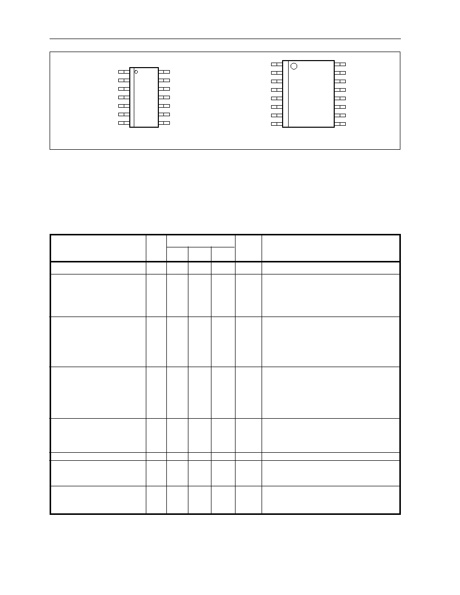
Figure 1 SP5748 Block Diagram (MP14 pinout)
and allows for coarse tuning in the up-converter application
and fine tuning in the down-converter.
Comparison frequencies are obtained either from a crystal
controlled on-chip oscillator or from an external source.
A buffered reference frequency output is also available to
drive a second SP5748. The device also contains 2 switching
ports.
-0∑3V to +7V
2∑5V
-0∑3 to V
CC
+0∑3V
-0∑3 to V
CC
+0∑3V
-0∑3 to V
CC
+0∑3V
-0∑3 to V
CC
+0∑3V
-0∑3 to V
CC
+0∑3V
-0∑3 to V
CC
+0∑3V
-0∑3 to V
CC
+0∑3V
-55
∞
C to +125
∞
C
+150
∞
C
81
∞
C/W
27
∞
C/W
2
SP5748
Datasheet
Figure 2 - Pin connections - top view
MP14
SP
5748
1
2
3
4
5
6
7
14
13
12
11
10
9
8
CHARGE PUMP
CRYSTAL CAP
CRYSTAL
ENABLE
DATA
CLOCK
PORT P1/OC
DRIVE
V
EE
RF INPUT
RFINPUT
V
CC
REF
PORTP0/OP
QP16
CHARGE PUMP
CRYSTAL CAP
CRYSTAL
ENABLE
DATA
CLOCK
PORT P1/OC
PORT P0/OP
DRIVE
V
EE
NC
RF INPUT
RF INPUT
NC
V
CC
REF
16
15
14
13
12
11
10
9
1
2
3
4
5
6
7
8
SP
5748
Electrical Characteristics
Test conditions (unless otherwise stated): Tamb = -40
∞
C to +80
∞
C, V
CC
= 4∑5V to 5∑5V. These characteristics are
guaranteed by either production test or design. They apply within the specified ambient temperature and supply
voltage ranges unless otherwise stated.
Note:
Pin numbers refer to MP14 package.
Characteristic
Conditions
Max.
Min.
Value
Typ.
Units
150MHz to 2400MHz, see Figure 6
80MHz to 150MHz, see Figure 6
See Figure 3
All input conditions
V
PIN1
= 2V, See Table 1
V
PIN1
= 2V, V
CC
= 15∑0V, T
AMB
= 25
∞
C
V
PIN14
= 0∑7V
See Figure 5 for application
Sinewave coupled via 10nF blocking capacitor
Sinewave coupled via 10nF blocking capacitor
AC coupled, see Note 1
2-20MHz
Pin
20
-400
300
300
V
CC
0∑7
10
500
±
10
20
20
0∑5
Supply current
RF input
Frequency range
Input voltage
Input impedance
Data, clock and enable
Input high voltage
Input low voltage
Input current
Hysteresis
Clock rate
Bus timing
Data set up
Data hold
Enable set up
Enable hold
Clock to enable
Charge pump
Output current
Output leakage
Drive output current
Crystal frequency
External reference
Input frequency
Drive level
Buffered reference output
Output amplitude
Output impedance
10
11,12
5,6,4
6
5,6,4
1
1
14
2,3
2
9
80
30
40
3
0
-10
300
600
300
600
300
0∑5
2
2
0∑2
13
0∑8
±
3
0∑35
250
mA
MHz
mVrms
mVrms
V
V
µ
A
Vp-p
kHz
ns
ns
ns
ns
ns
µ
A
nA
mA
MHz
MHz
Vp-p
Vp-p
cont...
3
SP5748
Datasheet
Functional description
The SP5748 contains all the elements necessary, with
the exception of a frequency reference, loop filter and
external high voltage transistor, to control a varicap tuned
local oscillator, so forming a complete PLL frequency
synthesised source. The device allows for operation with
a high comparison frequency and is fabricated in high
speed logic, which enables the generation of a loop with
excellent phase noise performance, even with high
comparison frequencies.
The block diagram is shown in Figure 1 and packages
and pin allocations in Figure 2.
The SP5748 is controlled by a standard 3-wire bus
comprising data, clock and enable inputs. The
programming word contains 26 bits, two of which are used
for port selection, 17 to set the programmable divider ratio,
4 bits to select the reference division ratio (bits RD and
R0-R2, see Table 2), two bits to set charge pump current,
bits C0 and C1 (see Table 1) and the remaining bit to
access test modes (bit T0, see Table 3)). The
programming data format is shown in Figure 4.
The clock input is disabled by an enable low signal, data
is therefore only loaded into the internal shift registers
during an enable high and is clocked into the controlling
buffers by an enable high to low transition. This load is
also synchronised with the programmable divider so giving
smooth fine tuning.
The RF signal is fed to an internal preamplifier, which
provides gain and reverse isolation from the divider
signals. The output of the preamplifier is fed to the 17-bit
fully programmable counter, which is of MN+A
architecture. The M counter is 13 bits and the A counter 4
bits.
The output of the programmable divider is fed to the phase
comparator where it is compared in both phase and
frequency domain with the comparison frequency. This
frequency is derived either from the on-chip crystal
controlled oscillator or from an external reference source.
In both cases the reference frequency is divided down to
the comparison frequency by the reference divider which
is programmable into1 of 16 ratios as described in Table 2.
The output of the phase detector feeds the charge pump
and loop amplifier section, which when used with an
external high voltage transistor and loop fiIter integrates
the current pulses into the varactor line voltage. The
charge pump current setting is described in Table 1.
A buffered crystal reference frequency suitable for driving
further synthesisers is available from pin 9. If not required
this output can be disabled by connecting to V
CC
.
The programmable divider output divided by 2, f
PD
/2 and
comparison frequency, f
COMP
, can be switched to ports
P0 and P1 respectively by switching the device into test
mode. The test modes are described in Table 3.
Electrical Characteristics
(continued)
Characteristic
At 10kHz SSB with 2MHz comparison
from 4MHz crystal
See Table 2
See Note 2
V
PORT
= 0∑7V
V
PORT
= V
CC
Conditions
Max.
Min.
Value
Units
MHz
dBc/Hz
mA
µ
A
Typ.
4
131071
320
10
2
Comparison frequency
Equivalent phase noise at
phase detector
RF division ratio
Reference division ratio
Output Ports P0 and P1
Sink current
Leakage current
Pin
7,8
NOTES
1. Reference output disabled by connecting to V
CC
.
2. Output ports high impedance on power-up, with data, clock and enable at logic `0'.
-148
240
2
4
SP5748
Datasheet
j2
j1
j0.5
j0.2
0
2
j0.2
2
j0.5
2
j1
2
j2
1
0.5
0.2
j5
2
j5
2
5
0∑5GHz
1GHz
2∑4GHz
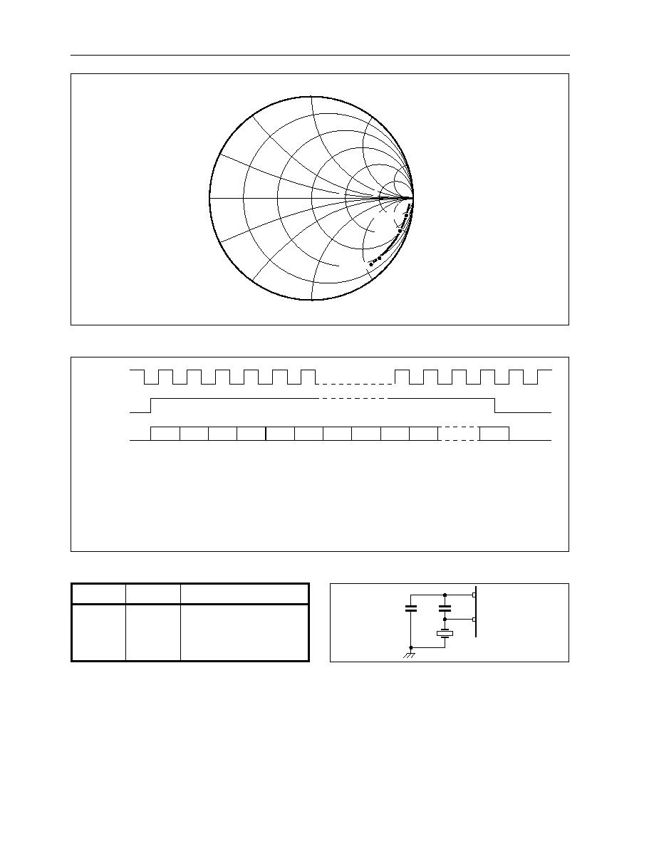
Figure 3 - RF input impedance
S11: Z
O
= 50
Normalised to 50
Figure 4 - Data format
2
25
2
24
2
23
2
22
2
21
2
20
2
19
2
18
2
17
2
16
2
0
CLOCK
ENABLE
DATA
P1
P0
T0
C1
C0
R2
R1
R0
RD
MSB
LSB
FREQUENCY
DATA
2
16
to 2
0
Programmable divider ratio control bits
R2, R1, R0 Reference divider control bits (see Table 2)
RD
Reference divider mode select (see Table 2)
P1, P0
Port control bits (see Table 3)
C1, C0
Charge pump current bits (see Table 1)
T0
Test mode enable bit
39pF
18pF
SP5748
2
3
Figure 5 - Crystal oscillator application
0
0
1
1
C1
0
1
0
1
C0
±
230
±
1000
±
115
±
500
Charge pump current (
µ
A)
Table 1 - Charge pump current

5
SP5748
Datasheet
Table 2 - Reference divider control
P1
Test mode description
X
0
0
1
1
P0
X
0
1
0
1
T0
0
1
1
1
1
Table 3 - Test modes
Normal operation
Charge pump sink
Charge pump source
Charge pump disable
Port P1= f
COMP
, P0 = f
PD
/2
Figure 7 - Example of double conversion from VHF/UHF frequencies to TV IF
SL
5748
1
2
3
4
5
6
7
14
13
12
11
10
9
8
REFERENCE
ENABLE
DATA
CLOCK
CONTROL
MICRO
39p
18p
Optional application using
on-chip crystal controlled
oscillator
68p
13.3k
15n
1n
1n
1
5V
P1
P0
22k
1
30V
BCW31
16k
47k
2.2n
TUNER
OSCILLATOR
OUTPUT
1
12V
Figure 8 - Typical application of SP5748
SP5748
2
3
10
VCO
10n
3
SP5748
1650-2400MHz
50-900MHz
1.6GHz
38.9MHz
18p
39p
80
1000
2400
FREQUENCY (MHz)
VIN (mVRMS INT
O 50
)
300
30
10
150
40
OPERATING WINDOW
Figure 6 - Typical input sensitivity
0
0
0
0
0
0
0
0
1
1
1
1
1
1
1
1
RD
0
0
0
0
1
1
1
1
0
0
0
0
1
1
1
1
R2
0
0
1
1
0
0
1
1
0
0
1
1
0
0
1
1
R1
0
1
0
1
0
1
0
1
0
1
0
1
0
1
0
1
R0
2
4
8
16
32
64
128
256
3
5
10
20
40
80
160
320
Division ratio

6
SP5748
Datasheet
Applications
A generic set of Application Notes AN168 for designing
with synthesisers such as the SP5748 has been written,
covering aspects such as loop filter design and
decoupling. This application note is published on the
Zarlink Semiconductor web site http:/www.zarlink.com. A
generic test/demonstration board has been produced
which can be used for the SP5748; the circuit diagram is
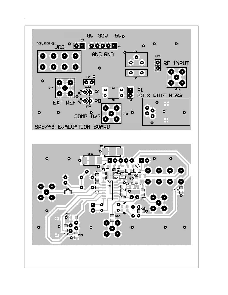
shown in Figure 9, with component values in Table 4.
The board can be used for the following purposes:
q
Measuring RF sensitivity performance.
q
Indicating port function.
q
Synthesising the voltage controlled oscillator.
q
Testing of external reference.
q
Measurement of phase noise performance.
Reference source
The SP5748 offers optimal LO phase noise performance
when operated with a large step size. This is due to the
fact that the LO phase comparator noise within the loop
bandwidth is:
+20log
10
(
LO frequency
)
Phase comparator frequency
Assuming the phase comparator noise floor is flat
irrespective of sampling frequency, this means that the
best performance will be achieved when the overall LO
There are two ways of achieving a higher phase
comparator sampling frequency:
(1) Reduce the division ratio between the reference
source and the phase comparator
(2) use a higher reference source frequency.
Approach (2) may be preferred for best performance since
it is possible that the noise floor of the reference osciliator
may degrade the phase comparator performance if the
reference division ratio is very small.
Loop bandwidth
The majority of applications for which the SP5748 is
intended require a loop filter bandwidth of between 2kHz
and10kHz.
Typically the VCO phase noise will be specified at both
1kHz and10kHz offset. It is common practice to arrange
the loop filter bandwidth such that the 1kHz figure lies
within the loop bandwidth. Thus the phase noise depends
on the synthesiser comparator noise floor, rather than
the VCO.
The 10kHz offset figure should depend on the VCO
providing the loop is designed correctly, and is not
underdamped.
Table 4 - Component values for Figure 9
C20
C21
LED 1
LED 2
R1
R4
R6
R7
R8
R9
R10
R11
R12
R13
R14
S1
T1
VCO
X1
C1
C2
C3
C4
C5
C6
C7
C8
C9
C10
C11
C12
C13
C14
C15
C16
C17
C18
C19
Component
18pF
2∑2nF
68pF
1nF
1nF
10nF
100nF
4∑7
µ
F
100nF
10pF
1nF
100pF
100pF
4∑7nF
100pF
4∑7
µ
F
10nF
39pF
100pF
Value/type
Component
1nF
1nF
HLMPK-150
HLMPK-150
4∑7k
4∑7k
13∑3k
22k
1k
0
16
16
16
68
SW DIP-2
BCW31
POS_2000
4MHz
Value/type

7
SP5748
Datasheet
Figure 9 - SP5748 evaluation board
SP
5748
1
2
3
4
5
6
7
14
13
12
11
10
9
8
D
ATA
ENABLE
CLOCK
C3
R7
C2
C5
C4
V
CC
R8
1
30V
T1
R9
R10
C14
RF3 COMP
OUTPUT
RF2
EXT REF
R1
R4
1
8V
LED1
LED2
C1
1
LK1
C17
R1
1
R12
R13
C20
1
8V
RF INPUT
RF1
C19
C21
R14
VCO
RF
OUT
VT
1
2
J2
V
ARA
CT
OR
C15
C13
C12
J5
3
4
5
6
1
2
3
4
5
1
8V
C8
C9
1
30V
C16
C7
1
5V V
CC
J1 PO
WER
CONNECT
OR
12
P1
P0
POR
T
OUTPUTS
J4
VCO tuning rang
e
= 1370MHz to 2000MHz
C18
C1
C6
LK2 is fitted f
o
r
normal operation
S1
X1
R6
LK2
8
SP5748
Datasheet
Figure 10 - SP5748 evaluation board layout
Bottom view
Top view
9
SP5748
Datasheet
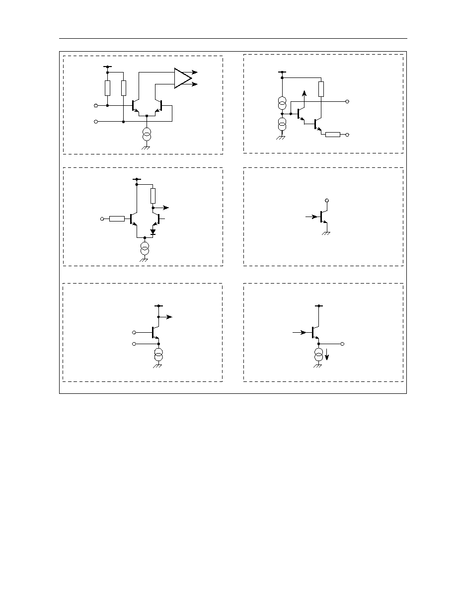
Figure 11a RF inputs
V
CC
RF
INPUTS
500
500
Figure 11b Loop amplifier
V
CC
200
CHARGE PUMP
DRIVE
Figure 11c Enable, Data and Clock inputs
V
CC
25k
Figure 11d Output ports
PORT
Figure 11e Reference oscillator
CRYSTAL
V
CC
CRYSTAL CAP
Figure 11f Reference output
REF
V
CC
1∑2mA
Figure 11 - Input/output interface circuits
c Zarlink Semiconductor 2003 All rights reserved.
APPRD.
ISSUE
DATE
ACN
Package Code
Previous package codes


www.zarlink.com
Information relating to products and services furnished herein by Zarlink Semiconductor Inc. trading as Zarlink Semiconductor or its subsidiaries (collectively
"Zarlink") is believed to be reliable. However, Zarlink assumes no liability for errors that may appear in this publication, or for liability otherwise arising from the
application or use of any such information, product or service or for any infringement of patents or other intellectual property rights owned by third parties which may
result from such application or use. Neither the supply of such information or purchase of product or service conveys any license, either express or implied, under
patents or other intellectual property rights owned by Zarlink or licensed from third parties by Zarlink, whatsoever. Purchasers of products are also hereby notified
that the use of product in certain ways or in combination with Zarlink, or non-Zarlink furnished goods or services may infringe patents or other intellectual property
rights owned by Zarlink.
This publication is issued to provide information only and (unless agreed by Zarlink in writing) may not be used, applied or reproduced for any purpose nor form part
of any order or contract nor to be regarded as a representation relating to the products or services concerned. The products, their specifications, services and other
information appearing in this publication are subject to change by Zarlink without notice. No warranty or guarantee express or implied is made regarding the
capability, performance or suitability of any product or service. Information concerning possible methods of use is provided as a guide only and does not constitute
any guarantee that such methods of use will be satisfactory in a specific piece of equipment. It is the user's responsibility to fully determine the performance and
suitability of any equipment using such information and to ensure that any publication or data used is up to date and has not been superseded. Manufacturing does
not necessarily include testing of all functions or parameters. These products are not suitable for use in any medical products whose failure to perform may result in
significant injury or death to the user. All products and materials are sold and services provided subject to Zarlink's conditions of sale which are available on request.
Purchase of Zarlink's I
2
C components conveys a licence under the Philips I
2
C Patent rights to use these components in an I
2
C System, provided that the system
conforms to the I
2
C Standard Specification as defined by Philips.
Zarlink, ZL and the Zarlink Semiconductor logo are trademarks of Zarlink Semiconductor Inc.
Copyright 2003, Zarlink Semiconductor Inc. All Rights Reserved.
TECHNICAL DOCUMENTATION - NOT FOR RESALE
For more information about all Zarlink products
visit our Web Site at