 | –≠–ª–µ–∫—Ç—Ä–æ–Ω–Ω—ã–π –∫–æ–º–ø–æ–Ω–µ–Ω—Ç: SP8607 | –°–∫–∞—á–∞—Ç—å:  PDF PDF  ZIP ZIP |

Obsolescence Notice
This product is obsolete.
This information is available for your
convenience only.
For more information on
Zarlink's obsolete products and
replacement product lists, please visit
http://products.zarlink.com/obsolete_products/

THIS DOCUMENT IS FOR MAINTENANCE
PURPOSES ONLY AND IS NOT
RECOMMENDED FOR NEW DESIGNS

DS3660-1∑2
The SP8607 is an emitter coupled logic divider which
features ECL10K compatible outputs when used with external
pulldown resistors. The inputs are AC coupled.
FEATURES
s
ECL Compatible Outputs
s
AC-Coupled Inputs (Internal Bias)
QUICK REFERENCE DATA
s
Supply Voltage: 25∑2V
s
Power Consumption: 80mW
s
Temperature Range:
2
55
∞
C to 1125
∞
C (A Grade)
2
30
∞
C to 170
∞
C (B Grade)
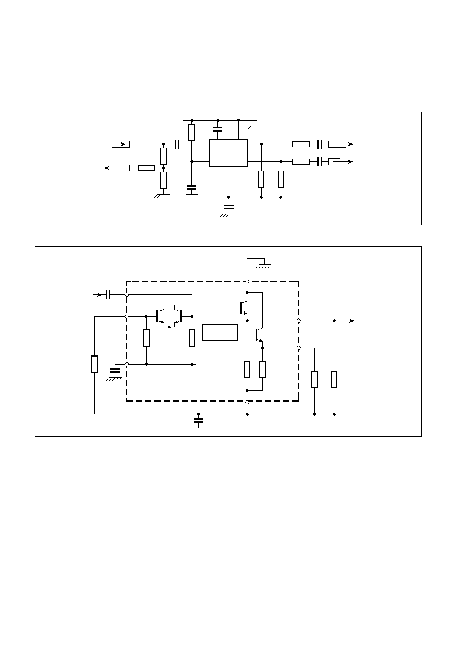
Fig. 1 Pin connections - bottom view
CM8
ORDERING INFORMATION
SP8607 A CM
SP8607 B CM
SP8607 AC CM
ABSOLUTE MAXIMUM RATINGS
Supply voltage, V
EE
Output current
Storage temperature range
Max. junction temperature
Max. clock input voltage
1
2
6
7
3
5
8
4
V
EE
(CASE)
CLOCK INPUT
OUTPUT
OUTPUT
CLOCK INPUT
V
CC
(0V)
NC
INTERNAL BIAS
DECOUPLING
SP8607
600MHz4
4
4
4
4
2
DIVIDE BY
2
V
CC
(0V)
INTERNAL BIAS
DECOUPLING
CLOCK INPUT
CLOCK INPUT
V
EE
OUTPUT
OUTPUT
3
5
6
7
1
2
8
Fig. 2 Functional diagram
2
8V
10mA
2
65
∞
C to 1150
∞
C
1
175
∞
C
2∑5V p-p
ADVANCE INFORMATION

2
SP8607
Maximum frequency (sinewave input)
Minimum frequency (sinewave input)
Power supply current
Output low voltage
Output high voltage
Minimum output swing
f
MAX
f
MIN
I
EE
V
OL
V
OH
V
OUT
600
2
1∑8
2
0∑85
400
Min.
Max.
40
18
2
1∑4
2
0∑7
Value
Notes
MHz
MHz
mA
V
V
mV
3
3
ELECTRICAL CHARACTERISTICS
Unless otherwise stated, the Electrical Characteristics are guaranteed over specified supply, frequency and temperature range
Supply voltage, V
CC
= 0V, V
EE
= 25∑2V 6 0∑25V
Temperature, T
AMB
= 255
∞
C to 1125
∞
C (A Grade), 230
∞
C to 170
∞
C (B Grade)
Units
Symbol
Characteristic
Input = 400-800mV p-p
Input = 400-800mV p-p
V
EE
= 25∑2V, outputs unloaded
V
EE
= 25∑2V
V
EE
= 25∑2V
V
EE
= 25∑2V
Conditions
NOTES
1. The temperature coefficients of V
OH
= 11∑63mV/
∞
C, and V
OL
= 10∑34mV/
∞
C but these are not tested.
2. The test configuration for dynamic testing is shown in Fig.5.
3. Tested at 25
∞
C only.
1000
800
600
400
200
0
0 100 200 300 400 500 600
INPUT FREQUENCY (MHz)
INPUT AMPLITUDE
(mV p-p)
*
Tested as specified
in table of Electrical
Characteristics
T
AMB
= 255
∞
C TO 1125
∞
C
GUARANTEED
*
OPERATING
WINDOW
Fig. 3 Typical input characteristic of SP8607A
Fig. 4 Typical input impedance. Test conditions: supply voltage = 25∑2V, ambient
temperature = 25
∞
C, frequencies in MHz, Impedances normalised to 50
100
400
200
300
500
600
j 2
j 1
j 0.5
j 0.2
0
2
j 0.2
2
j 0.5
2
j 1
2
j 2
1
0.5
0.2
j 5
2
j 5
2
5
3
SP8607
OPERATING NOTES
1. The clock inputs (pins 1 and 2) can be driven single ended or
differentially and should be capacitively coupled to the signal
source. The input signal path is completed by connecting a
capacitor from the internal bias decoupling, pin 3, to ground.
2. In the absence of a signal the device will self-oscillate. If this is
undesirable, it may be prevented by connecting a 15k
resistor
from the unused input to V
EE
. This will reduce the input sensitivity
by approximately 100mV.
3. The circuit will operate down to DC but slew rate must be better
than 100V/
µ
s.
4. The outputs are compatible with ECLII. There is an internal load
of 4k
on each output. The outputs can be interfaced to ECL10K
by the addition of 1∑5k
pulldown resistors from the outputs to V
EE
to increase output voltage swing.
5. Input impedance is a function of frequency, See Fig. 4.
6. All components should be suitable for the frequency in use.
DUT
450
450
10n
10n
OUTPUT
V
EE
5
6
7
8
2
1
1n
1n
3
3∑5k
3∑5k
33
1n
33
20
TO SAMPLING
SCOPE
GENERATOR
INPUT
1n
2∑7k
OUTPUT
Fig. 5 Test circuit
7
6
4k
4k
8
440
1
2
5
BIAS
ECL OUTPUT
1∑5k
15k
1n
1n
1n
1∑5k
V
EE
INPUT
440
DIVIDE BY
2
Fig. 6 Typical application showing interfacing