Obsolescence Notice
This product is obsolete.
This information is available for your
convenience only.
For more information on
Zarlink's obsolete products and
replacement product lists, please visit
http://products.zarlink.com/obsolete_products/
DS3675-1∑2
The SP8790 is a divide-by-four counter designed for use
with 2-modulus dividers. It increases the minimum division
ratio of the 2-modulus divider while retaining the same difference
in division ratio. The device is suitable for use in low power
frequency synthesis interfacing to CMOS or TTL.
FEATURES
s
Very Low Power
s
Control Input and Counter Output will Interface Directly
to TTL or CMOS
s
Interfaces to GPS SP8000 Series Programmable
2-Modulus Dividers
QUICK REFERENCE DATA
s
Supply Voltage: 5∑0V
s
Power Consumption: 40mW
s
Temperature Range:
2
55
∞
C to 1125
∞
C (A Grade)
2
30
∞
C to 170
∞
C (B Grade)
SP8790
60MHz4
4
4
4
4
4 (2-MODULUS EXTENDER)
1
2
6
7
3
5
8
4
V
EE
CLOCK INPUT
CONTROL OUTPUT
CLOCK INPUT
V
CC
NC
CONTROL INPUT
COUNTER OUTPUT
Fig. 1 Pin connections - bottom view
ABSOLUTE MAXIMUM RATINGS
Supply voltage
Open collector output voltage
Storage temperature range
Max. junction temperature
Max. clock input voltage
Output sink current
ORDERING INFORMATION
SP8790 A CM
SP8790 B CM
CM8
Fig. 2 Functional diagram
2
V
CC
CONTROL
OUTPUT
CLOCK INPUT
V
EE
(0V)
OPEN COLLECTOR
COUNTER OUTPUT
1
3
5
CK CK
Q
Q
D
CK CK
Q
Q
D
OUTPUT
STAGE
8
7
6
CLOCK INPUT
CONTROL
INPUT
NOTE:
NEGATIVE GOING OUTPUT
SHOULD CLOCK FOLLOWING STAGE
D
D
8V
12V
2
65
∞
C to 1150
∞
C
1
175
∞
C
2∑5V p-p
10mA
ADVANCE INFORMATION
2
SP8790
11
10
1∑5
0∑4
4∑5
3∑7
25
40
15
26
12
16
Maximum frequency (sinewave input)
Power supply current
Control input high voltage
Control input low voltage
Output high voltage (pin 3)
Output low voltage (pins 3)
Output high voltage (pin 2)
Output low voltage (pin 2)
Clock to counter output 2ve going delay
Clock to counter output 1ve going delay
Clock to control output 2ve going delay
Clock to control output 1ve going delay
Control input to control output 2ve going delay
Control input to control output 1ve going delay
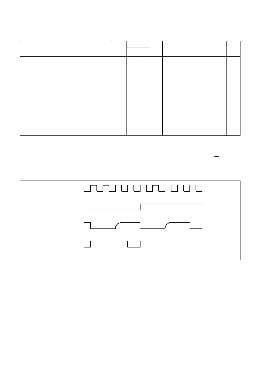
ELECTRICAL CHARACTERISTICS
Unless otherwise stated, the Electrical Characteristics are guaranteed over specified supply, frequency and temperature range
Supply voltage, V
CC
= 5V
±
0∑25V, V
EE
= 0V
Temperature, T
AMB
= 255
∞
C to 1125
∞
C (A Grade), 230
∞
C to 170
∞
C (B Grade)
Characteristic
Conditions
2
2
2
2
2
2
3
3
3, 4
3, 4
3, 4
3, 4
Notes
Tested as a controller, see Fig. 4
Pin 3 via 1∑6k
to110V
Pin 3 via 1∑6k
to110V
V
CC
= 5∑2V (25
∞
C)
V
CC
= 5∑2V (25
∞
C)
10k
pull-down on control output
10k
pull-down on control output
10k
pull-down on control output
10k
pull-down on control output
f
MAX
I
CC
V
INH
V
INL
V
OH
V
OL
V
OH
V
OL
t
pHL
t
pLH
t
pHL
t
pLH
t
pHL
t
pLH
Symbol
Units
MHz
mA
V
V
V
V
V
V
ns
ns
ns
ns
ns
ns
Min. Max.
60
3∑5
0
9
4∑27
3∑28
Value
NOTES
1. The test configuration for dynamic testing is shown in Fig.4.
2. Tested at low and high temperatures only.
3. Guaranteed but not tested.
4. The propagation delays stated are with the device controlling the SP8695, which has internal 10k
pull-down resistors on its PE inputs. These
propagation delays will be reduced when the device is used with the SP8643/47 and SP8740 series of 2-modulus dividers, which have internal
4∑3k
pull-downs. Refer to relevant data sheet/s.
CLOCK INPUT
CONTROL INPUT
COUNTER OUTPUT (PIN 3)
CONTROL OUTPUT (PIN 2)
N.B: IF CONTROL INPUT = `1' THEN CONTROL OUTPUT = `1'
Fig. 3 Timing diagram
OPERATING NOTES
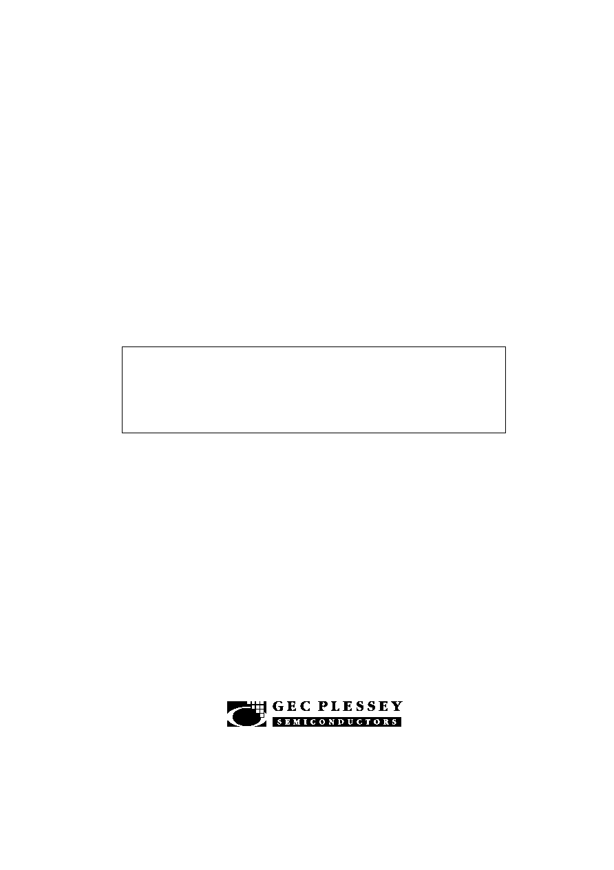
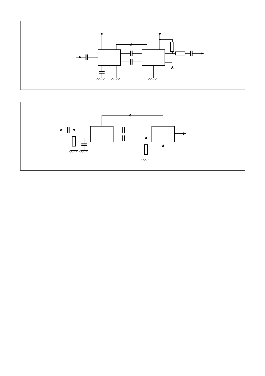
1. The device will normally be driven by capacitively coupling
the inputs to the outputs of a 2-modulus divider, as shown in
Figs. 4 and 5. The maximum frequency of the device when
used as a controller is limited by the internal delays to 60MHz.
However, when used as a 44 prescaler, it will operate at
frequencies in excess of 80MHz, the maximum frequency
being limited by saturation of the output stage.
2. The device is normally driven from very fast edges of a 2-
modulus divider, in which case there is no input slew rate
problem.
3. The control input is TTL/CMOS compatible.
4. The counter output (pin 3) interfaces to TTL/CMOS by the
addition of a pull-up resistor. For interfacing to CMOS, the
output can be connected with a pull-up resistor to a supply
which must not exceed 12V.
5. When used as a controller the device will self-oscillate in the
absence of an input signal; this can be prevented by connecting
a 47k
resistor from pin 7 to ground, as shown in Fig. 5.
6. The control output, which includes an internal 16k
pull-
down resistor, is ECL compatible and will interface directly to
ECL 2-modulus dividers such as the GPS SP8600 and SP8700
series as shown in Figs. 4 and 5.