 | –≠–ª–µ–∫—Ç—Ä–æ–Ω–Ω—ã–π –∫–æ–º–ø–æ–Ω–µ–Ω—Ç: SP8793 | –°–∫–∞—á–∞—Ç—å:  PDF PDF  ZIP ZIP |

Obsolescence Notice
This product is obsolete.
This information is available for your
convenience only.
For more information on
Zarlink's obsolete products and
replacement product lists, please visit
http://products.zarlink.com/obsolete_products/

THIS DOCUMENT IS FOR MAINTENANCE
PURPOSES ONLY AND IS NOT
RECOMMENDED FOR NEW DESIGNS
FEATURES
Very Low Power
Control Input and Output CMOS/TTL Compatible
AC Coupled Input
Operation up to 9.5V using Internal Regulator
QUICK REFERENCE DATA
Supply Voltage 5.2V or 6.8V to 9.5V
Power consumption: 26mW Typical
SP8792
225MHz
˜
80/81
SP8793
225MHz
˜
40/41
WITH ON-CHIP VOLTAGE REGULATOR
ABSOLUTE MAXIMUM RATINGS
Supply voltage
6.0V pins 7 & 8 tied
Supply voltage
13.5V pin 8, pin 7 decoupled
Storage temperature range
-55
∞
C to +125
∞
C
Max. Junction temperature
+175
∞
C
Max. clock input voltage
2.5V p-p
Vcc2 max.
10V
DS 3294- 1
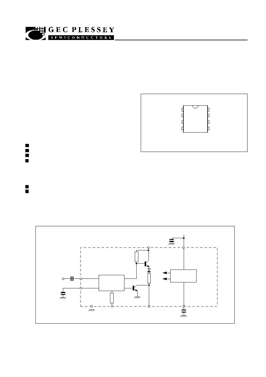
Figure 2 : Functional diagram SP8799
The SP8792 AND SP8793 are low power programmable
˜
80/81 and
˜
40/41 counter, temperature range: -40
∞
C to
+85
∞
C.They divide by 80(40) when control input is in the high
state and by 81(41) when in the low state. An internal voltage
regulator allows operation from a wide range of supply
voltages.
Figure 1 Pin connections - top view
DP8
MP8
MODULUS CONTROL INPUT
1
Vcc 1
8
OUTPUT Vcc 2
2
Vcc 2
7
OUTPUT
3
INTERNAL DECOUPLING
6
0V)
4
INPUT
5
CLOCK
INPUT
VEE (0V)
CONTROL
INPUT
OUTPUT
VCC1
100n
VCC2
1n
1n
16k
5
6
4
1
3
7
8
2
DIVIDE BY 80/81
(SP8792)
DIVIDE BY 40/41
(SP8793)
VOLTAGE
REGULATOR
100n
DECOUPLING
SP8793
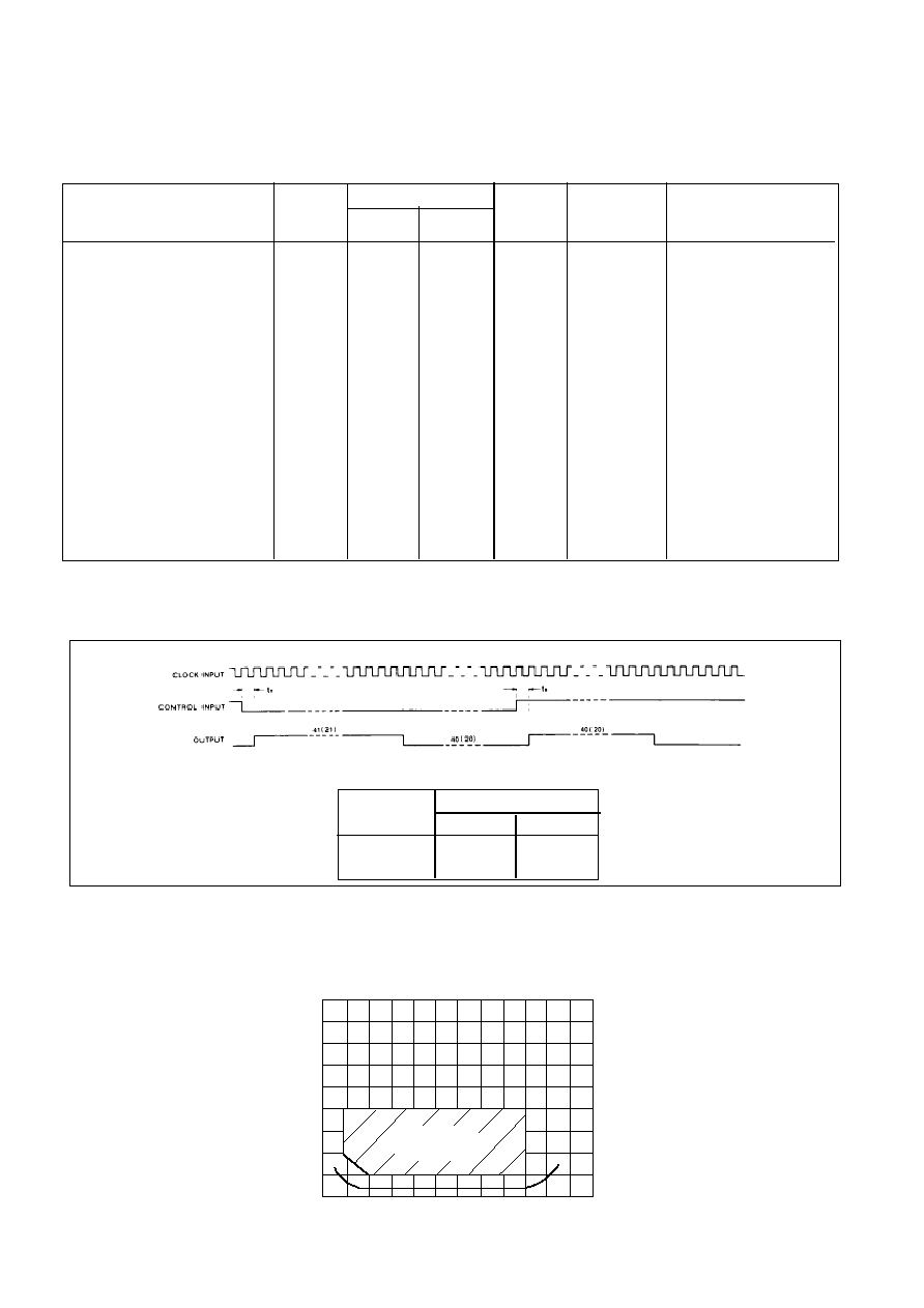
Division Ratio
SP8793
41
40
Control
inputs
0
1
SP8792
81
80
NOTES
The set-up time ts is defined as the minimum time that can elapse between a L
°
H transition of the control input and the next L
°
H clock
pulse transition to ensure
˜
80 or 40 mode is selected.
The release time tr is defined as the minimum time that can elapse between a H
°
L transition of the control input and the next L
°
H clock
pulse transition to ensure
˜
81 or 41 mode is selected.
ELECTRICAL CHARACTERISTICS
Test conditions (unless otherwise stated):]
Supply voltage : Vcc = 5.2
±
0.25V or 6.8V to 9.5V (see Operating Note 6): V
EE
= 0V
Temperature T
amb
= -40
∞
C to +85
∞
C
Conditions
Input = 200-800mV p-p
Input = 400-800mV p-p
Pins 2, 7 and 8 linked
Vcc = 4.95V I
OH
= 100
µ
A
Pin 2 linked to 8 and 7
I
OL
= 1.6mA
25
∞
C
25
∞
C
25
∞
C
Characteristics
Maximum frequency
(sinewave input))
Minimum frequency
(sinewave input)
Power supply current
Control input high voltage
Control input low voltage
Output high voltage
Output low voltage
Set up time
Release time
Clock to output propagation time
Notes
Note 4
Note 4
Note 4
Note 4
Note 4
Note 4
Note 4
Note 3
Note 3
Note 3
Units
MHz
MHz
mA
V
V
V
V
ns
ns
ns
Min.
225
4
2.4
14
20
Max.
20
7
2
0.5
45
Value
Symbol
f
max
f
min
I
EE
V
INH
V
INL
V
OH
V
OL
t
s
t
r
t
p
Figure 3 : Timing diagramSP8792/3
Figure 4 : Input sensitivity SP8792/SP8793
*Tested as specified
in table of
Electrical Characteristics
NOTES
1.
Unless otherwise stated the electrical characteristics are guaranteed over full specified supply, frequency and temperature range.
2.
The test configuration for dynamic testing is shown in Fig.6.
3.
Guaranteed but not tested.
4.
Tested onlt at 25
∞
C
TRUTH TABLE FOR CONTROL INPUTS
1600
1400
1200
1000
800
600
400
200
0
50
100
200
300
INPUT FREQUENCY (MHz)
INPUT AMPLITUDE (mV p-p)
GUARANTEED *
OPERATING
WINDOW
1800
SP8793
OPERATING NOTES
1. The clock input (Pin 5) should be capacitively coupled to
the signal source. The input signal path is completed by
coupling a capacitor from the internal bias decoupling, Pin 6 to
ground.
2. The output stage which is normally open collector (Pin 2
open circuit) can be interfaced to CMOS. The open collector
can be returned to a +10V line via a 5k resistor but the output
sink current should not exceed 2mA. If interfacing to TTL is
required then Pins 2 and 7 should be connected together to
give a fan-out = 1. This will increase supply current by
approximately 2mA.
3. The circuit will operate down to DC but a slew rate of better
than 20V/~s is required.
4. The mark space ratio of the output is approximately 1.2:1
at 200MHz.
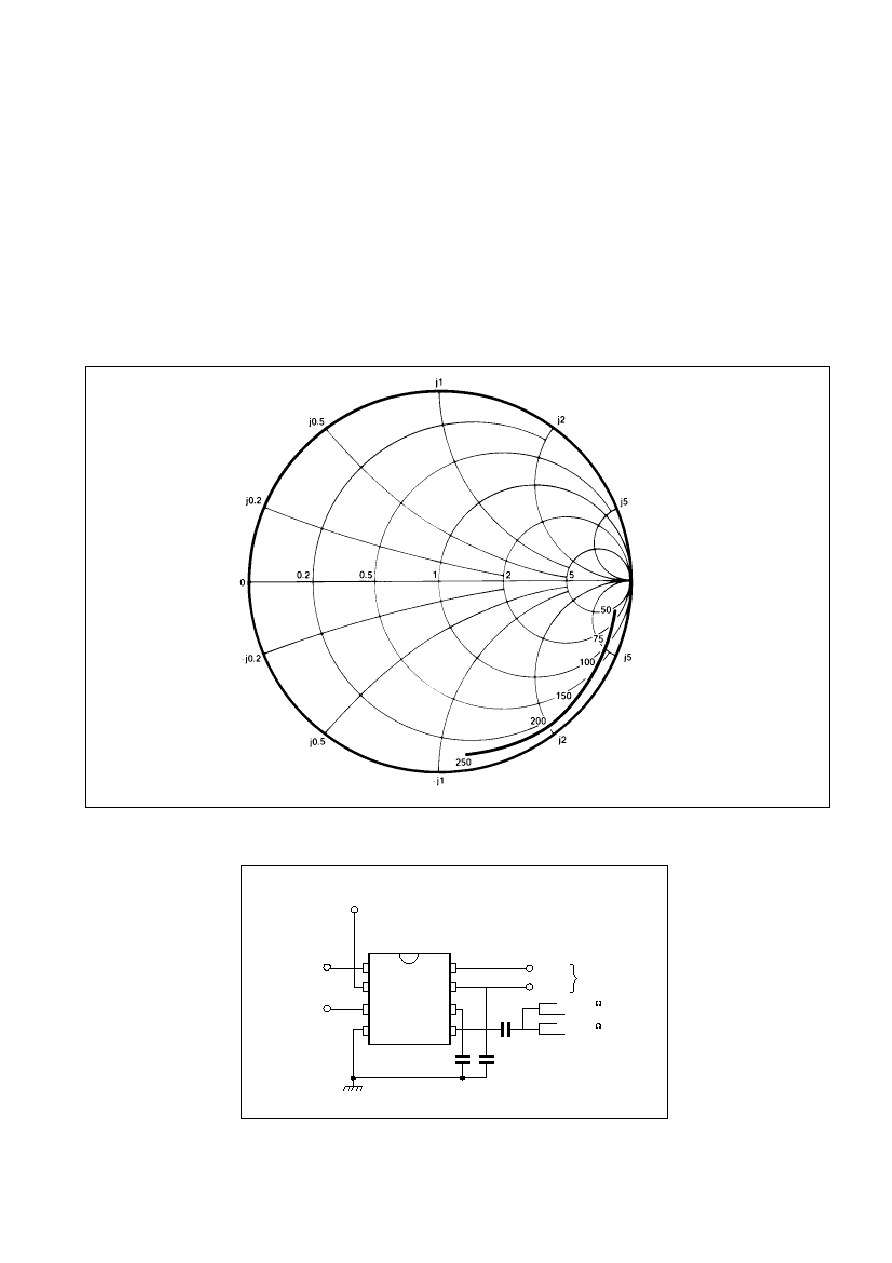
5. Input impedance is a function of frequency. See Fig.5.
6. If no signal is present the device will self-oscillate. If this is
undesirable it may be prevented by connecting a 150k
between unused input and ground. This reduces the input
sensitivity by typically 50-100mV p-p.
7. The internal regulator has its input connected to Pin 8,
while the internal reference voltage appears at Pin 7 and
should be decoupled. For use from a 5.2V supply, Pins 7 and
8
should be connected together, and 5.2V applied to these
pins. For operation from supply voltages in the range +6.8V to
+9.5V, Pins 7 and 8 should be separately decoupled, and the
supply voltage applied to Pin 8.
Figure 5 : Typical impedance. Test conditions: supply voltage 5.2V, ambient temperature 25
∞
C, frequencies in
MHz, impedance normalised to 50 ohms.
Figure 6 : Toggle frequency test circuit
1
8
2
7
3
6
4
5
VCC1
CONTROL
INPUT
OUTPUT
VCC OF MODULUS
CONTROL DEVICE
1n
100n
1n
50
MONITOR
50
SIGNAL
SOURCE
VCC2
SEE OPERATING
NOTE 6