SP8853
1.3 GHz Professional Synthesiser
The SP8853 is a low power single chip synthesiser
intended for professional radio applications, containing all the
elements (apart from the loop amplifier) required to build a PLL
frequency synthesis loop
The device is serially programmable by a three-wire data
highway and contains three independent buffers to store one
reference divider word and two local oscillator divider words.
A digital phase detector with two charge pumps,
programmable in phase and gain, are provided to improve
lock-up performance. The preset operation of the charge
pumps can be overwritten or the comparison frequencies
switched to output ports under control of the divider word. The
dual modulus ratio and so operating range is also
programmable through the same word.
A power down mode is incorporated as a battery economy
feature.
The SP8853 is specified at 1.3GHz at -55∞C to +125∞C (mil
temp) and -40∞C to +85∞C (ind. temp).
June 2003
FEATURES
s
Improved Digital Phase Detector Eliminates
`Dead Band' Effects
s
Low Operating Power, Typically 175mW
s
1∑3GHz Operating Frequency
s
Complete Phase Locked Loop
s
High Input Sensitivity
s
Programmed throughThree-Wire Bus
s
Wide Range of Reference Division Ratios
s
Local Storage for Two Frequency Words, giving
Rapid Frequency Toggling
s
Programmable Phase Detector Gain
s
Power Down Mode
ABSOLUTE MAXIMUM RATINGS
Supply voltage
Storage temperature
Prescaler input voltage
2
0∑3V to 17V
2
55
∞
C to 1150
∞
C
2∑5V p-p
Fig. 1 Pin identification diagram (top view)
ORDERING INFORMATION
SP8853/A/DG, SP8853/A/HC Industrial temperature versions
SP8853/AC/DG, SP8853/AC/HC Military temperature versions
4
3
2
1
28
27
26
12
13
14
15
16
17
18
5
6
7
8
9
10
11
25
24
23
22
21
20
19
PD2 OUTPUT
RPD
V
CC
3
GROUND
XTAL 1
XTAL2
V
EE
2
F
REF
*
POWER DOWN
V
EE
4
V
CC
4
V
CC
1
RF INPUT
RF INPUT
F
PD
*
PD1 OUTPUT
V
EE
3
IC
Cd
LOCK DETECT
NC
V
EE
1
F1/F2
D
ATA
CLOCK
ENABLE
NC
V
CC
2
SP8853
HC28
*F
PD
and F
REF
outputs are reversed by the phase
detector sense bit in the F1/F2 programming word. The
above diagram is correct when the sense bit is low. See
Table 2 and Fig. 7.
V
CC
1, V
EE
1 ≠ preamplifier and prescaler supplies
V
CC
2, V
EE
2 ≠ oscillator supplies
V
CC
3, V
EE
3 ≠ charge pump 2 supplies
V
CC
4, V
EE
4 ≠ ECL supplies
Data Sheet
SP8853
1.3 GHz Professional Synthesiser
5
SP8853
DESCRIPTION
Prescaler and AM Counter
The programmable divider chain is of
AM counter design
and therefore contains a dual modulus front end prescaler, an
A counter which controls the dual modulus ratio and an M
counter which controls the bulk multi-modulus division.
A programmable divider of this type has a division ratio of
MN
1
A and a minimum integer steppable division ratio
of
N(N
2
1).
In the SP8853, the dual modulus front end prescaler is a
dual
N ratio device, capable of being statically switched
between
4
16/17 and
4
8/9 ratios. The controlling
A counter is
of four-bit design, allowing a maximum count sequence of 15
(2
4
2
1), which begins with the start of the
M counter sequence
and stops when it has counted by the pre-loaded number of
cycles. While the A counter is counting, the dual modulus
prescaler is held in the
N
1
1 mode then reverts to the
N mode
at the completion of the sequence.
The
M counter is a 15-bit asynchronous divider which
counts with a ratio set by a control word. In both
A and M
counters the controlling data from the F1/F2 buffer is loaded
in sequence with every
M count cycle. The N ratio of the dual
modulus prescaler is selected by a one-bit word in the
reference divider buffer and, when when a ratio of
4
8/9 is
selected, the A counter requires only three programming bits,
having an impact on the frequency bit allocation as described
in the data entry section.
Reference Source and Divider
The reference source in the SP8853 is obtained from an
on-chip oscillator which is frequency controlled by an external
crystal. The oscillator can also function as a buffer amplifier to
allow the use of an external reference source. In this mode, the
source is simply AC-coupled into the oscillator transistor base
on pin 20.
The oscillator output is coupled to a programmable reference
counter (
R) whose output is the reference for the phase
detector. The reference divider is a fully programmable 13-bit
asynchronous design and can be set to any division ratio
between 1 and 8191. The actual division ratio is controlled by
a data word stored in the internal reference buffer.
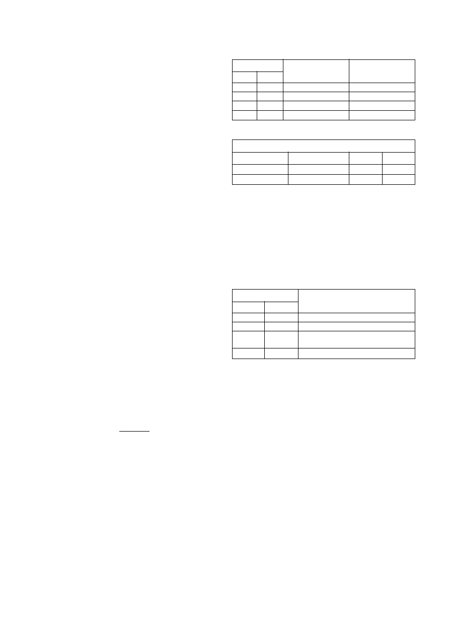
Phase Detector
The SP8853 contains a digital phase detector which feeds
two charge pump circuits. Charge pump 1 has preset currents
which are programmble as shown in Table 1. Charge pump 2
has a current level set by an external resistor RPD; the current
is multiplied by a factor which is determined by bits G1 and G2
of the F1 or F2 word (see Table 1). Note that charge pump 2
current is pin 24 current
3
muliplication factor, where
I pin 24 =
A lock detect circuit is connected to the output of charge
pump 2. when the voltage level at pin 25 is between
approximately 2∑25V and 2∑75V, LOCK DETECT (pin 27) will
be low and charge pump 1 disabled, depending on the PD1
and PD2 programming bits as shown in Table 4.
The output signals from the
R and M counters are available
on pins 4 and 5 (F
PD
and F
REF
) when programmed by the
reference programming word; the various options are shown
in Table 4. An external phase detector may be connected to
pins 4 and 5 and may be used independently or in conjunction
with the on-chip phase detector.
To allow for control direction changes introduced by the
design of the control loop, a control bit in the F1/F2 programming
word interchanges the inputs to the on-chip phase detector
and reverses the functions on pins 4 and 5 (see Table 2).
V
CC
2
1∑5V
RPD
F1 or F2 word
G2 G1
Charge pump 1
current (
µ
A)
Charge pump 2
multiplier
0
1
Current source
Current sink
F
PD
F
REF
F1/F2 sense bit
Pins 3 and 25
Pin 4
Output for RF phase lag
F
REF
F
PD
Pin 5
0
1
0
1
0
0
1
1
50
75
125
200
1
1∑5
2∑5
4
Table 1 Charge pump currents
Table 2
Data Entry and Storage
The data section of the SP8853 consists of a data input
interface, a data shift register and three data buffers.
Data is entered to the data input interface via a three-wire
highway, with DATA (pin 24), CLOCK (pin 15) and ENABLE
(pin16) inputs. The input interface routes the data into a 24-
bit shift register with bus connections to three data buffers.
Data entered via the serial bus is transferred to the appropriate
data buffer on the negative transition of the data enable input
according to the two final data bits C1 and C2 as shown in
Table 3. The MSB of the data is entered first.
2-bit SR contents
C2 C1
0
1
0
1
F1
F2
Transfer A counter bits (N0:N3)
into 4-bit buffer (see Figs. 2 and 7)
Reference
0
0
1
1
Buffer loaded
Table 3
The dual F1/F2 buffer can receive two 22-bit words and
controls the programmable divider A and M counters using 19
bits, the phase detector gain with two bits and the phase
detector sense with one bit. A fourth input from the synthesiser
control system selects the active buffer.
The third buffer contains only 16 bits, 13 being used to set
the reference divider division ratio and 2 to control the phase
detector enable logic. The remaining bit sets the dual modulus
prescaler
N ratio.
The data words may be entered in any individual multiple
sequence and the shift register can be updated whils the data
buffers retain control of the synthesiser with the previously
loaded data. This enables four unique data words to be stored
in the device, with three in the data buffers and a fourth in the
shift register, while the chip is enabled. The F1 word may also
be updated while F2 is controlling the programmable divider
and vice-versa.
The dual F1/F2 buffer enables allows the device to be
toggled between two frequencies using the F1/F2 select input
at a rate determined by the comparison frequency and also
permits random frequency hopping at a rate determined by a
btye load period; this is possible because the loop can be
locked to F1 while F2 is updated by entering new data via the
shift register. The F1/F2 input is high to select F1.
Data Sheet