HC44
SP8854E
2.7GHz Parallel Load Professional Synthesiser
Preliminary Information
DS4238
ISSUE 2.0
June 1998
Ordering Information
SP8854E KG HCAR
Non-standard temperature range,
255
∞C to 1100∞C, standard product screening
SP8854E IG HCAR
Industrial temperature range,
240
∞C to 185∞C, standard product screening
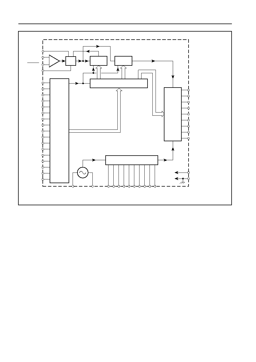
The SP8854E is one of a family of parallel load synthesisers
containing all the elements apart from the loop amplifier to
fabricate a PLL synthesis loop. Other parts in the series are
the SP8852E which is fully programmable, requiring tw0 16-
bit words to set the RF and reference counters and the
SP8855E which is fully programmable using hard wired links
or switches.
The SP8854E is programmed using a 16-bit parallel data
bus. Data is stored in an internal buffer. The 10-bit program-
mable reference divider is programmed by connecting the
10 programming pins either to ground or 15V. The device
can therefore be programmed with a single transfer from the
control microprocessor. Hard wired inputs can also control
the F
PD
and F
REF
outputs and the control sense of the loop.
Features
∑
2∑7 GHz Operating Frequency
∑
Single 5V Supply
∑
Low Power Consumption <1∑3W
∑
High Comparison Frequency : 20MHz
∑
High Gain Phase Detector : 1mA/rad
∑
Zero `Dead Band' Phase Detector
∑
Wide Range of RF and Reference Division Ratios
∑
Programming by Single Word Data Transfer
Absolute Maximum Ratings
Supply voltage
Operating temperature
Storage temperature
Prescaler and reference input voltage
Data inputs
Junction temperature
20∑3V to 16V
255
∞C to1100∞C
265
∞C to 1150∞C
2∑5V p-p
V
CC
10∑3V
V
EE
20∑3V
1175
∞C
Figure 1 - Pin connections - top view
*F
PD
and F
REF
outputs are reversed using the control
direction input, pin 23. The above diagram is correct
when pin 23 is high.
1 44
DATA BIT 4
DATA BIT 3
DATA BIT 2
DATA BIT 1
DATA BIT 0
0V (PRESCALER)
RF INPUT
RF INPUT
V
CC
(PRESCALER)
VEE
LOCK DETECT
STROBE
REF DIV BIT 0
REF DIV BIT 1
REF DIV BIT 2
REF DIV BIT 3
REF DIV BIT 4
REF DIV BIT 5
REF DIV BIT 6
REF DIV BIT 7
REF DIV BIT 8
REF DIV BIT 9
C-LOCK DETECT
R
SET
CHARGE PUMP
OUTPUT
CHARGE PUMP
REF
F
PD
/F
REF
ENABLE
CONTROL
DIRECTION
F
PD
*
F
REF
*
V
CC
REF OSC CAP
ACIT
OR
REF IN/CR
YST
AL
DA
T
A
BIT 5
DA
T
A
BIT 6
DA
T
A
BIT 7
DA
T
A
BIT 8
DA
T
A
BIT 9
DA
T
A
BIT 10
DA
T
A
BIT 1
1
DA
T
A
BIT 12
DA
T
A
BIT 13
DA
T
A
BIT 14
DA
T
A
BIT 15
SP8854E
2
SP8854E
Preliminary Information
STROBE
B0
B1
B2
B3
B4
B5
B6
B7
B8
B9
B10
B11
B12
B13
B14
B15
39
11
10
9
8
7
6
5
4
3
2
1
44
43
42
41
40
INPUT
INTERFACE
48/9
13
14
15
14
V
CC
PRESCALER
RF INPUT
0V
PRESCALER
3-BIT
A COUNTER
11-BIT
M COUNTER
B0
B2
B3
B13 B14
B15
LOAD
RF BUFFER
PHASE
DETECTOR
10-BIT REFERENCE DIVIDER
F
REF
F
PD
REFERENCE
CRYSTAL
REFERENCE
CAPACITOR
28
27
CHARGE PUMP OUTPUT
CHARGE PUMP REFERENCE
LOCK DETECT OUTPUT
R
SET
C-LOCK DETECT
F
PD
*
F
REF
*
FPD/FREF ENABLE
CONTROL DIRECTION
V
CC
V
EE
MODULUS
CONTROL
*FREF and FPD outputs are reversed using
the control direction input. The pin allocations
shown are correct when bit 12 is high.
20
21
17
19
18
24
25
22
23
26
16
RF INPUT
BIT 0
38
37
36
35
34
33
32
31
30
29
BIT 9
REFERENCE DIVIDER PROGRAMMING
Figure 2 - Block Diagram

3
SP8854E
Preliminary Information
Pin
Description
These pins are the data inputs to set the RF divider ratio (MN1A). High is open circuit on these
pins. Data is transparent from pins to RF buffer when pin 39 (STROBE) is high and frozen in
buffers when pin 39 is low.
Balanced inputs to the RF preamplifier. For single-ended operation the signal is AC-coupled into
pin 13 with pin 14 AC-decoupled to ground (or vice-versa). Pins 13 and 14 are internally DC
biased.
A current sink into this pin is enabled when the lock detect circuit indicates lock. Used to give
an external indication of phase lock.
A capacitor connected to this point determines the lock detect integrator time constant and can
be used to vary the sensitivity of the phase lock indicator.
An external resistor from pin 19 to V
CC
sets the charge pump output current.
The phase detector output is a single ended charge pump sourcing or sinking current to the
inverting input of an external loop filter.
Connected to the non-inverting input of the loop filter to set the optimum DC bias.
Part of the input bus. When this pin is high, the F
REF
/ F
PD
outputs are enabled.
High is open circuit.
This pin controls charge pump output direction. When pin 23 is high, the output sinks current
when F
PD
> F
REF
or when the RF phase leads the reference phase. When pin 23 is low, the
relationship is reversed (see Table 3).
RF divider output pulses. F
PD
= RF input frequency/(M.N1A). Pulse width = 8 RF input cycles
(1 cycle of the divide by 8 prescaler output).
Reference divider output pulses. F
REF
= reference input frequency/R. Pulse width = high period
of Ref input.
Leave open circuit if an external reference is used. See Fig. 5 for typical connection for use as
an onboard crystal oscillator.
This pin is the input buffer amplifier for an external reference signal. This amplifier provides the
active element if an onboard crystal oscillator is used.
These pins set the reference divider ratio R. High is open circuit.
When pin 39 is high the A, M, and R counters are held in the reset state and the charge pump
output is disabled. When pin 39 is low the data on the RF data and PD gain pins is fixed in the
buffers, the buffers are loaded into the RF counters and the PD gain control, all the counters are
active, and the charge pump is enabled. High is open circuit.
These pins set the charhe pump current multiplication factor (see Table 2). The data is
transparent into the buffers when pin 39 is high and frozen when pin 39 is low.
High is open circuit.
1-11, 42-44
13 (RF INPUT)
14 (RF INPUT)
17 (LOCK DETECT INPUT)
18 (C-LOCK DETECT)
19 (R
SET
)
20 (CHARGE PUMP OUTPUT)
21 (CHARGE PUMP REF)
22 (F
REF
/ F
PD
ENABLE)
23 (CONTROL DIRECTION)
24
F
PD
if pin 23 is high
F
REF
if pin 23 is low
25
F
PD
if pin 23 is low
F
REF
if pin 23 is high
27 (Ref. oscillator capacitor)
28 (REF IN/XTAL)
29-38
39 (STROBE)
40, 41 (PD gain)
Table 1 - Pin Descriptions

4
SP8854E
Preliminary Information
Supply current
RF input sensitivity
RF division ratio
Reference division ratio
Comparison frequency
Reference input frequency
Reference input voltage
F
REF
/F
PD
output voltage high
F
REF
/F
PD
output voltage low
LOCK DETECT output voltage
CHARGE PUMP current
Input bus logic level high
Input bus logic level low
Input bus current source
Input bus current sink
Up/down current matching
CHARGE PUMP REFERENCE voltage
R
SET
current
R
SET
voltage
C-LOCK DETECT current
STROBE pulse width
Data setup time
Electrical Characteristics
The Electrical Characteristics are guaranteed over the following range of operating conditions unless otherwise stated
T
AMB
= 2 55
∞C to 1100∞C (KG parts), 2 40∞C to 185∞C (IG parts); V
CC
= 4∑75V to 5∑25V
Characteristic
Conditions
25
56
1
10
0
61∑4
62∑0
63∑4
65∑4
3∑5
2200
V
CC
21∑6
0∑5
50
100
180
16
20∑8
21∑4
300
61∑5
62∑3
63∑8
66∑1
1∑6
110
Pin
18, 26
13,14
13,14, 24
28, 25
28, 24, 25
28
28
24, 25
24, 25
17
19, 20, 21
1-11, 22,
23, 29, 44
1-11, 22,
23, 29, 44
1-11, 22,
23, 29, 44
1-11, 22,
23, 29, 44
20
21
19
19
18
Typ.
Max.
Min.
mA
dBm
MHz
MHz
dBm
V
V
mV
mA
mA
mA
mA
V
V
µA
µA
%
V
V
mA
V
µA
ns
ns
Units
Value
240
17
16383
1023
50
100
110
500
61∑7
62∑5
64∑1
66∑5
1
10
65
V
CC
20∑5
2
100MHz to 2∑7GHz. See note 3.
Ref division ratio >2. See note 1
WRT V
CC
, 2∑2k
to 0V
WRT V
CC
, 2∑2k
to 0V
I
OUT
= 3mA
V
PIN20
= V
PIN21
, I
PIN19
= 1∑6mA,
multiplication factor = 1
V
PIN20
= V
PIN21
, I
PIN19
= 1∑6mA,
multiplication factor = 1∑5
V
PIN20
= V
PIN21
, I
PIN19
= 1∑6mA,
multiplication factor = 2∑5
V
PIN20
= V
PIN21
, I
PIN19
= 1∑6mA,
multiplication factor = 4∑0
V
IN
= 0V
V
IN
= V
CC
V
PIN20
= V
PIN21
, I
PIN19
= 1∑6mA
I
PIN19
= 1∑6mA, current
multiplication factor = 1∑0
I
PIN19
= 1∑6mA, current
multiplication factor = 4∑0
Note 2
I
PIN19
= 1∑6mA
V
PIN18
= 4∑7V
Note 3
Note 3
NOTES
1. Lower frequencies may be used provided that slew rates are maintained.
2. Pin 19 current3multiplication factor must be less than 5mA if charge pump accuracy is to be maintained.
3. Guranteed but not tested.
5
SP8854E
Preliminary Information
120
110
17
0
25
210
220
230
100MHz
FREQUENCY
RF INPUT T
O
PIN 13 (dBm)
1GHz
2GHz 2∑7GHz
10GHz
GUARANTEED
OPERATING WINDOW
TYPICAL SENSITIVITY
TYPICAL OVERLOAD
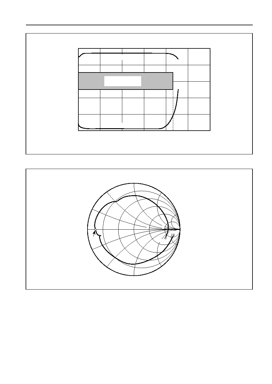
Figure 3 - Input sensitivity
1∑1GHz
Z
O
= 50
j 2
j 1
j 0.5
j 0.2
0
2j 0.2
2j 0.5
2j 1
2j 2
1
0.5
0.2
j 5
2j 5
2
5
2∑5GHz
50MHz
Figure 4 - RF input impedance