
Obsolescence Notice
This product is obsolete.
This information is available for your
convenience only.
For more information on
Zarlink's obsolete products and
replacement product lists, please visit
http://products.zarlink.com/obsolete_products/

SP8855D
12
PACKAGE DETAILS
Dimensions are shown thus: mm (in). For further package information please contact your local Customer Service Centre.
INDEX CORNER
17.27/17.78
(0.680/0.700)
16.33/16.81
(0.643/0.662)
1.27/(0.050) NOM
1.02MM/(0.040
I
)NOM
45
∞
AT 3 PLACES
0.51 (0.02) NOM
AT 45
∞
16.33/16.81
(0.643/0.662)
17.27/17.78
(0.680/0.700)
12.45/12.95
(0.490/0.510)
12.45/12.95
(0.490/0.510)
15.49/16.51
(0.610/0.650)
0.76MM(0.030
)
0.43MM(0.017
)
0.89(0.035)
03.05/3.43
(0.120/0.135)
HC44 MULTILAYER CERAMIC J LEADED CHIP CARRIER
HEADQUARTERS OPERATIONS
GEC PLESSEY SEMICONDUCTORS
Cheney Manor, Swindon,
Wiltshire United Kingdom SN2 2QW.
Tel: (01793) 518000
Fax: (01793) 518411
GEC PLESSEY SEMICONDUCTORS
P.O. Box 660017 1500 Green Hills Road,
Scotts Valley, California 95067≠0017,
United States of America. Tel: (408) 438 2900
Fax: (408) 438 5576
This publication is issued to provide information only, which (unless agreed by the Company in writing) may not be used, applied or reproduced for any purpose nor form part of any
order or contract nor to be regarded as a representation relating to the products or services concerned. No warranty or guarantee express or implied is made regarding the capability,
performance or suitability of any product or service. The Company reserves the right to alter without prior notice the specification, design, or price of any product or service. Information
concerning possible methods of use is provided as a guide only and does not constitute any guarantee that such methods of use will be satisfactory in a specific piece of equipment. It
is the user's responsibility to fully determine the performance and suitability of any equipment using such information and to ensure that any publication or data used is up to date and
has not been superseded. These products are not suitable for use in any medical products whose failure to perform may result in significant injury or death to the user. All products and
materials are sold and services provided subject to the Company's conditions of sale, which are available on request.
E
GEC Plessey Semiconductors 1995 Publication No. D.S. 3702 Issue No. 2.6 October 1995
CUSTOMER SERVICE CENTRES
F
FRANCE & BENELUX Les Ulis Cedex Tel: (1) 64 46 23 45
Fax: (1) 69 18 90 00
F
GERMANY Munich Tel: (089) 3609 06 0 Fax: (089) 3609 06 55
F
ITALY Milan Tel: (02) 66040867 Fax: (02) 66040993
F
JAPAN Tokyo Tel: (03) 5276≠5501 Fax: (03) 5276≠5510
F
NORTH AMERICA Scotts Valley, USA
Tel: (408) 438 2900 Fax: (408) 438 7023
F
SOUTH EAST ASIA Singapore Tel: (65) 3827708 Fax: (65) 3828872
F
SWEDEN Stockholm Tel: 46 8 7029770 Fax: 46 8 6404736
F
TAIWAN, ROC Taipei Tel: 886 2 5461260 Fax: 886 2 7190260
F
UK, EIRE, DENMARK, FINLAND & NORWAY
Swindon Tel: (01793) 518527/518566 Fax: (01793) 518582
These are supported by Agents and Distributors in major countries world≠wide.
TECHNICAL DOCUMENTATION ≠ NOT FOR RESALE. PRINTED IN UNITED KINGDOM
SP8855D
11
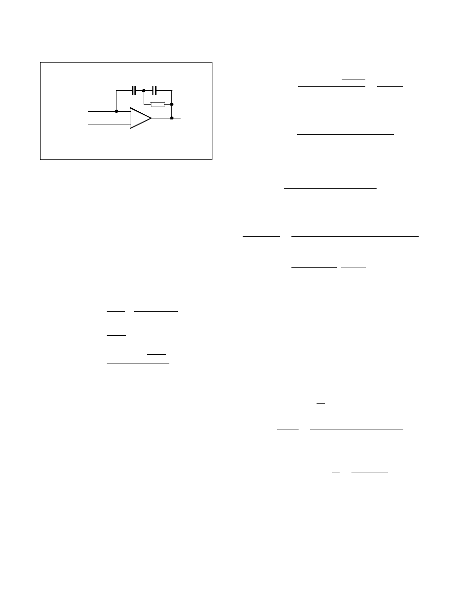
FROM
CHARGE
PUMP
REFERENCE
C
1
C
2
R
2
TO
VCO
FROM
CHARGE
PUMP
OUTPUT
Fig. 8 Third order loop filter circuit diagram
≠
+
Loop Filter Design
Generally the third order filter configuration shown in Fig.7
gives better results than the more commonly used second
order because the reference sidebands are reduced. Three
equations are required to determine values for the three
constants where;
t
1
= C
1
t
2
= R
2
(C
1
+ C
2
)
t
3
= C
2
R
2
The equations are;
1
t
2
+
1
w
n
2
t
3
2
t
3
+
*
tan
F
0
)
1
cos
F
0
w
n
3
t
1
+
K
f
K
0
N
w
n
2
1
) w
n
2
t
2
2
1
) w
n
2
t
3
2
Ω
Where;
K
f
is the phase detector gain factor in mA/radian
K
0
is the VCO gain factor in radian/second/Volt
N
is the total division ratio from VCO to reference
frequency
w
n
is the natural loop bandwidth
F
0
is the phase margin normally set to 45
∞
Since the phase detector is linear over a range of 2
p
radian,
K
f
can be calculated from
K
f
= Phase comparator current setting/2
p
mA/radian
These values can now be substituted in equation 1 to obtain
a value for C
1
and equation 2 and 3 used to determine values
for C
2
and R
2
EXAMPLE
Calculate values for a loop with the following parameters
Frequency to be synthesised:
1000MHz
Reference frequency
10MHz
Division ratio
1000MHz/10MHz = 100
w
n
natural loop frequency
100kHz
K
0
VCO gain factor
2
p
x 10MHz/Volt
F
0
phase margin
45
∞
Phase comparator current
6.3mA
The phase detector gain factor K
f
= 6.3mA /2
p
= 1mA/radian
From equation 3:
t
3
+
*
tan 45
∞
)
1
cos 45
∞
100kHz
2
p
+
0 . 4142
628319
From equation 2:
t
2
+
1
(100kHz
2
p
)
2
659
10
*
9
t
2
+
3 . 844
10
*
6
Using these values in equation 1:
t
1
+
1 x 10
*
3
2
p
10MHz V
100
(2
p
100kHz)
2
[
A
]
Ω
t
3
+
659
10
*
9
Where A is :
t
1
+
1 . 59
10
*
9
x 2 . 415
t
1
+
3 . 84
10
*
9
Now
t
1
+
C
1
N
C
1
+
3 . 84nF
t
2
+
R
2
(C
1
)
C
2
)
t
3
+
C
2
R
2
t
1
+
62832
39 . 48 10
12
6 . 833
1 . 1714
Ω
1
) w
n
2
t
2
2
1
) w
n
2
t
3
2
+ 1 )
(2
p
100k
Hz
)
2
(3 . 844 x 10
*
6
)
2
1
)
(2
p
100k
Hz
)
2
(659 x 10
*
9
)
2
Substituting for C
2
t
2
+ R
2
C
1
)
t
3
R
2
N t
2
+
R
2
C
1
) t
3
N
R
2
+
t
2
* t
3
C
1
+
3 . 844 10
*6
* 659 10
*9
9 . 61 10
*9
R
2
+
829
. 4W
t
3
+ C
2
R
2
N C
2
+
t
3
R
2
+
659 10
*9
829 . 4
C
2
+
0 . 794
nF

SP8855D
10
gain can be modified when new frequency data is entered to
compensate for change in the VCO gain characteristic over its
frequency band. The charge pump pulse current is
determined by the current fed into pin 19 and is approximately
equal to pin 19 current when the programmed multiplication
ratio is one. The circuit diagram Fig. 7e shows the internal
components on pin 19 which mirror the input current into the
charge pump. The voltage at pin 19 will be approximately 1.6V
above ground due to two V
be
drops in the current mirror. this
voltage will exhibit a negative temperature coefficient, causing
the charge pump current to change with chip temperature by
up to 10% over the full military temperature range if the current
programming resistor is connected to V
CC
as shown in the
application diagram Fig. 5. In critical applications where this
change in charge pump current would be too large the resistor
to pin 19 could be increased in value and connected to a
higher supply to reduce the effect of V
be
variation on the
current level. A suitable resistor connected to a 30V supply
would reduce the variation in pin 19 current due to
temperature to less than 1.5%. Alternatively a stable current
source could be used to set pin 19 current.
The charge pump output on pin 20 will only produce
symmetrical up and down currents if the voltage is equal to that
on the voltage reference pin 21. In order to ensure that this
voltage relationship is maintained, an operational amplifier
must be used as shown in the typical application Fig. 5. Using
this configuration pin 20 voltage will be forced to be equal to
that on pin 21 since the operational amplifier differential input
voltage will be no more than a few millivolts (the input offset
voltage of the amplifier). When the synthesiser is first switched
on or when a frequency outside the VCO range is programmed
the amplifier output will limit, allowing pin 20 voltage to differ
from that on pin 21. As soon as an achievable frequency value
is programmed and the amplifier output starts to slew the
correct voltage relationship between pin 20 and 21 will be
restored. Because of the importance of voltage equality
between the charge pump reference and output pins, a
resistor should never be connected in series with the
operational amplifier inverting input and pin 20 as is the case
with a phase detector giving voltage outputs. Any current
drawn from the charge pump reference pin should be limited
to the few micro amps input current of a typical operational
amplifier. A resistor between the charge pump reference and
the non inverting input could be added to provide isolation but
the value should not be so high that more than a few millivolts
drop are produced by the amplifier input current.
When selecting a suitable amplifer for the loop filter, a
number of parameters are important; input offset voltage in
most designs is only a few milivolts and an offset of 5mV will
produce a mismatch in the up and down currents of about 4%
with the charge pump multiplication factor set at 1. The
mismatch in up down currents caused by input offset voltage
will be reduced in proportion to the charge pump multiplication
factor in use. If the linearity of the phase detector about the
normal phase locked operating point is critical, the input offset
voltage of most amplifiers can be adjusted to near zero by
means of a potentiometer.
The charge pump reference voltage on pin 21 is about 1.3V
below the positive supply and will change with temperature
and with the programmed charge pump multiplication factor.
In many cases it is convenient to operate the amplifier with the
negative power supply pin connected to 0V as this removes
the need for an additional power supply. The amplifier selected
must have a common mode range to within 3.4V (minimum
charge pump reference voltage) of the negative supply pin to
operate correctly without a negative supply. Most popular
amplifiers can be operated from a 30V positive supply to give
a wide VCO voltage drive range and have adequate common
mode range to operate with inputs at +3.4V with respect to the
negative supply. Input bias and offset current levels to most
operational amplifiers are unlikely to be high enough to
significantly affect the accuracy of the charge pump circuit
currents but the bias current can be important in reducing
reference side bands and local oscillator drift during frequency
changes. When the loop is locked, the charge pump produces
only very narrow pulses of sufficient width to make up for any
charge lost from the loop filter components during the
reference cycle. The charge lost will be due to leakage from
the charge pump output pin and to the amplifier input bias
current, the latter usually being more significant. The result of
the lost charge is a sawtooth ripple on the VCO control line
which frequency modulates the phase locked oscillator at the
reference frequency and its harmonics.
It is possible to disable the charge pump by taking pin 39
low. In this case any leakage current will cause the oscillator
to drift off frequency. This feature may be useful where having
acheived lock an external phase detector of the user's choice
can be employed to suit a specific application.
F
pd
and F
ref
outputs
These outputs provide access to the outputs from the RF
and reference dividers and are provided for monitoring
purposes during product development or test, and for
connection of an external phase detector if required. the
output circuit is of ECL type, the circuit diagram being shown
in Fig.7g. The outputs can be enabled or disabled under
software control by the address 0 control word but are best left
in the disabled state when not required as the fast edge
speeds on the output can increase the level of reference
sidebands on the synthesised oscillator.
The emitter follower outputs have no internal pull down
resistor to save current and if the outputs are required an
external pull down resistor should be fitted.The value should
be kept as high as possible to reduce supply current, about
2.2k being suitable for monitoring with a high impedance
oscilloscope probe or for driving an AC coupled 50ohm load.
A minimum value for the pull down resistor is 330ohms. When
the F
pd
and F
ref
outputs are disabled the output level will be at
the logic low level of about 3.5V so that the additional supply
current due to the load resistors will be present even when the
outputs are disabled.
Reference input
The reference input circuit functions as an input amplifier or
crystal oscillator. When an external reference signal is used
this is simply AC coupled to pin 28, the base of the input emitter
follower. When a low phase noise synthesiser is required the
reference signal is critical since any noise present here will be
multiplied by the loop. To obtain the lowest possible phase
noise from the SP8855D it is best to use the highest possible
reference input frequency and to divide this down internally to
obtain the required frequency at the phase detector. The
amplitude of the reference input is also important, and a level
close to the maximum will give the lowest noise. When the use
of a low reference input frequency say 4≠10MHz is essential
some advantage may be gained by using a limiting amplifier
such as a CMOS gate to square up the reference input.
In cases where a suitable reference signal is not available,
it may be more convenient to use the input buffer as a crystal
oscillator in this case the emitter follower input transistor is
connected as a colpitts oscillator with the crystal connected
from the base to ground and with the feedback necessary for
oscillation provided by a capacitor tap at the emitter. The
arrangement is shown inset in Fig. 5.

SP8855D
9
V
CC
3.3mA
0V
296
Fig. 7g F
pd
and F
ref
outputs
296
296
24, 25
F
pd,
F
ref
40k
28
27
OSCILLA
T
O
R
CAP
ACIT
OR
OSCILLA
T
O
R
CR
YST
AL
60k
100
m
A
60k
40k
50
m
A
50
m
A
100
m
A
3k
3k
100
m
A
V
CC
0V
Fig. 7h Reference oscillator
Fig. 7 Interface circuit diagrams (cont)
OUTPUTS
APPLICATIONS
RF layout
The SP8855D can operate with input frequencies up to
1.7GHz but to obtain optimum performance, good RF layout
practices should be used. A suitable layout technique is to use
double sided printed board with through plated holes.
Wherever possible the top surface on which the SP8855D is
mounted should be left as a continuous sheet of copper to form
a low impedance earth plane. The ground pins 12 and 16
should be connected directly to the earth plane. Pins such as
V
CC
and the unused RF input should be decoupled with chip
capacitors mounted as close to the device pin as possible with
a direct connection to the earth plane, suitable values are
10nF for the power supplies and <1nF for the RF input pin. (a
lower value should be used sufficient to give good
decoupleing at the RF frequnecy of operation). A larger
decoupling capacitor mounted as close as possible to pin 26
should be used to prevent modulation of V
CC
by the charge
pump pulses. The R
set
resistor should also be mounted close
to the R
set
pin to prevent noise pickup, and the capacitor
connected from the charge pump output should be a chip
component with short connections to the SP8855D.
When the reference is derived from a crystal connected to
pins 27 and 28 as shown in Fig. 5 the oscillator components
are best mounted close to the SP8855D.
All signals such as the programming inputs, RF in,
reference in and the connections to the op≠amp are best taken
through the pc board adjacent to the SP8855D with through
plated holes allowing connections to remote points without
fragmenting the earth plane.
Programming inputs
The input pins are designed to be compatible with TTL or
CMOS logic with a switching threshold set at about 2.4V by
three forward biased base emitter diodes. The inputs will be
taken high by an internal pull up resistor if left open circuit but
for best noise immunity it is better to connect unused inputs
directly to V
CC
or ground.
RF inputs
The prescaler has a differential input amplifer to improve
input sensitivity. Generally the input drive will be single ended
and the RF signal should be AC coupled to either of the inputs
using a chip capacitor. The remaining input should be
decoupled to ground, again using a chip capacitor. The inputs
can be driven differentially but the input circuit should not
provide a DC path between inputs or to ground.
Lock detect circuit
The lock detect circuit uses the up and down correction
pulses from the phase detector to determine whether the loop
is in or out of lock. When the loop is locked, both up and down
pulses are very narrow compared to the reference frequency,
but the pulse width in the out of lock condition continuously
varies, depending on the phase difference between the
outputs of the reference and RF counters. The logical AND of
the up and down pulses is used to switch a 20mA current sink
to pin 18 and a 50k resistor provides a load to V
CC
. The circuit
is shown in Fig. 7c. When lock is established, the narrow
pulses from the phase detector ensure that the current source
is off for the majority of the time and so pin 18 will be pulled high
by the 50k resistor. A voltage comparator with a switching
threshold at about 4.7V monitors the voltage at pin 18 and
switches pin 17 low when pin 18 is more positive than the 4.7V
threshold. When the loop is unlocked, the frequency
difference at the counter outputs will produce a cyclic change
in pulse width from the phase detector outputs with a
frequency equal to the difference in frequency at the reference
and RF counter outputs. A small capacitor connected to pin 18
prevents the indication of false phase lock conditions at pin 17
for momentary phase coincidence. Because of the variable
width pulse nature of the signal at pin 18 the calculation of a
suitable capacitor value is complex, but if an indication with a
delay amounting to several times the expected lock up time is
acceptable, the delay will be approximately equal to the time
constant of the capacitor on pin 18 and the internal 50k
resistor. If a faster indication is required, comparable with the
loop lock up time, the capacitor will need to be 2≠3 times
smaller than the time constant calculation suggests. The time
to respond to an out of lock condition is 2≠3 times less than that
required to indicate lock.
Charge pump circuit
The charge pump circuit converts the variable width up and
down pulses from the phase detector into adjustable current
pulses which can be directly connected to the loop amplifer.
The magnitude of the current and therefore the phase detector