SP8855E
2.8GHz Parallel Load Professional Synthesiser
Advance Information
DS4239
ISSUE 3.0
March 1999
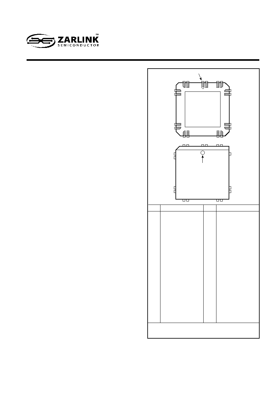
HP44
Figure 1 - Pin connections - top view
Pin
Description
Pin
Description
1
Input bus bit 10
23
Control Direction
2
Input bus bit 9
24
F
pd*
3
Input bus bit 8
25
F
ref*
4
Input bus bit 7
26
+5V
5
Input bus bit 6
27
Ref. osc capacitor
6
Input bus bit 5
28
Ref in/XTAL
7
Input bus bit 4
29
Reference bit 9
8
Input bus bit 3
30
Reference bit 8
9
Input bus bit 2
31
Reference bit 7
10
Input bus bit 1
32
Reference bit 6
11
Input bus bit 0
33
Reference bit 5
12
0V (prescaler)
34
Reference bit 4
13
RF input
35
Reference bit 3
14
RF input
36
Reference bit 2
15
V
CC
+ 5V (prescaler)
37
Reference bit 1
16
V
EE
0V
38
Reference bit 0
17
Lock detect output
39
Phase Detect Enable
18
C-lock detect
40
Phase Detect Gain 1
19
Rset
41
Phase Detect Gain 0
20
Charge pump output
42
Input bus bit 13
21
Charge pump ref.
43
Input bus bit 12
22
F
ref
/F
pd
enable
44
Input bus bit 11
*Fpd and Fref outputs are reversed using the Control Direction
input. The table above is correct when pin 23 is high.
OPTIONAL
PIN 1
REFERENCE
HC44
PIN 1
Features
�
2.8GHz Operating Frequency (IG GRADE)
�
Single 5V Supply Operation
�
High Comparison Frequency 50MHz
�
High Gain Phase Detector 1mA/rad
�
Programmable Phase Detector Gain
�
Zero "Dead Band" Phase Detector
�
Wide range of RF and Reference Divide Ratios
�
Programming by Hard Wired Inputs
�
Low cost plastic package option
�
GPS HI-REL level a screened option
The SP8855E is one of a family of parallel load
synthesisers containing all the elements apart from the loop
amplifier to fabricate a PLL synthesis loop. Other devices in
the series are the SP8852E which is a fully programmable
device requiring two 16 bit words to set the RF and reference
counters, and the SP8854E which has hard wired reference
counter programming and requires a single bit word to pro-
gram the RF divider. The SP8855E replaces the existing
SP8855D.
The SP8855E is intended for applications where a fixed
synthesiser frequency is required although it can also be used
where frequency selection is set by switches. In general the
device will be programmed by connecting the programming
pins to either V
CC
or ground. Additional hard wired inputs can
be used to control the F
pd
and F
ref
outputs set the control
direction of the loop and select the phase detector gain.
Another input may be used to disable the phase detector
output.
The device is available in both plastic (HP) and ceramic
(HC) J-leaded 44-lead chip carrier. Ambient temperature
ranges available are shown in the ordering information.
Absolute Maximum Ratings
Supply voltage
-0.3V to 6V
Storage temperature
-65
�C to +150�C
Operating temperature
-55
�C to +100�C
Prescaler & reference Input Voltage
2.5V p-p
Data Inputs
V
CC
+0.3V
V
EE
-0.3V
Junction temperature
+ 175
�C (HC package)
+ 150
�C (HP package)
2
SP8855E
Advance Information
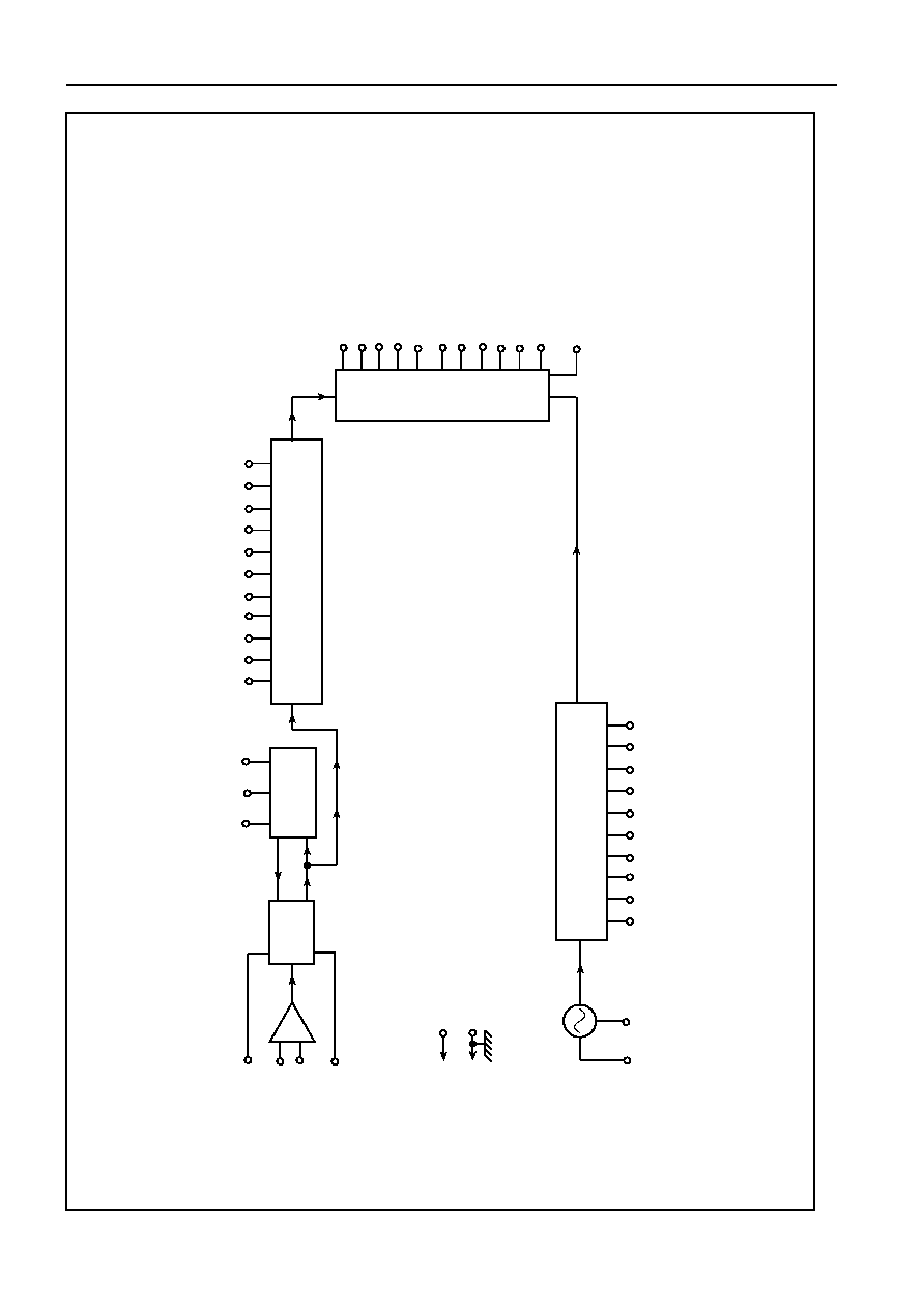
Figure 2 - SP8855E block diagram
0V PRESCALER
Vcc + 5V
PRESCALER
RF INPUT
�
8/9
MODULS
CONTROL
B0
B2
11
10
9
3 BIT
A
COUNTER
11 BIT
M
COUNTER
B3
B13
PHASE
DETECTOR
8
765
4
3
2
1
44
43
42
Fpd
20
V
EE
0V
21
17
19
18
24
25
22
23
40
41
39
CHARGE PUMP OUTPUT
CHARGE PUMP REFERENCE
LOCK DET O/P
R set
C - LOCK DETECT
Fpd *
Fref *
Fpd / Fref ENABLE
CONTROL DIRECTION
PHASE DETECTOR GAIN 1
PHASE DETECTOR GAIN 0
PHASE DETECTOR ENABLE
Fref
10 BIT REFERENCE DIVIDER
38
37
36
35
34
33
32
31
30
29
BIT 9
BIT 0
REFERENCE
DIVIDER
PROGRAMMING
27
28
REFERENCE
CAPACITOR
REFERENCE
CRYSTAL
26
26
+5V
* Fpd and Fref outputs are reversed using the Control
Direction input. Diagram is correct when pin 23 is high.
RF DIVIDER PROGRAMMING

3
SP8855E
Advance Information
PIN Description
PIN
Description
1,2,3,4,5,6,7,8,9,10,11,42,43,44
These pins are the data inputs used to set the RF divider ratio
(M.N+A). Open circuit = 1 (high) on these pins. Inputs are transparent into
the data buffers.
13, 14 (RF INPUT)
Balanced inputs to the RF pre-amplifier. For single ended operation the
signal is AC coupled into pin 13 with pin 14 AC decoupled to ground (or
vice -versa). Pins 13 and 14 are internally DC biased.
17 (LOCK DETECT INPUT)
A current sink into this pin is enabled when the lock detect circuit indicates
lock. Used to give an external indication of phase lock.
18 (C-LOCK DETECT)
A capacitor connected to this point determines the lock detect integrator time
constant and can be used to vary the sensitivity of the phase lock indicator.
19 (Rset)
An external resistor from Pin 19 to V
CC
sets the charge pump output current
20 (CP OUTPUT)
The phase detector output is a single ended charge pump sourcing or
sinking current to the inverting input of an external loop filter.
21 (CP REF)
Connected to the non-inverting input of the loop filter to set the optimum DC
bias.
22 (F
ref
/F
pd
ENABLE
Part of the data input bus. When this pin is logic HI the F
ref
and F
pd
outputs
are enabled. Open circuit = HI
23 (CONTROL DIRECTION)
This pin controls charge pump output direction. For Pin 23 HI the output
sinks current when F
pd
> F
ref
or when the RF phase leads Ref phase. For Pin
23 LO the relationship is reversed. (see table 2).
Changing the state of pin 23 reverses the pins on which Fref and Fpd output
occur. See pin 24 and Pin 25 below for details. Open circuit = HI.
24 = F
pd
if Pin 23 is HI
RF divider output pulses. Fpd = RF input frequency /(M.N+A). Pulse width =
= F
ref
if Pin 23 is LO
8 RF input cycles (1 cycle of the divide by 8 prescaler output).
25 = F
ref
if Pin 223 is HI
Reference divider output pulses. Fref = Reference input frequency/R. Pulse
width = high period of Ref input.
27 (Reference Oscillator Capacitor)
Leave open circuit if an external reference is used. See fig. 5 for typical
connection for use as an onboard crystal oscillator.
28 (Ref IN/XTAL)
This pin is the input buffer amplifier for an external reference signal. This
amplifier provides the active element if an onboard crystal oscillator is used.
29,30,31,32,33,34,35,36,37,38
These pins set the Reference divider ratio R. Open circuit = HI.
39 (Phase Detector ENABLE)
When this pin is HI the phase detector output is enable. Open circuit = HI.
40, 41 (PD Gain)
These pins set the charge pump current multiplication factor (see table 1).
Open circuit = HI.

4
SP8855E
Advance Information
Electrical Characteristics
Guaranteed over the full temperature and supply voltage range (unless otherwise stated)
Temperature T
amb
for KG parts -55
�C and +100�C,
Temperature T
amb
for IG parts -40
�C and +85�, Temperature T
case
for
MA part -55
�C and +125�C Supply Voltage = 4.75V and 5.25V
Characteristics
Pin
Value
Units
Conditions
Min
Typ
Max
Supply current15, 26
180
240
mA
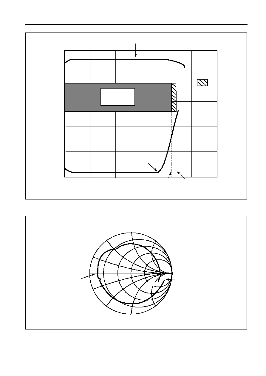
RF input sensitivity
13, 14
-5.0
+7.0
dBm
100MHz to 2.8/2.7GHz See Fig. 3
RF division ratio
13,14,24
56
16383
Reference division ratio
28, 25
1
1023
Comparison frequency
28,24,25
50
MHz
Reference input frequency
28
10
100
MHz
Reference division ratio
2 at frequencies
>50MHz also see Note 1.
Reference input voltage
28
630
1200
2000
mV p-p
Sine Wave 10-100MHz
F
ref
/F
pd
output voltage high
24, 25
- 0.8
Vwrt V
CC
2.2K to 0V
F
red
/F
pd
output voltage low
24, 25
- 1.4
Vwrt V
CC
2.2K to 0V
Lock detect output voltage
17
300
500
mV
I
OUT
= 3mA
Charge pump current at
19,20,21
�1.4
�1.5
�1.7
mA
V
pin
20
= V
pin
21,
multiplication factor = 1
I
pin 19
= 1.6mA
Charge pump current at
19,20,21
�2.0
�2.3
�2.5
mA
V
pin
20
= V
pin
21,
multiplication factor = 1.5
I
pin 19
= 1.6mA
Charge pump current at
19,20,21
�3.4
�3.8
�4.6
mA
V
pin
20
= V
pin
21,
multiplication factor = 2.5
I
pin 19
= 1.6mA
Charge pump current at
19,20,21
�5.4
�6.1
�6.5
mA
V
pin
20
= V
pin
21,
multiplication factor = 4.0
I
pin 19
= 1.6mA
Input bus high logic level
1-11, 22
3.5
V
23, 29-44
Input bus low logic level
1-11, 22
1
V
23,29-44
Input bus current source
1-11,22
-200
�A
V
IN
= 0V
23,29-44
Input bys current sink
1-11, 22
10
�A
V
IN
= V
CC
23,29-44
Up down current matching
20
�5
%
V
pin
20
= V
pin
21,
I
pin 19
= 1.6mA
Charge pump reference
21
V
CC
-0.5
V
I
pin 19
=1.6mA current
voltage
multiplication factor = 1
Charge pump reference
21
V
CC
-1.6
V
I
pin 19
=1.6mA current
voltage
multiplication factor = 4
R
set
current
19
0.5
2
mA
See Note 2
R
set
Voltage 19
1.6
V
I
pin 19
= 1.6mA
Notes: 1. Lower reference frequencies may be used if slew rates are maintained.
2. Pin 19 current x multiplication factor must be less than 5mA if charge pump accuracy is to be maintained.
5
SP8855E
Advance Information
Figure 3 - SP8855E
Figure 4 - R.F. input impedance
TYPICAL OVERLOAD
GUARANTEED
OPERTAING
WINDOW
TYPICAL SENSITIVITY
+20
+10
+7
-5
-10
-20
-30
100MHz
1GHz
10GHz
2.7GHz
2GHz
INPUT DRIVE REQUIREMENTS
2.8GHz
OPERATING
AREA FOR
'IG' PARTS
ONLY
+j2
+j1
+j0.5
+j0.2
0
-j0.2
-j0.5
-j1
-j2
50MHz
2.5GHz
1.1GHz
0.2
0.5
1
Zo = 50