
Obsolescence Notice
This product is obsolete.
This information is available for your
convenience only.
For more information on
Zarlink's obsolete products and
replacement product lists, please visit
http://products.zarlink.com/obsolete_products/

Obsolescence Notice
This product is obsolete.
This information is available for your
convenience only.
For more information on
Zarlink's obsolete products and
replacement product lists, please visit
http://products.zarlink.com/obsolete_products/
VP1058
8-BIT, 25MHz, VIDEO FLASH ADC (SINGLE + 5V SUPPLY)
DS3003 - 3.0
The VP1058 is a low power analog-to-digital flash
converter which requires no preceding sample and hold
stage. Operating from a single +5V supply, it is capable of
digitising analog signals with frequencies up to the Nyquist
limit.
Output data is available in four possible 8-bit formats,
selectable via two digital control inputs, giving either true or
inverted code in binary or offset twos' complement.
FEATURES
s
8-Bit Resolution
s
25MHz Conversion Rate
s
60MHz 3dB Analog Input Bandwidth
s
Single +5V Supply Operation
s
Low Power Consumption (Typically 670mW)
s
+3V to +5V Analog Input Range
s
Selectable Data Format
s
TTL Compatible
s
Direct Replacement for TDC 1058 or CXA 1096P
s
Low Cost
s
No Missing Codes - Guaranteed
APPLICATIONS
s
Digital Television
s
Computing
s
Radar
s
Medical Imaging
s
Nucleonics
s
Low-Cost, High-Speed Data Conversion
OPERATING TEMPERATURE RANGE
Commercial 0
∞
C to 70
∞
C (Still - Air ambient)
ORDERING INFORMATION
VP1058 F CG DPAS (Commercial - Plastic DIL Package, DP28)
VP1058 F CG HPAS (Commercial - Quad Plastic J Lead Package,
HP28)
VP1058 F CG DGAS (Commercial - Ceramic DIL Package, DG28)
ABSOLUTE MAXIMUM RATINGS
Supply voltage
+7V
Analog input, A
IN
V
CC
+0.5
Reference voltage V
RT
, V
RB
V
CC
+0.5
Reference voltage V
RT
, V
RB
2.5V
Digital inputs
V
CC
Mid-ref input current
-50mA to +50mA
Digital output current
-20mA to +20mA
Voltage between AGND and DGND
-0.5V to +0.5V
Voltage between AV
CC
and DV
CC
-0.5V to +0.5V
D
7
MSB
NMINV
D
6
V
RM
D
5
V
RB
D
4
AV
CC
DGND
NC
DV
CC
A
IN
AGND
NC
AGND
A
IN
AGND
NC
DV
CC
AV
CC
DGND
V
RT
NLINV
CONV
D
3
D
0
LSB
D
2
D
1
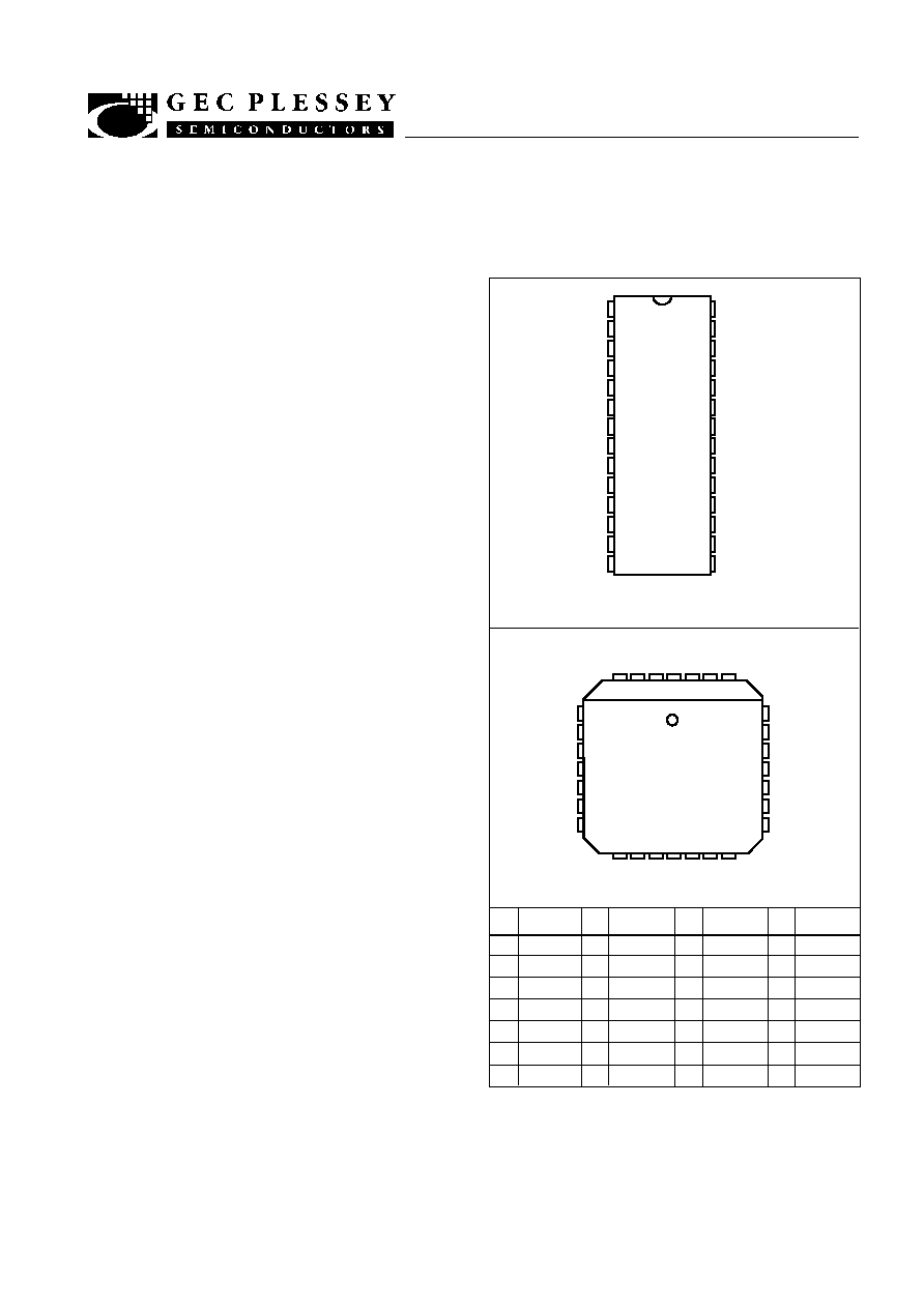
1 28
VP1058
28
27
26
25
24
23
22
21
20
19
18
17
16
15
1
2
3
4
5
6
7
8
9
10
11
12
13
14
Pin
1
2
3
4
5
6
7
Function
D
7
MSB
D
6
D
5
D
4
DGND
DV
CC
AGND
Pin
8
9
10
11
12
13
14
Function
AGND
AGND
DV
CC
DGND
NLINV
D
3
D
2
Function
D
1
D
0
LSB
CONV
V
RT
AV
CC
NC
A
IN
Pin
22
23
24
25
26
27
28
Function
NC
A
IN
NC
AV
CC
V
RB
V
RM
NMINV
Pin
15
16
17
18
19
20
21
Fig.1 Pin Connections (Top View)
HP28
DP28
DG28
ADVANCE INFORMATION
VP1058
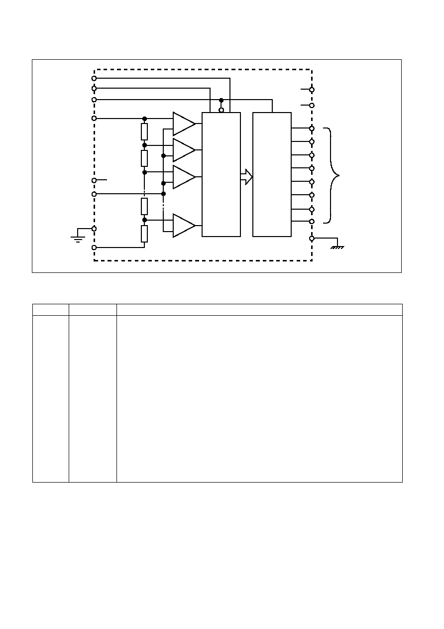
Fig.2 Internal block diagram
16
19.25
6, 10
15
14
13
4
3
2
1
5, 11
27
21, 23
18
17
12
28
7, 8, 9
26
R
R
R
R
AV
CC
DV
CC
D
0
D
7
V
RB
V
RM
V
RT
CONV
NLINV
NMINV
A
IN
R x 256
AGND
DGND
TTL/CMOS
OUTPUTS
MSB
ENCODER
D LATCH
8
Pin No.
1
2 - 4
5, 11
6, 10
7 - 9
12
13 - 15
16
17
18
19, 25
20, 22, 24
21, 23
26
27
28
Description
Most significant bit (output data bit 7)
Output data bits 6 to 4
Digital ground
Digital supply pin (+5V)
Analog ground
Not Least significant bits INvert - inverts data D
0
to D
6
when taken low
Output data bits 3 to 1
Least significant bit (output data bit 0)
Clock input - the rate of input (CONVert) clock signal determines the ADC sampling rate
Top of reference resistor chain
Analog supply pin
Not connected
Analog input pin
Bottom of reference resistor chain
Midpoint of reference resistor - can be used for linearity adjustment
Not Most significant bit INvert - inverts data bit D
7
when taken low
Function
D
7
D
6
- D
4
DGND
DV
CC
AGND
NLINV
D
3
- D
1
D
0
CONV
V
RT
AV
CC
NC
A
IN
V
RB
V
RM
NMINV
PIN DESCRIPTIONS
THERMAL CHARACTERISTICS
Storage Temperature Range
-65
∞
C to +150
∞
C
Maximum Junction Operating Temperature
+175
∞
C
Lead Temperature (soldering 60 seconds)
300
∞
C
DP HP DG
Junction to Ambient
jA
55
57
44
∞
C/W
Junction to Case
jc
14
15
9
∞
C/W
RECOMMENDED OPERATING CONDITIONS
Supply Voltage
5V
±
0.25V
Reference V
RT
5V
±
0.1V
Reference V
RB
3V
±
0.1V
AV
CC
to DV
CC
0V
±
50mV
Analog Input
4V
±
1V

VP1058
V
RT
> V
RB
A
IN
at FS & 1.019MHz
Clock min.high
Clock min.low
Max. conversion rate
Aperture delay
Output data delay
Output hold time
Aperture Jitter
Dynamic Performance
Differential non-linearity
Integral non-linearity
S/N ratio
Effective No. of bits
Characteristic
Symbol
Temp Test level
Min.
Typ.
Max.
Value.
t
PW1
t
PW0
f
MAX
t
AD
t
D
t
HO
DNL
INL
SNR
ENOB
Full
Full
Full
25
25
Full
25
Full
25
25
25
25
Full
25
Full
25
Full
25
4
4
4
5
4
4
4
4
5
1
1
1
4
4
4
4
4
1
4
4
15
15
25
5
5
-0.85
3
50
±
0.5
±
1
45
44.5
44.0
43.5
43.5
43.0
7.2
7.1
7.0
25
30
+1
±
2
ns
ns
MHz
ns
ns
ns
ns
ns
ps
LSB
LSB
dB
dB
dB
dB
dB
dB
bits
bits
bits
A
IN
at FS & 12.5MHz
With standard
LSTLL load
f
CLK
= 25MHz
A
IN
= 1.019MHz
A
IN
= 1.019MHz
A
IN
= 2.438MHz
A
IN
= 2.438MHz
A
IN
= 4.388MHz
A
IN
= 4.388MHz
A
IN
= 1.019MHz
A
IN
= 2.438MHz
A
IN
= 4.388MHz
AC CHARACTERISTICS
Conditions
Units
AV
CC
/DV
CC
I
CC
P
A
IN
I
IN
f
3dB
C
IN
R
D
V
RT
V
RB
V
RTO
V
RBO
R
TC
V
IH
V
IL
I
IH
I
IH
I
IL
V
OH
V
OL
DNL
INL
Power Supply
Supply voltage
Supply current
Power dissipation
Analog Input
Input range
Input bias current
3dB bandwidth
Input capacitance
Reference Ladder
Ladder resistance
Ladder voltage (top)
Ladder voltage (bottom)
Ladder offset (top)
Ladder offset (bottom)
Ladder temp. coeff.
Digital Inputs
Logic '1' voltage
Logic '0' voltage
Logic '1' current
Logic '1' current
Logic '0' current
Digital Outputs
Logic '1' voltage
Logic '0' voltage
Static performance
Differential non-linearity
Integral non-linearity
Full
Full
25
Full
25
Full
Full
25
25
Full
25
Full
Full
25
25
Full
Full
Full
Full
Full
Full
Full
25
Full
25
Full
25
Full
25
4
4
1
4
1
4
4
4
4
4
1
4
4
5
5
5
4
4
4
4
4
4
1
4
1
4
4
4
4
4.75
95
105
500
540
V
RB
60
50
75
2.5
2.0
2.4
2.4
125
125
670
670
150
60
30
90
100
5.0
3.0
15
5
0.33
±
0.5
±
0.5
±
0.5
±
0.5
5.25
165
150
900
830
V
RT
500
145
125
AV
CC
+ 0.1
0.8
350
75
-150
0.4
0.4
V
mA
mA
mW
mW
V
µ
A
MHz
pF
V
V
mV
mV
/
∞
C
V
V
µ
A
µ
A
µ
A
V
V
V
V
LSB
LSB
LSB
LSB
AGND/DGND = 0V
V
I
= V
CC
= MAX
V
I
= 2.4V, V
CC
= MAX
V
I
= 0.4V, V
CC
= MAX
Into a standard
LSTTL load
Characteristic
Symbol
Temp Test level
Min.
Typ.
Max.
Value.
Conditions
Units
ELECTRICAL CHARACTERISTICS
These characteristics are guaranteed over the following conditions conditions (unless otherwise stated):
V
CC
= +5V
±
0.25V, T
amb
= 25
∞
C
DC CHARACTERISTICS