
Obsolescence Notice
This product is obsolete.
This information is available for your
convenience only.
For more information on
Zarlink's obsolete products and
replacement product lists, please visit
http://products.zarlink.com/obsolete_products/

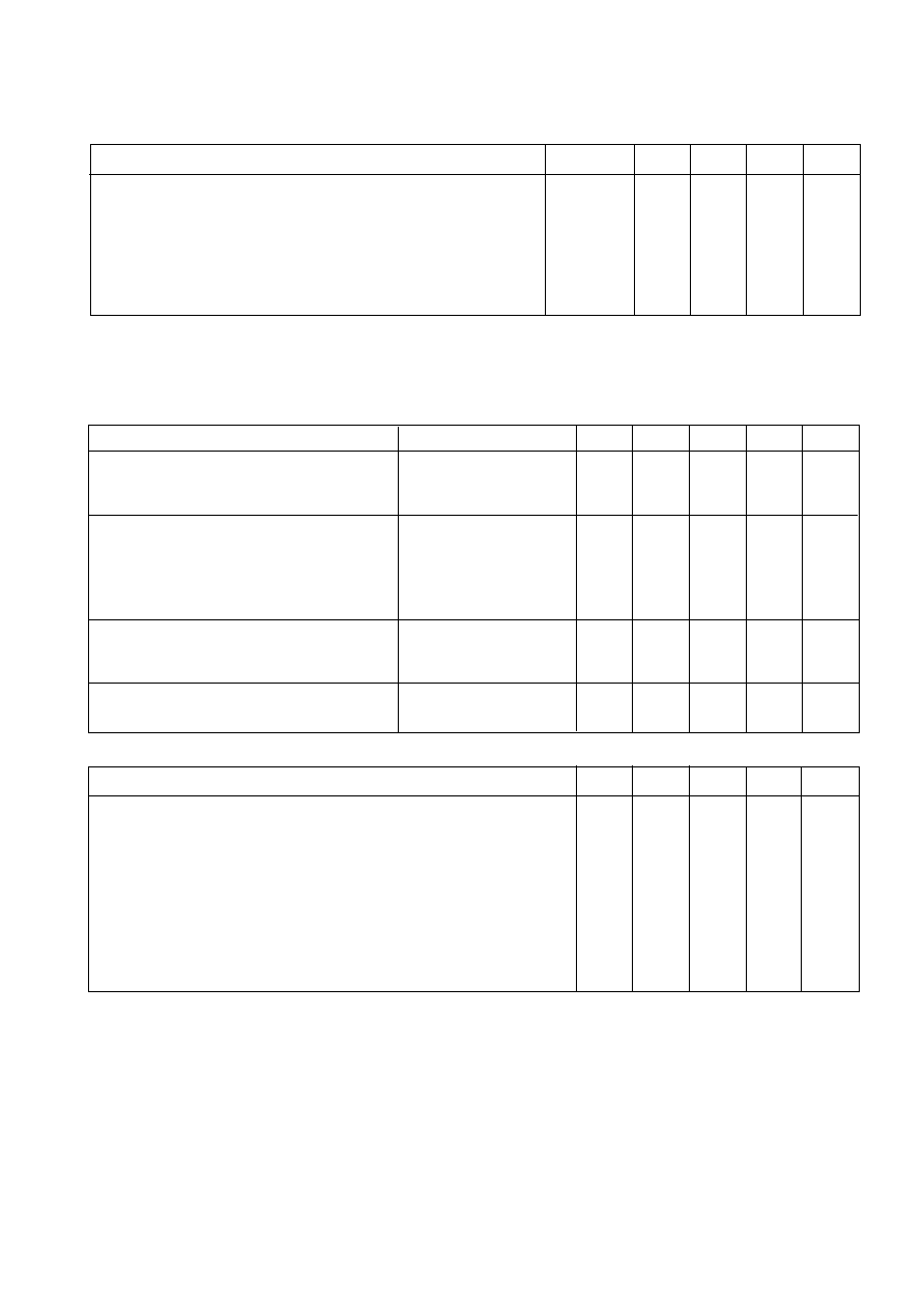
PIN
FUNCTION
PIN
FUNCTION
1
VDD
23
SCL
2
PD5
24
SDA
3
PD6
25
DACCOMP
4
PD7
26
RED/C
5
CLAMP
27
GREEN/Y
6
COMPSYNC
28
AVDD
7
PALID
29
AGND
8
SCSYNC
30
AVDD
9
REFSQ
31
BLUE/CVBS2
10
GND
32
CVBS1
11
VDD
33
VREF
12
FC2
34
RREF
13
FC1
35
AGND
14
FC0
36
AGND
15
HSYNC
37
AVDD
16
VSYNC
38
PD0
17
TTXREQ
39
PD1
18
SA
40
PD2
19
TTXDATA
41
PD3
20
VDD
42
PD4
21
GND
43
GND
22
RESET
44
PXCK
ORDERING INFORMATION
VP5313A/CG/GP1N
VP5513A/CG/GP1N
The VP5313/VP5513 converts digital Y Cr Cb data into
analog PAL or NTSC composite video, and also provides
simultaneous RGB outputs. These additional converters can
optionally provide separate luma and chroma outputs plus a
further composite video channel. All outputs are capable of
driving doubly terminated 75
loads with standard video
levels.
All D/A converters are to 9 bit accuracy, and are provided with
27MHz oversampled data. The latter simplifies the
requirement for external analog anti-aliasing filters, and
reduces the sinx/x distortion inherent in D/A converters.
Separate digital scaling is applied to the chroma data path in
order to make the most efficient use of the 9 bit dynamic range.
The device accepts data inputs complying with CCIR
recommendation 656. In this format 4:2:2 video is multiplexed
onto an 8 bit bus using a 27MHz clock. Active video markers
are embedded into the data stream and extracted by the
VP5313/VP5513. Optionally the user can supply separate
horizontal and vertical syncs, and colour can be genlocked to
an external subcarrier if necessary.
In an alternative operating mode the VP5313/VP5513 can
be configured as the source of sync for the rest of the system.
In this master mode the horizontal and vertical sync pins
become outputs, and any control codes in the CCIR656 bit
stream are ignored.
The VP5313/VP5513 supports the insertion of teletext
data through a serial interface. An internal filter shapes the
data edges.
FEATURES
s
Converts Y, Cr, Cb data to analog RGB and composite
or S-video and composite video
s
Supports CCIR recommendations 601 and 656
s
All digital video encoding
s
Selectable master/slave mode for sync signals
s
Switchable chrominance bandwidth
s
CCIR 624 PAL SMPTE or 170M NTSC compatible
outputs
s
GENLOCK mode
s
I
2
C bus serial microprocessor interface
s
Only VP5313 supports Macrovision anti-taping
Rev. 7.01
s
Line 21 Closed Caption encoding
s
Teletext insertion, fully line programmable
APPLICATIONS
s
Digital Cable TV
s
Digital Satellite TV
s
Multi-media
s
Video games
s
Digital VCRs
s
Karaoke
Fig.1 Pin connections (top view)
GP44
1
11
33
23
12
22
44
34
VP5313/VP5513
NTSC/PAL Digital Video Encoder
Supersedes DS4509 1.9 September 1997 edition
DS4509 - 2.2 October 1998
VP5313/VP5513
2
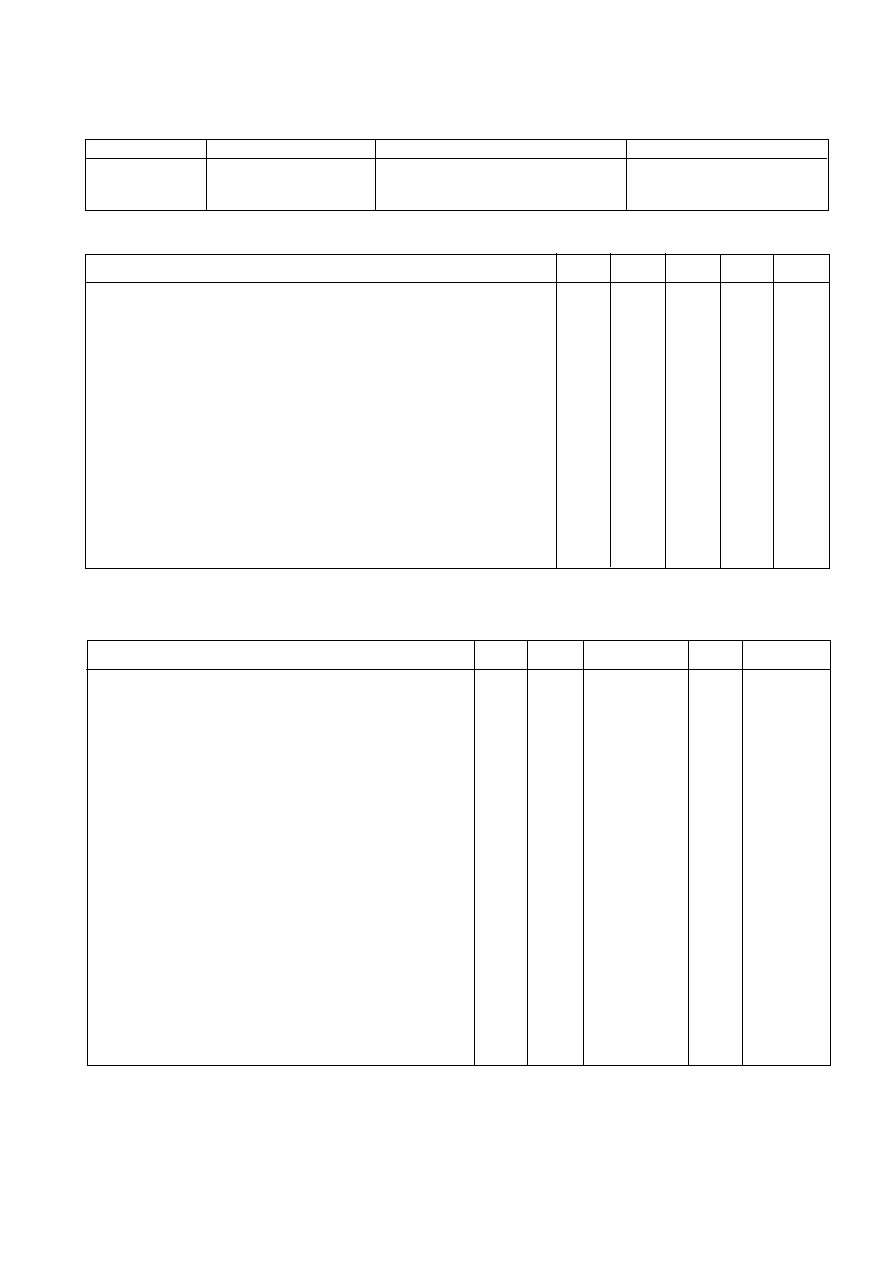
RECOMMENDED OPERATING CONDITIONS
Parameter
Min.
Typ.
Max.
Units
Power supply voltage
Power supply current (including analog outputs)
1
Power supply current (including analog outputs)
2
Input clock frequency
SCL clock frequency
Analog video output load
DAC gain resistor
Ambient operating temperature
Symbol
VDD, AVDD
IDD
IDD
PXCK
f
SCL
4.75
-50ppm
0
5.25
230
190
+50ppm
500
70
V
mA
mA
MHz
kHz
∞
C
5.00
27.00
37.5
730
1.
All four DACs driving 37R5 loads
2.
All four DACs driving 75R loads
ELECTRICAL CHARACTERISTICS
Test conditions (unless otherwise stated): As specified in Recommended Operating Conditions
DC CHARACTERISTICS
VIN
VIL
VIH
VIL
IIH
IIL
VOH
VOL
VOL
2.0
0.7VDD
3.7
0.8
0.3VDD
10
-10
0.4
0.6
V
V
V
V
µ
A
µ
A
V
V
V
Parameter
Conditions
VIN = VDD
VIN = VSS
IOH = -1mA
IOL = +4mA
IOL = +6mA
Symbol
Min.
Typ.
Max.
Units
Digital Inputs TTL compatible (except SDA, SCL)
Input high voltage
Input low voltage
Digital Inputs SDA, SCL
Input high voltage
Input low voltage
Input high current
Input low current
Digital Outputs CMOS compatible
Output high voltage
Output low voltage
Digital Output SDA
Output low voltage
66.83
1.00
8k
1.3899
34.15
50
DC CHARACTERISTICS DACs
INL
DNL
V
REF
Z
R
I
REF
0.95
±
1.5
±
1
±
5
1.05
LSB
LSB
%
µ
A
V
mA
mA
pV-s
Parameter
Symbol
Min.
Typ.
Max.
Units
Accuracy (each DAC)
Integral linearity error
Diffential linearity error
DAC matching error
Monotonicity
LSB size
Internal reference voltage
Internal reference voltage output impedance
Reference Current (V
REF
/R
REF
) R
REF
= 730
Maximum output
Peak Glitch Energy (see fig.3)
guaranteed
ABSOLUTE MAXIMUM RATINGS
Supply voltage
VDD, AVDD
-0∑3 to 7∑0V
Voltage on any non power pin
-0∑3 to VDD+0∑3V
Ambient operating temperature
0 to 70
∞
C
Storage temperature
-55
∞
C to 150
∞
C
Note: Stresses exceeding these listed under Absolute
Maximum Ratings may induce failure. Exposure to Absolute
Maximum Ratings for extended periods may reduce
reliability. Functionality at or above these conditions is not
implied.
VP5313/VP5513
3
Pins
All pins
All pins
Notes
Meets Mil-Std-883 Class 2
Test Levels
2kV on 100pF through 1k5
200V on 200pF through 0
& 500nH
Test
Human body model
Machine model
Luminance bandwidth
Chrominance bandwidth (Extended B/w mode)
Chrominance bandwidth (Reduced B/w mode)
Burst frequency (NTSC)
Burst frequency (PAL-B, D,G,H,I)
Burst frequency (PAL-N Argentina)
Burst cycles (NTSC and PAL-N)
Burst cycles ( PAL-B, D, G, H,I)
Burst envelope rise / fall time (NTSC )
Burst envelope rise / fall time (PAL-B, D, G, H, I, N)
Analog video sync rise / fall time (NTSC)
Analog video sync rise / fall time (PAL-B, D, G, H,I)
Analog video blank rise / fall time (NTSC )
Analog video blank rise / fall time (PAL-B, D, G, H,I)
Differential gain
Differential phase
Signal to noise ratio (unmodulated ramp)
Chroma AM signal to noise ratio (100% red field)
Chroma PM signal to noise ratio (100% red field)
Hue accuracy
Colour saturation accuracy
Residual sub carrier
Luminance / chrominance delay
VIDEO CHARACTERISTICS (NTSC, PAL COMPOSITE VIDEO)
Parameter
1
1
-61
-56
-58
2.5
2.5
10
Max.
Symbol
Min.
Typ.
5.5
1.3
650
3.57954545
4.43361875
3.58205625
9
10
300
300
145
245
145
245
-60
5
MHz
MHz
kHz
MHz
MHz
MHz
Fsc cycles
Fsc cycles
ns
ns
ns
ns
ns
ns
% pk-pk
∞
pk-pk
dB
dB
dB
%
%
dB
ns
Units
ESD COMPLIANCE
19.98
1.337
33.75
17.63
1.40
7.61
7.61
0.40
18.70
8.01
8.01
0.00
DC CHARACTERISTICS DACs
mA
mA
mA
mA
mA
mA
mA
mA
mA
mA
mA
mA
Parameter
Symbol
Min.
Typ.
Max.
Units
RGB outputs:
Peak level
Black level
CVBS1, 2 Y and C outputs - NTSC (pedestal enabled)
Maximum output, relative to sync bottom
White level relative to black level
Black level relative to blank level
Blank level relative to sync level
Colour burst peak - peak
DC offset (bottom of sync)
CVBS1, 2, Y and C outputs - PAL
White level relative to black level
Black level relative to sync level
Colour burst peak - peak
DC offset (bottom of sync)
All figures are for: RREF = 730
; if RL = 75
then RREF = 1460

VP5313/VP5513
4
Pin Name
Pin No.
Description
PD0-7
2-4,
8 Bit Pixel Data inputs clocked by PXCK. PD0 is the least significant bit. These pins are
internally pulled low.
PXCK
44
27MHz Pixel Clock input. The VP5313/VP5513 internally divides PXCK by two to provide the
pixel clock.
SA
18
Slave address select.
SCL
23
Standard I
2
C bus serial clock input.
SDA
24
Standard I
2
C bus serial data input/output.
FC0-2
12-14
Field Counter output in master sync mode.
REFSQ
9
Reference square wave input used only during Genlock mode.
SCSYNC
8
Subcarrier sync input, (synchronises phase quadrant in 4xfsc genlock mode), see fig 6.
PALID
7
PAL IDENT input, controls swinging colour burst phase in PAL genlock mode.
COMPSYNC
6
Composite sync pulse output. This is an active low output signal.
CLAMP
5
The CLAMP output signal is synchronised to COMPSYNC output and indicates the position of
the BURST pulse, (lines 10-263 and 273-525 for NTSC; lines 6-310 and 319-623 for PAL-
B,D,G,I,N(Argentina)).
TTXREQ
17
Teletext Data Request output, requests next line of teletext data.
TTXDATA
19
Teletext Data input.
HSYNC
15
Horizontal Sync, output in master mode, input in slave mode
VSYNC
16
Vertical Sync, output in master mode, input in slave mode
RESET
22
Master reset. This is an asynchronous, active low, input signal and must be asserted for a
minimum 200ns in order to reset the VP5313/VP5513.
VREF
33
Voltage reference output. This output is nominally 1∑0V and should be decoupled with a
100nF capacitor to GND.
RREF
34
DAC full scale current control. A resistor connected between this pin and GND sets the
magnitude of the video output current. An internal loop amplifier controls a reference current
flowing through this resistor so that the voltage across it is equal to the Vref voltage. This
reference current has a weighting equal to 20.8 LSB's.
DACCOMP
25
DAC compensation. A 100nF ceramic capacitor must be connected to AVDD.
CVBS1
32
Composite video output. These are high impedance current source outputs. A DC path to
GND must exist from each of these pins.
BLUE/CVBS2
31
Blue or composite DAC output. Output type as CVBS1.
GREEN/Y
27
Green or luminance DAC output. Output type as CVBS1.
RED/C
26
Red or chrominance DAC output. Output type as CVBS1.
VDD
1, 11, 20
Positive supply input. All VDD pins must be connected.
AVDD
37,28,30
Analog positive supply input. All AVDD pins must be connected.
GND
10,21,43
Negative supply input. All GND pins must be connected.
AGND
36,29,35
Analog negative supply input. All AGND pins must be connected.
PIN DESCRIPTIONS
38-42