 | –≠–ª–µ–∫—Ç—Ä–æ–Ω–Ω—ã–π –∫–æ–º–ø–æ–Ω–µ–Ω—Ç: WL600C | –°–∫–∞—á–∞—Ç—å:  PDF PDF  ZIP ZIP |

Obsolescence Notice
This product is obsolete.
This information is available for your
convenience only.
For more information on
Zarlink's obsolete products and
replacement product lists, please visit
http://products.zarlink.com/obsolete_products/

WL600C
2.4 - 2.5GHz RF and IF Circuit
Preliminary Information
DS4581
ISSUE 2.1
August 1997
Ordering Information
WL600C/KG/GP1R
Figure 1 - Pin connections - top view
Features
∑
Part of DE6038 chipset (WL800, WL102)
∑
High level of integration
∑
Low noise figure
∑
Low power consumption
∑
High data rates with comparator for 2 level FSK
∑
Minimal external components
∑
48 lead LQFP package
Absolute Maximum Ratings
Supply voltage Vcc
4V
Transmit/Receive and standby input
-0.5 to Vcc +0.5V
Current consumption
TBD
Junction temperature Tj
150
∞
ESD protection
2KV
Related Documents
Datasheets WL800/102 DE6038
The WL600C is a 2.4-2.5GHz RF transmitter and
receiver chip for use in digital radio, and operates from a
supply voltage of 2.7 - 3.6V. It is designed to work with the
Zarlink Semiconductor WL800 frequency synthesiser and
the WL102 WLAN controller chip which together make up
the DE6038 frequency hopping Wireless Local Area
Network (WLAN) transceiver.
The receiver circuit contains a low noise amplifier,
image rejecting mixer, IF limiting strip with RSSI and a
quadrature demodulator. There is also a power amplifier
driver stage and ramp control facility for use in transmit.
LQFP48
PIN 48
PIN 1 IDENT
PIN 1
Pin
Description
Pin
Description
1
QUAD+
25
VCC_RF
2
QUAD-
26
GND_RF
3
GND_IF
27
VCC_LNA
4
DEMOD_OUT+
28
GND_RF
5
DEMOD_OUT-
29
RF_IN
6
RSSI
30
LNA_DEGEN
7
CLAMP_SET
31
LNA_DEGEN
8
CCA_THRESHOLD
32
DRIVE
9
VCC_IFSTRIP
33
VCC_PA
10
DECOUPLE_LOG-
34
GND_RF
11
DECOUPLE_LOG+
35
RAMP_CAP
12
IF_IN+
36
PA_ON
13
IF_IN-
37
STDBYB
14
CCAB
38
TX/RXB
15
GND_IF
39
GND_LO
16
BUFFER_IN+
40
LO_IN
17
BUFFER_IN-
41
VCC_LO
18
VCC_DATA
42
DATA_IN+
19
RXD
43
DATA_IN-
20
RXDB
44
BUFFER_OUT-
21
GND_RF
45
BUFFER_OUT+
22
IF_OUT-
46
CLAMP-
23
IF_OUT+
47
CLAMP+
24
GND_PADDLE
48
GND_PADDLE
2
WL600C
Preliminary Information
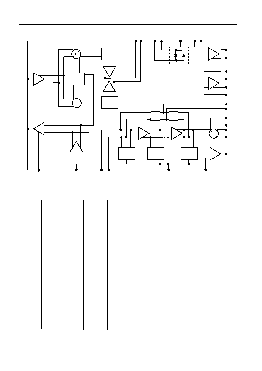
Figure 2 - WL600C block diagram
ACTIVE
CLAMP
CIRCUIT
IMAGE
REJECT
MIXER
PHASE
SHIFT
PHASE
SHIFT
29
LNA
IMAGE
REJECT
MIXER
32
PA DRIVE
BUFFER
LO
BUFFER
35
40
12
13
6
8
PHASE
SHIFT
22
23 46
47
7
42
43
DATA
SLICE
19
20
16
44
45
X2
BUFFER
AMP
17
10
11
1
2
4
5
14
COMPARATOR
DETECTORS
IF STRIP
DEVICE PIN OUT
Pin
Ref
Type
Description
1
QUAD+
I/O
Quadrature demodulator tank circuit connection
2
QUAD -
I/O
Quadrature demodulator tank circuit connection
3
GND_IF
GND
Ground for IF strip circuitry
4
DEMOD_OUT +
OUT
Demodulator output
5
DEMOD_OUT -
OUT
Demodulator output
6
RSSI
OUT
RSSI detector analogue output
7
CLAMP_SET
IN
Sets clamp knee voltage
8
CCA_THRESHOLD
IN
Sets level at which CCA comparator will switch
9
VCC_IFSTRIP
VCC
Power supply for log amp, demod, and internal references
10
DECOUPLE_LOG -
I/O
Decoupling for log amp feedback network, AC couple
11
DECOUPLE_LOG +
I/O
Decoupling for log amp feedback network, AC couple
12
IF_IN +
IN
Log amp input, AC couple
13
IF_IN -
IN
Log amp input, AC couple
14
CCAB
OUT
CCA comparator output: signal = logic high, clear = logic low
15
GND_IF
GND
Ground for IF strip circuitry
16
BUFFER_IN +
IN
x 2 buffer input
17
BUFFER_IN -
IN
x 2 buffer input
18
VCC_DATA
VCC
Power supply for clamp, data comparator and buffer amp
19
RXD
OUT
Data comparator output

3
WL600C
Preliminary Information
Pin
Ref
Type
Description
20
RXDB
OUT
Data comparator output
21
GND_RF
GND
Ground for LNA, mixer, IF summation, and PA driver circuits
22
IF_OUT-
OUT
Downconverter output, requires external load and RFC
23
IF_OUT+
OUT
Downconverter output, requires external load and RFC
24
GND_PADDLE
GND
Ground for substrate and package paddle
25
VCC_RF
VCC
Power supply for mixer, summation, and PA ramp circuits
26
GND_RF
GND
Ground for LNA, mixer, IF summation, and PA driver circuits
27
VCC_LNA
VCC
Power supply for LNA
28
GND_RF
GND
Ground for LNA, mixer, IF summation, and PA driver circuits
29
RF_IN
IN
LNA input, AC couple
30
LNA_DEGEN
I/O
LNA degeneration, connect to ground
31
LNA_DEGEN
I/O
LNA degeneration, connect to ground
32
DRIVE
OUT
Power amplifier driver output, requires external load and RFC
33
VCC_PA
VCC
Power supply for power amplifier driver
34
GND_RF
GND
Ground for LNA, mixer, IF summation, and PA driver circuits
35
RAMP_CAP
I/O
PA ramp circuit timing capacitor connection
36
PA_ON
IN
PA ramp circuit control input:
PA on = logic high, PA off = logic low
37
STDBYB
IN
Power down control input:
active= logic high, standby = logic low
38
TX/RXB
IN
Transmit/Receive control input:
transmit = logic high, receive = logic low
39
GND_LO
GND
Ground for LO buffer, phaseshifter, and standby circuitry
40
LO_IN
IN
Local oscillator input, AC couple
41
VCC_LO
VCC
Power supply for LO buffer, phaseshifter, and standby circuitry
42
DATA_IN+
IN
Data comparator input
43
DATA_IN-
IN
Data comparator input
44
BUFFER_OUT-
OUT
x2 buffer output
45
BUFFER_OUT+
OUT
x2 buffer output
46
CLAMP -
I/O
Data clamp, knee voltage set by pin 7, AC couple
47
CLAMP +
I/O
Data clamp, knee voltage set by pin 7, AC couple
48
GND_PADDLE
GND
Ground for substrate and package paddle

4
WL600C
Preliminary Information
Characteristic
Value
Unit
Condition
Min
Typ
Max
Supply current (transmit)
50
mA
Supply current (Receive)
60
mA
Supply current in standby
0.3
mA
PA DRIVER & RAMP CIRCUIT
Logic low voltage
0
0.8
V
Ramp down
Logic high voltage
Vcc-0.7
Vcc
V
Ramp up
Logic Input current
10
µ
A
Ramp capacitor charge Current
250
µ
A
Ramp capacitor voltage swing
1
V
Output power
-2
2
dBm
Output band
2.4
2.5
GHz
Max to Min power out ratio
20
dB
RECEIVER LOW NOISE
AMPLIFIER & MIXERS
Conversion gain
19
22
dB
Differential into 600Ohms
3rd order intercept point
-10
dBm
1dB input gain compression
-22
dBm
Noise figure
7
10
dB
Matched to 50Ohms
Input impedance
2.4GHz
13+j20
Ohms
2.45GHz
15+j30
2.5GHz
20+j50
Image frequency rejection
25
dB
Local oscillator input level
-16
dBm
Local oscillator input impedance
15-j40
Ohms
IF output impedance
600
Ohms
With external 900
resistor
TRANSMIT/RECEIVE INPUT
Logic low voltage
0
0.8
V
Receive mode
Logic high voltage
Vcc-0.7
Vcc
V
Transmit mode
Input current
10
µ
A
Electrical Characteristics
These characteristics are guaranteed over the following conditions (unless otherwise stated):
T
AMB
= -20
∞
C to + 85
∞
C V
CC
= 2.7V to 3.6V,