
1
Zarlink Semiconductor Inc.
Zarlink, ZL and the Zarlink Semiconductor logo are trademarks of Zarlink Semiconductor Inc.
Copyright 2004, Zarlink Semiconductor Inc. All Rights Reserved.
Features
� QPSK tuner for quadrature down conversion from
L-band to Zero IF
� Compatible with DSS and DVB formats (QPSK)
� Symbol rate range 1 to 45 MSps
� Power & forget, fully integrated, alignment free,
local oscillator
� Integrated baseband filters with bandwidth adjust
from 4 to 40 MHz
� Good immunity to strong adjacent undesired
channels
� Selectable RF bypass
� I�C bus interface with 3V3 compatible logic levels
� Integrated RF loop through for cascaded tuner
applications
� Power saving mode/hardware power down
� Optimized front end solution when partnered with
Zarlink ZL10312 demodulator
Applications
� Satellite receiver systems
Description
The ZL10036 is a single chip wideband direct
conversion tuner, with integral RF bypass, optimized
for application in digital satellite receiver systems.
The device offers a highly integrated solution to a
satellite tuner function, incorporating an I�C bus
interface controller, a low phase noise PLL frequency
synthesizer, a quadrature phase split tuner, a fully
integrated local oscillator which requires no production
set up, and adjustable baseband channel filters.
The I�C bus interface controls all of the tuner
functionality including the PLL frequency synthesizer,
the bypass disable and the baseband gain and
bandwidth adjust.
July 2004
Ordering Information
ZL10036LDG
40-pin QFN
(trays)
ZL10036LDF
40-pin QFN
(tape and reel)
ZL10036LDG1 40-pin QFN*
(trays)
ZL10036LDF1 40-pin QFN*
(tape and reel)
*Pb free
-10
�C to +85�C
ZL10036
Digital Satellite Tuner with RF Bypass
Data Sheet
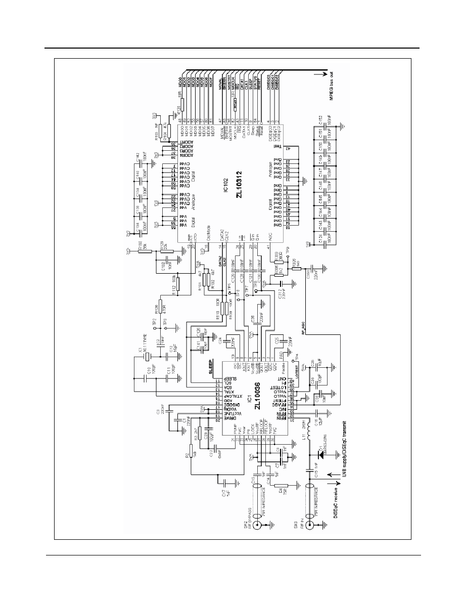
Figure 1 - Basic Block Diagram
ZL10036
Data Sheet
2
Zarlink Semiconductor Inc.
Figure 2 - Typical Application Circuit ZLE10532 (SNIM-9r2) using ZL10312 Demodulator

ZL10036
Data Sheet
Table of Contents
3
Zarlink Semiconductor Inc.
1.0 Overview . . . . . . . . . . . . . . . . . . . . . . . . . . . . . . . . . . . . . . . . . . . . . . . . . . . . . . . . . . . . . . . . . . . . . . . . . . . . . 11
1.1 Conventions in this Manual . . . . . . . . . . . . . . . . . . . . . . . . . . . . . . . . . . . . . . . . . . . . . . . . . . . . . . . . . . . . 11
2.0 Functional Description . . . . . . . . . . . . . . . . . . . . . . . . . . . . . . . . . . . . . . . . . . . . . . . . . . . . . . . . . . . . . . . . . 12
2.1 Quadrature Down-Converter . . . . . . . . . . . . . . . . . . . . . . . . . . . . . . . . . . . . . . . . . . . . . . . . . . . . . . . . . . . 12
2.2 AGC Functions . . . . . . . . . . . . . . . . . . . . . . . . . . . . . . . . . . . . . . . . . . . . . . . . . . . . . . . . . . . . . . . . . . . . . 12
2.2.1 RF . . . . . . . . . . . . . . . . . . . . . . . . . . . . . . . . . . . . . . . . . . . . . . . . . . . . . . . . . . . . . . . . . . . . . . . . . . 13
2.2.2 Baseband . . . . . . . . . . . . . . . . . . . . . . . . . . . . . . . . . . . . . . . . . . . . . . . . . . . . . . . . . . . . . . . . . . . . . 15
2.3 RF bypass . . . . . . . . . . . . . . . . . . . . . . . . . . . . . . . . . . . . . . . . . . . . . . . . . . . . . . . . . . . . . . . . . . . . . . . . . 16
2.4 Baseband Filter . . . . . . . . . . . . . . . . . . . . . . . . . . . . . . . . . . . . . . . . . . . . . . . . . . . . . . . . . . . . . . . . . . . . . 17
2.5 Local Oscillator . . . . . . . . . . . . . . . . . . . . . . . . . . . . . . . . . . . . . . . . . . . . . . . . . . . . . . . . . . . . . . . . . . . . . 18
2.6 PLL Frequency Synthesizer . . . . . . . . . . . . . . . . . . . . . . . . . . . . . . . . . . . . . . . . . . . . . . . . . . . . . . . . . . . 18
2.7 Control Logic . . . . . . . . . . . . . . . . . . . . . . . . . . . . . . . . . . . . . . . . . . . . . . . . . . . . . . . . . . . . . . . . . . . . . . . 19
3.0 User Control . . . . . . . . . . . . . . . . . . . . . . . . . . . . . . . . . . . . . . . . . . . . . . . . . . . . . . . . . . . . . . . . . . . . . . . . . . 19
3.1 I/O Pins . . . . . . . . . . . . . . . . . . . . . . . . . . . . . . . . . . . . . . . . . . . . . . . . . . . . . . . . . . . . . . . . . . . . . . . . . . . 19
3.1.1 LOCK - Pin 25 . . . . . . . . . . . . . . . . . . . . . . . . . . . . . . . . . . . . . . . . . . . . . . . . . . . . . . . . . . . . . . . . . 19
3.1.2 SLEEP - Pin 11 . . . . . . . . . . . . . . . . . . . . . . . . . . . . . . . . . . . . . . . . . . . . . . . . . . . . . . . . . . . . . . . . 19
3.1.3 Output Ports, P1 & P0 - Pins 39 & 24 . . . . . . . . . . . . . . . . . . . . . . . . . . . . . . . . . . . . . . . . . . . . . . . 19
3.2 Device Address Selection . . . . . . . . . . . . . . . . . . . . . . . . . . . . . . . . . . . . . . . . . . . . . . . . . . . . . . . . . . . . . 20
3.3 Read Register . . . . . . . . . . . . . . . . . . . . . . . . . . . . . . . . . . . . . . . . . . . . . . . . . . . . . . . . . . . . . . . . . . . . . . 20
3.3.1 Power-On Reset Indicator (POR bit) . . . . . . . . . . . . . . . . . . . . . . . . . . . . . . . . . . . . . . . . . . . . . . . . 20
3.3.2 Frequency & Phase Lock (FL bit). . . . . . . . . . . . . . . . . . . . . . . . . . . . . . . . . . . . . . . . . . . . . . . . . . . 20
3.3.3 Internal Operation Indicators (X Bits) . . . . . . . . . . . . . . . . . . . . . . . . . . . . . . . . . . . . . . . . . . . . . . . . 21
3.4 Write Registers . . . . . . . . . . . . . . . . . . . . . . . . . . . . . . . . . . . . . . . . . . . . . . . . . . . . . . . . . . . . . . . . . . . . . 21
3.4.1 Register Sub-Addressing . . . . . . . . . . . . . . . . . . . . . . . . . . . . . . . . . . . . . . . . . . . . . . . . . . . . . . . . . 21
3.4.2 Register Mapping . . . . . . . . . . . . . . . . . . . . . . . . . . . . . . . . . . . . . . . . . . . . . . . . . . . . . . . . . . . . . . . 22
3.4.3 Synthesizer Division Ratio (2
14
:2
0
Bits) . . . . . . . . . . . . . . . . . . . . . . . . . . . . . . . . . . . . . . . . . . . . . . 23
3.4.4 RF Gain (RFG Bit) . . . . . . . . . . . . . . . . . . . . . . . . . . . . . . . . . . . . . . . . . . . . . . . . . . . . . . . . . . . . . . 23
3.4.5 Baseband Pre-Filter Gain Adjust (BA1:0 Bits) . . . . . . . . . . . . . . . . . . . . . . . . . . . . . . . . . . . . . . . . . 23
3.4.6 Baseband Post-Filter Gain (BG1:0 Bits) . . . . . . . . . . . . . . . . . . . . . . . . . . . . . . . . . . . . . . . . . . . . . 23
3.4.7 RF Bypass Disable (LEN Bit) . . . . . . . . . . . . . . . . . . . . . . . . . . . . . . . . . . . . . . . . . . . . . . . . . . . . . . 24
3.4.8 Output Port Controls (P1 & P0 Bits). . . . . . . . . . . . . . . . . . . . . . . . . . . . . . . . . . . . . . . . . . . . . . . . . 24
3.4.9 Power Down (PD Bit) . . . . . . . . . . . . . . . . . . . . . . . . . . . . . . . . . . . . . . . . . . . . . . . . . . . . . . . . . . . . 24
3.4.10 Logic Reset (CLR Bit) . . . . . . . . . . . . . . . . . . . . . . . . . . . . . . . . . . . . . . . . . . . . . . . . . . . . . . . . . . 24
3.4.11 Charge Pump Current (C1 & C0 Bits) . . . . . . . . . . . . . . . . . . . . . . . . . . . . . . . . . . . . . . . . . . . . . . 24
3.4.12 Reference Division Ratios (R4:0 Bits) . . . . . . . . . . . . . . . . . . . . . . . . . . . . . . . . . . . . . . . . . . . . . . 25
3.4.13 Baseband Filter Resistor Switching (RSD) . . . . . . . . . . . . . . . . . . . . . . . . . . . . . . . . . . . . . . . . . . 25
3.4.14 Baseband Filter Bandwidth (BF6:1 & BR4:0 Bits) . . . . . . . . . . . . . . . . . . . . . . . . . . . . . . . . . . . . . 25
3.4.15 LO Test (TL Bit) . . . . . . . . . . . . . . . . . . . . . . . . . . . . . . . . . . . . . . . . . . . . . . . . . . . . . . . . . . . . . . . 25
4.0 Software . . . . . . . . . . . . . . . . . . . . . . . . . . . . . . . . . . . . . . . . . . . . . . . . . . . . . . . . . . . . . . . . . . . . . . . . . . . . . 26
4.1 Power-on Software Initialization . . . . . . . . . . . . . . . . . . . . . . . . . . . . . . . . . . . . . . . . . . . . . . . . . . . . . . . . 26
4.2 Changing Channel. . . . . . . . . . . . . . . . . . . . . . . . . . . . . . . . . . . . . . . . . . . . . . . . . . . . . . . . . . . . . . . . . . . 26
4.3 Symbol Rate and Filter Calculations . . . . . . . . . . . . . . . . . . . . . . . . . . . . . . . . . . . . . . . . . . . . . . . . . . . . . 26
4.3.1 Determining the Filter Bandwidth from the Symbol Rate . . . . . . . . . . . . . . . . . . . . . . . . . . . . . . . . . 26
4.3.2 Calculating the Filter Bandwidth. . . . . . . . . . . . . . . . . . . . . . . . . . . . . . . . . . . . . . . . . . . . . . . . . . . . 27
4.3.3 Determining the Values of BF and BR . . . . . . . . . . . . . . . . . . . . . . . . . . . . . . . . . . . . . . . . . . . . . . . 27
4.3.3.1 Calculating the Value of BR . . . . . . . . . . . . . . . . . . . . . . . . . . . . . . . . . . . . . . . . . . . . . . . . . . 27
4.3.3.2 Calculating the Value of BF . . . . . . . . . . . . . . . . . . . . . . . . . . . . . . . . . . . . . . . . . . . . . . . . . . 27
4.3.4 Filter Bandwidth Programming Examples . . . . . . . . . . . . . . . . . . . . . . . . . . . . . . . . . . . . . . . . . . . . 28
4.4 Programming Sequence for Filter Bandwidth Changes . . . . . . . . . . . . . . . . . . . . . . . . . . . . . . . . . . . . . . 28
5.0 Application Notes . . . . . . . . . . . . . . . . . . . . . . . . . . . . . . . . . . . . . . . . . . . . . . . . . . . . . . . . . . . . . . . . . . . . . 29
5.1 Thermal Considerations . . . . . . . . . . . . . . . . . . . . . . . . . . . . . . . . . . . . . . . . . . . . . . . . . . . . . . . . . . . . . . 29
5.2 Crystal Oscillator Notes . . . . . . . . . . . . . . . . . . . . . . . . . . . . . . . . . . . . . . . . . . . . . . . . . . . . . . . . . . . . . . . 30

ZL10036
Data Sheet
Table of Contents
4
Zarlink Semiconductor Inc.
6.0 Electrical characteristics. . . . . . . . . . . . . . . . . . . . . . . . . . . . . . . . . . . . . . . . . . . . . . . . . . . . . . . . . . . . . . . . 31
6.1 Test Conditions . . . . . . . . . . . . . . . . . . . . . . . . . . . . . . . . . . . . . . . . . . . . . . . . . . . . . . . . . . . . . . . . . . . . . 31
6.2 Absolute Maximum Ratings. . . . . . . . . . . . . . . . . . . . . . . . . . . . . . . . . . . . . . . . . . . . . . . . . . . . . . . . . . . . 31
6.3 Recommended Operating Conditions . . . . . . . . . . . . . . . . . . . . . . . . . . . . . . . . . . . . . . . . . . . . . . . . . . . . 32
6.4 DC Characteristics. . . . . . . . . . . . . . . . . . . . . . . . . . . . . . . . . . . . . . . . . . . . . . . . . . . . . . . . . . . . . . . . . . . 32
6.5 AC Characteristics. . . . . . . . . . . . . . . . . . . . . . . . . . . . . . . . . . . . . . . . . . . . . . . . . . . . . . . . . . . . . . . . . . . 33

ZL10036
Data Sheet
List of Figures
5
Zarlink Semiconductor Inc.
Figure 1 - Basic Block Diagram . . . . . . . . . . . . . . . . . . . . . . . . . . . . . . . . . . . . . . . . . . . . . . . . . . . . . . . . . . . . . . . . 1
Figure 2 - Typical Application Circuit ZLE10532 (SNIM-9r2) using ZL10312 Demodulator . . . . . . . . . . . . . . . . . . . 2
Figure 3 - Functional Block Diagram . . . . . . . . . . . . . . . . . . . . . . . . . . . . . . . . . . . . . . . . . . . . . . . . . . . . . . . . . . . 12
Figure 4 - AGC Control Structure. . . . . . . . . . . . . . . . . . . . . . . . . . . . . . . . . . . . . . . . . . . . . . . . . . . . . . . . . . . . . . 13
Figure 5 - Typical First Stage RF AGC Response . . . . . . . . . . . . . . . . . . . . . . . . . . . . . . . . . . . . . . . . . . . . . . . . . 13
Figure 6 - Variation in IIP2 with AGC setting . . . . . . . . . . . . . . . . . . . . . . . . . . . . . . . . . . . . . . . . . . . . . . . . . . . . . 14
Figure 7 - Variation in IIP3 with AGC setting . . . . . . . . . . . . . . . . . . . . . . . . . . . . . . . . . . . . . . . . . . . . . . . . . . . . . 14
Figure 8 - Variation in NF with Input Amplitude (typical) . . . . . . . . . . . . . . . . . . . . . . . . . . . . . . . . . . . . . . . . . . . . 15
Figure 9 - RF input and Output (bypass) Return Losses . . . . . . . . . . . . . . . . . . . . . . . . . . . . . . . . . . . . . . . . . . . . 16
Figure 10 - Normalized Filter Transfer Characteristic (Setting 20 MHz) . . . . . . . . . . . . . . . . . . . . . . . . . . . . . . . . 17
Figure 11 - LO Phase Noise Performance . . . . . . . . . . . . . . . . . . . . . . . . . . . . . . . . . . . . . . . . . . . . . . . . . . . . . . . 18
Figure 12 - Copper Dimensions for Optimum Heat Transfer . . . . . . . . . . . . . . . . . . . . . . . . . . . . . . . . . . . . . . . . . 29
Figure 13 - Paste Mask for Reduced Paste Coverage . . . . . . . . . . . . . . . . . . . . . . . . . . . . . . . . . . . . . . . . . . . . . 29
Figure 14 - Typical Oscillator Arrangement with Optional Output . . . . . . . . . . . . . . . . . . . . . . . . . . . . . . . . . . . . . 30
Figure 15 - Typical Arrangement for External Oscillator . . . . . . . . . . . . . . . . . . . . . . . . . . . . . . . . . . . . . . . . . . . . 30

ZL10036
Data Sheet
List of Tables
6
Zarlink Semiconductor Inc.
Table 1 - Pins by Number Order . . . . . . . . . . . . . . . . . . . . . . . . . . . . . . . . . . . . . . . . . . . . . . . . . . . . . . . . . . . . . . . 7
Table 2 - Pins by Name Order . . . . . . . . . . . . . . . . . . . . . . . . . . . . . . . . . . . . . . . . . . . . . . . . . . . . . . . . . . . . . . . . . 7
Table 3 - Address Selection . . . . . . . . . . . . . . . . . . . . . . . . . . . . . . . . . . . . . . . . . . . . . . . . . . . . . . . . . . . . . . . . . . 20
Table 4 - Read Data Bit Format (MSB is Transmitted First). . . . . . . . . . . . . . . . . . . . . . . . . . . . . . . . . . . . . . . . . . 20
Table 5 - Byte Address Allocation in Write Mode . . . . . . . . . . . . . . . . . . . . . . . . . . . . . . . . . . . . . . . . . . . . . . . . . . 21
Table 6 - Bit Allocations in the Write Registers . . . . . . . . . . . . . . . . . . . . . . . . . . . . . . . . . . . . . . . . . . . . . . . . . . . 22
Table 7 - Key to Table 6 . . . . . . . . . . . . . . . . . . . . . . . . . . . . . . . . . . . . . . . . . . . . . . . . . . . . . . . . . . . . . . . . . . . . . 22
Table 8 - RFG Register Bit Function . . . . . . . . . . . . . . . . . . . . . . . . . . . . . . . . . . . . . . . . . . . . . . . . . . . . . . . . . . . 23
Table 9 - BA1/0 Register Bits Function . . . . . . . . . . . . . . . . . . . . . . . . . . . . . . . . . . . . . . . . . . . . . . . . . . . . . . . . . 23
Table 10 - BG1/0 Register Bits Function . . . . . . . . . . . . . . . . . . . . . . . . . . . . . . . . . . . . . . . . . . . . . . . . . . . . . . . . 23
Table 11 - Port Control Bits . . . . . . . . . . . . . . . . . . . . . . . . . . . . . . . . . . . . . . . . . . . . . . . . . . . . . . . . . . . . . . . . . . 24
Table 12 - Charge Pump Currents . . . . . . . . . . . . . . . . . . . . . . . . . . . . . . . . . . . . . . . . . . . . . . . . . . . . . . . . . . . . . 24
Table 13 - Division Ratios Set with Bits R4 - R0 . . . . . . . . . . . . . . . . . . . . . . . . . . . . . . . . . . . . . . . . . . . . . . . . . . 25
Table 14 - Crystal Capacitor Values for 4 MHz and 10.111 MHz Operation. . . . . . . . . . . . . . . . . . . . . . . . . . . . . . 30

ZL10036
Data Sheet
7
Zarlink Semiconductor Inc.
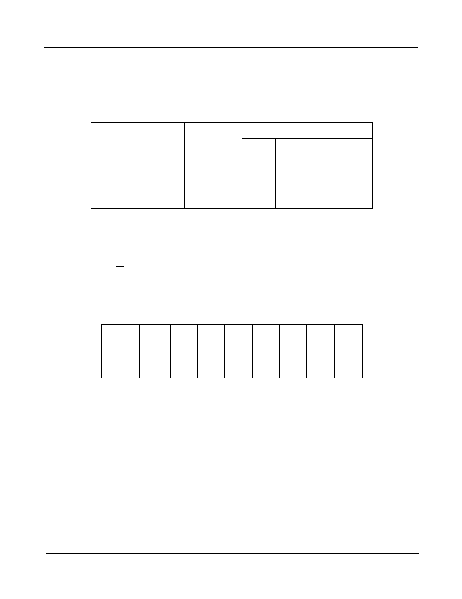
Pin Listings
No.
Name
No.
Name
No.
Name
No.
Name
1
QDC
11
SLEEP
21
PUMP
31
RFIN
2
QDC
12
SCL
22
N/C
32
RFIN
3
QOUT
13
SDA
23
Vvar
33
N/C
4
QOUT
14
XTAL
24
P0
34
RFAGC
5
VccBB
15
XTALCAP
25
LOCK
35
PTEST
6
VccBB
16
ADD
26
VccRF
36
VccLO
7
IOUT
17
DIGDEC
27
RFBYPASS
37
VccLO
8
IOUT
18
VccDIG
28
RFBYPASS
38
LOTEST
9
IDC
19
VccTUNE
29
VccRF
39
P1
10
IDC
20
DRIVE
30
N/C
40
CNT
Table 1 - Pins by Number Order
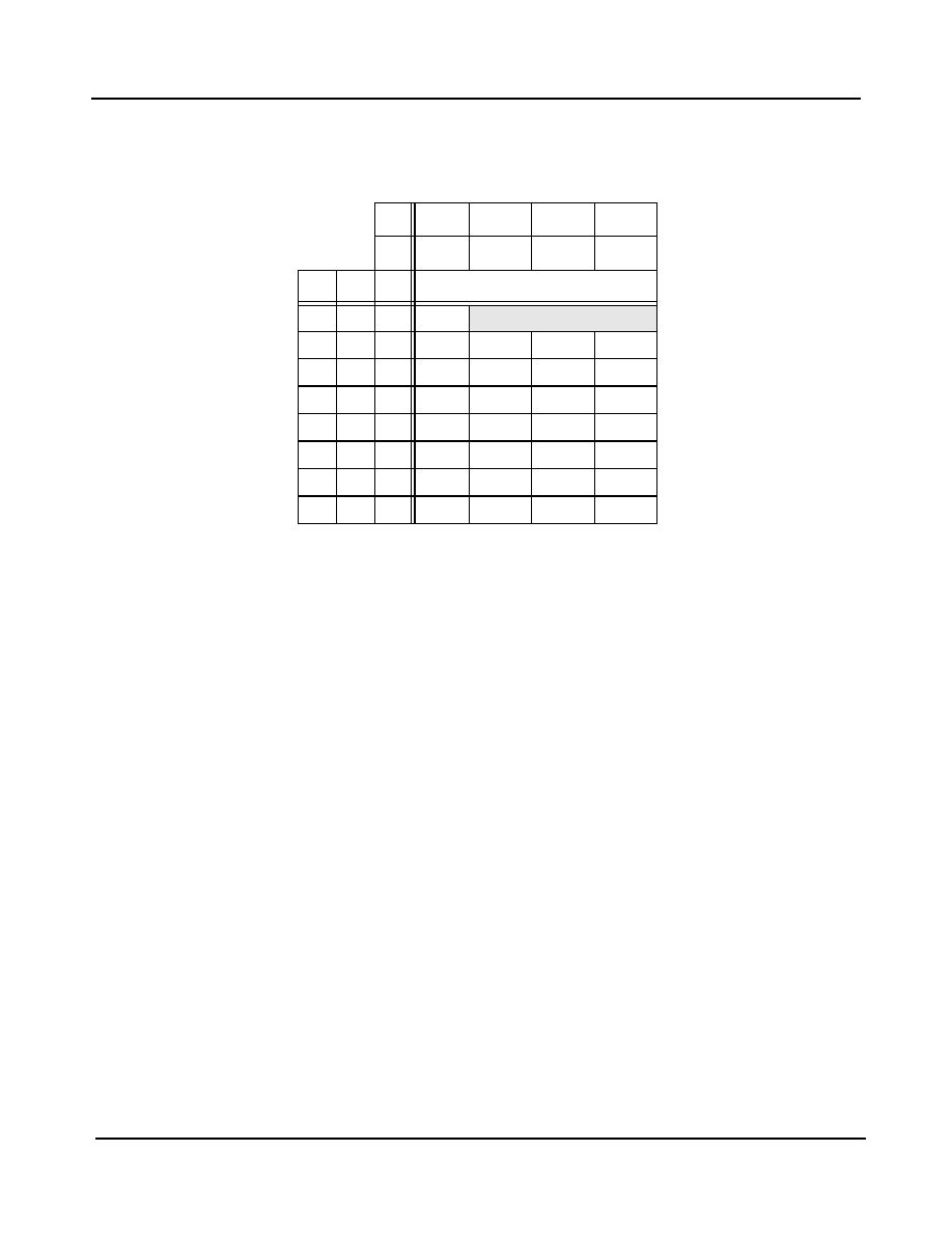
Name
No.
Name
No.
Name
No.
Name
No.
ADD
16
N/C
22
QOUT
4
VccBB
6
CNT
40
N/C
30
RFAGC
34
VccDIG
18
DIGDEC
17
N/C
33
RFIN
31
VccLO
36
DRIVE
20
P0
24
RFIN
32
VccLO
37
IDC
9
P1
39
RFBYPASS
27
VccRF
26
IDC
10
PTEST
35
RFBYPASS
28
VccRF
29
IOUT
7
PUMP
21
SCL
12
VccTUNE
19
IOUT
8
QDC
1
SDA
13
Vvar
23
LOCK
25
QDC
2
SLEEP
11
XTAL
14
LOTEST
38
QOUT
3
VccBB
5
XTALCAP
15
Table 2 - Pins by Name Order
ZL10036
Data Sheet
8
Zarlink Semiconductor Inc.
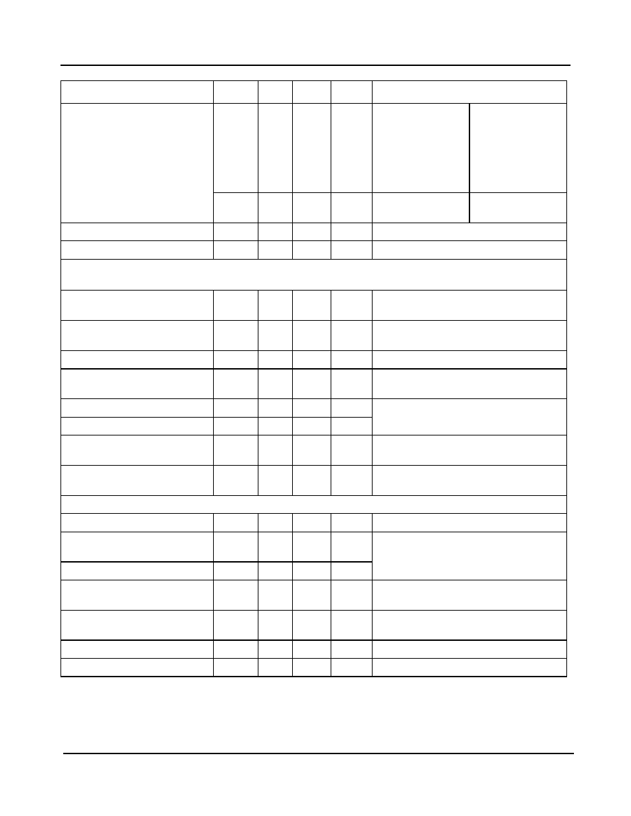
Pin Description
Pin
Symbol
Direction
Function
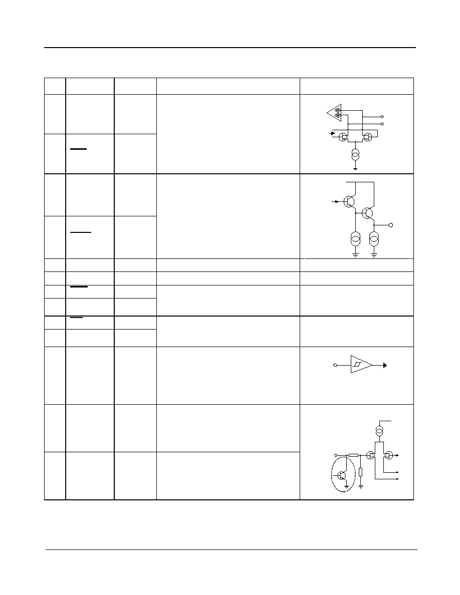
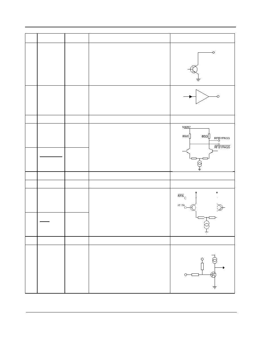
Schematics
1
QDC
NA
Q Channel DC offset correction
capacitor. Configuration and value as per
application diagram (see Figure 2)
2
QDC
NA
3
QOUT
Out
Q Channel baseband differential outputs.
AC couple outputs as per applications
diagram (see Figure 2)
4
QOUT
Out
5
VccBB
+5 V voltage supply for Baseband
6
VccBB
+5 V voltage supply for Baseband
7
IOUT
Out
I Channel baseband differential outputs
AC couple outputs as per applications
diagram (Figure 2)
Same configuration as pins 3 &
4
8
IOUT
Out
9
IDC
NA
I Channel DC offset correction capacitor.
Configuration and value as per
application diagram (Figure 2)
Same configuration as pins 1 &
2
10
IDC
NA
11
SLEEP
In
Hardware power down input.
Logic `0' � normal mode.
Logic `1' - analogue sections are
powered down.
This function is OR'ed with the PD
control function, see section 3.1.2
12
SCL
In
I�C serial clock input
13
SDA
Out
I�C serial data input/output
10
�A
Internal
Baseband
Signal
DC
Correction
10
�A
Internal
Baseband
Signal
Internal
Baseband
Signal
DC
Correction
DC
Correction
Output
1.2 mA
VccBB
Output
1.2 mA
VccBB
CMOS Digital Input
SLEEP
CMOS Digital Input
SLEEP
DIGDEC
500k
500k
SDA/SCL
Input
SDA
only
DIGDEC
500k
500k
SDA/SCL
Input
SDA
only

ZL10036
Data Sheet
9
Zarlink Semiconductor Inc.
14
XTAL
In
Reference oscillator crystal inputs.
Selected crystal frequency must be
programmed in BR4 to BR0 for correct
baseband filter bandwidth operation.
XTAL pin is used for external reference
input via 10 nF capacitor.
15
XTALCAP
Out
16
ADD
In
Variable I�C address selection allowing
the use of more than one device per I�C
bus system by the voltage on this pin.
See Table 3 for programming details.
17
DIGDEC
Out
Decouple pin for internal digital 3.3 V
regulator
18
VccDIG
+5 V voltage supply for digital logic
19
VccTune
Varactor tuning +5 V supply
20
DRIVE
IO
Loop amplifier output and input pins
21
PUMP
IO
22
N/C
Not connected. Ground externally.
23
Vvar
In
LO tuning voltage input
Pin
Symbol
Direction
Function
Schematics
XTAL
XTALCAP
0.2mA
100
DIGDEC
400
XTAL
XTALCAP
0.2mA
100
DIGDEC
400
20k
60k
ADD
Input
DIGDEC
20k
60k
ADD
Input
DIGDEC
DIGDEC
VccDIG
DIGDEC
VccDIG
DRIVE
3K
PUMP
CPDEC
VccTUNE
DRIVE
3K
PUMP
CPDEC
VccTUNE
Vvar
1 k
Vbias
Vvar
1 k
Vbias
ZL10036
Data Sheet
10
Zarlink Semiconductor Inc.
24
P0
Out
Switching port P0.
`0' = disabled (high impedance).
`1' = enabled.
25
LOCK
Out
Output which indicates that phase
comparator phase and frequency lock
has been obtained and that the varactor
voltage is within `tune unlock' window.
This powers up in logic `0' state.
26
VccRF
+5 V voltage supply for RF
27
RFBYPASS
Out
RF Bypass differential outputs.
AC couple outputs. Matching circuitry as
per applications diagram (Figure 2).
In applications where RF Bypass is not
required, pins should not be connected.
28
RFBYPASS
Out
29
VccRF
+5 V voltage supply for RF
30
N/C
Not connected. Ground externally.
31
RFIN
In
RF differential inputs.
AC couple input.
Matching circuitry as per applications
diagram.
32
RFIN
In
33
N/C
Not connected. Ground externally.
34
RFAGC
In
RF analogue gain control input
Pin
Symbol
Direction
Function
Schematics
P0/P1
P0/P1
LOCK
CMOS Digital Output
LOCK
CMOS Digital Output
VccRF
RFAGC
5k
20k
Vref
VccRF
RFAGC
5k
20k
Vref

ZL10036
Data Sheet
11
Zarlink Semiconductor Inc.
1.0 Overview
1.1 Conventions in this Manual
Hexadecimal values are typically shown as 0xABCDEF. Binary values (usually of register bits) are shown as
01100
2
. All other numbers should be considered to be decimal values unless specified otherwise.
35
PTEST
In
Connected to internal circuit for
monitoring die temperature
36
VccLO
+5 V voltage supply for LO
37
VccLO
+5 V voltage supply for LO
38
LOTEST
IO
Bi-directional test port for accessing
internal LO
AC couple input.
39
P1
Out
Switching port P1
`0' = disabled (high impedance)
`1' = enabled
Same configuration as pin 24,
P0
40
CNT
Bonded to paddle. Production continuity
test for paddle soldering
Note: Exposed paddle on rear of package must be connected to GND
Pin
Symbol
Direction
Function
Schematics
PTEST
PTEST
LOTEST
VccLO
Bias
LOTEST
VccLO
Bias

ZL10036
Data Sheet
12
Zarlink Semiconductor Inc.
2.0 Functional Description
Figure 3 - Functional Block Diagram
2.1 Quadrature Down-Converter
In normal applications the tuner RF input frequency of 950 - 2150 MHz is fed directly to the ZL10036 RF input
preamplifier stage, through an appropriate impedance match. The input preamplifier is optimized for NF, S11 and
signal handling.
The signal handling of the front end is designed such that no tracking filter is required to offer immunity to input
composite overload.
2.2 AGC Functions
The ZL10036 contains an analogue RF AGC combined with digitally controlled gain for RF, baseband pre-filter and
post-filter, as described in Figure 4. The baseband AGC is controlled by the I�C bus and is divided into pre- and
post-baseband filter stages, each of which have 12.6 dB of gain adjust in 4.2 dB steps.
The RF AGC is provided as the dynamic system gain adjust under control of the baseband analogue AGC output
function whereas the digitally controlled gains are provided to maximize performance under different signal
conditions. The total AGC gain range will guarantee an operating dynamic range of -92 to -10 dBm.
The digitally controlled RF gain adjust and the baseband pre-filter stage can be adjusted in sympathy to maintain a
fixed overall conversion gain. The lower RF gain setting would be used in situations where for example there is a
high degree of cable tilt or high desired to undesired ratio, whereas the higher RF gain setting would be used in
situations where for example it is desirable to minimize NF.

ZL10036
Data Sheet
13
Zarlink Semiconductor Inc.
The baseband post-filter gain stage can be used to provide additional gain to maintain desired output amplitude
with lower symbol rate applications.
Figure 4 - AGC Control Structure
2.2.1 RF
The RF input amplifier feeds an AGC stage, which provides for RF gain control.
Figure 5 - Typical First Stage RF AGC Response
The RF AGC is divided into two stages. The first stage is a continually variable gain control stage, which is
controlled by the AGC sender and provides the main system AGC set under control of the analogue AGC signal
generated by the demodulator section. The second stage is a bus programmable, two position gain set previous to
the quadrature mixer and provides for 4 dB of gain adjust under software control.
The analogue RF AGC is optimized for S/N and S/I performance across the full dynamic range. The RF AGC
characteristic, variation of IIP2, IIP3 and NF are contained in Figure 6, Figure 7 & Figure 8 respectively.
The RF preamplifier is also coupled to the selectable RF bypass, which is described in "RF bypass" on page 16.
The specified electrical parameters of the RF input are unaffected by the RF bypass state.
Normalized gain
range in dB:
0 - 72
0 or +4
0 to 12.6 in 4.2 dB steps
0 to 12.6 in 4.2 dB steps
Gain function:
RF AGC
Stepped
Stepped
Stepped
Control
function:
Analogue
voltage
I�C bus
I�C bus
I�C bus
-80
-70
-60
-50
-40
-30
-20
-10
0
10
0
0.5
1
1.5
2
2.5
3
3.5
4
4.5
5
AGC control voltage V
Co
n
versio
n
g
a
in
relat
i
ve t
o
max g
a
in
(
d
B)
ZL10036
Data Sheet
14
Zarlink Semiconductor Inc.
Figure 6 - Variation in IIP2 with AGC setting
(RF gain adjust = +0 dB, prefilter = +4.2 dB and postfilter = 4.2 dB, baseband filter bandwidth = 22 MHz)
Figure 7 - Variation in IIP3 with AGC setting
(RF gain adjust = +0 dB, prefilter = +4.2 dB and postfilter = 4.2 dB, baseband filter bandwidth = 22 MHz)
-10
-5
0
5
10
15
20
25
30
35
10
20
30
40
50
60
70
80
Gain setting dB
IIp
2
d
B
m
-50
-40
-30
-20
-10
0
10
20
20
30
40
50
60
70
80
Gain setting dB
IIP3
d
B
m

ZL10036
Data Sheet
15
Zarlink Semiconductor Inc.
Figure 8 - Variation in NF with Input Amplitude (typical)
The output of the RF AGC stage is coupled to the quadrature mixer where the RF input is mixed with quadrature LO
(local oscillator) signals generated by the on-board LO.
2.2.2 Baseband
The mixer outputs are coupled to the baseband quadrature channel amplifier and filter stage, which is of 7th order
topology. Operation and control of the baseband filter is contained in "Baseband Filter" on page 17.
The baseband paths are DC coupled, and include a DC correction loop. The high pass characteristic for the DC
correction loop is defined by the off chip capacitor connected to pins `IDC/IDC' and `QDC/QDC'. The output of each
channel stage is designed for low impedance drive capability and low intermodulation and can be loaded either
differentially or single-ended; in the case of single-ended load the unused output should be unloaded. The
maximum output load is defined in the electrical characteristics table.
0
10
20
30
40
50
60
-90
-80
-70
-60
-50
-40
-30
-20
-10
0
Input Amplitude (dBm)
NF
(
d
B)
RF programmable gain = 4 dB , prefilter gain = 4.2 dB, po st filter gain = 0 dB
B aseband o utput level = 0.5 Vp-p

ZL10036
Data Sheet
16
Zarlink Semiconductor Inc.
2.3 RF bypass
The ZL10036 provides an independent bypass function, which can be used for driving a second receiver module.
The electrical characteristics of the RF input are unchanged by the state of the RF bypass.
The bypass provides a differential buffered output from the input signal with a nominal 3.5 dB gain. The unused
output should be terminated as in Figure 2 on page 2.
The bypass function is enabled by a single register bit and is not disabled by either the PD bit or the SLEEP pin.
When disabled the bypass function is in a `power-down' state. On power up the bypass function is enabled.
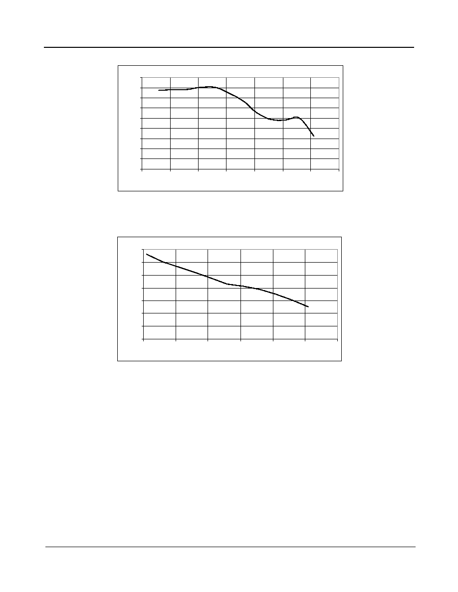
Figure 9 - RF input and Output (bypass) Return Losses
-30
-25
-20
-15
-10
-5
0
900 1000 1100 1200 1300 1400 1500 1600 1700 1800 1900 2000 2100 2200
Frequency (MHz)
R
e
tu
r
n
L
o
ss (d
B
)
S11 RFBypass On
S22 RFBypass On

ZL10036
Data Sheet
17
Zarlink Semiconductor Inc.
2.4 Baseband Filter
The filter bandwidth is controlled by a Frequency Locked Loop (FLL) the timing of which is derived from the
reference crystal source by a reference divider. Five control bits set the system reference division ratio and the
baseband filter bandwidth can be programmed with a further six control bits for a nominal range of 4 - 40MHz
1
.
Figure 10 - Normalized Filter Transfer Characteristic (Setting 20 MHz)
The -3 dB bandwidth of the filter (Hz) is given by the following expression:
Where:
f
-3dB
= Baseband filter �3 dB bandwidth (Hz) which should be within the range
.
f
xtal
= Crystal oscillator reference frequency (Hz).
K = 1.257 (constant).
BF = Decimal value of the register bits BF6:BF1, range 0 - 62.
BR = Decimal value of the bits BR4:BR0 (baseband filter reference divider ratio), range 4 - 27.
= 575 kHz to 2.5 MHz.
Methods for determining the values of BR and BF are given in the section on software, please see 4.3, "Symbol
Rate and Filter Calculations" on page 26.
1. specification compliant over the range 8 - 35 MHz.
Normalised Filter Response (20MHz filter setting)
-100
-80
-60
-40
-20
0
0.1
1
10
100
f/fc
Normalised Amplitude (dB)
f
-3dB
f
xtal
BR
----------
BF 1
+
(
)
1
K
----
�
�
=
8MHz
f
3dB
�
35MHz
f
xtal
BR
---------

ZL10036
Data Sheet
18
Zarlink Semiconductor Inc.
2.5 Local Oscillator
The LO on the ZL10036 is fully integrated and consists of three oscillator stages. These are arranged such that the
regions of operation for optimum phase noise are contiguous over the required tuning range of 950 to 2150 MHz
and over the specified operating ambient conditions and process spread.
The local oscillators operate at a harmonic of the required frequency and are divided down to the required LO
conversion frequency. The required divider ratio is automatically selected by the LO control logic, hence
programming of the required conversion frequency across the oscillator bands is automatic and requires no
intervention by the user.
Figure 11 - LO Phase Noise Performance
The oscillators are designed to deliver good free running phase noise at 10 kHz offset, therefore the required
integrated phase jitter from the LO can be achieved without the requirement for running with a high comparison
frequency and hence large tuning increment and wide loop bandwidth.
2.6 PLL Frequency Synthesizer
The PLL frequency synthesizer section contains all the elements necessary, with the exception of a frequency
reference and loop filter to control a varicap tuned LO, so forming a complete PLL frequency synthesized source.
The device allows for operation with a high comparison frequency and is fabricated in high speed logic, which
enables the generation of a loop with good phase noise performance. The loop can also be operated up to
comparison frequencies of 2 MHz enabling application of a wide loop bandwidth for maximizing the close in phase
noise performance. The LO conversion frequency is coupled to the 15-bit divider in the PLL frequency synthesizer.
The output of the programmable divider is fed to the phase comparator where it is compared with the comparison
frequency. This frequency is derived either from the on-board crystal controlled oscillator or from an external
reference source. In both cases the reference frequency is divided down to the comparison frequency by the
reference divider, which is programmable into one of 29 ratios as detailed in Table 13 on page 25.
The typical application for the crystal oscillator is contained in Figure 2 on page 2. The output of the phase detector
feeds a charge pump and loop amplifier section. This combined with an external loop filter integrates the current
pulses into the varactor line voltage with an output range of Vee to VccTUNE. The varactor line voltage is externally
coupled to the oscillator section through the input Vvar, enabling application of a third order loop.
Control of the charge pump current can be made as described in Table 12 on page 24.
-150
-140
-130
-120
-110
-100
-90
-80
-70
-60
10
100
1000
10000
100000
Frequency offset (log (offset in kHz))
P
h
ase n
o
i
se (d
Bc/Hz)

ZL10036
Data Sheet
19
Zarlink Semiconductor Inc.
2.7 Control Logic
The ZL10036 is controlled by an I�C data bus and can function as a slave receiver or slave transmitter compatible
with 3V3 or 5 V levels.
Data and Clock are input on the SDA and SCL lines respectively as defined by I�C bus standard. The device can
either accept data (slave receiver, write mode), or send data (slave transmitter, read mode). The LSB of the
address byte (R/W) sets the device into write mode if it is logic `0', and read mode if it is logic `1'. Table 4 and Table
6 illustrate the format of the read and write data respectively. The device can be programmed to respond to one of
four addresses, which enables the use of more than one device in an I�C bus system if required for use in PVR
1
systems, for example. Table 3 shows how the address is selected by applying a voltage to the address, `ADD',
input. When the device receives a valid address byte, it pulls the SDA line low during the acknowledge period, and
during following acknowledge periods after further data bytes are received. When the device is programmed into
read mode, the controller accepting the data must pull the SDA line low during all status byte acknowledge periods
to read another status byte. If the controller fails to pull the SDA line low during this period, the device generates an
internal STOP condition, which inhibits further reading.
All the ZL10036 functions are controlled by register bits written through the I�C bus interface. The SLEEP pin can
be used to power-down the device, but it can also be put into the power-down mode with the PD register bit, the two
functions being logically OR'ed.
Feedback on the status of the ZL10036 is provided through eight bits in the status byte register, and the phase lock
state is also available on the LOCK output pin (as well as the FL register bit).
3.0 User Control
3.1 I/O Pins
The I�C interface controls all the major functions in the ZL10036. Apart from the various analogue functions, the
only pins that either control the ZL10036, or are controlled by the internal logic, are the LOCK, SLEEP, P1, P0 and
ADD pins. Details follow:
3.1.1 LOCK - Pin 25
This is an output which indicates phase frequency lock for optimum phase noise. The CMOS output can directly
drive a low power LED if required.
3.1.2 SLEEP - Pin 11
The SLEEP pin shuts down the analogue sections of the device to give a considerable power saving, typically
reducing the power to about one third of its normal level. The RF-bypass function is entirely separate and is
unaffected by the state of this pin. The SLEEP pin's function is OR'ed with the PD register bit see 3.4.9, "Power
Down (PD Bit)" on page 24, so that if either is a logic one, the ZL10036 will be powered down, or alternatively, both
must be at logic zero for normal operation.
3.1.3 Output Ports, P1 & P0 - Pins 39 & 24
Two open-collector ports are provided for general purpose use, under control of register bits P1 and P0. The default
at power-up is for the P1 & P0 register bits to be low, hence the outputs will be off, i.e., in their high-impedance
states. If connected to a pull-up resistor this will therefore result in a logic high. Setting a register bit high will turn
the corresponding output on and therefore pull the logic level to near 0 V giving a logic low.
1. PVR - Personal Video Recorder where dual tuners allow the viewer to watch one channel and record another simultaneously, usually to a
hard-disk recording system.
ZL10036
Data Sheet
20
Zarlink Semiconductor Inc.
3.2 Device Address Selection
Two internal logic levels, MA1 and MA0, can be set to one of four possible logic states by the voltage applied to the
ADD pin (#16). These four states in turn define four different read and write addresses on the I�C bus, so that as
many as four separate devices can be individually addressed on one bus. This is of particular use in a multi-tuner
environment as required by PVR applications.
3.3 Read Register
The ZL10036 status can be read by addressing the device in its slave transmitter mode by setting the LSB of the
address byte (the R/W bit) to a one. After the master transmits the correct address byte, the ZL10036 will
acknowledge its address, and transmit data in response to further clocks on the SCL input. If the master responds
with an acknowledge and further clocks, the status byte will be retransmitted until such time as the master fails to
send an acknowledge, when the ZL10036 will release the data bus, allowing the master to generate a stop
condition.
The individual bits in the status register have the following meanings:
3.3.1 Power-On Reset Indicator (POR bit)
This bit is set to a logic `1' if the VccDIG supply to the PLL section has dropped below typically 3.6 V, e.g., when the
device is initially turned on. The bit is reset to `0' when the read sequence is terminated by a STOP command.
When the POR bit is high, this indicates that the programmed information may have been corrupted and the device
reset to power up condition.
3.3.2 Frequency & Phase Lock (FL bit)
Bit 6 (FL) indicates whether the synthesizer is phase locked, a logic `1' is present if the device is locked, and a logic
`0' if the device is unlocked.
ADD Pin Voltage
MA1
MA0
Write Address
Read Address
Hex.
Dec.
Hex.
Dec.
Vee (0 V or Gnd)
0
0
0xC0
192
0xC1
193
Open circuit
0
1
0xC2
194
0xC3
195
0.5 * DIGDEC (�20%)
1
1. can be programmed with a single 30 k
resistor to DIGDEC
1
0
0xC4
196
0xC5
197
DIGDEC
1
1
0xC6
198
0xC7
199
Table 3 - Address Selection
Bit No.
7
(MSB)
6
5
4
3
2
1
0
(LSB)
Address
1
1
0
0
0
MA1
MA0
1
Status
POR
FL
X
X
X
X
X
X
Table 4 - Read Data Bit Format (MSB is Transmitted First)

ZL10036
Data Sheet
21
Zarlink Semiconductor Inc.
3.3.3 Internal Operation Indicators (X Bits)
These bits indicate internal logic states and are not required for normal use of the ZL10036.
3.4 Write Registers
The ZL10036 has twelve registers which can be programmed by addressing the device in its slave receiver mode,
setting the LSB of the address byte (the R/W bit) to a zero. After the master transmits the correct address byte, the
ZL10036 will acknowledge its address, and accept data in response to further clocks on the SCL line. At the end of
each byte, the ZL10036 will generate the acknowledge bit. The master can at this point, generate a stop condition,
or further clocks on the SCL line if further registers are to be programmed. If data is written after the twelfth register
(byte-13), it will be ignored.
3.4.1 Register Sub-Addressing
If some register bits require changing, but not all, it is not necessary to write to all the registers. The registers can be
addressed in pairs starting with the even numbered bytes, i.e., 2 & 3, 4 & 5, etc. Table 5 below shows the protocol
required to address any of the even numbered register bytes. It therefore follows that to write to register byte-7 for
instance, byte-6 must also be written first. Register pairs may be written in any order, as required by the software,
e.g., 10/11 may be followed by 4/5.
Data Bits
Byte Selected
7
(MSB)
6
5
4
0
X
X
X
2
1
0
X
X
4
1
1
0
0
6
1
1
0
1
8
1
1
1
0
10
1
1
1
1
12
`X' = Don't care (content defines a register bit).
Table 5 - Byte Address Allocation in Write Mode

ZL10036
Data Sheet
22
Zarlink Semiconductor Inc.
3.4.2 Register Mapping
Byte
Bit No.
Function
7
(MSB)
6
5
4
3
2
1
0
(LSB)
Reset
state
(hex.) 1
1. This is the power-on default register value - recommended operating values may be different, see "4.1" on page 26.
Further information
1
Device address
1
1
0
0
0
MA1 MA0
0
Table 3 on page 20
2
Programmable
Divider
0
2
14
2
13
2
12
2
11
2
10
2
9
2
8
0x00
See 3.4.3 on page 23
3
2
7
2
6
2
5
2
4
2
3
2
2
2
1
2
0
0x00
4
Control Data
1
0
RFG
BA1
BA0 BG1 BG0 LEN
0x80
"3.4.4" to "3.4.7" on p. 24
5
P0
C1
C0
R4
R3
R2
R1
R0
0x00
pp. 24, 24 & 25
6
1
1
0
0
RSD
0
0
0
0xC0
see "3.4.13" on page 25
7
P1
BF6
BF5
BF4
BF3
BF2 BF1
0
0x20
pp. 24 & 25
8
1
1
0
1
0
0
1
1
0xDB
page 26
9
0
0
1
1
0
0
0
0
0x30
page 26
10
1
1
1
0
0
0
0
1
0xE1
page 26
11
U
2
2. This bit is undefined at power up as its level determines different functions for the other bits in this register.
1
1
1
0
1
0
1
0x75/F5
page 26
12
1
1
1
1
0
0
0
0
0xF0
test function only
13
PD
BR4
BR3
BR2
BR1 BR0 CLR
TL
0x28
pp. 24, 25 & 25
Table 6 - Bit Allocations in the Write Registers
Symbol
Definition
Symbol
Definition
2
14
-2
0
Programmable division ratio control bits
MA1,MA0 Variable address bits
BA1-0
Baseband prefilter gain adjust
P0, P1
External switching ports
BF6-1
Baseband bandwidth adjust
PD
Power down
BG1-0
Baseband postfilter gain adjust
R4-R0
Reference division ratio select
BR4-0
Baseband filter FLL reference frequency select RFG
RF programmable gain adjust
C1,C0
Charge pump current select
RSD
Resistor switch disable
CLR
Control logic reset
TL
Buffered LO output select
LEN
RF bypass enable
Table 7 - Key to Table 6

ZL10036
Data Sheet
23
Zarlink Semiconductor Inc.
3.4.3 Synthesizer Division Ratio (2
14
:2
0
Bits)
The PLL synthesizer interfaces with the LO multiplex output and runs at the desired frequency for down-conversion.
The step size at the desired conversion frequency, is equal to the loop comparison frequency.
The programmable division ratio, 2
14
to 2
0
, required for a desired conversion frequency, can be calculated from the
following formula:
Desired conversion frequency =
where:
f
step
= Fcomp
3.4.4 RF Gain (RFG Bit)
The RF gain is programmed by setting the RFG bit, bit-5 of register byte-4 as required. See also Figure 4, "AGC
Control Structure" on page 13.
3.4.5 Baseband Pre-Filter Gain Adjust (BA1:0 Bits)
The baseband pre-filter gain is programmed by setting BA1:0, bits-4 & 3 of register byte-4 as required. See also
Figure 4, "AGC Control Structure" on page 13.
3.4.6 Baseband Post-Filter Gain (BG1:0 Bits)
The baseband post-filter gain is programmed by setting BG1:0, bits-2 & 1 of register byte-4 as required. See also
Figure 4, "AGC Control Structure" on page 13.
RFG
Gain Adjust (dB)
0
0 (reset
state)
1
+4
Table 8 - RFG Register Bit Function
BA1
BA0
Pre-Filter Gain Adjust (dB)
0
0
0.0
(reset state)
0
1
+4.2
1
0
+8.4
1
1
+12.6
Table 9 - BA1/0 Register Bits Function
BG1
BG0
Post-Filter Gain Adjust (dB)
0
0
0.0
(reset state)
0
1
+4.2
1
0
+8.4
1
1
+12.6
Table 10 - BG1/0 Register Bits Function
f
step
2
14
2
13
2
12
2
2
2
1
+
2
0
+
+
+
(
)
�

ZL10036
Data Sheet
24
Zarlink Semiconductor Inc.
3.4.7 RF Bypass Disable (LEN Bit)
The RF bypass function is disabled by setting LEN, bit-0 of register byte-4 to a logic `1'. By default, this bit is at a
logic `0' at power-up, and therefore the function is enabled. If the function is not required, a power saving of
approximately 15% can be made by setting this bit. See also section 2.3 on page 16.
3.4.8 Output Port Controls (P1 & P0 Bits)
Register bits P1 and P0, bit-7 in register bytes-7 & 5 respectively, control the output port pins, P1 & P0, pin numbers
39 & 24 respectively.
3.4.9 Power Down (PD Bit)
Bit-7 of byte-13 controls the PD register bit which is an alternative to the SLEEP pin (see "SLEEP - Pin 11" on
page 19). Setting the PD bit to a logic `1' shuts down the analogue sections of the ZL10036 effecting a saving of
about two thirds of the power required for normal operation. A logic '0' restores normal operation. With either
hardware or software power-down, all register settings are unaffected.
3.4.10 Logic Reset (CLR Bit)
Bit-1 of byte-13 controls the CLR register bit. When set to a logic `1', this self-clearing bit resets the ZL10036 control
logic. Writing a logic `0' has no effect. The following register numbers are reset to their power-on state: 7, 9, 10, 11,
12 & 13. All other register's contents are unaffected.
3.4.11 Charge Pump Current (C1 & C0 Bits)
Register bits C1 and C0 are programmed by setting bits-6 & 5 of register byte-5. These bits determine the charge
pump current that is used on the output of the frequency synthesizer phase detector.
Bit P1 or P0
Port State
Logic State
(if connected to a pull-up)
0
High impedance
1
(reset state)
1
Low impedance to Vee (Gnd)
0
Table 11 - Port Control Bits
C1
C0
Current in �A
Min.
Typ.
Max.
0
0
�160
�210
�290
(reset state)
0
1
�280
�365
�510
1
0
�470
�625
�860
1
1
Not allowed
Table 12 - Charge Pump Currents
ZL10036
Data Sheet
25
Zarlink Semiconductor Inc.
3.4.12 Reference Division Ratios (R4:0 Bits)
Register bits R4:0 control the reference divider ratios as shown in Table 13. They are programmed through bit-4 to
bit-0 respectively, in byte-5.
3.4.13 Baseband Filter Resistor Switching (RSD)
The baseband filters use a resistor switching technique that improves bandwidth and phase matching between the
I and Q channels. The bandwidth range is effectively separated into 3 sub-ranges with different resistor values
being used in each sub-range. It is possible for the filter bandwidth accuracy to be degraded if the bandwidth setting
happens to coincide with one of the two transition points between these regions. This can be overcome by disabling
the resistor switching using the RSD bit. For optimum filter performance the RSD bit should first be enabled so that
the correct resistor value is automatically set for the selected bandwidth.
The RSD bit (bit-3 of byte-6) controls the resistor switching. With the default setting of logic '0' it is enabled and the
correct resistor value automatically chosen. With the RSD bit set to a logic '1' then the switching is disabled and this
freezes the resistors at their chosen value. The procedure when selecting a new bandwidth setting is to enable then
disable the switching; set RSD to logic '0' then to logic '1'.
3.4.14 Baseband Filter Bandwidth (BF6:1 & BR4:0 Bits)
Bits 6 to 1 of byte-7 configure bits BF6 to BF1 respectively. These bits set a decimal number in the range 0 to 62
(63 is not allowed) to determine the baseband filter bandwidth in conjunction with other values.
Bits 6 to 2 of byte-13 configure bits BR4 to BR0 respectively. These bits set the reference divider ratio for the
baseband filter. A number in the range 4 to 27 inclusive (values outside this range are not allowed) can be set, with
the proviso that the value of f
xtal
/BR4:0 must also be in the range 575 kHz to 2,500 kHz.
For further details, please also see 2.4, "Baseband Filter" on page 17 and "Symbol Rate and Filter Calculations"
(sect. 4.3) on page 26.
3.4.15 LO Test (TL Bit)
For test purposes, the LO clock divided by the prescaler ratio can be output on the LOTEST pin by setting bit TL
(byte-13 bit-0) to a logic `1'. By default this output is off, i.e., the TL bit is at logic `0'.
R4
0
0
1
1
R3
0
1
0
1
R2
R1
R0
Division Ratios
0
0
0
2
Illegal states
0
0
1
4
5
6
7
0
1
0
8
10
12
14
0
1
1
16
20
24
28
1
0
0
32
40
48
56
1
0
1
64
80
96
112
1
1
0
128
160
192
224
1
1
1
256
320
384
448
Table 13 - Division Ratios Set with Bits R4 - R0

ZL10036
Data Sheet
26
Zarlink Semiconductor Inc.
4.0 Software
In normal operation, only initialization, channel (frequency) changes and symbol rates require programming
intervention. Note that the PLL comparison frequency is set by the crystal frequency divided by the PLL reference
divide ratio. In the following examples of register settings, binary values are frequently used, indicated as e.g.,
0110
2
.
4.1 Power-on Software Initialization
a. Bytes 2 + 3: 2
14
- 2
0
= desired channel frequency/PLL comparison frequency.
b. Byte 4: BA1:0 = 01
2
for initial baseband filter input level.
c. Byte 4: BG1:0 = 01
2
for target baseband filter output level.
d. Byte 4: LEN = 1 if the RF loop through is to be disabled.
e. Byte 5: R4:0 = PLL reference divider for desired comparison frequency.
f. Bytes 8 - 10: should be set to the following values: 0xD3, 0x40 & 0xE3 respectively.
g. Byte 11: this should be written twice with the following values:0x5B & 0xF9. The order in which these
values are written is not important.
h. Byte 13: BR4:0 = Crystal frequency in use (see also 4.3.3.1 on page 27).
4.2 Changing Channel
Bytes 2 + 3: 2
14
- 2
0
= Channel frequency/PLL comparison frequency.
4.3 Symbol Rate and Filter Calculations
4.3.1 Determining the Filter Bandwidth from the Symbol Rate
f
bw
= (
* symbol rate)/(2.0 * 0.8) +
f
offs
where:
= 1.35 for DVB or 1.20 for DSS, and is the roll-off of the raised-root cosine filter in the transmitter,
f
offs
is the total offset of the received signal due to all causes (LNB drift, synthesizer step size, etc) and is read back
from the demodulator (ZL10036),
and
f
bw
is the -3 dB roll-off of the filter for: 8 MHz
f
bw
35 MHz.
For low symbol rates, the energy content within the bandwidth of the filters reduces significantly so incrementing
the baseband post-filter gain helps recover the signal level for the demodulator.
N.B. During channel acquisition or re-acquisition, the filter must be set to its maximum value.

ZL10036
Data Sheet
27
Zarlink Semiconductor Inc.
4.3.2 Calculating the Filter Bandwidth
The -3 dB bandwidth of the filter (Hz) is given by the following expression:
Equation 1 -
Where:
f
bw
= Baseband filter �3 dB bandwidth (Hz) which should be within the range
.
f
xtal
= Crystal oscillator reference frequency (Hz).
K = 1.257 (constant).
BF = Decimal value of the register bits BF6:BF1, range 0 - 62.
BR = Decimal value of the bits BR4:BR0 (baseband filter reference divider ratio), range 4 - 27.
where: 575 kHz
2.5 MHz.
The digital nature of the control loop means that the filter bandwidth setting is quantized: the difference between the
desired filter bandwidth and the actual filter bandwidth possible due to discrete settings causes a bandwidth error.
In order to minimize this bandwidth error, the maximum filter bandwidth setting resolution is needed. From the limits
given above, the best resolution possible is 575 kHz/1.257 = 457.4 kHz. However if this resolution is used, the
maximum bandwidth with BF = 62 is only 28.82 MHz, below the maximum of 35 MHz. Therefore for filter
bandwidths greater than 28.82 MHz the resolution must be decreased. For filter bandwidths around 35 MHz the
resolution is typically reduced to 698 kHz/1.257 = 555.3 kHz.
4.3.3 Determining the Values of BF and BR
4.3.3.1 Calculating the Value of BR
The above description can be described mathematically as:
For
f
bw
28.82MHz,
Equation 2 -
.
For
f
bw
> 28.82MHz,
Equation 3 -
.
These equations can give non-integer results so rounding must be performed. The values for BR should be
rounded DOWN to the nearest integer this ensures that
will not be below 575 kHz and that the maximum
programmable bandwidth will not be below the desired bandwidth due to rounding.
4.3.3.2 Calculating the Value of BF
Equation 4 -
For non-integer values of BF, the result should be simply rounded to the nearest integer to give the value for BF6:1.
f
bw
f
xtal
BR
----------
BF 1
+
(
)
1
K
----
�
�
=
8MHz
f
bw
35MHz
f
xtal
BR
---------
BR
f
xtal
575kHz
--------------------
=
BR
f
xtal
f
bw
--------
62 1
+
(
)
�
1
K
----
�
=
f
xtal
BR
---------
BF
f
bw
f
xtal
-------- BR
�
K
�
1
�
=
=

ZL10036
Data Sheet
28
Zarlink Semiconductor Inc.
4.3.4 Filter Bandwidth Programming Examples
Example 1, conditions:
f
xtal
= 10.111MHz,
f
bw
= 9MHz
Because
f
bw
is below 28.2MHz, the value of BR can be evaluated with equation 2:
This result should be rounded down to 17 to ensure that the result is not below the 575 kHz limit. Using this value
for BR, equation 4 can be evaluated:
The result can be rounded to the nearest value, i.e., BF = 18.
Example 2, conditions:
f
xtal
= 10.111MHz,
f
bw
= 34.6MHz
In this case,
f
bw
is above 28.2MHz so using equation 3 to solve for BR:
Using equation 4, this time with the rounded-down value of 14 for BR:
Rounding to the nearest integer thus gives a value of 59 for BF.
4.4 Programming Sequence for Filter Bandwidth Changes
a. Byte 6: Set RSD = 0 to re-enable baseband filter resistor switching.
b. Byte 7: Set BF6:1 to the value derived in 4.3.3.2, "Calculating the Value of BF" on page 27.
c. Byte 6: Set RSD = 1 to disable baseband filter resistor switching. This must happen no sooner than a
certain time after (b.). This minimum time equals BR/(32 * f
xtal
) seconds, where BR is the decimal value of
byte BR and f
xtal
is the reference crystal frequency.
BR
f
xtal
575kHz
--------------------
10.111MHz
575kHz
------------------------------
17.583
=
=
=
BF
f
bw
f
xtal
-------- BR
�
K
�
1
�
9MHz
10.11MHz
--------------------------- 17
�
1.257
�
1
�
18.02285
=
=
=
BR
f
xtal
f
bw
--------
63
( )
�
1
K
----
�
10.111MHz
34.6MHz
------------------------------
63
( )
�
1
1.257
---------------
�
14.647
=
=
=
BF
f
bw
f
xtal
-------- BR
�
K
�
1
�
34.6MHz
10.11MHz
--------------------------- 14
�
1.257
�
1
�
59.227
=
=
=

ZL10036
Data Sheet
29
Zarlink Semiconductor Inc.
5.0 Application Notes
5.1 Thermal Considerations
Figure 12 - Copper Dimensions for Optimum Heat Transfer
Figure 13 - Paste Mask for Reduced Paste Coverage
The ZL10036 uses the 40-pin QFN package with a thermal `paddle' in the base, which has a very high thermal
conductivity to the die, as well as low electrical resistance to the Vee connections. The ZL10036 has a fairly high
power density, and if the excess heat is not efficiently removed, it will rapidly overheat beyond the 125�C limit, and
affect the performance or could even cause permanent damage to the device.
The paddle is designed to be soldered to a size-matched pad on the PCB (see Figure 13 on page 29) which is
thermally connected to an efficient heat sink. The heat sink can be as simple as an area of copper ground plane on

ZL10036
Data Sheet
30
Zarlink Semiconductor Inc.
the underside of the board, thereby reducing the system cost. To transfer the heat from the paddle to the underside
of the board, an array of 25 x 0�3 mm� vias are used between the topside pad, which will be soldered to the paddle,
and the ground plane on the underside of the board. It is also possible to use a smaller number of larger vias, e.g.
16 x 0�5 mm�, but this arrangement is marginally less efficient.
The area of copper in the ground plane must be at least 2,000 mm� for 1 oz copper. If 2 oz copper board is used or
if multiple ground planes are available, as with a four-layer board, the area could be reduced somewhat, but in
general it is better to have the maximum cooling possible, as reliability will always be enhanced if lower
temperatures are maintained.
While it is possible to use a paste mask that simply duplicates the aperture for the 4.15 mm sq. paddle, the quantity
of solder paste under the device can cause problems and it is preferable to reduce the coverage to a level between
50% and 80% of the area. The pattern shown in Figure 14 on page 30 reduces the coverage to approximately 60%,
which should reduce out-gassing from under the device and improve the stand-off height of the package from the
board.
A very useful publication giving further details is: "Application Notes for Surface Mount Assembly of Amkor�s
MicroLeadFrame (MLF) Packages" which can be found on: www.amkor.com
5.2 Crystal Oscillator Notes
The 10.111 MHz frequency recommended for the crystal, is chosen such that when used with the Zarlink ZL10312
demodulator, the system frequency is 91 MHz = 9 * 10.111 MHz (91 MHz > 2 * 45 Ms/s).
Figure 14 - Typical Oscillator Arrangement with Optional Output
Figure 15 - Typical Arrangement for External Oscillator
Component
4 MHz
10.111 MHz
C10
47 pF
100 pF
C11
47 pF
100 pF
C12*
10 pF
15 pF
* C12 may be replaced by a link to GND if crystal output is not required.
Table 14 - Crystal Capacitor Values for 4 MHz and 10.111 MHz Operation
(component numbering refers to the example schematic, Figure 2 on page 2)

ZL10036
Data Sheet
31
Zarlink Semiconductor Inc.
6.0 Electrical characteristics
6.1 Test Conditions
The following conditions apply to all figures in this chapter, except where notes indicate other settings.
Tamb = -10� to 85�C, Vee= 0 V, All Vcc supplies = 5 V�5%
RF gain adjust = +0 dB, prefilter = +4.2 dB and postfilter = 4.2 dB. RFG=0, BA1=0, BA0=1, BG1=0, BG0=1
These characteristics are guaranteed by either production test or design. They apply within the specified ambient
temperature and supply voltage unless otherwise stated.
6.2 Absolute Maximum Ratings
Parameter
Symbol
Min.
Max.
Unit
Notes
Supply voltage
VccBB, VccDIG, VccLO,
VccRF, VccTUNE
-0.3
5.5
V
w.r.t. Vee
Storage temperature
T
STG
-55
150
�C
Junction temperature
T
j
125
�C
Voltage on SDA & SCL
-0.3
6
V
Vcc = Vee to 5.25 V
Voltage on DRIVE
-0.3
VccTUNE+0.3
V
Voltage on RFIN, RFBYPASS
and inverted equivalents
-0.3
VccRF+0.3
V
Voltage on RFAGC
Voltage on Vvar
-0.3
VccLO+0.3
V
Voltage on LOTEST
Voltage on IOUT, QOUT, IDC,
QDC and inverted
equivalents
-0.3
VccBB+0.3
V
Voltage on P1
Voltage at DIGDEC
-0.3
3.6
V
Voltage on PUMP
-0.3
VccDIG+0.3
V
Voltage on SLEEP and P0
Voltage on ADD, XTAL,
XTALCAP and LOCK
-0.3
DIGDEC+0.3
V
Sink current, P0 or P1
20
mA
Each output
ESD protection, pins 31 &
32
1
1. ESD protection can be increased by adding a protection diode (D1) to the input circuit as shown in the application circuit (Figure 2).
0.5
kV
To Mil-std 883B
method 3015 cat1
pins 1-30, 33-40
2.0
kV

ZL10036
Data Sheet
32
Zarlink Semiconductor Inc.
6.3 Recommended Operating Conditions
6.4 DC Characteristics
Parameter
Symbol
Min.
Max.
Unit
Notes
Supply voltage
VccBB, VccDIG, VccLO, VccRF, VccTUNE
4.75
5.25
V
w.r.t. Vee
Operating temperature
T
OP
-10
85
�C
Pins
Characteristic
Min.
Typ.
Max.
Units
Conditions
Normal operating conditions
All Vcc pins:
5, 6, 18, 19,
26, 29, 36,
37
Supply current
RF bypass
filter b.w.
210
259
mA
disabled
minimum
228
281
mA
maximum
243
300
mA
enabled
minimum
261
322
mA
maximum
82
107
mA
disabled
sleep mode
115
mA
enabled
QOUT,
QOUT, IOUT,
IOUT: 3, 4, 7,
8
Output impedance
25
Single-ended
Output load
1
15
k
pF
Maximum load, which can be
applied to output,
single-ended. If operated
single ended unused output
should be unloaded
QDC, QDC,
IDC, IDC: 1,
2, 9, 10
Bias voltage
3.8
V
Output impedance
11
k
SCL, SDA:
12, 13
Input high voltage
2.3
5.5
V
Input low voltage
0
1
V
Input current
-10
10
�A
Input voltage =Vee to
VccDIG
Leakage current
10
�A
Input voltage = Vee to 5.5 V,
VccDIG=Vee
Hysteresis
0.4
V
SDA: 13
Output voltage
0.4
V
Isink = 3 mA
0.6
V
Isink = 6 mA
PUMP: 21
Charge pump
leakage
+-3
+-20
nA
Vpin = 1.8 V
Charge pump
current
Vpin = 1.8 V. See Table 12
on page 24

ZL10036
Data Sheet
33
Zarlink Semiconductor Inc.
6.5 AC Characteristics
DRIVE: 20
Max. voltage
VccTUNE-0.2
V
On-chip 3 kohm load resistor
to VccTUNE
Min. voltage
0.3
V
XTAL,
XTALCAP:
14, 15
Recommended
crystal E.S.R.
10
200
Parallel resonant crystal
Vvar: 23
Input current
-1
1
mA
Vee <= Vvar <= 1.7 V
(on-chip varactors forward
biased)
-25
25
�A
1.7 V <= Vvar <= Vcc
P0, P1: 24,
39
Sink current
10
mA
At Vport = 0.7 V
Leakage current
10
�A
Vport = Vcc
LOCK: 25
Low output voltage
0.5
V
Out of lock
at 1 mA
High output voltage
DigDec-0.5
V
In lock
Load current
1
mA
ADD: 16
Input high current
1
mA
Vin = DIGDEC
Input low current
-0.5
mA
Vin = Vee
SLEEP: 11
Input high voltage
2
3.6
V
Sleep enabled
Input low voltage
Vee
0.5
V
Normal mode
Input DC current
10
�A
Vin = Vee to DIGDEC
RFAGC: 34
Leakage current
-150
150
�A
Vee <= Vagc<= Vcc
LOTEST: 38
Output impedance
100
Bias voltage
3.3
V
Characteristic
Min.
Typ.
Max.
Units
Conditions
System (See
1
)
Noise figure, DSB
9
dB
At -70 dBm operating level
2
12
dB
At -60 dBm operating level
2
10
dB
At -70 dBm operating level
13
dB
At -60 dBm operating level
Variation in NF with RF gain
adjust
-1
dB/dB
Above �60 dBm operating level
2
See Figure 8 on page 15
Conversion gain
Maximum
Minimum
72
78
6
10
dB
dB
Vagc = 0.75 V
Vagc = 4.25 V
AGC control range
68
72
dB
AGC monotonic, Vagc from Vee to Vcc
Pins
Characteristic
Min.
Typ.
Max.
Units
Conditions

ZL10036
Data Sheet
34
Zarlink Semiconductor Inc.
System IM2
-35
-40
dBc
dBc
See
3
See
4
System IM3
-15
dBc
See
5
Variation in system second
order intermodulation intercept
-1
dB/dB
See Figure on page 14 and
6
Variation in system third order
intermodulation intercept
-1
dB/dB
See Figure 7 on page 14 and
7
Input compression
-10
-6
dBm
See
8
LO second harmonic
interference level
-50
-35
dBc
See
9
, all gain settings
LNA second harmonic
interference level
-35
-20
dBc
See
10
Quadrature gain match
-1
1
dB
Filter bandwidth settings 8-35 MHz, up to
0.8 x filter -3 dB bandwidth
Quadrature phase match
�3
deg
I & Q channel in band ripple
1
dB
Synthesizer and other spurii on
I & Q outputs
-30
dBc
All gain settings below 68 dB
-25
dBc
At maximum gain. Linearly interpolated
between max. and 68 dB gain, see
11
LO reference sideband spur
level on I & Q outputs
-40
dBc
Synthesizer phase detector comparison
frequency 500-2000 kHz
In band LO leakage to RF input
-65
dBm
Within RF band 950-2150 MHz
-55
dBm
Within RF band 30-950 MHz
RF bypass
Gain
1.5
5.5 dB
NF
10
13
dB
OPIP3
9
dBm
See
12
OPIP2
26
dBm
See
13
Output return loss
9
dB
Z
0
= 75
. See Figure 9 on page 16, with
output matching as in Figure 2 on page 2.
Bypass enabled or disabled.
Forward isolation
25
dB
950-2150 MHz
Single-ended to single-ended, bypass
disabled
Reverse isolation
25
dB
In band LO leakage
-65
dBm
Converter
Converter Input return loss (pins
RFIN & RFIN)
8
10
dB
Z
0
= 75
. See Figure 9 on page 16. With
input matching as in Figure 2 on page 2.
Bypass enabled or disabled.
Characteristic
Min.
Typ.
Max.
Units
Conditions
ZL10036
Data Sheet
35
Zarlink Semiconductor Inc.
LO SSB phase noise
-76
-96
dBc/Hz
dBc/Hz
@ 10 kHz offset
@ 100 kHz offset
Measured either, at
baseband output of
10 MHz, PLL loop
bandwidth circa
100 Hz, or at
LOTEST output.
Vvar > 3 V
-110
-132
dBc/Hz
dBc/Hz
@ 1 MHz offset
Noise floor.
14
Measured at
LOTEST output.
LO integrated phase jitter
3
deg
See Figure 11 on page 18 and
15
LOTEST output amplitude
200
mVp-p
Test output enabled into 50
Baseband Filters
(specifications apply with both single-ended and differential load unless otherwise stated)
Bandwidth
4
40
MHz
See 2.4, "Baseband Filter" on page 17.
Maximum load as specified
Bandwidth absolute tolerance
-5
+5
%
Filter bandwidth setting, fset, 8-35 MHz.
Slave oscillator enabled, see
16
Channel bandwidth match
-1
+1
%
Filter bandwidth settings 8-35 MHz
Characteristic response
All bandwidth settings, see Figure 10 on
page 17.
Channel gain match
Included in system gain match
Channel phase match
Output total harmonic distortion
-26
dBc
At 0.8 V p-p, single-ended. Maximum
load as specified
Output limiting
1.0
Vp-p
Level at hard clipping, single-ended.
Maximum load as specified
Synthesizer
Crystal frequency
4
20
MHz
See Table 14 on page 30.
External reference input
frequency
4
20
MHz
Sinewave coupled through 10nF blocking
capacitor to pin XTAL. XTALCAP is left
open.
External reference drive level
0.2
0.5 Vp-p
Phase detector comparison
frequency
31.25
2000
kHz
Equivalent phase noise at
phase detector
-148
dBc/Hz SSB, within loop bandwidth. Phase
detector comparison frequency = 1 MHz
LO division ratio
240
32767
Maximum SCL clock rate
100
kHz
1. All power levels are referred to 75
and assume an ideal impedance match: 0 dBm = 109 dBmV. System specifications refer to
total cascaded system of converter/AGC stage and baseband amplifier/filter stage with maximum terminating load as specified in "DC
Characteristics" on page 32, with output amplitude of 0.5 Vp-p differential.
2. See Figure 8, RF gain adjust = +4 dB, prefilter = +4.2 dB and postfilter = 0 dB, RFG = 1, BA1 = 0, BA0 = 1, BG1 = 0, BG0 = 0
Characteristic
Min.
Typ.
Max.
Units
Conditions

ZL10036
Data Sheet
36
Zarlink Semiconductor Inc.
3. 'Baseband defined IM2'. AGC set to deliver an output of 0.5 Vp-p with an input CW @ frequency fc of -25 dBm. Two undesired
tones at fc+146 and fc+155 MHz @ -11 dBm generating output intermodulation spur at 9 MHz. Baseband filter at 22 MHz bandwidth
setting.
4. 'Front end defined IM2'. LO set to 2145 MHz and AGC set to deliver a 5 MHz output of 0.5 Vp-p with a desired input CW @ fre-
quency 2150 MHz of -45 dBm. Sum IM2 product from two undesired tones at 1.05 and 1.1 GHz at -25 dBm converted to 5 MHz base-
band with desired input removed. Baseband filter at 22 MHz bandwidth setting.
5. 'IM3'. AGC set to deliver an output of 0.5 Vp-p with an input CW @ frequency fc of -30 dBm. Two undesired tones at fc+55 and
fc+105 MHz at -11 dBm generating output intermodulation spur at 5 MHz. Baseband filter at 22 MHz bandwidth setting.
6. 'Front end defined' variation in IP2 from two undesired tones at 1.05 and 1.1 GHz at 20 dBc relative to desired at 2.15 GHz con-
verted to 5 MHz baseband with LO tuned to 2.145 GHz with AGC set to deliver 0.5 Vp-p differential on desired, as desired amplitude
is varied from -45 dBm to -75 dBm.
7. Variation in IP3 product from two undesired tones at fc+55 and fc+105 MHz at 19 dBc relative to desired at fc converted to 5 MHz
baseband with LO tuned to desired at fc GHz with AGC set to deliver 0.5 Vp-p differential on desired, as desired amplitude is varied
from -30 dBm to -75 dBm.
8. AGC set to deliver an output of 0.5 Vp-p with an input CW @ frequency fc of -35 dBm. Input compression defined as the level of
interferer at 100 MHz offset, which leads to a 1 dB compression in gain.
9. The level of 2.01 GHz down converted to baseband relative to 1.01 GHz with the oscillator tuned to 1 GHz, measured with no input
pre-filtering.
10. The level of second harmonic of 1.01 GHz input at -20 dBm down converted to baseband relative to 2.01 GHz at -35 dBm with
the oscillator tuned to 2 GHz, measured with no input pre-filtering gain set to deliver 0.5 Vp-p on 2.01 GHz CW signal. RF gain adjust
= +4 dB, prefilter = +4.2 dB and postfilter = 0dB RFG = 1, BA1 = 0, BA0 = 1, BG1 = 0, BG0 = 0
11. Within 0-100 MHz band, RF input set to deliver 0.5 Vp-p on output. RF gain adjust = +4 dB, prefilter = +4.2 dB and postfilter = 0 dB
RFG = 1, BA1 = 0, BA0 = 1, BG1 = 0, BG0 = 0
12. Two input tones at fc+50 and fc+100 MHz at -9 dBm generating output intermodulation spur at fc.
13. Sum IM2 product from two input tones at 1.05 and 1.1 GHz at -9 dBm converted to 2150 MHz.
14. Measured at baseband output frequency of 10 MHz, PLL loop bandwidth circa 100 Hz. See also Figure 11 on page 18.
15. Integrated rms LO jitter measured from 10 kHz to 15 MHz, PLL loop bandwidth circa 2 kHz.
16. RSD = 0 for 8 MHz <= fset <= 20 MHz, RSD = 1 for 20 MHz <= fset <= 35 MHz
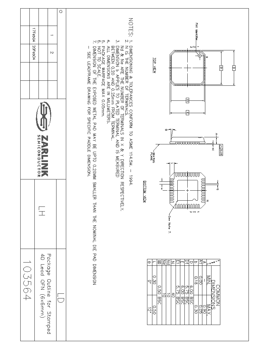
Previous package codes
Package Code
ACN
DATE
ISSUE
APPRD.
c Zarlink Semiconductor 2004 All rights reserved.

www.zarlink.com
Information relating to products and services furnished herein by Zarlink Semiconductor Inc. or its subsidiaries (collectively "Zarlink") is believed to be reliable.
However, Zarlink assumes no liability for errors that may appear in this publication, or for liability otherwise arising from the application or use of any such
information, product or service or for any infringement of patents or other intellectual property rights owned by third parties which may result from such application or
use. Neither the supply of such information or purchase of product or service conveys any license, either express or implied, under patents or other intellectual
property rights owned by Zarlink or licensed from third parties by Zarlink, whatsoever. Purchasers of products are also hereby notified that the use of product in
certain ways or in combination with Zarlink, or non-Zarlink furnished goods or services may infringe patents or other intellectual property rights owned by Zarlink.
This publication is issued to provide information only and (unless agreed by Zarlink in writing) may not be used, applied or reproduced for any purpose nor form part
of any order or contract nor to be regarded as a representation relating to the products or services concerned. The products, their specifications, services and other
information appearing in this publication are subject to change by Zarlink without notice. No warranty or guarantee express or implied is made regarding the
capability, performance or suitability of any product or service. Information concerning possible methods of use is provided as a guide only and does not constitute
any guarantee that such methods of use will be satisfactory in a specific piece of equipment. It is the user's responsibility to fully determine the performance and
suitability of any equipment using such information and to ensure that any publication or data used is up to date and has not been superseded. Manufacturing does
not necessarily include testing of all functions or parameters. These products are not suitable for use in any medical products whose failure to perform may result in
significant injury or death to the user. All products and materials are sold and services provided subject to Zarlink's conditions of sale which are available on request.
Purchase of Zarlink's I
2
C components conveys a licence under the Philips I
2
C Patent rights to use these components in and I
2
C System, provided that the system
conforms to the I
2
C Standard Specification as defined by Philips.
Zarlink, ZL and the Zarlink Semiconductor logo are trademarks of Zarlink Semiconductor Inc.
Copyright Zarlink Semiconductor Inc. All Rights Reserved.
TECHNICAL DOCUMENTATION - NOT FOR RESALE
For more information about all Zarlink products
visit our Web Site at