Document Outline
- Features
- Applications
- Description
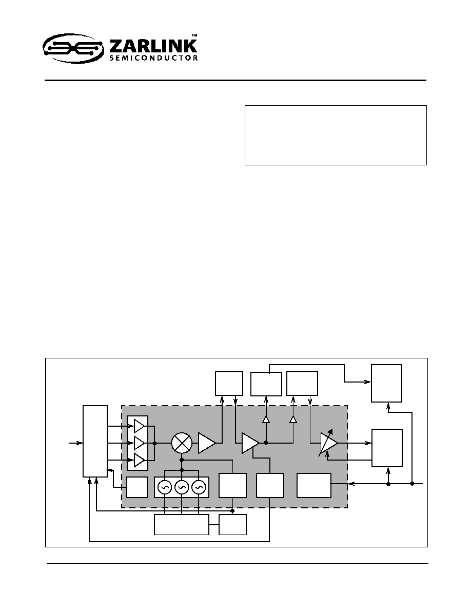
- Figure 1 - Basic Block Diagram
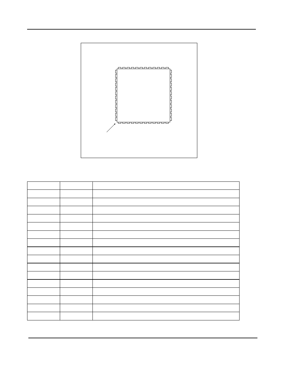
- Figure 2 - Pin Diagram
- Pin No.
- Port Name
- Function
- Table 1 - Pin Names (continued)
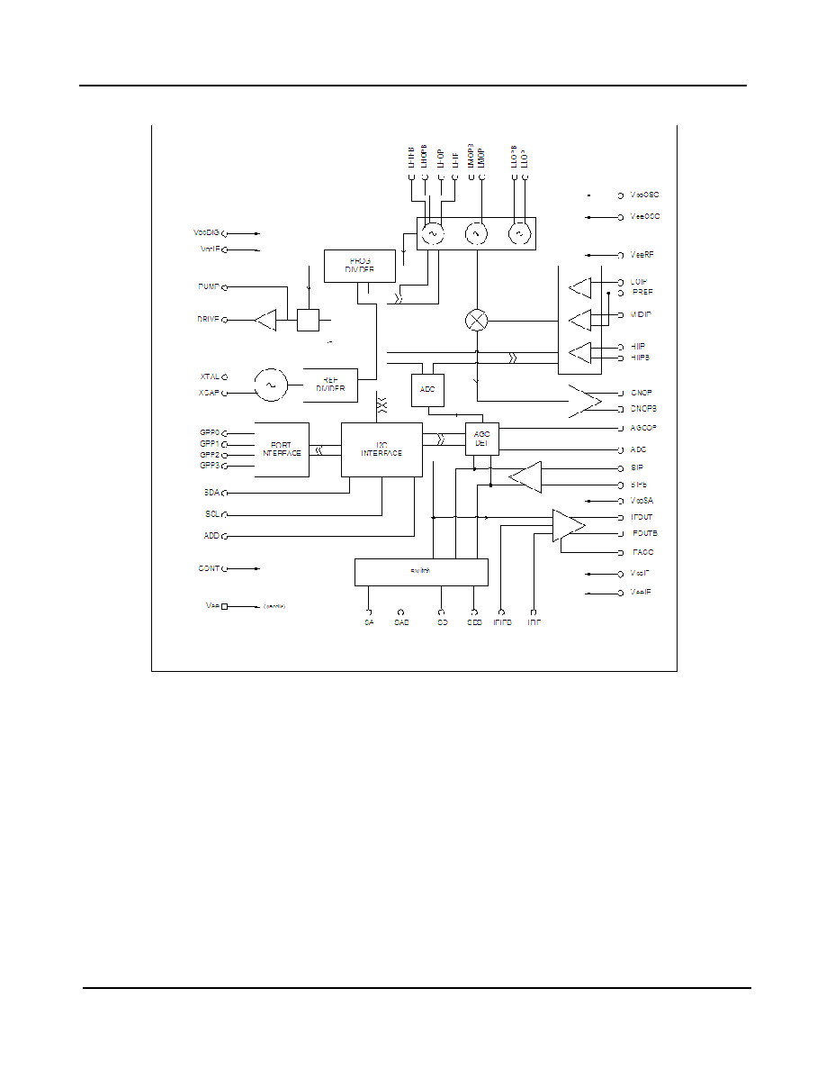
- Figure 3 - Detailed Block Diagram
- 1.0 Functional Description
- 1.1 RF Converter
- 1.2 SAW Driver Amplifier
- 1.3 AGC Detector and ADC
- 1.4 IF AGC Amplifier
- 1.5 VCO
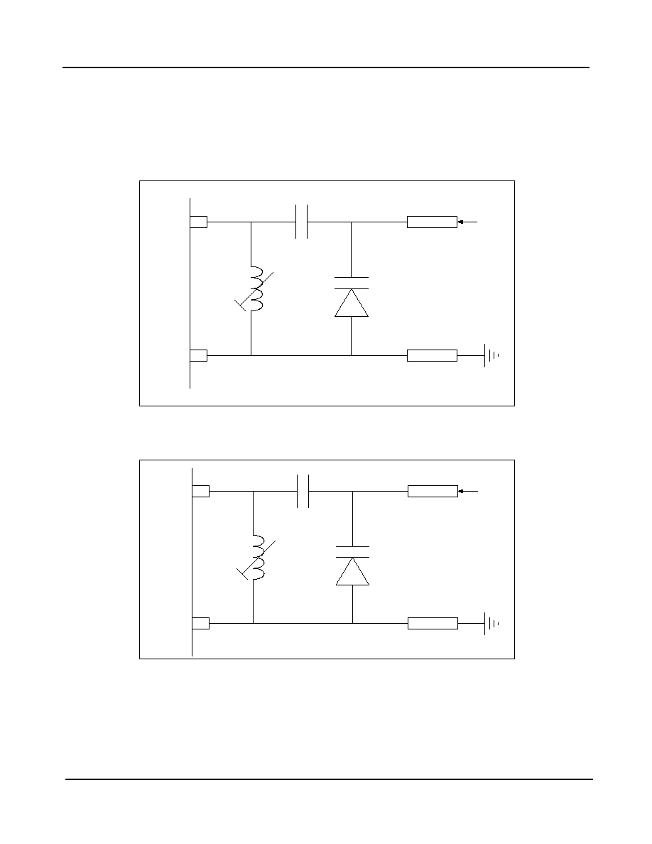
- Figure 4 - Low Band (VHF1) External Tank Circuit
- Figure 5 - Mid Band (VHF3) External Tank Circuit
- Figure 6 - High Band (UHF) External Tank Circuit
- 1.6 PLL Frequency Synthesizer
- 1.7 General Purpose Switching Ports
- 1.8 I2C Interface
- 2.0 Programming
- 2.1 Programmable Features
- Table 2 - Programmable Features
- Table 3 - Control Registers
- Table 4 - Address Bit MA1 and MA0 Settings
- Table 5 - Byte 2- LO Divider (MSB)
- Table 6 - Byte 3 LO Divider (LSB)
- Table 7 - Byte 4 PLL Control
- Table 8 - Charge Pump Current Selection
- Table 9 - Reference Divide Ratio Settings
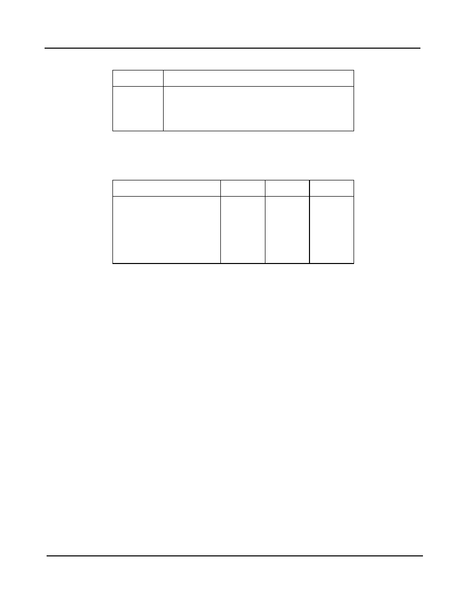
- 2.5 Control Register - Byte 5
- Table 10 - Byte 5 Control
- Table 11 - Band Selection
- SL1
- SL0
- I2C interface and registers
- Crystal oscillator
- PLL & VCO
- Converter and IF stages
- Table 12 - Internal Circuit Block Control
- Table 13 - GPPO Output Port Control
- 2.6 Control Register - Byte 6
- Table 14 - Byte 6 Control
- Table 15 - AGC Decay Current Setting
- AT2
- AT1
- AT0
- AGC Threshold (peak signal in dBmV into detector)
- Table 16 - AGC Threshold Selection
- 2.7 Control Register - Byte 7
- Bit Field
- Name
- Default
- Description
- Table 17 - Byte 7 Control
- ADS
- ADC Function
- Table 18 - ADC Input Selection
- T3
- T2
- T1
- T0
- Test Mode Description
- Table 19 - Test Modes (continued)
- 2.8 Read Mode
- Table 20 - Read Data Format (MSB is transmitted first)
- Table 21 - AGC Activity Flag Settings
- Table 22 - ADC Output Values
- 3.0 Applications Information
- Figure 7 - Typical Application Circuit (DVB-T)
- Figure 8 - Crystal Oscillator Circuit (4 MHz)
- Figure 9 - Interstage Filter
- Figure 10 - Noise Figure Measurement Conditions
- Table 23 - Optimum CP and LO Trim Settings
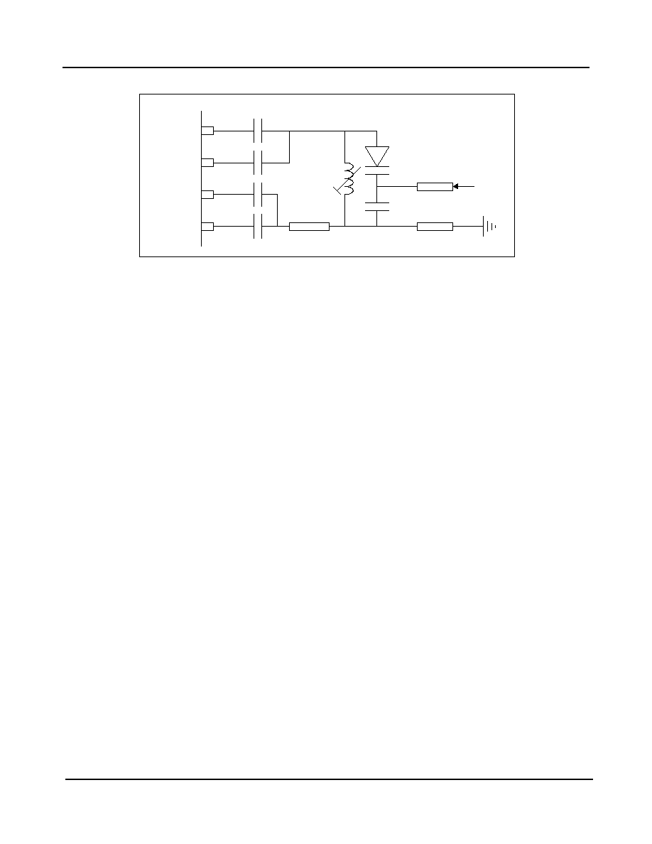
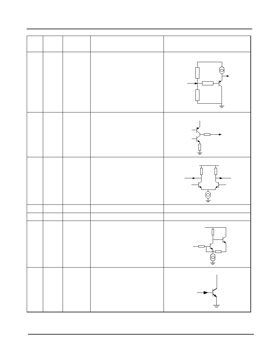
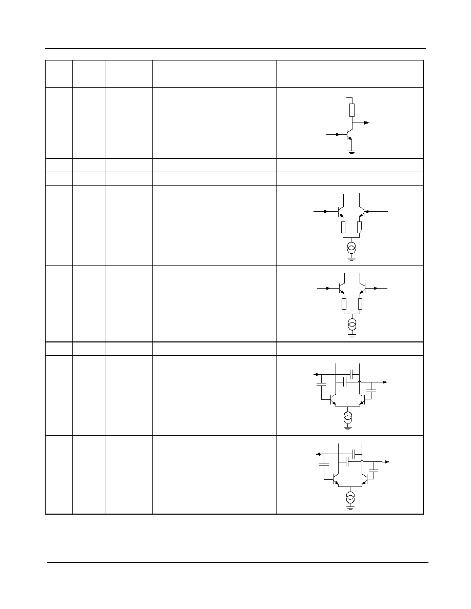
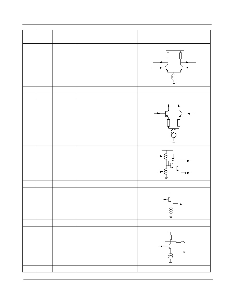
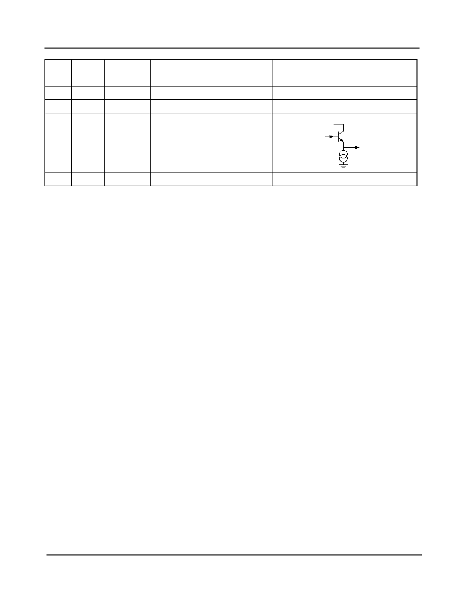
- 4.0 PIn Circuit Information
- 5.0 Absolute Maximum Ratings
- Characteristic
- Min.
- Max.
- Units
- Conditions
- 6.0 Operating Range
- Characteristic
- Min.
- Max.
- Units.
- Conditions
- 7.0 Electrical Characteristics
1
Zarlink Semiconductor Inc.
Zarlink, ZL and the Zarlink Semiconductor logo are trademarks of Zarlink Semiconductor Inc.
Copyright 2005, Zarlink Semiconductor Inc. All Rights Reserved.
Features
� Highly integrated mixer/oscillator PLL and IF AGC
amplifier for multi band analog/digital terrestrial
tuners and/or cable tuners
� Low phase noise PLL frequency synthesizer
� AGC output level detect with digital controlled
TOP threshold
� >50 dB Desired/Undesired ratio without pre
filtering
� Separate analog and digital IF outputs
� >41 dB IF AGC Control range
� Power down modes to support power reduction
initiatives
� Four independent GPO
� 48 pin QFN Package
Applications
� DVB-T receiver systems
� ISDB-T receiver systems
� DVB-C cable receiver systems
� Terrestrial analog receivers
Description
The ZL10060 is a 3 band MOPLL with IF AGC
amplifier. It down-converts the RF channel to a
standard IF followed by filtering and IF AGC
amplification for the digital channel. Each band
consists of a low noise preamplifier/mixer and local
oscillator with an external varactor tuned tank circuit.
An IF level detector is included for control of the RF
AGC. The Take Over Point and time constant are both
programmable.
The ZL10060 has high signal level handling
performance providing excellent performance in the
presence of high level unwanted signals.
All chip control is via I
2
C bus.
If higher performance is required, an alternative part,
ZL10063 is available with image reject down
conversion.
November 2005
Ordering Information
ZL10060LDG1
48 Pin QFN* Trays
ZL10060LDF1
48 Pin QFN* Tape and Reel
*Pb Free Matte Tin
-20
�
C to +85
�
C
ZL10060
MOPLL with IF AGC Amplifier
Data Sheet
Figure 1 - Basic Block Diagram
PLL
AGC
Det
I
2
C
Control
Loop
Filter
VCO Tank
Circuits
Band
Pass
Filter
Digital
Digital
LNA and T
r
ack
i
ng
Filters
ZL10060
RF
Input
Demod
Analog
Demod
GPO
IF SAW
Analog
IF SAW
I
2
C
IF AGC
Digital IF
Analog IF
RF AGC
Tuning

ZL10060
Data Sheet
Table of Contents
2
Zarlink Semiconductor Inc.
Features . . . . . . . . . . . . . . . . . . . . . . . . . . . . . . . . . . . . . . . . . . . . . . . . . . . . . . . . . . . . . . . . . . . . . . . . . . . . . . . . . 1
Applications . . . . . . . . . . . . . . . . . . . . . . . . . . . . . . . . . . . . . . . . . . . . . . . . . . . . . . . . . . . . . . . . . . . . . . . . . . . . . 1
Description . . . . . . . . . . . . . . . . . . . . . . . . . . . . . . . . . . . . . . . . . . . . . . . . . . . . . . . . . . . . . . . . . . . . . . . . . . . . . . 1
1.0 Functional Description . . . . . . . . . . . . . . . . . . . . . . . . . . . . . . . . . . . . . . . . . . . . . . . . . . . . . . . . . . . . . . . . . . 7
1.1 RF Converter . . . . . . . . . . . . . . . . . . . . . . . . . . . . . . . . . . . . . . . . . . . . . . . . . . . . . . . . . . . . . . . . . . . . . . . . 8
1.2 SAW Driver Amplifier. . . . . . . . . . . . . . . . . . . . . . . . . . . . . . . . . . . . . . . . . . . . . . . . . . . . . . . . . . . . . . . . . . 8
1.3 AGC Detector and ADC. . . . . . . . . . . . . . . . . . . . . . . . . . . . . . . . . . . . . . . . . . . . . . . . . . . . . . . . . . . . . . . . 8
1.4 IF AGC Amplifier . . . . . . . . . . . . . . . . . . . . . . . . . . . . . . . . . . . . . . . . . . . . . . . . . . . . . . . . . . . . . . . . . . . . . 8
1.5 VCO. . . . . . . . . . . . . . . . . . . . . . . . . . . . . . . . . . . . . . . . . . . . . . . . . . . . . . . . . . . . . . . . . . . . . . . . . . . . . . . 9
1.6 PLL Frequency Synthesizer . . . . . . . . . . . . . . . . . . . . . . . . . . . . . . . . . . . . . . . . . . . . . . . . . . . . . . . . . . . 10
1.7 General Purpose Switching Ports . . . . . . . . . . . . . . . . . . . . . . . . . . . . . . . . . . . . . . . . . . . . . . . . . . . . . . . 10
1.8 I
2
C Interface . . . . . . . . . . . . . . . . . . . . . . . . . . . . . . . . . . . . . . . . . . . . . . . . . . . . . . . . . . . . . . . . . . . . . . . 10
2.0 Programming . . . . . . . . . . . . . . . . . . . . . . . . . . . . . . . . . . . . . . . . . . . . . . . . . . . . . . . . . . . . . . . . . . . . . . . . . 11
2.1 Programmable Features . . . . . . . . . . . . . . . . . . . . . . . . . . . . . . . . . . . . . . . . . . . . . . . . . . . . . . . . . . . . . . 11
2.2 Register Map . . . . . . . . . . . . . . . . . . . . . . . . . . . . . . . . . . . . . . . . . . . . . . . . . . . . . . . . . . . . . . . . . . . . . . . 11
2.3 Address Register . . . . . . . . . . . . . . . . . . . . . . . . . . . . . . . . . . . . . . . . . . . . . . . . . . . . . . . . . . . . . . . . . . . . 13
2.4 PLL Registers . . . . . . . . . . . . . . . . . . . . . . . . . . . . . . . . . . . . . . . . . . . . . . . . . . . . . . . . . . . . . . . . . . . . . . 13
2.5 Control Register - Byte 5 . . . . . . . . . . . . . . . . . . . . . . . . . . . . . . . . . . . . . . . . . . . . . . . . . . . . . . . . . . . . . . 15
2.6 Control Register - Byte 6 . . . . . . . . . . . . . . . . . . . . . . . . . . . . . . . . . . . . . . . . . . . . . . . . . . . . . . . . . . . . . . 16
2.7 Control Register - Byte 7 . . . . . . . . . . . . . . . . . . . . . . . . . . . . . . . . . . . . . . . . . . . . . . . . . . . . . . . . . . . . . . 17
2.8 Read Mode . . . . . . . . . . . . . . . . . . . . . . . . . . . . . . . . . . . . . . . . . . . . . . . . . . . . . . . . . . . . . . . . . . . . . . . . 18
3.0 Applications Information. . . . . . . . . . . . . . . . . . . . . . . . . . . . . . . . . . . . . . . . . . . . . . . . . . . . . . . . . . . . . . . . 20
4.0 PIn Circuit Information . . . . . . . . . . . . . . . . . . . . . . . . . . . . . . . . . . . . . . . . . . . . . . . . . . . . . . . . . . . . . . . . . 24
5.0 Absolute Maximum Ratings . . . . . . . . . . . . . . . . . . . . . . . . . . . . . . . . . . . . . . . . . . . . . . . . . . . . . . . . . . . . . 29
6.0 Operating Range . . . . . . . . . . . . . . . . . . . . . . . . . . . . . . . . . . . . . . . . . . . . . . . . . . . . . . . . . . . . . . . . . . . . . . 29
7.0 Electrical Characteristics . . . . . . . . . . . . . . . . . . . . . . . . . . . . . . . . . . . . . . . . . . . . . . . . . . . . . . . . . . . . . . . 30

ZL10060
Data Sheet
List of Figures
3
Zarlink Semiconductor Inc.
Figure 1 - Basic Block Diagram . . . . . . . . . . . . . . . . . . . . . . . . . . . . . . . . . . . . . . . . . . . . . . . . . . . . . . . . . . . . . . . . 1
Figure 2 - Pin Diagram. . . . . . . . . . . . . . . . . . . . . . . . . . . . . . . . . . . . . . . . . . . . . . . . . . . . . . . . . . . . . . . . . . . . . . . 5
Figure 3 - Detailed Block Diagram . . . . . . . . . . . . . . . . . . . . . . . . . . . . . . . . . . . . . . . . . . . . . . . . . . . . . . . . . . . . . . 7
Figure 4 - Low Band (VHF1) External Tank Circuit . . . . . . . . . . . . . . . . . . . . . . . . . . . . . . . . . . . . . . . . . . . . . . . . . 9
Figure 5 - Mid Band (VHF3) External Tank Circuit. . . . . . . . . . . . . . . . . . . . . . . . . . . . . . . . . . . . . . . . . . . . . . . . . . 9
Figure 6 - High Band (UHF) External Tank Circuit . . . . . . . . . . . . . . . . . . . . . . . . . . . . . . . . . . . . . . . . . . . . . . . . . 10
Figure 7 - Typical Application Circuit (DVB-T) . . . . . . . . . . . . . . . . . . . . . . . . . . . . . . . . . . . . . . . . . . . . . . . . . . . . 20
Figure 8 - Crystal Oscillator Circuit (4 MHz). . . . . . . . . . . . . . . . . . . . . . . . . . . . . . . . . . . . . . . . . . . . . . . . . . . . . . 21
Figure 9 - Interstage Filter . . . . . . . . . . . . . . . . . . . . . . . . . . . . . . . . . . . . . . . . . . . . . . . . . . . . . . . . . . . . . . . . . . . 22
Figure 10 - Noise Figure Measurement Conditions . . . . . . . . . . . . . . . . . . . . . . . . . . . . . . . . . . . . . . . . . . . . . . . . 23

ZL10060
Data Sheet
List of Tables
4
Zarlink Semiconductor Inc.
Table 1 - Pin Names. . . . . . . . . . . . . . . . . . . . . . . . . . . . . . . . . . . . . . . . . . . . . . . . . . . . . . . . . . . . . . . . . . . . . . . . . 5
Table 2 - Programmable Features . . . . . . . . . . . . . . . . . . . . . . . . . . . . . . . . . . . . . . . . . . . . . . . . . . . . . . . . . . . . . 11
Table 3 - Control Registers . . . . . . . . . . . . . . . . . . . . . . . . . . . . . . . . . . . . . . . . . . . . . . . . . . . . . . . . . . . . . . . . . . 12
Table 4 - Address Bit MA1 and MA0 Settings . . . . . . . . . . . . . . . . . . . . . . . . . . . . . . . . . . . . . . . . . . . . . . . . . . . . 13
Table 5 - Byte 2- LO Divider (MSB) . . . . . . . . . . . . . . . . . . . . . . . . . . . . . . . . . . . . . . . . . . . . . . . . . . . . . . . . . . . . 13
Table 6 - Byte 3 LO Divider (LSB) . . . . . . . . . . . . . . . . . . . . . . . . . . . . . . . . . . . . . . . . . . . . . . . . . . . . . . . . . . . . . 13
Table 7 - Byte 4 PLL Control . . . . . . . . . . . . . . . . . . . . . . . . . . . . . . . . . . . . . . . . . . . . . . . . . . . . . . . . . . . . . . . . . 13
Table 8 - Charge Pump Current Selection . . . . . . . . . . . . . . . . . . . . . . . . . . . . . . . . . . . . . . . . . . . . . . . . . . . . . . . 13
Table 9 - Reference Divide Ratio Settings . . . . . . . . . . . . . . . . . . . . . . . . . . . . . . . . . . . . . . . . . . . . . . . . . . . . . . . 14
Table 10 - Byte 5 Control . . . . . . . . . . . . . . . . . . . . . . . . . . . . . . . . . . . . . . . . . . . . . . . . . . . . . . . . . . . . . . . . . . . . 15
Table 11 - Band Selection . . . . . . . . . . . . . . . . . . . . . . . . . . . . . . . . . . . . . . . . . . . . . . . . . . . . . . . . . . . . . . . . . . . 15
Table 12 - Internal Circuit Block Control. . . . . . . . . . . . . . . . . . . . . . . . . . . . . . . . . . . . . . . . . . . . . . . . . . . . . . . . . 15
Table 13 - GPPO Output Port Control . . . . . . . . . . . . . . . . . . . . . . . . . . . . . . . . . . . . . . . . . . . . . . . . . . . . . . . . . . 15
Table 14 - Byte 6 Control . . . . . . . . . . . . . . . . . . . . . . . . . . . . . . . . . . . . . . . . . . . . . . . . . . . . . . . . . . . . . . . . . . . . 16
Table 15 - AGC Decay Current Setting . . . . . . . . . . . . . . . . . . . . . . . . . . . . . . . . . . . . . . . . . . . . . . . . . . . . . . . . . 16
Table 16 - AGC Threshold Selection . . . . . . . . . . . . . . . . . . . . . . . . . . . . . . . . . . . . . . . . . . . . . . . . . . . . . . . . . . . 17
Table 17 - Byte 7 Control . . . . . . . . . . . . . . . . . . . . . . . . . . . . . . . . . . . . . . . . . . . . . . . . . . . . . . . . . . . . . . . . . . . . 17
Table 18 - ADC Input Selection . . . . . . . . . . . . . . . . . . . . . . . . . . . . . . . . . . . . . . . . . . . . . . . . . . . . . . . . . . . . . . . 17
Table 19 - Test Modes . . . . . . . . . . . . . . . . . . . . . . . . . . . . . . . . . . . . . . . . . . . . . . . . . . . . . . . . . . . . . . . . . . . . . . 17
Table 20 - Read Data Format (MSB is transmitted first) . . . . . . . . . . . . . . . . . . . . . . . . . . . . . . . . . . . . . . . . . . . . 18
Table 21 - AGC Activity Flag Settings . . . . . . . . . . . . . . . . . . . . . . . . . . . . . . . . . . . . . . . . . . . . . . . . . . . . . . . . . . 19
Table 22 - ADC Output Values . . . . . . . . . . . . . . . . . . . . . . . . . . . . . . . . . . . . . . . . . . . . . . . . . . . . . . . . . . . . . . . . 19
Table 23 - Optimum CP and LO Trim Settings. . . . . . . . . . . . . . . . . . . . . . . . . . . . . . . . . . . . . . . . . . . . . . . . . . . . 23
ZL10060
Data Sheet
5
Zarlink Semiconductor Inc.
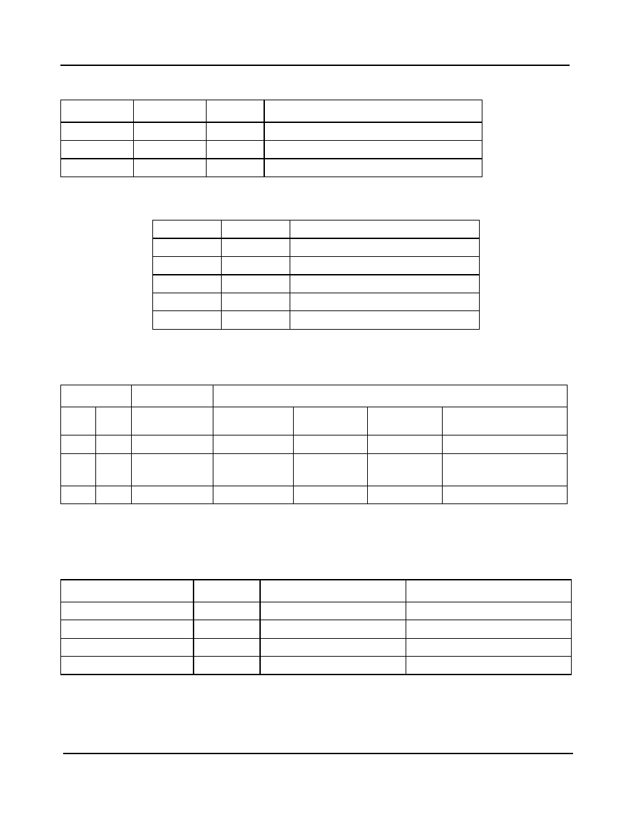
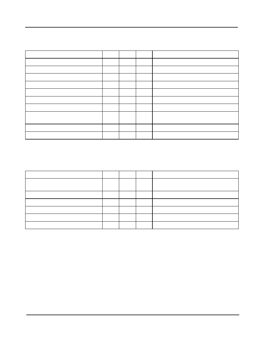
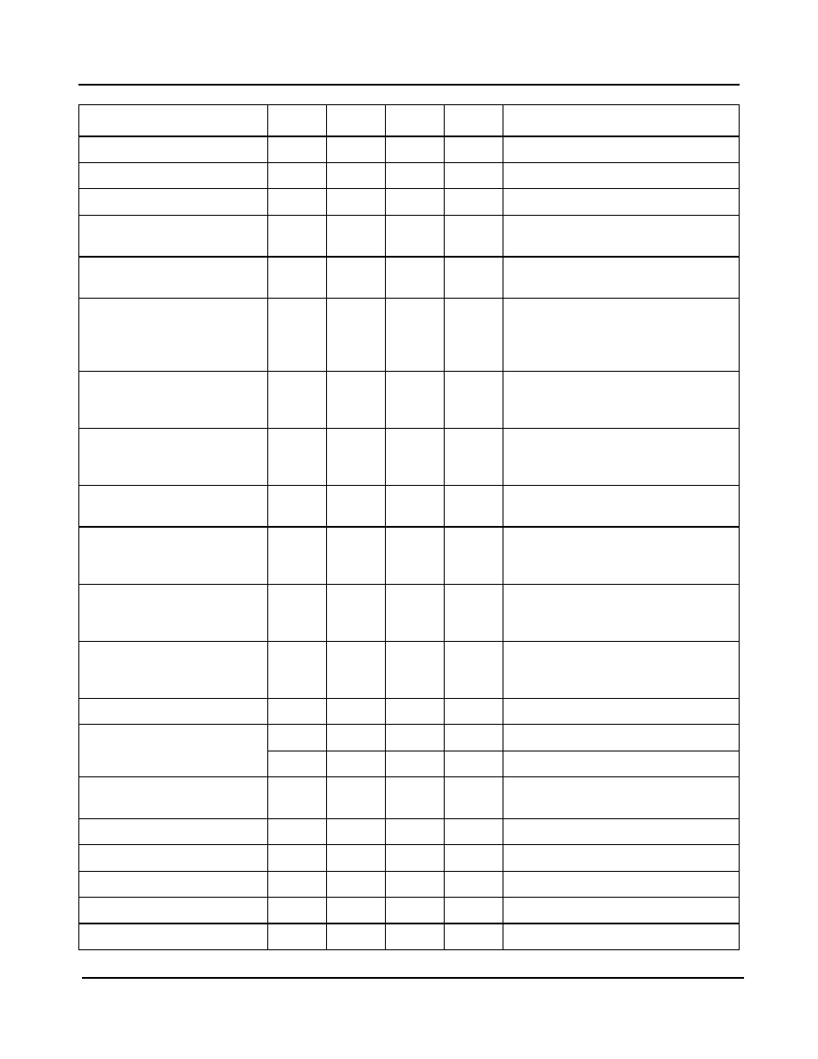
Figure 2 - Pin Diagram
Pin No.
Port Name
Function
1
IFAGC
IF amplifier AGC input
2
SAB
SAW filter driver output (analog)
3
SA
SAW filter driver output (analog)
4
ADC
External ADC input
5
SDA
I
2
C bus serial data input/output
6
SCL
I
2
C bus serial clock input
7
ADD I
2
C bus address selection input
8
AGCOP AGC
output
9
CNOPB
Analog converter output
10
CNOP
Analog converter output
11
CONT Paddle
(Ground)
12
VccRF
RF section supply
13
SIPB
SAW filter driver input
14
SIP
SAW filter driver input
15
GPP0
General purpose switching port
16
GPP1
General purpose switching port
Table 1 - Pin Names
AGCOP
ZL10060
CNOP
CNOPB
ADC
SCL
SDA
LHOPB
LHIPB
VeeOSC
LMOPB
LHOP
LHIP
LMOP
Ve
e
R
F
GPP2
IP
R
E
F
GPP0 G
PP1
SI
PB
SI
P
LOI
P
SA
IFAGC
SAB
VccOSC
IFIP
IFIPB
Vee
I
F
IF
O
P
B
IF
O
P
XT
A
L
Vc
c
I
F
SD
B
Vc
c
I
F
SD
PU
M
P
Vc
c
D
I
G
1
VccRF
CONT
LLOPB
LLOP
HI
IP
B
GPP3
XC
AP
DR
IV
E
HI
IP
MI
D
I
P
ADD
Vee
(PACKAGE
PADDLE)

ZL10060
Data Sheet
6
Zarlink Semiconductor Inc.
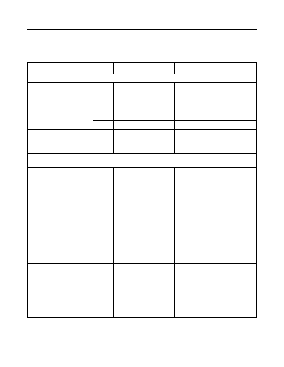
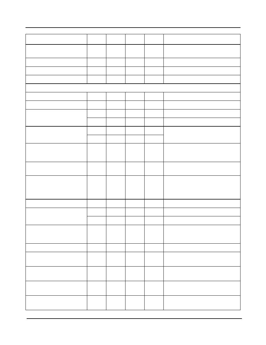
17
GPP2
General purpose switching port
18
VeeRF RF
section
ground
19
LOIP
Low band input
20
IPREF
Reference input for low and mid bands
21
MIDIP
Mid band input
22
HIIP High
band
input
23
HIIPB
High band inverse input
24
GPP3
General purpose switching port
25
LLOP
Low band local oscillator output
26
LLOPB
Low band local oscillator inverse output
27
LMOP
Mid band local oscillator output
28
LMOPB
Mid band local oscillator inverse output
29
LHIP
High band local oscillator input
30
LHOP
High band local oscillator output
31
LHOPB
High band local oscillator inverse output
32
LHIPB
High band local oscillator inverse input
33
VeeOSC Oscillator
section
ground
34
VccOSC
Oscillator supply
35
IFIP
IF amplifier input
36
IFIPB
IF amplifier inverse input
37
DRIVE
Loop amplifier drive output
38
PUMP
Loop amplifier charge pump output
39
VccDIG
Digital section supply
40
SD
SAW filter driver output (digital)
41
SDB
SAW filter driver output (digital)
42
VccIF
IF amplifier section supply
43
XCAP Reference
oscillator feedback input
44
XTAL
Reference oscillator crystal drive
45
VccIF
IF amplifier section supply
46
VeeIF
IF section ground
47
IFOP
IF amplifier output
48
IFOPB
IF amplifier inverse output
Paddle
Vee
Global ground
Pin No.
Port Name
Function
Table 1 - Pin Names (continued)
ZL10060
Data Sheet
7
Zarlink Semiconductor Inc.
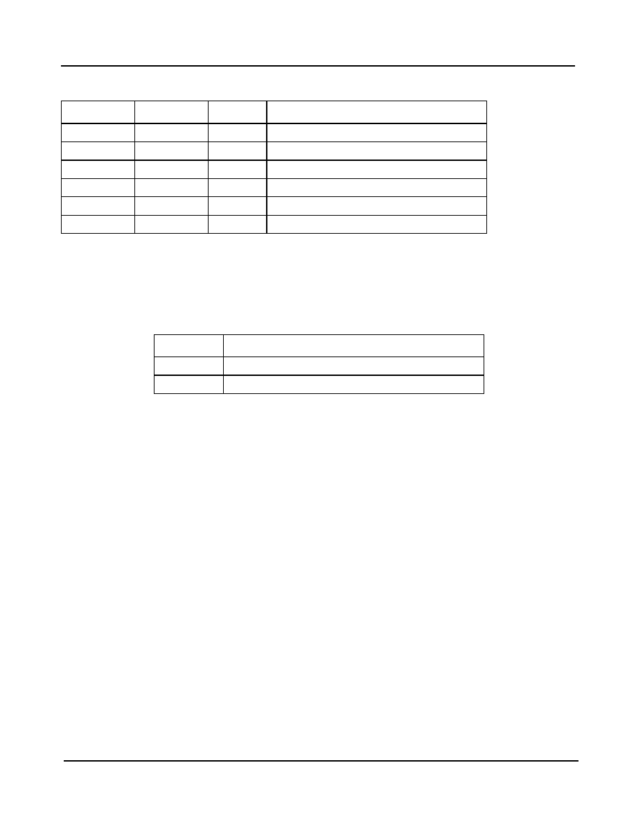
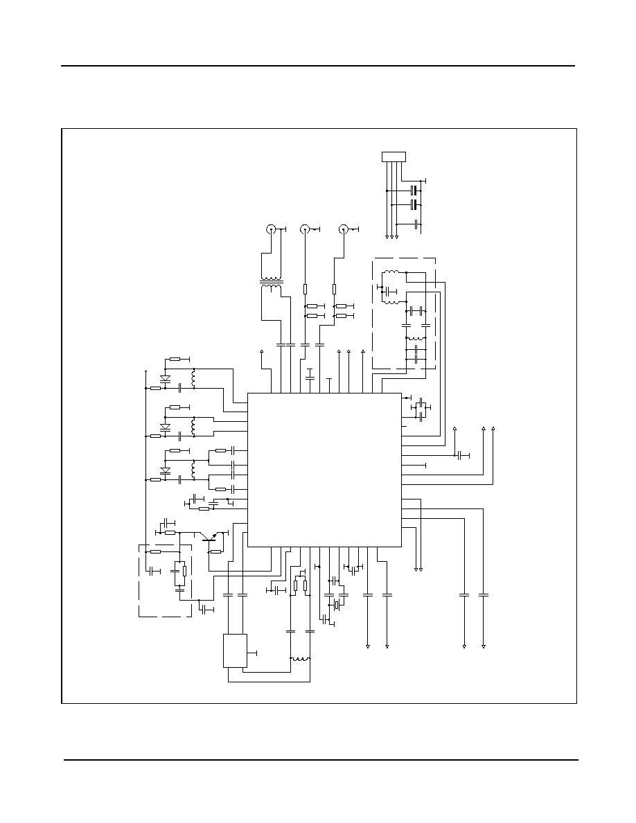
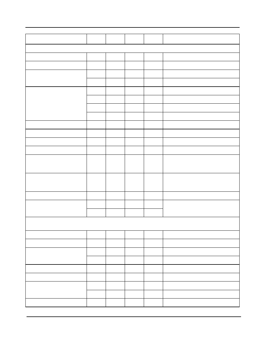
Figure 3 - Detailed Block Diagram
1.0 Functional Description
The ZL10060 is a three-band RF mixer oscillator with on-board frequency synthesizer and IF AGC amplifier,
integrating all tuner active circuitry after the tracking filter in a single package.
It is intended for use in all band terrestrial tuners, and requires a minimum external component count. It contains all
elements required for RF down conversion to a standard IF with the exception of external VCO tank circuits.
In normal application the RF input is interfaced to the selected mixer oscillator preamplifier through the tuner pre-
filter and AGC stages. The ZL10060 provides an RF AGC control signal, which can be used to control the RF gain.
The preamplifier output feeds the mixer stage where the required channel is down converted to the IF frequency.
The local oscillator frequency for the down conversion is obtained from the on board PLL and local oscillator, with
an external varactor tuned tank.
The downconverted signal is then passed through an external filter into a SAW filter driver amplifier. This provides
two output channels for hybrid analog and digital applications.

ZL10060
Data Sheet
8
Zarlink Semiconductor Inc.
An AGC IF amplifier is included which provides an output signal to a digital demodulator.
The device is controlled through an I
2
C compatible interface.
1.1 RF Converter
The ZL10060 contains three input stages to cover the VHF1, VHF3 and UHF frequency bands. The inputs would
normally be driven by front end amplifiers and tracking filters. All three inputs are differential, however, the VHF1
and VHF3 inputs would normally be single ended. These inputs therefore can share a common input reference pin.
The UHF input should be driven with a differential signal. The inputs are all high impedance. The differential
converter IF output is then passed through an external interstage filter. This can be tuned for 36 MHz for DVB-T
applications but can also be used at 44 MHz and 57 MHz to be compatible with other TV standards. The
recommended filter circuit is shown in Figure 9. The design of this filter provides an impedance transformation as
well as rejection of adjacent channels. A 0.5 dB Chebychev filter with 10 MHz bandwidth is recommended. This
gives a flat response across the pass band and takes into account normal component tolerances.
1.2 SAW Driver Amplifier
The output of the interstage filter then passes to the SAW filter drive amplifier. This provides further amplification
and interfaces to the SAW filter. Two SAW filter drive outputs are provided for hybrid analog and digital applications.
Both output stages are identical however the digital output (SD, SDB) should always be used for digital applications
as the pin out of the device has been optimized to give the best isolation performance in this configuration. Output
selection is programmable however it should be noted that the unselected output is not powered off but operates at
a lower power level which means that a signal will still be present on the output.
The differential outputs will drive a balanced SAW filter with a tuning inductor to resonate with the SAW filter input
capacitance. The SAW filter can also be driven without the tuning inductor but with the addition of 350 ohm resistors
to ground on the SAW driver outputs to increase the output drive capability. This will increase total current
consumption by 14 mA.
1.3 AGC Detector and ADC
The ZL10060 contains a broadband AGC detector circuit which provides an output to provide gain control for the
RF frontend gain stages. The detector input signal is derived from the signal level in the SAW driver amplifier. The
composite signal at this point is the wanted signal plus adjacent channels (N +/- 1, N +/- 2, N +/- 3). The AGC
detector threshold point at which the agc output becomes active can be programmed to one of eight levels via the
I
2
C interface. When the composite level reaches the agc threshold, the agc output pin will be active. The AGC
attack current is fixed, however, the decay current can be programmed to two levels. The agc output can only drive
a high impedance e.g., a dual gate FET. If RF gain control uses a PiN diode then a simple buffer circuit will be
required.
An AGC flag output is also available through the I
2
C interface. This indicates when the AGC output is active i.e.,
less than 4 volts.
The agc output level can also be monitored by an on chip 3 bit ADC. Although the ADC is 3 bits, only 5 levels are
available. Alternatively the ADC can be programmed to measure the voltage on an external pin (ADC Pin 4).
1.4 IF AGC Amplifier
The AGC amplifier amplifies the output of the SAW filter for the digital channel and provides a differential output to
the demodulator. The analog gain control signal is normally derived from the demodulator. At least 41 dB of gain
control is provided.
The AGC amplifier can be powered down independently of the rest of the device if not required. This mode could be
used in analog applications to reduce overall power consumption.
ZL10060
Data Sheet
9
Zarlink Semiconductor Inc.
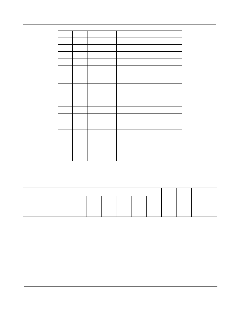
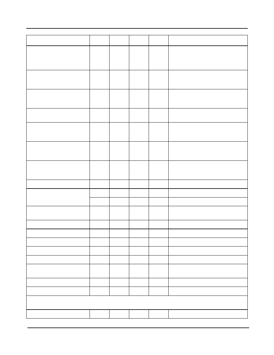
1.5 VCO
Separate VCO's are provided for each band. The oscillator circuits are on chip however the tank circuitry is
external. All three oscillators are differential. The typical external tank circuits are shown in Figures 4, 5 and 6. It is
essential to take care to minimize track lengths and parasitics when designing the PCB layout to obtain best
performance. The close-in phase noise of the local oscillator can be optimized at the programmed operating
frequency by a programming bit which increases bias current in the VCO.
.
Figure 4 - Low Band (VHF1) External Tank Circuit
Figure 5 - Mid Band (VHF3) External Tank Circuit
LLOPB
LLOP
Vvar
R_bias
R_bias
Cs pF
L1 nH
LMOPB
LMOP
Vvar
R_bias
R_bias
Cs pF
L1 nH
ZL10060
Data Sheet
10
Zarlink Semiconductor Inc.
Figure 6 - High Band (UHF) External Tank Circuit
1.6 PLL Frequency Synthesizer
The PLL frequency synthesizer section contains all the elements necessary, with the exception of a frequency
reference and loop filter to control a varicap tuned local oscillator, to form a complete PLL frequency synthesized
source. The device allows for operation with a high comparison frequency and is fabricated in high speed logic,
which enables the generation of a loop with good phase noise performance. It can be operated with comparison
frequencies appropriate for frequency offsets as required in digital terrestrial (DTT) receivers.
The LO input signal from the selected oscillator section is routed to an internal preamplifier, which provides gain
and reverse isolation from the divider signals. The output of the preamplifier interfaces directly to the 15-bit
programmable divider, which is of MN+A architecture, with a 16/17 dual modulus prescaler. The A counter is 4-bits,
and the M counter is 11 bits.
The output of the programmable divider is fed to the phase comparator where it is compared in both phase and
frequency domain with the comparison frequency which is derived either from the on-board crystal controlled
oscillator, or from an external reference source. In both cases the reference frequency is divided down to the
comparison frequency by the reference divider, which is programmable into 1 of 16 ratios.
The output of the phase detector feeds a charge pump and loop amplifier section, which when used with an
external loop filter, integrates the current pulses into the varactor control voltage.
The programmable divider output, F
pd
, divided by two and the reference divider output, F
comp
, can be switched to
port P0 by programming the device into a test mode.
The PLL includes a lock detect circuit. The lock detect output is available by reading the Status byte on the I
2
C
interface
1.7 General Purpose Switching Ports
The ZL10060 has four output switching ports. Three of these ports (GPP[3:1]) incorporate a 10 kohm pull up
resistor. The remaining port (GPP0) is an open collector switch. These ports can be used for switching external RF
input stages for example. Ports GPP[1:0] can also be used as test outputs for debug purposes.
1.8 I
2
C Interface
The ZL10060 is controlled by an I
2
C data bus and is compatible with both 3.3 V and 5 V control levels.
Data and Clock are fed in on the SDA and SCL lines respectively as defined by I
2
C bus format. The device can
either accept data (write mode), or send data (read mode). The LSB of the address byte (R/W) sets the device into
write mode if it is low, and read mode if it is high. The device can be programmed to respond to 1 of 4 addresses,
LHIPB
LHOPB
LHOP
LHIP
Vvar
R_bias
R_bias
Cs pF
L1 nH
Cp
R_damp
Cp
Cp
Cp
ZL10060
Data Sheet
11
Zarlink Semiconductor Inc.
which enables the use of more than one device in an I
2
C bus system. The address is selected by applying a voltage
to the `ADD' input.
When the device receives a valid address byte, it pulls the SDA line low during the acknowledge period, and during
following acknowledge periods after further data bytes are received. When the device is programmed into read
mode, the controller accepting the data must pull the SDA line low during all status byte acknowledge periods to
read another status byte. If the controller fails to pull the SDA line low during this period, the device generates an
internal STOP condition, which inhibits further reading.
2.0 Programming
The ZL10060 is fully programmable through the I
2
C interface. The device can also output data to the controller.
2.1 Programmable Features
2.2 Register Map
There are a total of 7 write registers, the first of which is the Address register. The control registers are described in
detail in the following section. The MSB of each register is written first.
After reception and acknowledgement of a correct address (byte 1), the first bit of the following byte determines
whether the byte is interpreted as a byte 2 or 4, a logic '0' indicating byte 2, and a logic '1' indicating byte 4. Having
Feature
Description
RF programmable
divider
Programs PLL main divider
Reference
programmable divider
Programs PLL reference divider to set required frequency step
Band selection
Selects RF input and appropriate LO oscillator.
AGC Threshold
Sets the Input Power Level Threshold at which the AGC detector starts to generate a
control level.
AGC Decay
Sets the AGC decay current.
Charge pump current
Selects one of the four charge pump current settings.
IF amplifier function
The IF amplifier can be enabled independently of other circuit blocks.
SAWF output select
Select the analog or digital SAW driver output.
Ports GPP[3:1]
These are configured as NPN buffers with 10 kohm pull-up resistors to V
cc
.
Logic `1' = on
Logic `0' = off; default on power up
PORT GPP0
This is configured as a NPN open collector buffer. Logic `1' = on
Logic `0' = off; default on power up
VCO Trim
Adjusts the VCO bias current to provide optimum phase noise performance.
ADC input Select
Select either the internal AGC detect output level or the external level applied to the
ADC input pin.
Programmable power
The ZL10060 has various power saving modes.
Test modes
Test modes to monitor and control internal PLL signals.
Table 2 - Programmable Features
ZL10060
Data Sheet
12
Zarlink Semiconductor Inc.
interpreted this byte as either byte 2 or 4 the following data byte will be interpreted as byte 3 or 5 respectively. Byte
5 will be followed by byte 6 or a stop condition. Byte 6 will be followed by byte 7 or a stop condition. Byte 7 will be
followed by a stop condition or a byte 2 or byte 4 as described above. Further data bytes can be programmed
following the above-described protocol. A STOP condition can be generated after any data byte, if however it
occurs during a byte transmission, the previous byte data is retained. To facilitate smooth fine tuning, the frequency
data bytes are only accepted by the device after all 15 bits of frequency data have been received, or after the
generation of a STOP condition.
MSB
LSB
ACK
7
6
5
4
3
2
1
0
Address
1
1
0
0
0
MA1
MA0
0
A
Byte 1
Programmable
divider
0
D14
D13
D12
D11
D10
D9
D8
A
Byte 2W
Programmable
divider
D7
D6
D5
D4
D3
D2
D1
D0
A
Byte 3W
Control data
1
C1
C0
R4
R3
R2
R1
R0
A
Byte 4W
Control data
BS1
BS0
SL1
SL0
P3
P2
P1
P0
A
Byte 5W
Control Data
LO1
LO0
ATC
IFE
X
AT2
AT1
AT0
A
Byte 6W
Control Data
SAS
X
AGD
ADS
T3
T2
T1
T0
A
Byte 7W
Table 3 - Control Registers
A
Acknowledge bit
MA1, MA0
Address bits
D14-D0
Programmable division ratio control bits
R4-R0
Reference division ratio select
C1, C0
Charge pump current select
BS1-BS0
Band select bits
SL1-SL0
Power down modes
SAS
SAWF drive output select
P3-P0
P3-P0 port output states
ADS
ADC input select
ATC
AGC Decay Current
AGD
AGC Disable
AT2:AT0
AGC Onset threshold Control
LO1:LO0
LO trim control bits
T3-T0
Test mode control bits
IFE
IF AGC amplifier enable
X
Don't Care
ZL10060
Data Sheet
13
Zarlink Semiconductor Inc.
Details of the programming registers are shown in the following sections. Default values on power up are also
shown.
2.3 Address Register
The ZL10060 address (MA1, MA0) are determined by the voltage set at the address pin (ADD) as shown in Table 4.
2.4 PLL Registers
Bytes 2,3 and 4 are used to program the PLL.
The LO frequency will not be updated until both Byte 1 and Byte 2 have been programmed.
The charge pump current values are selected from the following table:
Address Select (Byte 1)
MA1
MA0
Address Input Voltage Level
0
0
0 - 0.1Vcc (Connect to V
ee
)
0
1
0.2V
cc
� 0.3V
cc
(Open circuit)
1
0
0.4 V
cc
� 0.6 V
cc
(30K
to V
cc
)
1
1
0.9 V
cc
- 1.0 V
cc
(Connect to V
cc
)
Table 4 - Address Bit MA1 and MA0 Settings
Bit Field
Name
Default
Description
7
-
0
Must be set to 0
6:0
D[14:8]
0
MSB bits of LO Divider register.
Table 5 - Byte 2- LO Divider (MSB)
Bit Field
Name
Default
Description
7:0
D[7:0]
0
LSB bits of LO Divider register.
Table 6 - Byte 3 LO Divider (LSB)
Bit Field
Name
Default
Description
7
-
1
Must be set to 1
6:5
C[1:0]
0
Charge pump current.
4:0
R[4:0]
10011
Reference divider control.
Table 7 - Byte 4 PLL Control
C1
C0
Current
�
A
0
0
+-155
Table 8 - Charge Pump Current Selection

ZL10060
Data Sheet
14
Zarlink Semiconductor Inc.
The reference divider ratio can be selected from the following table:
0
1
+-330
1
0
+-690
1
1
+-1450
Default State on power up = 00
R4
R3
R2
R1
R0
Ratio
0
0
0
1
1
16
0
0
1
0
0
32
0
0
1
0
1
64
0
0
1
1
0
128
0
1
0
1
1
20
0
1
1
0
0
40
0
1
1
0
1
80
0
1
1
1
0
160
1
0
0
1
1
24
1
0
1
0
0
48
1
0
1
0
1
96
1
0
1
1
0
192
1
1
0
1
1
28
1
1
1
0
0
56
1
1
1
0
1
112
1
1
1
1
0
224
Default State on power up = 10011
Table 9 - Reference Divide Ratio Settings
C1
C0
Current
�
A
Table 8 - Charge Pump Current Selection
ZL10060
Data Sheet
15
Zarlink Semiconductor Inc.
2.5 Control Register - Byte 5
The band switching is controlled as shown below:
The various power-up modes are shown below. The IF AGC amplifier is controlled separately The I
2
C interface and
crystal oscillator circuit is active in all modes
.
The ZL10060 has four output ports. Ports [3:1] have an internal 10 kohm pull up resistor to Vcc. GPP0 is open
collector.
Bit Field
Name
Default
Description
7:6
BS[1:0]
11
Band Switching
5:4
SL[1:0]
01
Power-up modes
3:0
P[3:0]
0
General Purpose Output ports
Table 10 - Byte 5 Control
BS1
BS0
Band Selected
0
0
LO Band
0
1
MID Band
1
0
HI band
1
1
All off
Default state on power up = 11
Table 11 - Band Selection
Power Mode
Section Status
SL1
SL0
I
2
C interface
and registers
Crystal
oscillator
PLL & VCO
Converter and IF
stages
0
X
Sleep
Enabled
Enabled
Disabled
Disabled
1
0
PLL and
VCO enabled
Enabled
Enabled
Enabled
Disabled
1
1
Full
Enabled
Enabled
Enabled
Enabled
Table 12 - Internal Circuit Block Control
Function
Bit
0
1
GPP0 output Enable
P0
Off (High Impedance)
On (Current Sink)
GPP1 output Enable
P1
Off
On (Current Sink)
GPP2 output Enable
P2
Off
On (Current Sink)
GPP3 output Enable
P3
Off
On (Current Sink)
Table 13 - GPPO Output Port Control
ZL10060
Data Sheet
16
Zarlink Semiconductor Inc.
2.6 Control Register - Byte 6
The VCO bias trim adjusts the VCO bias to give optimum close-in phase noise. In general this should be set to 1 for
the lower third of the VCO frequency range.
The AGC attack current is fixed at 100
�
A however the agc decay current can be programmed to one of two values
as shown below. If the PLL is unlocked (FL = 0), then the ATC control is over-ridden and the AGC decay current is
set to 10
�
A. When the PLL locks (FL = 1) the decay current reverts to the programmed ATC value.
Bit Field
Name
Default
Description
7
LO1
0
VCO Bias Trim
6
LO0
0
Not used
5
ATC
0
AGC Decay current select
4
IFE
0
IF AGC Amplifier enable (1 = On)
3
X
0
Not used
2:0
AT[2:0]
0
AGC Threshold Select
Table 14 - Byte 6 Control
ATC
AGC Decay Current (
�
A)
0
10.0
1
0.3
Table 15 - AGC Decay Current Setting

ZL10060
Data Sheet
17
Zarlink Semiconductor Inc.
The AGC threshold can be programmed using the AT[2:0] bits. Note that the programmed value is dB
�
V peak.
2.7 Control Register - Byte 7
The ADC input selection is shown in the table below
The test bits T[3:0] allow internal PLL signals to be monitored and also to manually control charge pump current
and AGC detector output. This facilities may be useful during debug. The test bit selection is shown below. The
reserved test modes should not be used.
AT2
AT1
AT0
AGC Threshold
(peak signal in dB
�
V into detector)
0
0
0
120
0
0
1
118
0
1
0
116
0
1
1
114
1
0
0
112
1
0
1
110
1
1
0
107
1
1
1
104
Default state on power up = 000
Table 16 - AGC Threshold Selection
Bit Field
Name
Default
Description
7
SAS
1
Digital SAW Drive Output Select (1 = Digital)
6
X
0
Not used
5
AGD
1
AGC Detector Enable (0 = Enabled)
4
ADS
0
ADC Input select
3:0
T[3:0]
0
Test Bits
Table 17 - Byte 7 Control
ADS
ADC Function
0
AGC Output
1
External ADC input
Table 18 - ADC Input Selection
T3
T2
T1
T0
Test Mode Description
0
0
0
0
Normal operation
0
0
0
1
Reserved Test Mode
0
0
1
0
AGC Sink, Force I
agc
= -100
�
A
0
0
1
1
AGC Source, Force I
agc
= 10
�
A
P0 = Output of AGC bias DAC
Table 19 - Test Modes
ZL10060
Data Sheet
18
Zarlink Semiconductor Inc.
2.8 Read Mode
When the device is in read mode, the status byte read from the device takes the form shown in Table 20.
The following describes data read through the read byte;
� Bit 7 (POR) is the power-on reset indicator, and this is set to a logic '1' if the V
cc
supply to the device has
dropped below 3 V (at 25
�
C), e.g., when the device is initially turned ON. The POR is reset to '0' when the
read sequence is terminated by a STOP command. When POR is set high this indicates that the
programmed information may have been corrupted and the device reset to power up condition.
� Bit 6 (FL) is the PLL lock flag and indicates whether the device is phase locked, a logic '1' is present if the
device is locked, and a logic '0' if the device is unlocked. The FL bit is set after 64 consecutive comparison
cycles in lock.
0
1
0
0
Reserved Test Mode
0
1
0
1
Reserved Test Mode
0
1
1
0
Reserved Test Mode
0
1
1
1
Reserved Test Mode
1
0
0
0
Reserved Test Mode
1
0
0
1
Charge pump sink *
Status byte FL set to logic `0'
1
0
1
0
Charge pump source *
Status byte FL set to logic `0'
1
0
1
1
Charge pump disabled *
Status byte FL set to logic `1'
1
1
0
0
Port P0 = F
pd
/2
1
1
0
1
Charge pump sink *
Status byte FL set to logic `0'
Port P0 = F
comp
1
1
1
0
Charge pump source *
Status byte FL set to logic `0'
Port P0 = F
comp
1
1
1
1
Charge pump disabled *
Status byte FL set to logic `1'
Port P0 = F
comp
MSB
LSB
ACK
7
6
5
4
3
2
1
0
Address
1
1
0
0
0
MA1
MA0
1
A
Byte 1
Status Byte
POR
FL
1
1
AGF
V2
V1
V0
A
Byte 2R
Table 20 - Read Data Format (MSB is transmitted first)
T3
T2
T1
T0
Test Mode Description
Table 19 - Test Modes (continued)
ZL10060
Data Sheet
19
Zarlink Semiconductor Inc.
� Bit 3 (AGF) is the AGC detector flag and indicates whether the AGC detector is active.
� Bits 2:0 (V2:V0) contain the ADC output data. The ADC output is sampled on the ACK clock of the read
address byte.
AGF
AGC Activity Flag
0
AGC active, V
AGC
< 4 V
External RF LNA gain is reduced
1
AGC not active, V
AGC
>4 V
External RF LNA gain is at maximum
Table 21 - AGC Activity Flag Settings
Input Level (V)
V2
V1
V0
< 0.32 Vcc
0
0
0
0.32Vcc to 0.48Vcc
0
0
1
0.48Vcc to 0.64Vcc
0
1
0
0.64Vcc to 0.80Vcc
0
1
1
> 0.80Vcc
1
0
0
Table 22 - ADC Output Values
ZL10060
Data Sheet
20
Zarlink Semiconductor Inc.
3.0 Applications Information
A typical applications circuit is shown in the following diagram.
Figure 7 - Typical Application Circuit (DVB-T)
C1
4
2p
2
F
C13
2p
2F
C12
2p
2
F
C1
1
2p
2F
L6
2n
5H
(
a
i
r
)
C16
27
pF
R6
3k
3
C17a
10
nF
C2
0
22
0pF
R7
10
k
gn
d
R8
20
k
+
30V
R9
1k
C2
1
8.
2n
F
gn
d
+5
V
+5
V
L4
12
n5H
(
a
i
r
)
D2
BB
6
4
0
C10
68
pF
L2
10
0nH
(
a
i
r
)
C2
10
0pF
D1
BB6
4
0
R1
1k
R4
3k
3
R5
1k
C3
10
0pF
C4
18
pF
C5
1n
F
C6
18
pF
C7
1n
F
C8
1n
F
R3
1k
gn
d
gn
d
C30
10
nF
C32
10
0pF
C33
10
n
F
C34
10
nF
C35
10
nF
+
30V
+
C56
10
uF
+5
V
C22
10
nF
C23
10
n
F
R2
3k
3
gnd
gnd
D3
BB5
5
5
gn
d
gn
d
gn
d
RF
I
N
(
U
H
F
)
RF
I
N
(
V
H
F
3
)
RF
I
N
(
V
H
F
1
)
gn
d
L9
68
0nF
gnd
+5
V
C3
8
12
pF
L1
0
68
0nH
C2
5
12
pF
C3
9
12
pF
IN
+
2
IN
-
1
OP
+
4
GND
3
OP
-
5
SF
1
X6
8
7
4
D
gn
d
C3
7
10
nF
L1
3
1.
5u
H
C2
4
1n
F
C2
6
1n
F
C2
7
1n
F
gn
d
R13
0R
P
L
L l
oop
f
i
l
t
e
r
C1
5
10
nF
L1
1
68
0nF
gn
d
gnd
C40
10
0pF
TP
3
TP
gn
d
+
C36
2u
2F
gn
d
C51
10
nF
gnd
C4
6
10
0nF
C4
7
10
0
p
F
+5
V
gnd
LHIP
29
LHO
P
30
LHO
PB
31
LHIP
B
32
VccO
SC
34
Vc
c
I
F
45
IF
O
P
47
IF
O
P
B
48
IFA
GC
1
Vc
c
I
F
O
42
VccR
F
12
Vc
c
D
I
G
39
Cont
in
uity
11
DR
I
V
E
37
PU
M
P
38
SDA
5
XC
A
P
43
XT
A
L
44
G
PP0
15
SCL
6
HI
I
P
B
23
SAB
2
SD
40
ADC
4
IFIN
35
G
PP3
24
AGC
o ut
8
ADD
7
Ve
eI
F
46
SD
B
41
CNOP
10
CNOPB
9
Ve
eR
F
18
LO
I
P
19
MI
D
I
P
21
RF
I
N
B
20
HI
I
P
22
LL O
P
25
LL OP
B
26
Ve eO
SC
33
Gnd
0
G
PP1
16
SA
3
G
PP2
17
IFIN
B
36
SI
P
B
13
SI
P
14
LMOP
27
LMO
P B
28
Z
L
10
06
X
IC
1
Z
L
100
60
C4
8
12
p
F
C4
9
10
nF
R1
5
6R
8
R14
6R
8
C50
10
nF
C19
47
pF
C18
15
0pF
gnd
X1
4.
00
0MH
z
+5
V
C1
10
nF
C28
27
pF
gnd
gnd
gnd
X3
nm
X5
nm
X7
0R
gn
d
gn
d
X2
nm
X4
nm
X6
0R
gn
d
1 2 3
4
IF
A
G
C
AD
C
IF
A
G
C
C53
10
n
F
gn
d
R2
6
nm
R2
7
nm
gn
d
Co
i
l
Da
t
a
L2
:
100
nH
a
s
8
.
5
t
u
rn
s
2
4
s
w
g
(
0
.
5
6m
m
)
E
n
C
u
o
n
2.
5
m
m
d
i
a
L4
:
12.
5n
H
a
s
3
0
m
m
2
4
s
w
g
En
C
u
f
o
rm
ed
i
n
t
o
2
.
5
t
u
r
n
s
o
n
2m
m
di
a
L6
:
2n5
H
as
16
m
m
2
4
s
w
g
En
C
u
f
o
r
m
e
d
i
n
t
o
5/
4
t
u
r
n
s
o
n
2
m
m
di
a
s
pac
e w
o
und
c
l
o
s
e w
oun
d
s
pac
e w
o
und
TR
1
BC
W
3
3
C54
10
0pF
gnd
+5
V
1
2
3
4
6
R1
6
18
k
SC
L
SD
A
I2
C
AG
C
O
u
t
G
PP3
G
PP2
G
PP1
G
PP0
I
n
te
r
s
ta
g
e
F
i
l
t
e
r
I
F
O
u
tp
u
t
to
Di
g
i
t
a
l Dem
o
d
u
lat
o
r
An
a
l
o
g
S
A
W
Dr
iv
e
r
O
u
t
p
u
t
ZL10060
Data Sheet
21
Zarlink Semiconductor Inc.
The low (VHF1) and Mid (VHF3) bands are single ended however the high band (UHF) should be differential. All IF
signals are differential.
It is essential to have good RF layout around the RF stages, i.e., RF inputs and the VCOs. Track lengths around the
VCO's should be minimized to reduce track inductance.
The layout should be organized to give good isolation between the IF signal paths. In particular good isolation is
required between the outputs and inputs of the IF AGC amplifier. Isolation across the SAW filter is also important to
ensure rejection of unwanted adjacent signals. This can be achieved by routing input and output tracks on opposite
sides of the board.
It is also important to have good isolation between the high level IF signal and the crystal oscillator circuit to
minimize any interactions. Care should be taken when locating IF tuning inductors to ensure there is no radiation to
other parts of the circuit.
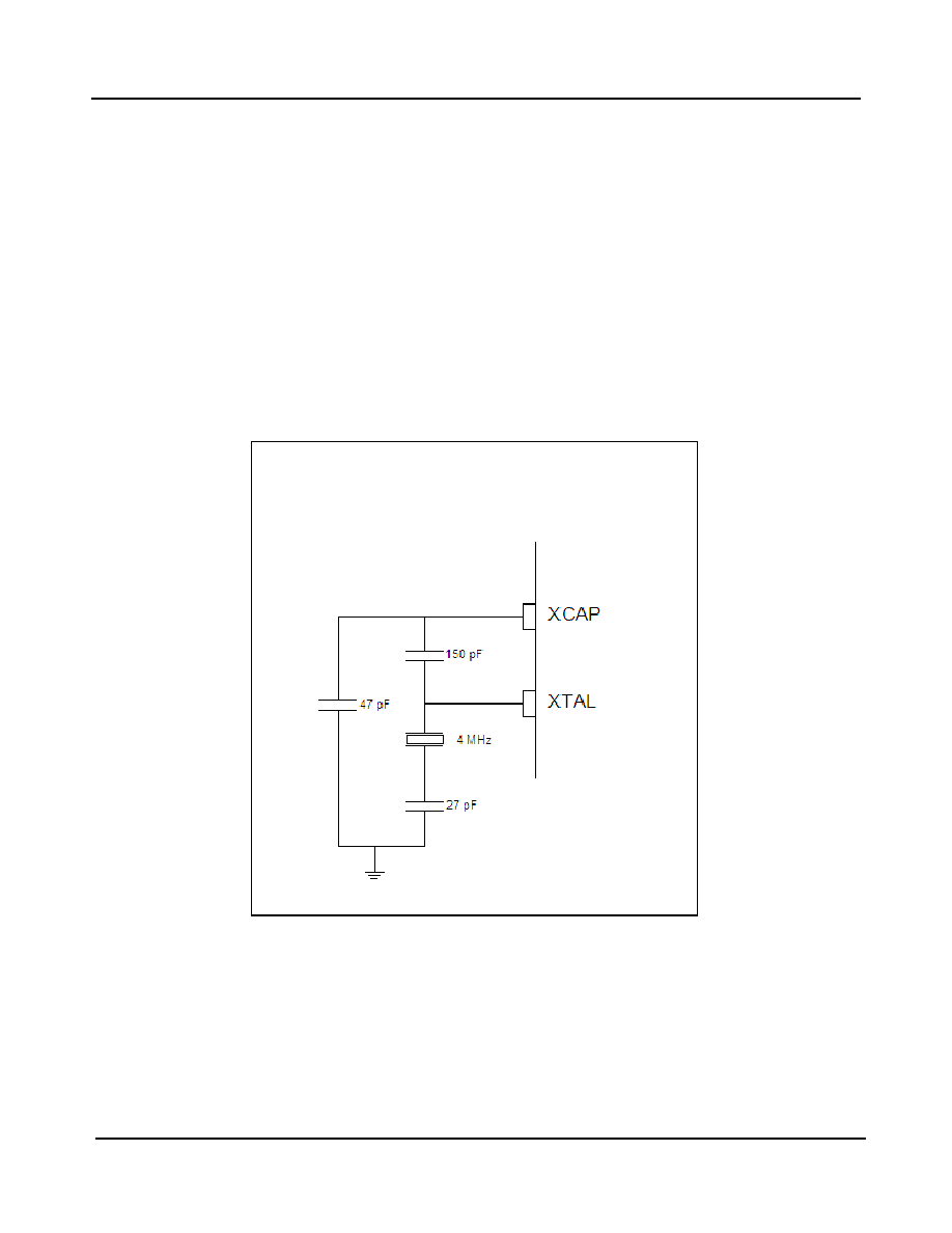
The crystal oscillator can also provide a clock signal to the demodulator. This can be done by taking the oscillator
signal from the crystal series capacitor (27 pF) as shown in the following diagram.
Figure 8 - Crystal Oscillator Circuit (4 MHz)

ZL10060
Data Sheet
22
Zarlink Semiconductor Inc.
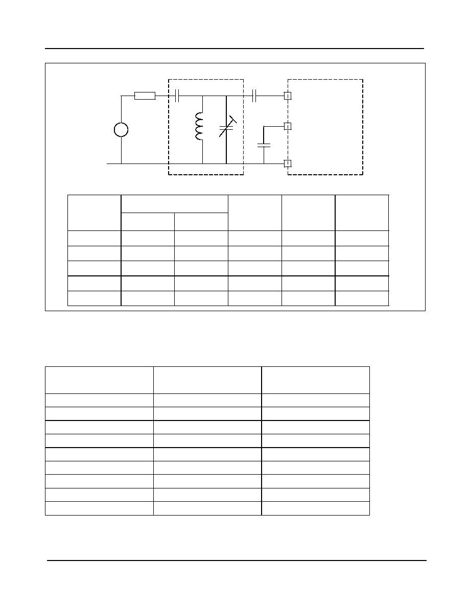
The interstage filter between the converter outputs provides some rejection of adjacent channels (N +/- 2).The
recommended values are shown in Figure 9. The choice of components is important not only to give a flat response
but also to provide an impedance transformation.
The specified noise figure for the low and mid bands assumes that there will be a network before the device to provide
image rejection. In a tuner this would be part of the input tracking filters but for test purposes a network is shown in
Figure 10.
Figure 9 - Interstage Filter
CNOPB
CNOP
SIPB
SIP
L1
L1
Cc
Cc
L2
C1
C1
Rterm
Rterm
SAWF Drive Amplifier Input
C2
R
sou
r
ce
R
sou
r
ce
Vcc
C1
Type
IF
0.5 dB
BW
Component values
MHz
MHz
R
source
R
term
L1
L2
C1
Cc
C2
0.5 dB Chebycheff
36
12
700
350
560
560
18
12
8.2
ZL10060
Data Sheet
23
Zarlink Semiconductor Inc.
The optimum charge pump and LO trim settings for the application circuit shown in Figure 8 are shown in the table
below. These give the optimum phase noise performance for the circuit shown. The changes in charge pump
current compensate for frequency and VCO gain variations.
Figure 10 - Noise Figure Measurement Conditions
Frequency Range
Charge Pump Setting
CP
LO Trim
LO1
VHF1 50 -110 MHz
01
1
VHF1 100 -160 MHz
10
1
VHF3 160 - 250 MHz
10
1
VHF3 250 - 350 MHz
01
0
VHF3 350 - 450 MHz
10
0
UHF 450 - 500 MHz
00
1
UHF 500 - 700 MHz
01
1
UHF 700 - 800 MHz
10
1
UHF 800 - 850 MHz
11
1
Table 23 - Optimum CP and LO Trim Settings
50
C1
L1
C2
IPREF
MIDIP/LOIP
Gnd
1nF
1nF
DUT
V
s
Band
Frequency
C1
L1
C2
LO
RF IN
MHz
MHz
pF
nH
pF
LOW
90
46
20
299
20
LOW
200
156
8
65
8
MID
240
196
8
41
8
MID
500
446
2.1
21
4
ZL10060
Data Sheet
24
Zarlink Semiconductor Inc.
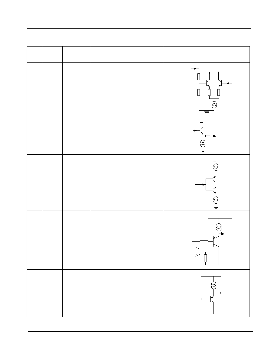
4.0 PIn Circuit Information
Pin
No.
Pin
Name
Port
Sense
Function
Schematic
1
IFAGC
Input
IF AGC control
2,
3
SAB,
SA
Output,
Output
SAW filter driver output A inverse
SAW filter driver output A
4
ADC
Input
ADC input
5
SDA
Bi-directional I
2
C bus serial data input/output
6
SCL
Input
I
2
C bus serial clock input
V
R EF
3K
3K
IFA G C
5 0
V c c
S A
S A B
V c c
A D C
V c c
S D A
V c c
S D A
V c c
S C L
ZL10060
Data Sheet
25
Zarlink Semiconductor Inc.
7
ADD
Input
I
2
C address select
8
AGCOP Output
AGC output
9,
10
CNOPB,
CNOP
Output,
Output
Converter Output inverse
Converter Output
11
Cont
-
Paddle
-
12
VccRF
Supply
RF section supply
-
13,
14
SIPB
SIP
Input,
Input
SAW filter driver input inverse,
SAW filter driver input
15
GPP0
Output
Switching port/Test output 1
Pin
No.
Pin
Name
Port
Sense
Function
Schematic
V c c
A D D
3 k
6 3 k
2 1 k
V c c
A G C O P
1 0 0
1 K
Vcc
CNOPB
CNOP
500
500
S IP
2 5 0
1 .1 K
V c c
S IP B
G P P 0
ZL10060
Data Sheet
26
Zarlink Semiconductor Inc.
16
GPP1
Output
Switching port/Test output 2
17
GPP2
Output
Switching port
As GPP1 (pin16)
18
VeeRF
Supply
RF section ground
-
19,
20,
21
LOIP
IPREF
MIDIP
Input,
Input,
Input
Low band input,
Mid- and Low-band i/p reference,
Mid-band input
22,
23
HIIP,
HIIPB
Input,
Input
Hi-band input,
Hi-band input inverse
24
GPP3
Output
Switching Port
As GPP1 (pin16)
25,
26
LLOP,
LLOPB
Output
Low band oscillator output,
Low-band oscillator output inverse
27,
28
LMOP,
LMOPB
Output,
Output
Mid-band oscillator output,
Mid-band oscillator output inverse
Pin
No.
Pin
Name
Port
Sense
Function
Schematic
G P P 1
G P P 2
G P P 3
1 0 K
V c c
IP R E F
LO IP
M ID IP
H IIP B
H IIP
LLOP
LLOPB
LMOP
LMOPB
ZL10060
Data Sheet
27
Zarlink Semiconductor Inc.
29,
30,
31,
32
LHIP,
LHOP,
LHOPB,
LHIPB
Input,
Output,
Output,
Input
High band oscillator input,
High-band oscillator output,
High-band oscillator output inverse,
High-band oscillator input inverse
33
VeeOSC Supply
LO ground
-
34
VccOSC Supply
LO supply
-
35,
36
IFIP,
IFIPB
Input,
Input
IF AGC amp input,
IF AGC amp input inverse
37,
38
DRIVE,
PUMP
Output,
Output
Loop amplifier drive output,
Loop amp charge pump output
39
VccDIG Supply
Digital section supply
-
40,
41
SD,
SDB
Output,
Output
SAW filter driver output D,
SAW filter driver o/p D inverse
42
VccIF
Supply
SAWF output supply
-
43
XCAP
Input
Reference osc feedback input
44
XTAL
Output
Reference osc crystal drive
See XCAP (pin 43)
Pin
No.
Pin
Name
Port
Sense
Function
Schematic
Vcc
LHIP
LHIPB
350
350
LHOPB
LHOP
IF IP B
IF IP
PUMP
340
Vcc
DRIVE
5 0
V c c
S D
S D B
0 .2 m A
1 1 0
X T A L
X C A P
V c c
ZL10060
Data Sheet
28
Zarlink Semiconductor Inc.
45
VccIF
Supply
IF AGC supply
-
46
VeeIF
Supply
IF AGC ground
-
47,
48
IFOP,
IFOPB
Output,
Output
IF AGC amp output,
IF AGC amp inverse output
Paddle Vee
-
-
-
Pin
No.
Pin
Name
Port
Sense
Function
Schematic
IF O P
V c c
ZL10060
Data Sheet
29
Zarlink Semiconductor Inc.
5.0 Absolute Maximum Ratings
All voltages are referred to V
ee
at 0 V.
6.0 Operating Range
All voltages are referred to V
ee
at 0 V.
Characteristic
Min.
Max.
Units
Conditions
Supply voltage
-0.3
6
V
RF input voltage
117
dB
�
V Transient condition only
Maximum voltage on SDA, SCL
5.5
V
V
cc
= 0 to 5.5V
Max voltage on all remaining signal pins
-0.3
V
cc
+0.3
V
The voltage on any pin must not exceed 6 V
Total port current
20
mA
Storage temperature
-55
150
o
C
Junction temperature
125
o
C
Power applied
Package thermal resistance
(chip to ambient)
27
o
C/W Package paddle soldered to ground
ESD protection
2.0
kV
All pins except 9,10
Mil-std 883B method 3015 cat1
1.25
kV
Pins 9, 10 only
Characteristic
Min.
Max.
Units.
Conditions
Supply voltage
4.5
5.5
V
Functional operation,
specification not guaranteed
Supply voltage
4.75
5.25
V
Full specification
Ambient Temperature
-20
85
o
C
Low Band Input Frequency
50
170
MHz
Mid Band Input Frequency
140
460
MHz
High Band Input Frequency
400
900
MHz
ZL10060
Data Sheet
30
Zarlink Semiconductor Inc.
7.0 Electrical Characteristics
Test conditions (unless otherwise stated). T = 25
o
C, V
ee
= 0 V, V
cc
= 5 V, IF Frequency = 36 MHz. All signals are differential with the exception of
VHF1 and VHF3 inputs.
Characteristic
Min.
Typ.
Max.
Units
Conditions
Supply current
Normal operation
117
140
mA
Total Current � UHF band
All switching ports off
All sections active
110
134
mA
Total Current - VHF Bands
All switching ports off
All sections active except
AGC IF amplifier
92
mA
UHF Band. Switching ports off
85
mA
VHF Bands. Switching ports off
Sleep Mode
9
mA
Crystal oscillator and data interface
enabled
33
mA
PLL and crystal oscillator enabled
Composite system to SAW Filter driver outputs
VHF1 Band
Conversion gain
29
32
35
dB
RFin = 54 MHz. Single ended input
Conversion gain
29
32
35
dB
RFin = 155 MHz. Single ended input
Noise Figure
9
11
dB
Rs = 50
,
SSB with input matching
network. See Figure 10.
OPIP3
135
146
dB
�
V
Two output tones at 110 dB
�
V
Output level causing 1%
cross modulation
113
120
dB
�
V
Note 2
Output level causing 1.5 kHz
FM
113
120
dB
�
V
Note 3
I
2
C bus transmission induced
LO frequency modulation
2.5
kHz
Transmission repetition rate of 20
msec minimum with no change to
previously loaded data, at 100 kHz
SCL rate
N+5 Direct modulation of
VCO
-40
dBc
Local oscillator sidebands induced by
an input carrier at 80 dB
�
V offset from
local oscillator by 100 kHz
Supply ripple spurious
-40
dBc
Residual FM induced on local
oscillator by 20 mV
p-p
ripple on V
cc
at
500 kHz
Local oscillator leakage to
any band input
30
dB
�
V
ZL10060
Data Sheet
31
Zarlink Semiconductor Inc.
IPIP2
134
143
dB
�
V
Two input tones at 87 dB
�
V at
90 MHz and 66 MHz with local
oscillator at 114 MHz
IPIP3
112
120
dB
�
V
Desired = 54 MHz at 45 dB
�
V
Undesired = 60 and 72 MHz at
87 dB
�
V
IPIP3
112
119
dB
�
V
Desired = 155 MHz at 45 dB
�
V
Undesired = 161 and 173 MHz at
87 dB
�
V
P1dB
93
106
dB
�
V
Output Impedance
100
10
nH
Phase Noise, SSB
PLL Loop Bandwidth ~ 3 kHz
f
comp
= 166.7 kHz
1 kHz
-90
-70
dBc/Hz
10 kHz
-95
-86
dBc/Hz
100 kHz
-115
-106
dBc/Hz
10 MHz
-135
dBc/Hz
Noise Floor
Reference spurs
-90
-50
dBc
Phase Noise, SSB
Narrow PLL Loop Bandwidth
f
comp
= 62.5 kHz
10 kHz
-97
dBc/Hz
100 kHz
-115
dBc/Hz
Composite system to SAW Filter driver outputs
VHF3 Band
Conversion gain
29
32
35
dB
RFin = 164 MHz Single ended input
Conversion gain
29
32
35
dB
RFin = 442 MHz Single ended input
Noise Figure
9
11
dB
Rs = 50
,
SSB with input matching
network. See Figure 10.
OPIP3
135
146
dB
�
V
Two output tones at 110 dB
�
V
Output level causing 1%
cross modulation
113
120
dB
�
V
Note 2
Output level causing 1.5 kHz
FM
113
120
dB
�
V
Note 3
Characteristic
Min.
Typ.
Max.
Units
Conditions
ZL10060
Data Sheet
32
Zarlink Semiconductor Inc.
I
2
C bus transmission induced
LO frequency modulation
2.5
kHz
Transmission repetition rate of 20
msec minimum with no change to
previously loaded data, at 100 kHz
SCL rate
N+5 Direct modulation of
VCO
-
-40
dBc
Local oscillator sidebands induced by
an input 750 MHz carrier at 80 dB
�
V
offset from local oscillator by 100 kHz.
Supply ripple spurious
-40
dBc
Residual FM induced on local
oscillator by 20 mV
p-p
ripple on V
cc
at
500 kHz
Local oscillator leakage to
any band input
30
dB
�
V
IPIP2
134
143
dB
�
V
Two input tones at 89 dB
�
V at
198 MHz and 398 MHz with local
oscillator at 240 MHz
IPIP3
112
122
dB
�
V
Desired = 165 MHz at 45 dB
�
V
Undesired = 171 and 183 MHz at
89 dB
�
V
IPIP3
112
119
dB
�
V
Desired = 438 MHz at 45 dB
�
V
Undesired = 444 and 456 MHz at
89 dB
�
V
P1dB
-95
107
dB
�
V
Output Impedance
100
10
nH
Phase Noise, SSB
PLL Loop Bandwidth ~ 3 kHz
f
comp
= 166.7 kHz
1 kHz
-87
-70
dBc/Hz
10 kHz
-92
-86
dBc/Hz
100 kHz
-114
-106
dBc/Hz
10 MHz
-135
dBc/Hz
Noise Floor
Reference spurs
-90
-50
dBc
Phase Noise, SSB
Narrow PLL Loop Bandwidth
f
comp
= 62.5 kHz
10 kHz
-94
dBc/Hz
100 kHz
-114
dBc/Hz
Composite system to SAW Filter driver outputs
UHF Band
Conversion gain
35
38
41
dB
RFin = 450 MHz
Characteristic
Min.
Typ.
Max.
Units
Conditions
ZL10060
Data Sheet
33
Zarlink Semiconductor Inc.
Conversion gain
35
38
41
dB
RFin = 866 MHz
Noise Figure
6
8
dB
Rs = 50
,
No image correction
OPIP3
135
146
dB
�
V
Two output tones at 110 dB
�
V
Output level causing 1%
cross modulation
113
120
dB
�
V
Note 2
Output level causing 1.5 kHz
FM
113
120
dB
�
V
Note 3
I
2
C bus transmission induced
LO frequency modulation
2.5
kHz
Transmission repetition rate of
20 msec minimum with no change to
previously loaded data, at 100 kHz
SCL rate
N+5 Direct modulation of
VCO
-30
dBc
Local oscillator sidebands induced by
an input 750 MHz carrier at 80 dB
�
V
offset from local oscillator by 100 kHz
Supply ripple spurious
-40
dBc
Residual FM induced on local
oscillator by 20 mV
p-p
ripple on V
cc
at
500 kHz
Local oscillator leakage to
any band input
60
dB
�
V
IPIP2
125
159
dB
�
V
Two input tones at 89 dB
�
V at
198 MHz and 398 MHz with local
oscillator at 240 MHz
IPIP3
108
115
dB
�
V
Desired = 438 MHz at 45 dB
�
V
Undesired = 444 and 456 MHz at
85 dB
�
V
IPIP3
108
112
dB
�
V
Desired = 858 MHz at 45 dB
�
V
Undesired = 864 and 876 MHz at
85 dB
�
V
P1dB
91
99
dB
�
V
Output Impedance
100
10
nH
Phase Noise, SSB
PLL Loop Bandwidth ~ 3 kHz
f
comp
= 166.7 kHz
1 kHz
-78
-70
dBc/Hz
10 kHz
-89
-84
dBc/Hz
100 kHz
-113
-106
dBc/Hz
10 MHz
-135
dBc/Hz
Noise Floor
Reference spurs
-80
-50
dBc
Characteristic
Min.
Typ.
Max.
Units
Conditions
ZL10060
Data Sheet
34
Zarlink Semiconductor Inc.
Phase Noise, SSB
Narrow PLL Loop Bandwidth
f
comp
= 62.5 kHz
10 kHz
-91
dBc/Hz
100 kHz
-113
dBc/Hz
AGC Detector and ADC
Operating frequency range
16
72
MHz
AGC Threshold Level
120
dB
�
V
AT[2:0] = 0
ADC leakage current
60
nA
V
ADC
= 4.0 V
-60
nA
V
ADC
= 0.5V
AGC source current
6.8
10
13.3
�
A
See Table 15
0.25
0.33
0.43
�
A
AGC sink current
-65
-100
-145
�
A
AGC attack current, triggered by
detected level exceeding AGC attack
point
AGC sink current 90% rise
and fall time
1
�
sec
AGC input level response
1
dB
Change in input level for AGC sink
current to change from high
impedance to 90% of maximum
value, with AGC operative
AGCOP output impedance
20
M
AGC inactive
AGCOP output voltage range
0.5
V
Minimum gain required
4
V
Maximum gain required
External AGC voltage
0.5
V
cc
-0.4
V
Maximum external voltage range
which can be applied to AGCOP
when disabled
AGCOP leakage current
-50
50
nA
Over normal operating range
ADC step size, LSB
0.16V
c
c
V
See Table 22
ADC step size accuracy
0.01V
c
c
V
See Table 22
AGCout_flag
High threshold
V
cc
-
0.66
V
AGF flag set to 1
AGCout_flag
Low threshold
V
cc
-
0.76
AGF flag set to 0
Characteristic
Min.
Typ.
Max.
Units
Conditions
ZL10060
Data Sheet
35
Zarlink Semiconductor Inc.
IF amplifier
Supply Current
25
mA
Frequency range
16
72
MHz
Input impedance
1.5
2
2.8
k
1.5
pF
Gain
(Voltage conversion gain,
differential source to
maximum load as defined
below)
61
66
70
dB
V
IFAGC
= 3.0 V
48
57
65
dB
V
IFAGC
= 2.2 V
21
25
29
dB
V
IFAGC
= 1.2 V
8
17
22
dB
V
IFAGC
= 0.5 V
Noise Figure
6.3
8.5
Rs=50
AGC range
41
48
dB
AGC control slope
25
31
38
dB/V
1.2
V
AGC
2.2
AGC input current
50
�
A
Gain variation within channel
0.25
dB
Channel bandwidth 8 MHz within
operating frequency range, with
maximum load as defined below
OPIP3
130
141
dB
�
V
Two output tones at 109 dB
�
V within
output channel
Gain range = 21 dB to maximum
Output impedance
120
Maximum load condition
4.7
k
Differential load
15
pF
I
2
C BUS
SDA SCL
Input high voltage
2.55
5.5
V
Input low voltage
0
1.4
V
Input current High
10
�
A
V
in
=5.5 V, V
cc
=5.25 V
10
�
A
V
in
=5.5 V, V
cc
=0 V
Input Current Low
-10
�
A
V
in
= 0 V, V
cc
=5.25 V
Hysteresis
0.4
V
SDA output voltage
0.4
V
I
sink
=3 mA
0.6
V
I
sink
=6 mA
SCL clock rate
100
kHz
Characteristic
Min.
Typ.
Max.
Units
Conditions
ZL10060
Data Sheet
36
Zarlink Semiconductor Inc.
Note 1: 0 dBm =107 dB
�
V. All input levels are specified as voltage that would be present if input signal generator was terminated in
50 ohms
Note 2: Wanted signal (picture carrier) = 101 dBmV at output. Undesired signal (sound carrier) at 5.25 MHz offset modulated with
1 kHz 80% AM. Increase undesired signal to give 1% AM on wanted signal.
Note 3: Wanted signal at 101 dBmV. Unwanted signal at 5.25 MHz offset modulated with 1 kHz 50% AM. Increase undesired signal to
give 1.5 kHz FM on wanted signal
Note 4: Current into PUMP pin with 20
�
A current from DRIVE pin
ADD (address) select
See Table 4
Input high current
1
mA
V
in
=V
ccD
Input low current
-0.5
mA
V
in
=V
ee
PLL Synthesizer
Charge pump output current
See Table 8
V
PUMP
=2 V
Charge pump output leakage
+-3
�10
nA
Note 4
Charge pump drive output
current
0.5
mA
V
DRIVE
=0.7 V
Crystal frequency
4
16
MHz
Application as in Figure 13 with
4 MHz crystal
Recommended crystal series
ESR
25
70
150
4 MHz parallel resonant crystal
External reference input
frequency
4
20
MHz
Sine wave coupled through 10 nF
capacitor
External reference drive level
0.2
2
V
pp
Sine wave coupled through 10nF
capacitor
0.5
V
pp
Recommended level for optimum
phase noise at 4 MHz
Phase detector comparison
frequency
31.25
250
kHz
RF division ratio
240
32767
Switching ports GPP3-GPP0
Sink current
10
mA
V
port
= 0.4
Pull up resistor GPP3- GPP1
10
k
Leakage current
10
�
A
V
port
= V
cc,
Port P0 only
Characteristic
Min.
Typ.
Max.
Units
Conditions
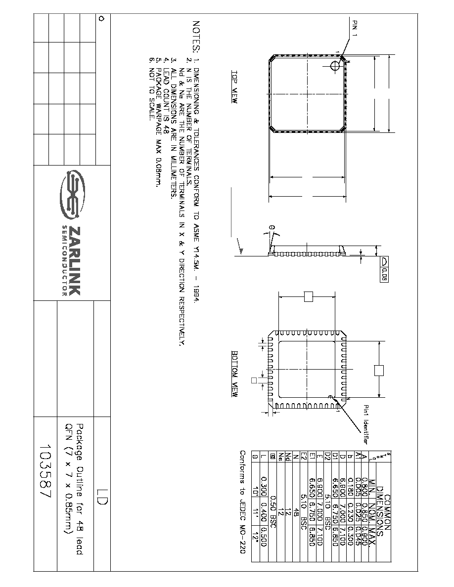
c Zarlink Semiconductor 2003 All rights reserved.
APPRD.
ISSUE
DATE
ACN
Package Code
Previous package codes
SEATING PLANE
1
25-02-2004
E1
E
E2
A1
A
D
D1
D2
b
e
L

www.zarlink.com
Information relating to products and services furnished herein by Zarlink Semiconductor Inc. or its subsidiaries (collectively "Zarlink") is believed to be reliable.
However, Zarlink assumes no liability for errors that may appear in this publication, or for liability otherwise arising from the application or use of any such
information, product or service or for any infringement of patents or other intellectual property rights owned by third parties which may result from such application or
use. Neither the supply of such information or purchase of product or service conveys any license, either express or implied, under patents or other intellectual
property rights owned by Zarlink or licensed from third parties by Zarlink, whatsoever. Purchasers of products are also hereby notified that the use of product in
certain ways or in combination with Zarlink, or non-Zarlink furnished goods or services may infringe patents or other intellectual property rights owned by Zarlink.
This publication is issued to provide information only and (unless agreed by Zarlink in writing) may not be used, applied or reproduced for any purpose nor form part
of any order or contract nor to be regarded as a representation relating to the products or services concerned. The products, their specifications, services and other
information appearing in this publication are subject to change by Zarlink without notice. No warranty or guarantee express or implied is made regarding the
capability, performance or suitability of any product or service. Information concerning possible methods of use is provided as a guide only and does not constitute
any guarantee that such methods of use will be satisfactory in a specific piece of equipment. It is the user's responsibility to fully determine the performance and
suitability of any equipment using such information and to ensure that any publication or data used is up to date and has not been superseded. Manufacturing does
not necessarily include testing of all functions or parameters. These products are not suitable for use in any medical products whose failure to perform may result in
significant injury or death to the user. All products and materials are sold and services provided subject to Zarlink's conditions of sale which are available on request.
Purchase of Zarlink's I
2
C components conveys a licence under the Philips I
2
C Patent rights to use these components in and I
2
C System, provided that the system
conforms to the I
2
C Standard Specification as defined by Philips.
Zarlink, ZL and the Zarlink Semiconductor logo are trademarks of Zarlink Semiconductor Inc.
Copyright Zarlink Semiconductor Inc. All Rights Reserved.
TECHNICAL DOCUMENTATION - NOT FOR RESALE
For more information about all Zarlink products
visit our Web Site at