
SEMICMF.017
1
Features
∑
Single chip synthesised downconverter forming a
complete double conversion tuner when
combined with the SL2100 or SL2101
∑
Compatible with digital and analogue system
requirements
∑
CTB contribution < -64 dBc, CXM contribution
< -62 dBc and spectral spread < -64 dBc
∑
IF amplifier optimised to interface with standard
SAW filters
∑
Extremely low phase noise balanced local
oscillator with I2C bus controlled band switching
and with very low fundamental and harmonic
radiation
∑
Integral fast mode compliant I2C bus controlled
PLL frequency synthesiser designed for high
comparison frequencies and low phase noise
performance
∑
Full ESD protection. (Normal ESD handling
procedures should be observed)
Applications
∑
Double conversion tuners
∑
Digital Terrestrial tuners
∑
Cable Modems
∑
Data transmit systems
∑
Data communications systems
∑
MATV
Description
The ZL10100 is a fully integrated single chip mixer
oscillator with on-board low phase noise I2C bus
controlled PLL frequency synthesiser. It is intended
primarily as the down converter for application in
double conversion tuners and is compatible with HIIF
frequencies between 1 and 1.3 GHz and all standard
tuner IF output frequencies.
The device contains all elements necessary, with the
exception of local oscillator tuning network, loop filter
and crystal reference to fabricate a complete
synthesised block converter with IF amplifier,
compatible with digital and analogue requirements.
DS5736
Issue 1.4
July 2002
Ordering Information
ZL10100/DDA
(Tubes)
ZL10100/DDB
(Tape & Reel)
-40∞C to 85∞C
ZL10100
Single Chip Synthesised
Downconverter with IF Amplifier
Data Sheet
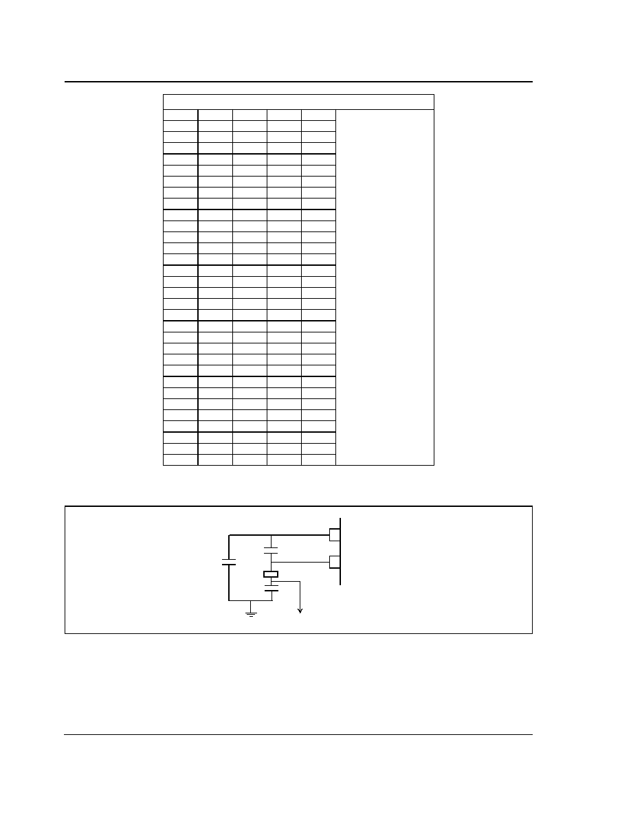
Figure 1 - ZL10100 Functional Block Diagram
RF Input
RF InputB
IF Output
IF OutputB
VCO
LO
LOB
Charge
Pump
15 Bit
Programmable
Divider
Pump
Drive
fpd/
2
I2C Bus
Interface
SDA
SCL
ADD
Reference Divider
REF
OSC
Port P0
Fpd/2
Fcomp
XTAL
XTALCAP

ZL10100
Data Sheet
2
SEMICMF.017
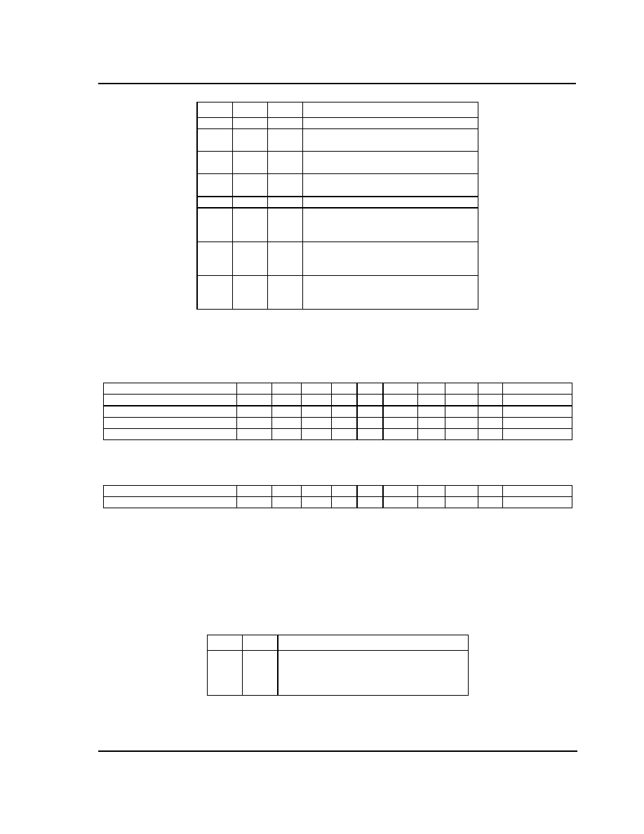
Pin Description
Figure 2 - Pin Description
Quick Reference Data
All data applies with the following conditions unless otherwise stated;
a) Output load of 150
, differential
b) Input spectrum of 5 channels centred on 1220 MHz, each carrier @ 77 dB
µV
Characteristic
Units
RF input operating range
1-1.3
GHz
IF output operating range
30-60
MHz
Input noise figure, SSB
9
dB
Conversion gain, diff to diff
24
dB
CTB
< -66
dBc
CXM
< -63
dBc
Spectral spread
< -70
dBc
Local oscillator phase noise
SSB @ 10 kHz offset
SSB @ 100 kHz offset
c -93
c-115
dBc/Hz
dBc/Hz
Local oscillator phase noise floor
-136
dBc/Hz
IF output impedance, differential
150
PLL phase noise at phase detector, 1 MHz comparison
frequency
-152
dBc/Hz
IFOUTPUTB
Vee
VccRF
Vee
RFINPUTB
RFINPUT
Vee
Vee
VccD
Vee
SCL
SDA
XTAL
XTAL CAP
IFOUTPUT
Vee
VccIF
Vee
VccLO
LO
LOB
VccLO
Vee
ADD
Vee
Port P0
DRIVE
PUMP
1
2
3
4
5
6
7
8
9
10
11
12
13
14
15
16
17
18
19
20
28
27
26
25
24
23
22
21

Data Sheet
ZL10100
3
SEMICMF.017
1.0
Functional Description
The ZL10100 is a bipolar, broadband wide dynamic range mixer oscillator with on-board I2C bus controlled PLL
frequency synthesiser, optimised for application as the down converter in double conversion tuner systems. It
also has application in any system where a wide dynamic range broadband synthesised frequency converter is
required.
The ZL10100 is a single chip solution containing all necessary active circuitry and simply requires an external
tuneable resonant network for the local oscillator sustaining network. The pin assignment is contained in the
the block diagram in Figure 1 and the Pin Description in Figure 2.
1.1
Converter section
In normal application the HIIF input is interfaced through appropriate impedance matching to the device input.
The RF input preamplifier of the device is designed for low noise figure, within the operating region of 1 to 1.3
GHz and for high intermodulation distortion intercept so offering good signal to noise plus composite distortion
spurious performance when loaded with a multi carrier system. The preamplifier also provides gain to the mixer
section and back isolation from the local oscillator section. The typical RF input impedance and matching
network for matching to a 1220 MHz HIIF filter, type B1603 are contained in Figures 3 and 4.
The output of the preamplifier is fed to the mixer section which is optimised for low radiation application. In this
stage the RF signal is mixed with the local oscillator frequency, which is generated by the on-board oscillator.
The oscillator block uses an external tuneable network and is optimised for low phase noise. The typical
application is shown in Figure 5, and the phase noise performance in Figure 6. This block interfaces direct with
the internal PLL to allow for frequency synthesis of the local oscillator.
The output of the mixer is internally coupled to a differential IF amplifier, which provides further gain and
provides for a 150
, differential output impedance and drive capability. The IF amplifier allows for IF
frequencies between 30 and 60 MHz.
The typical IF output impedance is contained in Figure 7.
The typical key performance data at 5V Vcc and 25 deg C ambient are shown in the Quick Reference Data
section on Page 2.
1.2
Local Oscillator
To maximise the local oscillator phase noise performance, the application circuit as in Figure 5 must be
carefully adhered to including the component type and manufacture where applicable, strip line dimension and
board material. Any deviation from these parameters may adversely affect phase noise characteristics and so
will require re-optimisation.
1.3
PLL frequency Synthesiser
The PLL frequency synthesiser section contains all the elements necessary, with the exception of a reference
frequency source and loop filter to control the oscillator, so forming a complete PLL frequency synthesised
source. The device allows for operation with a high comparison frequency and is fabricated in high speed logic,
which enables the generation of a loop with good phase noise performance.
The LO signal from the oscillator drives an internal preamplifier, which provides gain and reverse isolation from
the divider signals. The output of the preamplifier interfaces direct with the 15-bit fully programmable divider.
The programmable divider is of MN+A architecture, where the dual modulus prescaler is 16/17, the A counter is
4-bits, and the M counter is 11 bits.
The output of the programmable divider is fed to the phase comparator where it is compared in both phase and
frequency domain with the comparison frequency. This frequency is derived either from the on-board crystal
controlled oscillator or from an external reference source. In both cases the reference frequency is divided
down to the comparison frequency by the reference divider which is programmable into 1 of 29 ratios as
detailed in Table 1. The typical application for the crystal oscillator is contained in Figure 8 which also
demonstrates how a 4 MHz reference signal can be coupled out to a further PLL frequency synthesiser, such as
the upconverter section in a double conversion tuner.

ZL10100
Data Sheet
4
SEMICMF.017
The output of the phase detector feeds a charge pump and loop amplifier, which when used with an external
loop filter and high voltage transistor, integrates the current pulses into the varactor line voltage, used for
controlling the oscillator.
The programmable divider output Fpd divided by two and the reference divider output Fcomp can be switched
to port P0 by programming the device into test mode. The test modes are described in Table 2.
2.0
Programming
The ZL10100 is controlled by an I2C data bus and is compatible with both standard and fast mode formats.
Data and Clock are fed in on the SDA and SCL lines respectively as defined by I2C bus format. The device can
either accept data (write mode), or send data (read mode). The LSB of the address byte (R/W) sets the device
into write mode if it is low, and read mode if it is high. Tables 3, 4 and 5 illustrate the format of the data. The
device can be programmed to respond to several addresses, which enables the use of more than one device in
an I2C bus system. Table 5 shows how the address is selected by applying a voltage to the 'ADD' input. When
the device receives a valid address byte, it pulls the SDA line low during the acknowledge period, and during
following acknowledge periods after further data bytes are received. When the device is programmed into read
mode, the controller accepting the data must pull the SDA line low during all status byte acknowledge periods
to read another status byte. If the controller fails to pull the SDA line low during this period, the device
generates an internal STOP condition, which inhibits further reading.
2.1
Write mode
With reference to Table 5, bytes 2 and 3 contain frequency information bits 214-20 inclusive. Byte 4 controls the
synthesiser reference divider ratio, see Table 1 and the charge pump setting, see Table 6. Byte 5 controls the
test modes, see Table 2 and the output port P0.
After reception and acknowledgement of a correct address (byte 1), the first bit of the following byte determines
whether the byte is interpreted as a byte 2 or 4, a logic '0' indicating byte 2, and a logic '1' indicating byte 4.
Having interpreted this byte as either byte 2 or 4 the following data byte will be interpreted as byte 3 or 5
respectively. Having received two complete data bytes, additional data bytes can be entered, where byte
interpretation follows the same procedure, without re-addressing the device. This procedure continues until a
STOP condition is received. The STOP condition can be generated after any data byte, if however it occurs
during a byte transmission, the previous byte data is retained. To facilitate smooth fine tuning, the frequency
data bytes are only accepted by the device after all 15 bits of frequency data have been received, or after the
generation of a STOP condition.
2.2
Read mode
When the device is in read mode, the status byte read from the device takes the form shown in Table 4.
Bit 1 (POR) is the power-on reset indicator, and this is set to a logic '1' if the Vcc supply to the device has
dropped below 3V (at 25∞C), e.g., when the device is initially turned ON. The POR is reset to '0' when the read
sequence is terminated by a STOP command. When POR is set high this indicates that the programmed
information may have been corrupted and the device reset to the power up condition.
Bit 2 (FL) indicates whether the synthesiser is phase locked, a logic '1' is present if the device is locked, and a
logic '0' if the device is unlocked.

Data Sheet
ZL10100
5
SEMICMF.017
Figure 3 - Typical RF input impedance
Figure 4 - RF input impedance matching network to B1603 HIIF filter
Programmable Features
Synthesiser programmable divider
Function as described above.
Reference programmable divider
Function as described above.
Charge pump current
The charge pump current can be programmed by bits C1 and
C0 within data byte 4, as defined in Table 6.
Test mode
The test modes are defined by bits T2-T0 as described in
Table 2.
General purpose ports, P0
The general purpose port can be programmed by bits P0;
Logic '1' = on
Logic '0' = off (high impedance)
CH1
S 11
1 U FS
START 1 000.000 000 MHz
STOP 1 300.000 000 MHz
B1 4.7V
Cor
Avg
16
Smo
PRm
Z 0
50
26 Jun 2002 14:18:23
1
2
3
4
1_: 33.309
-74.777
2.1284 pF
1 000.000 000 MHz
2_: 29.262
-66.289
1.1 GHz
3_: 24.57
-58.744
1.22 GHz
4_: 22.332
-54.303
1.3 GHz
5
6
6
5
8.2 nH
2.7 pF
2.7 pF
ZL10100
B1603

ZL10100
Data Sheet
6
SEMICMF.017
Figure 5 - Oscillator Application
Figure 6 - Typical phase noise performance with application as in Figure 5
1 k
Varactor
line
BB555
4.3 nH
23
22
2 pF
-110
-105
-100
-95
-90
-85
-80
1010
1060
1110
1160
1210
LO Frequency (MHz)
P
hase noise (@ 10KHz offset),
dBc

Data Sheet
ZL10100
7
SEMICMF.017
Figure 7 - Typical IF output impedance single-ended
CH1
S 11
1 U FS
START 30.000 000 MHz
STOP 60.000 000 MHz
B1 PIN1 4.7V
Cor
Avg
16
Smo
PRm
Z 0
75
25 Jun 2002 06:58:03
1
2
3
4
1_: 76.695
-5.6172
944.45 pF
30.000 000 MHz
2_: 75.914
-7.2539
44 MHz
3_: 75.391
-7.9023
50 MHz
4_: 74.152
-9.207
60 MHz
ZL10100
Data Sheet
8
SEMICMF.017
Table 1. Reference Division Ratios
Figure 8 - Crystal oscillator application
R4
R3
R2
R1
R0
Ratio
0
0
0
0
0
2
0
0
0
0
1
4
0
0
0
1
0
8
0
0
0
1
1
16
0
0
1
0
0
32
0
0
1
0
1
64
0
0
1
1
0
128
0
0
1
1
1
256
0
1
0
0
0
Illegal state
0
1
0
0
1
5
0
1
0
1
0
10
0
1
0
1
1
20
0
1
1
0
0
40
0
1
1
0
1
80
0
1
1
1
0
160
0
1
1
1
1
320
1
0
0
0
0
Illegal state
1
0
0
0
1
6
1
0
0
1
0
12
1
0
0
1
1
24
1
0
1
0
0
48
1
0
1
0
1
96
1
0
1
1
0
192
1
0
1
1
1
384
1
1
0
0
0
Illegal state
1
1
0
0
1
7
1
1
0
1
0
14
1
1
0
1
1
28
1
1
1
0
0
56
1
1
1
0
1
112
1
1
1
1
0
224
1
1
1
1
1
448
Reference
47 pF
10 pF
XTALCAP
XTAL
47 pF
4 MHz
frequency
output
Data Sheet
ZL10100
9
SEMICMF.017
Table 2. Test modes
* clocks need to be present on crystal and local oscillator to enable
charge pump test modes and to toggle status byte bit FL
Table 3. Write data format (MSB is transmitted first)
Table 4. Read data format (MSB is transmitted first)
A
:
Acknowledge bit
MA1,MA0 :
Variable address bits (see Table 5)
2
14
-2
0
:
Programmable division ratio control bits
C1-C0
:
Charge pump current select (see Table 6)
R4-R0
:
Reference division ratio select (seeTable 1)
T2-T0
:
Test mode control bits (see Table 2)
P0
:
P0 port output state
POR
:
Power on reset indicator
FL
:
Phase lock flag
X
:
'Don't care'
Table 5. Address selection
# Programmed by connecting a 30 k
resistor between pin and Vcc
T2
T1
T0
Test Mode Description
0
0
0
Normal operation
0
0
1
Charge pump sink*
Status byte FL set to logic '0'
0
1
0
Charge pump source*
Status byte FL set to logic '0'
0
1
1
Charge pump disabled*
Status byte FL set to logic '1'
1
0
0
Normal operation and Port P0 = Fpd/2
1
0
0
Charge pump sink*
Status byte FL set to logic '0'
Port P0 = Fcomp
1
1
0
Charge pump source*
Status byte FL set to logic '0'
Port P0 = Fcomp
1
1
1
Charge pump disabled*
Status byte FL set to logic '1'
Port P0 = Fcomp
MSB
LSB
Address
1
1
0
0
0
MA1
MA0
0
A
Byte 1
Programmable divider
0
2
14
2
13
2
12
2
11
2
10
2
9
2
8
A
Byte 2
Programmable divider
2
7
2
6
2
5
2
4
2
3
2
2
2
1
2
0
A
Byte 3
Control data
1
C1
C0
R4
R3
R2
R1
R0
A
Byte 4
Control data
T2
T1
T0
X
X
X
0
P0
A
Byte 5
MSB
LSB
Address
1
1
0
0
0
MA1
MA0
1
A
Byte 1
Status Byte
POR
FL
0
0
0
0
0
0
A
Byte 2
MA1
MA0
Address Input Voltage Level
0
0
1
1
0
1
0
1
0-0.1 Vcc
Open circuit
0.4Vcc - 0.6 Vcc #
0.9 Vcc - Vcc
ZL10100
Data Sheet
10
SEMICMF.017
Table 6. Charge pump current
C1
C0
Current in
µ
A
min
typ
max
0
0
1
1
0
1
0
1
± 98
± 210
± 450
± 975
± 130
± 280
± 600
± 1300
± 162
± 350
± 750
± 1625
Electrical Characteristics - Test conditions (unless otherwise stated)
T
amb
= -40
∞C to 85∞C, Vee= 0V, Vcc=5V±5%. Input frequency 1220 MHz. IF output frequency 44 MHz.
These characteristics are guaranteed by either production test or design. They apply within the specified ambient temperature and supply
voltage unless otherwise stated.
Characteristic
Pin
Min
Typ
Max
Units
Conditions
Supply current
120
160
mA
Input frequency range
1
1.3
GHz
Composite peak input signal
86
dB
µ
V
Operating condition only.
Input impedance
See Figure 3.
Input Noise Figure
9
11
dB
Tamb = 27
∞C
Conversion gain
20
23
26
dB
Differential to differential
voltage gain to differential
150
load.
Gain variation within channel
0.5
dB
Channel bandwidth 8 MHz
within operating frequency
range.
Through gain
-30
dB
CTB
-64
dBc
See note 4.
CXM
-62
dBc
See note 4.
LO operating range
0.9
1.6
GHz
Maximum tuning range
determined by application,
see note (3), guaranteed by
design.
LO phase noise, SSB
@ 10 kHz offset
@ 100 kHz offset
-94
-116
-90
-110
dBc/Hz
dBc/Hz
See Figure 6.
Application as in Figure 5.
LO phase noise floor
-136
dBc/Hz Application as in Figure 5.
IF output frequency range
30
60
MHz
IF output impedance
75
Single-ended. See Figure 7.
IF output return loss
-20
d
See Figure 7, over operating
range.
All other spurs on IF Output
20
dB
µ
V
Within channel bandwidth of
8 MHz.
Data Sheet
ZL10100
11
SEMICMF.017
Notes
(1) When measuring from a 50
environment, the voltage step up transformation needs to be taken into account.
(2) Port powers up in high impedance state.
(3) To maximise phase noise the tuning range should be minimised and Q of resonator maximised. The application as in Figure 5 has a
tuning range of 200 MHz.
(4) Measured with 5 channels @ 77 dBuV centred on desired channel .
SYNTHESISER
SDA, SCL
Input high voltage
Input low voltage
Input high current
Input low current
Leakage current
Hysterysis
3
0
-10
0.4
5.5
1.5
10
10
V
V
µ
A
µ
A
µ
A
V
I2C 'Fast mode' compliant
Input voltage = Vcc
Input voltage = Vee
Vcc=Vee
SDA output voltage
0.4
0.6
V
V
Isink = 3 mA
Isink = 6 mA
SCL clock rate
400
kHz
Charge pump output current
±3
±10
nA
See Table 6.
Vpin = 2V
Charge pump drive output current
0.5
mA
Vpin = 0.7V
Crystal frequency
2
20
MHz
See Figure 8 for application.
Recommended crystal series
resistance
10
200
4 MHz parallel resonant
crystal
External reference input frequency
2
20
MHz
Sinewave coupled through
10 nF blocking capacitor
External reference drive level
0.2
0.5
Vpp
Sinewave coupled through
10 nF blocking capacitor
Phase detector comparison
frequency
4
MHz
Equivalent phase noise at phase
detector
-152
-158
dBc/Hz
dBc/Hz
SSB, within loop bandwidth
2 MHz
250 kHz
Local oscillator programmable divider
division ratio
240
32767
Reference division ratio
See Table 1.
Output port
sink current
leakage current
2
10
mA
µ
A
See note 2.
Vport = 0.7
Vport = Vcc
Address select
Input high current
Input low current
1
-0.5
mA
mA
See Table 5
Vin = Vcc
Vin = Vee
Electrical Characteristics - Test conditions (unless otherwise stated)
T
amb
= -40
∞C to 85∞C, Vee= 0V, Vcc=5V±5%. Input frequency 1220 MHz. IF output frequency 44 MHz.
These characteristics are guaranteed by either production test or design. They apply within the specified ambient temperature and supply
voltage unless otherwise stated.
Characteristic
Pin
Min
Typ
Max
Units
Conditions
ZL10100
Data Sheet
12
SEMICMF.017
Absolute Maximum Ratings -
All voltages are referred to Vee at 0V.
Characteristic
Min
Max
Units
Conditions
Supply voltage
-0.3
7
V
RF input voltage
117
dBuV
Differential
All I/O port DC offsets
-0.3
Vcc+0.3
V
SDA, SCL DC offsets
-0.3
6
V
Vcc = Vee to 5.25V
Storage temperature
-55
150
∞C
Junction temperature
150
∞C
Package thermal resistance, chip to case
20
∞C/W
Package thermal resistance, chip to case
80
∞C/W
Power consumption at 5.25V
700
mW
ESD protection
3.5
kV
Mil-std 883B method 3015 cat1
Data Sheet
ZL10100
13
SEMICMF.017
RF Inputs
Reference Oscillator
Oscillator Inputs
SDA/SCL (pins 12 and 11)
IF Outputs
Output Port
Loop Amplifier
ADD Input
Figure 9 - Input and Output Interface Circuits
RFINPUTB
RFINPUT
5
6
XTAL
XTALCAP
13
14
v
cc
200
µA
LO
LOB
23
22
V
REF
500K
500K
V
CC
SCL/SDA
500K
ACK
*
*
On SDA only
V
CC
75
75
28
1
IF Output
IF OutputB
PO
17
v
cc
Pump
220
16
15
Drive
v
cc
ADD
40K
120K
19
ZL10100
Data Sheet
14
SEMICMF.017
Figure 10 - ZL10100 Evaluation Board Schematic
VCC
C312
2.5pF
D301
BB555
VCC
R303
20K
R304
1K
C306
6.8nF
VCC
VCC
C316
100nF
C330
100nF
L311
4n3H
IF Output B
1
Vee
2
VccRF
3
Vee
4
RF Input B
5
RF Input
6
Vee
7
Vee
8
VccD
9
Vee
10
SCL
11
SDA
12
XTAL
13
XTAL CAP
14
PUMP
15
DRIVE
16
PORT P0
17
Vee
18
ADD
19
Vee
20
VccLO
21
LO B
22
LO
23
VccLO
24
Vee
25
VccLO
26
Vee
27
IF Output
28
IC1
ZL10100
C311
47pF
X301
4MHz
C310
47pF
C301
10pF
C307
33nF
C308
100pF
R307
24K
TR3011
BCW31
R306
22K
C305
100nF
+27V
R305
10R
R308
10R
C300
100nF
C318
100nF
L306
3u9H
L303
3u9H
VCC
C324
100nF
C303
27pF
C302
27pF
L312
10nH
R302
10K
SDA
SCL
XTAL pin (2)
R311
1K
C309
470nF
C342
10pF
C132
10pF
IF Output B /
IF Output /
1
2
5
6
4,8
SAW201
EPCOS B1603 SAW Filter
L201
6.8nH
VCC
L202
6.8nH
R200
33R
R201
33R
C201
1pF
R202
300R
R203
300R
IF output pin (14)
IF output pin (15)
Demodulator Input
Demodulator Input
From Zarlink SL2101 Up converter
From Zarlink SL2101 Up converter
To Zarlink SL2101 Up converter


www.zarlink.com
Information relating to products and services furnished herein by Zarlink Semiconductor Inc. trading as Zarlink Semiconductor or its subsidiaries (collectively
"Zarlink") is believed to be reliable. However, Zarlink assumes no liability for errors that may appear in this publication, or for liability otherwise arising from the
application or use of any such information, product or service or for any infringement of patents or other intellectual property rights owned by third parties which may
result from such application or use. Neither the supply of such information or purchase of product or service conveys any license, either express or implied, under
patents or other intellectual property rights owned by Zarlink or licensed from third parties by Zarlink, whatsoever. Purchasers of products are also hereby notified
that the use of product in certain ways or in combination with Zarlink, or non-Zarlink furnished goods or services may infringe patents or other intellectual property
rights owned by Zarlink.
This publication is issued to provide information only and (unless agreed by Zarlink in writing) may not be used, applied or reproduced for any purpose nor form part
of any order or contract nor to be regarded as a representation relating to the products or services concerned. The products, their specifications, services and other
information appearing in this publication are subject to change by Zarlink without notice. No warranty or guarantee express or implied is made regarding the
capability, performance or suitability of any product or service. Information concerning possible methods of use is provided as a guide only and does not constitute
any guarantee that such methods of use will be satisfactory in a specific piece of equipment. It is the user's responsibility to fully determine the performance and
suitability of any equipment using such information and to ensure that any publication or data used is up to date and has not been superseded. Manufacturing does
not necessarily include testing of all functions or parameters. These products are not suitable for use in any medical products whose failure to perform may result in
significant injury or death to the user. All products and materials are sold and services provided subject to Zarlink's conditions of sale which are available on request.
Purchase of Zarlink's I
2
C components conveys a licence under the Philips I
2
C Patent rights to use these components in an I
2
C System, provided that the system
conforms to the I
2
C Standard Specification as defined by Philips.
Zarlink, ZL and the Zarlink Semiconductor logo are trademarks of Zarlink Semiconductor Inc.
Copyright 2003, Zarlink Semiconductor Inc. All Rights Reserved.
TECHNICAL DOCUMENTATION - NOT FOR RESALE
For more information about all Zarlink products
visit our Web Site at