1
Zarlink Semiconductor Inc.
Zarlink, ZL and the Zarlink Semiconductor logo are trademarks of Zarlink Semiconductor Inc.
Copyright 2004, Zarlink Semiconductor Inc. All Rights Reserved.
Features
� Conforms to EBU specification for DVB-S and
DirecTV specification for DSS
� On-chip digital filtering supports 1 - 45 MSps
symbol rates
� On-chip 60 or 90 MHz dual-ADC
� High speed scanning mode for blind symbol
rate/code rate acquisition
� Automatic spectral inversion resolution
� High level software interface for minimum
development time
� Up to �22.5 MHz LNB frequency tracking
� DiSEqCTM v2.2: receive/transmit for full control of
LNB, dish and other components
� Compact 64-pin LQFP package (7 x 7 mm)
� A full DVB-S front-end reference design is
available, ref. ZLE10538
Applications
� DVB 1 - 45 MSps compliant satellite receivers
� DSS 20 MSps compliant satellite receivers
� SMATV (Single Master Antenna TV) trans-
modulators
� Satellite PC applications
Description
The ZL10313 is a QPSK/BPSK 1 - 45 MSps
demodulator and channel decoder for digital satellite
television transmissions to the European Broadcast
Union ETS 300 421 specification. It receives analogue
I and Q signals from the tuner, digitises and digitally
demodulates this signal, implements the complete
DVB/DSS FEC (Forward Error Correction) and de-
scrambling function. The output is in the form of
MPEG2 or DSS transport stream data packets. The
ZL10313 also provides automatic gain control to the RF
front-end device.
The ZL10313 has a serial 2-wire bus interface to the
control microprocessor. Minimal software is required to
control the ZL10313 because of the built in automatic
search and decode control functions.
November 2004
Ordering Information
ZL10313QCG
64 Pin LQFP
Trays, Bake & Drypack
ZL10313QCG1
64 Pin LQFP*
Trays, Bake & Drypack
ZL10313UBH
Die supplied in wafer form**
*Pb Free Matte Tin
**
Please contact Sales for further details
0
�
C to +70
�
C
ZL10313
Satellite Demodulator
Data Sheet
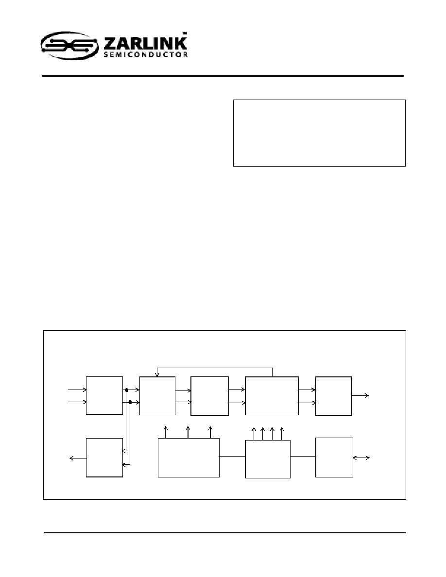
Figure 1 - Functional Block Diagram
I I/P
Q I/P
Dual ADC
De-rotator
Decimation
Filtering
Timing recovery
Matched filter
Phase recovery
MPEG/
DSS
Packets
Bus I/O
2-Wire Bus
Interface
Acquisition
Control
Clock Generation
Analog
AGC
Control
DVB
DSS
FEC

ZL10313
Data Sheet
2
Zarlink Semiconductor Inc.
Figure 2 - ZL10313 Pin Allocation
Notes: All supply pins must be connected as they are not all commoned internally.
Pin Table
No.
Name
No.
Name
No.
Name
No.
Name
1
Reset
17
CVdd
33
Gnd
49
MDO[1]
2
DiSEqC[2]
1
1. Can be programmed to be MICLK (MPEG input clock) instead.
18
Gnd
34
CVdd
50
CVdd
3
DiSEqC[1]
19
XTI
35
Addr[1]
51
Gnd
4
DiSEqC[0]
20
XTO
36
Addr[2]
52
MDO[2]
5
Vdd
21
Gnd
37
Addr[3]
53
MDO[3]
6
Gnd
22
CVdd
38
Addr[4]
54
Gnd
7
CVdd
23
Gnd
39
Vdd
55
Vdd
8
Gnd
24
Iin
40
Gnd
56
MDO[4]
9
Sleep
25
Iin
41
AGC
57
MDO[5]
10
CLK1
26
Gnd
42
Test
58
Gnd
11
DATA1
27
Vdd
43
IRQ
1
59
CVdd
12
CVdd
28
Gnd
44
CVdd
60
MDO[6]
13
Gnd
29
Qin
45
Gnd
61
MDO[7]
14
DATA2
30
Qin
46
MOSTRT
62
MOCLK
15
CLK2
31
Gnd
47
MOVAL
63
BKERR
16
OscMode
32
CVdd
48
MDO[0]
64
Status

ZL10313
Data Sheet
Table of Contents
3
Zarlink Semiconductor Inc.
1.0 Application Diagram . . . . . . . . . . . . . . . . . . . . . . . . . . . . . . . . . . . . . . . . . . . . . . . . . . . . . . . . . . . . . . . . . . . . 7
2.0 Functional Overview . . . . . . . . . . . . . . . . . . . . . . . . . . . . . . . . . . . . . . . . . . . . . . . . . . . . . . . . . . . . . . . . . . . . 8
2.1 Introduction . . . . . . . . . . . . . . . . . . . . . . . . . . . . . . . . . . . . . . . . . . . . . . . . . . . . . . . . . . . . . . . . . . . . . . . . . 8
2.2 Analogue-to-Digital Converter . . . . . . . . . . . . . . . . . . . . . . . . . . . . . . . . . . . . . . . . . . . . . . . . . . . . . . . . . . . 8
2.3 QPSK Demodulator . . . . . . . . . . . . . . . . . . . . . . . . . . . . . . . . . . . . . . . . . . . . . . . . . . . . . . . . . . . . . . . . . . . 8
2.4 Forward Error Correction. . . . . . . . . . . . . . . . . . . . . . . . . . . . . . . . . . . . . . . . . . . . . . . . . . . . . . . . . . . . . . . 9
2.4.1 Viterbi Error Count Measurement . . . . . . . . . . . . . . . . . . . . . . . . . . . . . . . . . . . . . . . . . . . . . . . . . . . 9
2.4.1.1 Viterbi Error Count Coarse Indication. . . . . . . . . . . . . . . . . . . . . . . . . . . . . . . . . . . . . . . . . . . 10
2.4.2 The Frame Alignment Block. . . . . . . . . . . . . . . . . . . . . . . . . . . . . . . . . . . . . . . . . . . . . . . . . . . . . . . 11
2.4.3 The De-Interleaver Block . . . . . . . . . . . . . . . . . . . . . . . . . . . . . . . . . . . . . . . . . . . . . . . . . . . . . . . . . 11
2.4.3.1 DVB . . . . . . . . . . . . . . . . . . . . . . . . . . . . . . . . . . . . . . . . . . . . . . . . . . . . . . . . . . . . . . . . . . . . 11
2.4.3.2 DSS . . . . . . . . . . . . . . . . . . . . . . . . . . . . . . . . . . . . . . . . . . . . . . . . . . . . . . . . . . . . . . . . . . . . 12
2.4.4 The Reed-Solomon Decoder Block . . . . . . . . . . . . . . . . . . . . . . . . . . . . . . . . . . . . . . . . . . . . . . . . . 13
2.4.5 The Energy Dispersal (de-scrambler) Block, DVB Only. . . . . . . . . . . . . . . . . . . . . . . . . . . . . . . . . . 14
2.4.6 Output Stage . . . . . . . . . . . . . . . . . . . . . . . . . . . . . . . . . . . . . . . . . . . . . . . . . . . . . . . . . . . . . . . . . . 14
2.5 Control . . . . . . . . . . . . . . . . . . . . . . . . . . . . . . . . . . . . . . . . . . . . . . . . . . . . . . . . . . . . . . . . . . . . . . . . . . . . 14
2.5.1 Symbol Rate and Code Rate Search Mode . . . . . . . . . . . . . . . . . . . . . . . . . . . . . . . . . . . . . . . . . . . 15
2.6 DiSEqC Transmit and Receive Messages . . . . . . . . . . . . . . . . . . . . . . . . . . . . . . . . . . . . . . . . . . . . . . . . 15
2.6.1 DiSEqC Transmitting Messages . . . . . . . . . . . . . . . . . . . . . . . . . . . . . . . . . . . . . . . . . . . . . . . . . . . 15
2.6.2 DiSEqC Receiving Messages . . . . . . . . . . . . . . . . . . . . . . . . . . . . . . . . . . . . . . . . . . . . . . . . . . . . . 16
3.0 Microprocessor Control . . . . . . . . . . . . . . . . . . . . . . . . . . . . . . . . . . . . . . . . . . . . . . . . . . . . . . . . . . . . . . . . 16
3.1 RADD: 2-wire Register Address (W) . . . . . . . . . . . . . . . . . . . . . . . . . . . . . . . . . . . . . . . . . . . . . . . . . . . . . 16
3.2 Primary 2-wire Bus Interface . . . . . . . . . . . . . . . . . . . . . . . . . . . . . . . . . . . . . . . . . . . . . . . . . . . . . . . . . . . 17
3.3 Secondary 2-wire Bus for Tuner Control . . . . . . . . . . . . . . . . . . . . . . . . . . . . . . . . . . . . . . . . . . . . . . . . . . 18
4.0 Electrical Characteristics . . . . . . . . . . . . . . . . . . . . . . . . . . . . . . . . . . . . . . . . . . . . . . . . . . . . . . . . . . . . . . . 18
4.1 Recommended Operating Conditions . . . . . . . . . . . . . . . . . . . . . . . . . . . . . . . . . . . . . . . . . . . . . . . . . . . . 18
4.2 Absolute Maximum Ratings. . . . . . . . . . . . . . . . . . . . . . . . . . . . . . . . . . . . . . . . . . . . . . . . . . . . . . . . . . . . 18
4.3 Primary 2-Wire Bus Timing . . . . . . . . . . . . . . . . . . . . . . . . . . . . . . . . . . . . . . . . . . . . . . . . . . . . . . . . . . . . 19
4.4 Crystal Specification . . . . . . . . . . . . . . . . . . . . . . . . . . . . . . . . . . . . . . . . . . . . . . . . . . . . . . . . . . . . . . . . . 20
4.5 Electrical Characteristics . . . . . . . . . . . . . . . . . . . . . . . . . . . . . . . . . . . . . . . . . . . . . . . . . . . . . . . . . . . . . . 20
4.6 ZL10313 Pinout Description . . . . . . . . . . . . . . . . . . . . . . . . . . . . . . . . . . . . . . . . . . . . . . . . . . . . . . . . . . . 22
4.7 Alphabetical Listing of Pin-Out . . . . . . . . . . . . . . . . . . . . . . . . . . . . . . . . . . . . . . . . . . . . . . . . . . . . . . . . . 24
5.0 References . . . . . . . . . . . . . . . . . . . . . . . . . . . . . . . . . . . . . . . . . . . . . . . . . . . . . . . . . . . . . . . . . . . . . . . . . . . 24
6.0 Trademarks. . . . . . . . . . . . . . . . . . . . . . . . . . . . . . . . . . . . . . . . . . . . . . . . . . . . . . . . . . . . . . . . . . . . . . . . . . . 24

ZL10313
Data Sheet
List of Figures
4
Zarlink Semiconductor Inc.
Figure 1 - Functional Block Diagram . . . . . . . . . . . . . . . . . . . . . . . . . . . . . . . . . . . . . . . . . . . . . . . . . . . . . . . . . . . . 1
Figure 2 - ZL10313 Pin Allocation . . . . . . . . . . . . . . . . . . . . . . . . . . . . . . . . . . . . . . . . . . . . . . . . . . . . . . . . . . . . . . 2
Figure 3 - ZL10313 Functional Block Diagram . . . . . . . . . . . . . . . . . . . . . . . . . . . . . . . . . . . . . . . . . . . . . . . . . . . . 5
Figure 4 - Typical Application Schematic . . . . . . . . . . . . . . . . . . . . . . . . . . . . . . . . . . . . . . . . . . . . . . . . . . . . . . . . . 7
Figure 5 - Viterbi Block Diagram . . . . . . . . . . . . . . . . . . . . . . . . . . . . . . . . . . . . . . . . . . . . . . . . . . . . . . . . . . . . . . . 9
Figure 6 - Viterbi Error Count Measurement . . . . . . . . . . . . . . . . . . . . . . . . . . . . . . . . . . . . . . . . . . . . . . . . . . . . . 10
Figure 7 - Viterbi Error Count Coarse Indication . . . . . . . . . . . . . . . . . . . . . . . . . . . . . . . . . . . . . . . . . . . . . . . . . . 11
Figure 8 - DVB Conceptual Diagram of the Convolutional De-Interleaver Block . . . . . . . . . . . . . . . . . . . . . . . . . . 12
Figure 9 - DSS Conceptual Diagram of the Convolutional De-Interleaver Block . . . . . . . . . . . . . . . . . . . . . . . . . . 12
Figure 10 - DVB Block Structure . . . . . . . . . . . . . . . . . . . . . . . . . . . . . . . . . . . . . . . . . . . . . . . . . . . . . . . . . . . . . . 13
Figure 11 - DVB Energy Dispersal Conceptual Diagram . . . . . . . . . . . . . . . . . . . . . . . . . . . . . . . . . . . . . . . . . . . . 13
Figure 12 - DVB Energy Dispersal Conceptual Diagram . . . . . . . . . . . . . . . . . . . . . . . . . . . . . . . . . . . . . . . . . . . . 14
Figure 13 - ZL10313 Control Structure . . . . . . . . . . . . . . . . . . . . . . . . . . . . . . . . . . . . . . . . . . . . . . . . . . . . . . . . . 15
Figure 14 - Primary 2-Wire Bus Timing . . . . . . . . . . . . . . . . . . . . . . . . . . . . . . . . . . . . . . . . . . . . . . . . . . . . . . . . . 19
Figure 15 - Crystal Oscillator Circuit . . . . . . . . . . . . . . . . . . . . . . . . . . . . . . . . . . . . . . . . . . . . . . . . . . . . . . . . . . . 20
ZL10313
Data Sheet
5
Zarlink Semiconductor Inc.
Overview
The ZL10313 is a QPSK/BPSK 1 - 45 MSps demodulator and channel decoder for digital satellite television
transmissions compliant to both DVB-S and DSS standards and other systems, such as LMDS, that use the same
architecture.
A Command Driven Control (CDC) system is provided making the ZL10313 very simple to program. After the tuner
has been programmed to the required frequency to acquire a DVB transmission, the ZL10313 requires a minimum
of five registers to be written.
The ZL10313 provides a monitor of bit error rate after the QPSK module and also after the Viterbi module. For
receiver installation, a high speed scan or 'blind search' mode is available. This allows all signals from a given
satellite to be evaluated for frequency, symbol rate and convolutional coding scheme. The phase of the IQ signals
can be automatically determined.
Full DiSEqC is provided for both writing and reading DiSEqC messages. Storage in registers for up to eight data
bytes sent and eight data bytes received is provided.
Figure 3 - ZL10313 Functional Block Diagram
I I/P
Q I/P
Dual ADC
De-rotator
Decimation
Filtering
Timing recovery
Matched filter
Phase recovery
MPEG/
DSS
Packets
Bus I/O
2-wire Bus
Interface
Acquisition
Control
Clock Generation
Analog
AGC
Control
DVB
DSS
FEC

ZL10313
Data Sheet
6
Zarlink Semiconductor Inc.
Additional Features
� 2-wire bus microprocessor interface
� All-digital clock and carrier recovery
� On-chip PLL clock generation using a low cost
10 to 16 MHz crystal (or external clock)
� 3.3/1.8 V operation
� 64 pin LQFP package
� Low external component count
� Commercial temperature range 0 to 70�C
� External MPEG clock option
Demodulator
� BPSK or QPSK programmable
� Optional fast acquisition mode for low symbol
rates
Viterbi
� Programmable decoder rates 1/2, 2/3, 3/4, 5/6,
6/7, 7/8
� Automatic spectrum resolution of IQ phase
� Constraint length k = 7
� Trace back depth 128
� Extensive SNR and BER monitors
De-Interleaver
� Compliant with DVB and DSS standards
Reed-Solomon
� (204, 188) for DVB and (146,130) for DSS
� Reed-Solomon bit-error-rate monitor to indicate
Viterbi performance
De-Scrambler
� EBU specification de-scrambler for DVB mode
Outputs
� MPEG transport parallel & serial output
� Three output clocking modes for maximum
flexibility
� Integrated MPEG2 TEI bit processing for DVB only
Application Support
� Windows based evaluation software
� ANSI-C compliant software
� A full DVB-S front-end satellite tuner reference
design kit is available for evaluation, based on the
schematic below (Figure 4). Zarlink reference
ZLE10538
ZL10313
Data Sheet
7
Zarlink Semiconductor Inc.
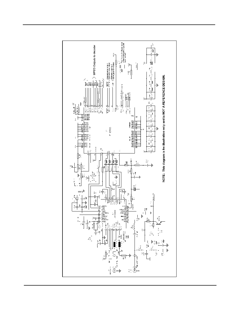
1.0 Application Diagram
Figure 4 - Typical Application Schematic

ZL10313
Data Sheet
8
Zarlink Semiconductor Inc.
2.0 Functional Overview
2.1 Introduction
ZL10313 is a single-chip variable rate digital QPSK/BPSK satellite demodulator and channel decoder. The
ZL10313 accepts base-band in-phase and quadrature analogue signals and delivers an MPEG or DSS packet data
stream. Digital filtering in ZL10313 removes the need for programmable external anti-alias filtering for all symbol
rates from 1 - 45 MSps. Frequency, timing and carrier phase recovery are all digital and the only feed-back to the
analogue front-end is for automatic gain control. The digital phase recovery loop enables very fine bandwidth
control that is needed to overcome performance degradation due to phase and thermal noise.
All acquisition algorithms are built into the ZL10313 controller. The ZL10313 can be operated in a Command Driven
Control (CDC) mode by specifying the symbol rate and Viterbi code rate. There is also a provision for a search for
unknown symbol rates and Viterbi code rates.
2.2 Analogue-to-Digital Converter
The A/D converters sample single-ended or differential analogue inputs and consist of a dual ADC and circuitry to
provide improved SiNaD (Signal-Noise and Distortion) and channel matching.
The fixed rate sampling clock is provided on-chip using a programmable PLL needing only a low cost 10 to 16 MHz
crystal. Different crystal frequencies can be combined with different PLL ratios, depending on the maximum symbol
rate, allowing a very flexible approach to clock generation. An external clock signal in the range 4 to 16 MHz can
also be used as the master clock.
2.3 QPSK Demodulator
The demodulator in the ZL10313 consists of signal amplitude offset compensation, frequency offset compensation,
decimation filtering, carrier recovery, symbol recovery and matched filtering. The decimation filters give continuous
operation from 2 Mbps to 90 Mbps allowing one receiver to cover the needs of the consumer market as well as the
single carrier per channel (SCPC) market with the same components without compromising performance, that is,
the channel reception is within 0.5 dB from theory. For a given symbol rate, control algorithms on the chip detect the
number of decimation stages needed and switch them in automatically.
The frequency offset compensation circuitry is capable of tracking out up to �22.5 MHz frequency offset. This
allows the system to cope with relatively large frequency uncertainties introduced by the Low Noise Block (LNB).
Full control of the LNB is provided by the DiSEqC outputs from the ZL10313. Horizontal/vertical polarization and an
instruction modulated 22 kHz signal are available under register control. All DiSEqC functions are implemented on
the ZL10313. An internal state machine that handles all the demodulator functions controls the signal tracking and
acquisition. Various preset modes are available as well as blind acquisition where the receiver has no prior
knowledge of the received signal. Fast acquisition algorithms have been provided for low symbol rate applications.
Full interactive control of the acquisition function is possible for debug purposes. In the event of a signal fade or a
cycle slip, the QPSK demodulator allows sufficient time for the FEC to reacquire lock, for example, via a phase
rotation in the Viterbi decoder. This is to minimize the loss of signal due to the signal fade. Only if the FEC fails to
re-acquire lock for a long period (which is programmable) the QPSK will try to re-acquire the signal.
The matched filter is a root-raised-cosine filter with either 0.20 or 0.35 roll-off, compliant with DSS and DVB
standards. Although not a part of the DVB standard, ZL10313 allows a roll-off of 0.20 to be used with other DVB
parameters. An AGC signal is provided to control the signal levels in the tuner section of the receiver and ensure
the signal level fed to the ZL10313 is set at an optimal value under all reception conditions.
The ZL10313 provides comprehensive information on the input signal and the state of the various parts of the
device. This information includes signal to noise ratio (SNR), signal level, AGC lock, timing and carrier lock signals.
A maskable interrupt output is available to inform the host controller when events occur.
ZL10313
Data Sheet
9
Zarlink Semiconductor Inc.
2.4 Forward Error Correction
The ZL10313 contains FEC blocks to enable error correction for DVB-S and DSS transmissions. The Viterbi
decoder block can decode the convolutional code with rates 1/2, 2/3, 3/4, 5/6, 6/7 or 7/8. The block features
automatic synchronization, automatic spectral inversion resolution and automatic code rate detection. The trace
back depth of 128 provides better performance at high code rates and the built-in synchronization algorithm allows
the Viterbi decoder to lock onto signals with very poor signal-to-noise ratios. A Viterbi bit error rate monitor provides
an indication of the error rate at the QPSK output.
The 24-bit error count register in the Viterbi decoder allows the bit error rate at the output of the QPSK demodulator
to be monitored. The 24-bit bit error count register in the Reed-Solomon decoder allows the Viterbi output bit error
rate to be monitored. The 16-bit uncorrectable packet counter yields information about the output packet error rate.
These three monitors and the QPSK SNR register allow the performance of the device and its individual
components, such as the QPSK demodulator and the Viterbi decoder, to be monitored extensively by the external
microprocessor. The frame/byte align block features a sophisticated synchronization algorithm to ensure reliable
recovery of DVB and DSS framed data streams under worst case signal conditions. The de-interleaver uses on-
chip RAM and is compatible with the DVB and DSS algorithms. The Reed-Solomon decoder is a truncated version
of the (255, 239) code. The code block size is 204 for DVB and 146 for DSS. The decoder provides a count of the
number of uncorrectable blocks as well as the number of bit errors corrected. The latter gives an indication of the bit
error rate at the output of the Viterbi decoder. In DVB mode, spectrum de-scrambling is performed compatible with
the DVB specification. The final output is a parallel or serial transport data stream, packet sync, data clock and a
block error signal. The data clock may be inverted under software control.
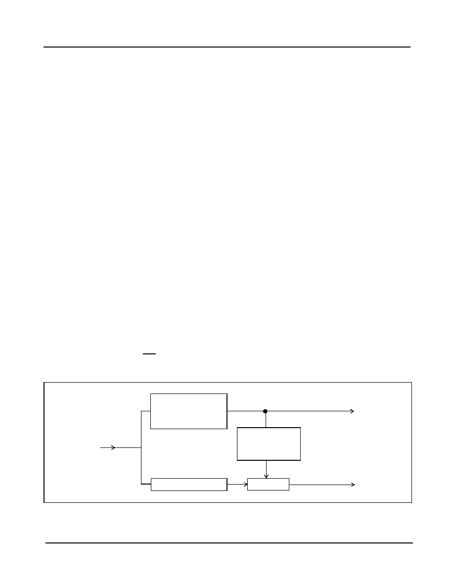
2.4.1 Viterbi Error Count Measurement
A method of estimating the bit error rate at the output of the QPSK block has been provided in the Viterbi decoder.
The incoming data bit stream is delayed and compared with the re-encoded and punctured version of the decoded
bit stream to obtain a count of errors, see Figure 5. The measurement system has a programmable register to
determine the number of data bits (the error count period) over which the count is being recorded. A read register
indicates the error count result and an interrupt can be generated to inform the host microprocessor that a new
count is available.
The VIT_ERRPER_register is programmed with the required number of data bits (the error count period)
(VIT_ERRPER[7:0]). The count of errors found during this period is loaded by the ZL10313 into the
VIT_ERRCNT_H-M-L trio of registers when the bit count VIT_ERRPER[7:0] is reached. At the same time an
interrupt is generated on the IRQ line. Setting the IE_FEC[2] bit in the IE_FEC register enables the interrupt.
Reading the register does not clear VIT_ERRCNT [23:0], it is only loaded with the error count.
Figure 5 - Viterbi Block Diagram
Data Bit Stream
Error Count
Comp
Viterbi
Encoder
Delay
Viterbi
Decoder
ZL10313
Data Sheet
10
Zarlink Semiconductor Inc.
Figure 6 - Viterbi Error Count Measurement
Figure 6 shows the bit errors rising until the maximum programmed value of VIT_ERRPER is reached, when an
interrupt is generated on the IRQ line to advise the host microprocessor that a new value of bit error count has been
loaded into the VIT_ERRCNT [23:0] register. The IRQ line will go high when the IE_FEC register is read by the host
microprocessor. The error count may be expressed as a ratio:
2.4.1.1 Viterbi Error Count Coarse Indication
To assist in the process of aligning the receiver dish aerial, a coarse indication of the number of bit errors being
received can be provided by monitoring the STATUS line with the following set up conditions.
The frequency of the output waveform will be a function of the bit error count (triggering the maximum value
programmed into the VIT_MAXERR[7:0] register and the dish alignment on the satellite. This VIT_MAXERR mode
is enabled by setting the FEC_STAT_EN register bit-0. Figure 7 shows the bit errors rising to the maximum value
programmed and triggering a change of state on the STATUS line.
Error
Count
VIT_ERRCNT[23:0]
VIT_ERRPER
Data Bits
IRQ
0
0
VIT_ERRCNT[23:0]
VIT_ERRPER[7:0] * 262144
ZL10313
Data Sheet
11
Zarlink Semiconductor Inc.
Figure 7 - Viterbi Error Count Coarse Indication
2.4.2 The Frame Alignment Block
The frame alignment algorithm detects a sequence of correctly spaced synchronizing bytes in the Viterbi decoded
bit-stream and arranges the input into blocks of data bytes. Each block consists of 204 bytes for DVB and 147 bytes
for DSS. In the DSS mode, the synchronizing byte is removed from the data stream, so only 146 bytes of a block
are passed to the next stage. The frame alignment block also removes the 180� phase ambiguity not removed by
the Viterbi decoder.
2.4.3 The De-Interleaver Block
2.4.3.1 DVB
Before transmission, the data bytes are interleaved with each other in a cyclic pattern of twelve. This ensures the
bytes are spaced out to avoid the possibility of a noise spike corrupting a group of consecutive message bytes.
Figure 8 below shows conceptually how the convolutional de-interleaving system works. The synchronization byte
is always loaded into the First-In-First-Out (FIFO) memory in branch 0. The switch is operated at regular byte
intervals to insert successively received bytes into successive branches. After 12 bytes have been received,
byte 13 is written next to the synchronization byte in branch 0, etc. In the ZL10313, this de-interleaving function is
realized using on-chip Random Access Memory (RAM).
VIT_MAXERR[3:0]
Data Bits
Status
VITERBI
Coarse
Bit
Error
Count
0
0
ZL10313
Data Sheet
12
Zarlink Semiconductor Inc.
Figure 8 - DVB Conceptual Diagram of the Convolutional De-Interleaver Block
2.4.3.2 DSS
Before transmission, the data bytes are interleaved with each other in a cyclic pattern of thirteen. This ensures the
bytes are spaced out to avoid the possibility of a noise spike corrupting a group of consecutive message bytes.
Figure 9 below shows conceptually how the convolutional de-interleaving system works. On the ZL10313, this
function is realized in the same Random Access Memory (RAM) as used for DVB, but utilizing a different
addressing algorithm.
Figure 9 - DSS Conceptual Diagram of the Convolutional De-Interleaver Block
Sync word route
17x11 bytes
17x10 bytes
17x9 bytes
17x8 bytes
17x7 bytes
17x6 bytes
17x5 bytes
17x4 bytes
17x3 bytes
17x2 bytes
17x1
0
1
2
3
4
5
6
7
8
9
10
11
0
1
2
3
4
5
6
7
8
9
10
11
One
byte per
position
1
0
145
Output
2
Input
12D
12D
12D

ZL10313
Data Sheet
13
Zarlink Semiconductor Inc.
2.4.4 The Reed-Solomon Decoder Block
DVB and DSS data are encoded using shortened versions of the Reed-Solomon code of block length 255,
containing 239 message bytes and 16 check bytes, that is (255,239) with T = 8. Both encoders use the same
generator polynomial. The code block size for DVB is 204 and that for DSS is 146. Hence DVB code is (204, 188)
and DSS code is (146, 130), with both having T = 8. The block structure of the DVB and DSS Reed-Solomon codes
are as shown in Figure 10 and Figure 11 below.
The Reed-Solomon decoder can correct up to eight byte errors per packet. If there are more than eight bytes
containing errors, the packet is flagged as uncorrectable using the BKERR pin 63. In the case of DVB the Transport
Error Indicator (TEI) bit of the MPEG packet is set to 1, if setting of TEI is enabled.
Figure 10 - DVB Block Structure
Figure 11 - DVB Energy Dispersal Conceptual Diagram
Sync byte
187 bytes
16 check bytes
Reed-Solomon encoded block
Sync byte
187 bytes
MPEG transport packet
130 bytes
16 check bytes
Reed-Solomon encoded block
130 bytes
DSS transport packet

ZL10313
Data Sheet
14
Zarlink Semiconductor Inc.
2.4.5 The Energy Dispersal (de-scrambler) Block, DVB Only
Before Reed-Solomon encoding in the DVB transmission system, the MPEG2 data stream is randomised using the
configuration shown in Figure 12 below. This is a Pseudo Random Binary Sequence (PRBS) generator, with the
polynomial:
1 + X
14
+ X
15
The PRBS registers are loaded with the initialisation sequence as shown, at the start of the first transport packet in
a group of eight packets. This point is indicated by the inverted sync byte 0xB8 (the normal DVB sync byte is 0x47).
The data starting with the first byte after the sync byte are randomised by exclusive-ORing data bits with the PRBS
(the sync bytes themselves are not randomised). In the decoder, the process of de-randomising or de-scrambling
the data is exactly the same as described above. The de-scrambler also inverts the sync byte 0xB8 so that all
MPEG output packets have the same sync byte 0x47.
Figure 12 - DVB Energy Dispersal Conceptual Diagram
2.4.6 Output Stage
The transport stream can be output in a byte-parallel or bit-serial mode. The output interface consists of an 8-bit
output, output clock, a packet validation level, a packet start pulse and a block error indicator.
The output clock rate depends on the symbol rate, QPSK/BPSK choice, convolutional (Viterbi) coding rate,
DVB/DSS choice and byte-parallel or bit-serial output mode. This rate is computed by ZL10313 to be very close to
the minimum required to output packet data without packet overlap. Furthermore, the packets at the output of
ZL10313 are as evenly spaced as possible to minimize packet position movement in the transport layer. The
maximum movement in the packet synchronization byte position is limited to �1 output clock period.
2.5 Control
Automatic symbol rate search, code rate search, signal acquisition and signal tracking algorithms are built into the
ZL10313 using a sophisticated on-chip controller. The software interaction with the device is via a simple Command
Driven Control (CDC) interface. This CDC maps high level inputs such as symbol rates in MSps and frequencies in
MHz, to low level on-chip register settings. The on-chip control state machine and the CDC significantly reduces the
software overhead as well as the channel search times. There is also an option for the host processor to by-pass
both the CDC as well as the on-chip controller and take direct control of the QPSK demodulator. Once the ZL10313
has locked to the signal, any frequency offset can be read from the LNB_FREQ error registers 7 and 8. The
frequency synthesiser under the software control can be re-tuned in frequency to optimise the received signal
within the baseband filter bandwidth. Note that ZL10313 compensates for any frequency offsets before QPSK
1
2
3
4
5
6
7
8
9
10
11
12
13
14
15
1
0
0
0
0
0
0
0
0
0
0
0
1
1
1
XOR
Initialisation sequence
ZL10313
Data Sheet
15
Zarlink Semiconductor Inc.
demodulation. Hence a frequency offset will not necessarily lead to a performance loss. Performance loss will occur
only if a significant part of the signal is cut off by the base-band filter, due to this frequency offset. This will happen
only if the symbol rate is close to the maximum supported by that filter. In such an event it is recommended that
front-end be re-tuned to neutralise this error before the filter. It is then necessary for the ZL10313 to re-acquire the
signal.
The ZL10313 can generate control signals to enable full control of the dish and LNB. The chip implements the
signals needed for the full DiSEqC specification. This includes high/low band selection, polarization and dish
position. In this mode, the symbol rate in MSps and Viterbi code rate are the only values needed to start the
ZL10313 searching for the signal. The CDC module maps the high level parameters into the various low level
register settings needed to acquire and track the signal. The low level registers may be read and directly modified
to suit very specific requirements. However, this is not recommended.
Figure 13 - ZL10313 Control Structure
2.5.1 Symbol Rate and Code Rate Search Mode
Where the symbol rate and/or the Viterbi code rate are unknown, the ZL10313 can be programmed to search for
QPSK/BPSK signals. The user should define the range(s) over which the search is required. The ZL10313 will then
locate and track any signal detected. Failure to find a QPSK signal in the specified frequency and specified symbol
rate ranges will be indicated by interrupts. ZL10313 will carry on searching these ranges after issuing these
interrupts. When the ZL10313 has locked onto a signal, the symbol rate in MSps may be read from the MONITOR
registers. The Viterbi code rate may be read from the FEC_STATUS register. This search facility is primarily for use
during the initial installation of a receiver.
2.6 DiSEqC Transmit and Receive Messages
The ZL10313 has the capability to send and receive DiSEqC messages. Eight registers are provided to store a
message for transmission and a further eight registers are provided to store a received message. The received
bytes have a parity bit and a parity error bit in addition to the eight data bits. These additional bits are read out in
sequence following the data bits, so two byte reads are required for each data byte.
2.6.1 DiSEqC Transmitting Messages
The sequence of events to send a message are as follows:
1. Load the required message bytes into the DiSEqC instruction register. Sequential writes to the same register are
achieved by setting the Inhibit Auto Incrementing (IAI) bit 7 in RADD, the register address byte.
2. Load the number of bytes (less one) in the DiSEqC instruction in the register DiS_Mode[5:3].
Command
Driven
Control
ZL10313
format
registers
Acquisition/
Track
State Machine
QPSK
Low level register read/write
High level input/output
(MSps, MHz)

ZL10313
Data Sheet
16
Zarlink Semiconductor Inc.
3. Set DiS_Mode[2:0] = 4 to command the ZL10313 to encode the data and transmit the message.
4. Reset DiS_Mode[2:0] to either 0 or 1 depending on previous setting of 22 kHz off or on. The data loaded into the
DiSEqC_INSTR register is retained, so that if the same message is to be repeated, stage 1 above can be omit-
ted.
2.6.2 DiSEqC Receiving Messages
The ZL10313 will automatically listen for DiSEqC messages 5 ms after a message has been transmitted. If a return
message is expected, the DiS_Mode[2:0] must be set to zero in order to leave the LNB control signal free for
another DiSEqC transmitter to respond. The sequence of events to receive a message are as follows:
1. Ensure that DiSEqC2/GPP2 pin 2 is an input by setting GPP_CTRL register address-20 bit-5 to zero.
2. Enable interrupts if the IRQ pin 43 is used to interrupt the host processor in DiSEqC2_CTRL1 register 121.
3. Monitor DiS_INT register.
4. If bit-3 = 1 and bit-1 = 0, there has been no message received.
5. If a message has been received, bit-0 will be set. If bit-1 is also set the message is complete. DiS_INT register
bits-7-4 indicate how many bytes have been received.
6. Read the received message from DiS_FIFO register 120 by setting the Inhibit Auto Incrementing (IAI) bit-7 in
RADD, the register address byte and sequentially reading DiS_FIFO for the indicated number of bytes. Each
data byte read requires two 2-wire bus reads. The second or the pair of bytes contains the parity bit and a parity
bit error indicator.
The user may choose to wait for the end of message indication, before reading the message, if it is known that the
message is not greater than eight bytes. However, if the length of message is not known, the message should be
read out of the FIFO by the host as it is being received. Care must be taken to avoid a FIFO buffer overflow.
DiS_INT register bits-7-4 will indicate how many bytes remain in the FIFO.
3.0 Microprocessor Control
3.1 RADD: 2-wire Register Address (W)
RADD is the internal 2-wire bus register address. It is the first byte written after the ZL10313 2-wire bus address
when in write mode.
To write to the chip, the bus master should send a START condition and the chip address with the write bit set,
followed by the register address where subsequent data bytes are to be written. Finally, when the 'message' has
been sent, a STOP condition is sent to free the bus.
To read from the chip from register address zero, the bus master should send a START condition and the chip
address with the read bit set, followed by the requisite number of clocks to read the bytes out. Finally a STOP
condition is sent to free the bus. RADD is not sent in this case.
To read from the chip from an address other than zero, the bus master should send the chip address with the write
bit set, followed by the register address from where subsequent data bytes are to be read. Then the bus master
should send a repeat START condition and the chip address with the read bit set, followed by the requisite number
of CLK1 clocks to read the required bytes out. Finally a STOP condition is sent to free the bus. A STOP condition
resets the RADD value to 00.

ZL10313
Data Sheet
17
Zarlink Semiconductor Inc.
RADD (virtual register, address none)
bit-7:
IAI
High = Inhibit auto increment
Low = Increment addresses
bits 6-0:
AD[6:0]
register address, numbers in the range 0 to 127 are allowed
When the register address is incremented to 127 it stops and the bus will continue to write to or read from register
127 until a STOP condition is sent.
3.2 Primary 2-wire Bus Interface
The primary 2-wire bus serial interface uses pins:
DATA1 (pin 11) serial data, the most significant bit is sent first.
CLK1 (pin 10) serial clock.
The 2-wire bus address is determined by applying Vdd or Gnd to the ADDR[4:1] pins while the three MSBs of the
address are internally set to `0'.
For compatibility with earlier devices, the 2-wire bus address will normally be 0001 110 R/W and the pins connected
as follows:
When the ZL10313 is powered up, the Reset pin 1 should be maintained low for typically 100 ms after Vdd and
CVdd have reached normal operation levels, and the Sleep pin 9 has gone low. This is to ensure that the crystal
oscillator and internal PLL have become fully established and that the internal reset signal is fully clocked into all
parts of the circuit. As the reset pin is pulled high, the logic levels on Addr[4:1] are latched to become the 2-wire bus
address AD[6:0].
The circuit works as a slave transmitter with the eighth bit set high or as a slave receiver with the eighth bit set low.
In receive mode, the first data byte is written to the RADD virtual register, which forms the register sub-address.
Bit 7 of the RADD register, IAI is an Inhibit Auto Increment function. When the IAI bit is set high, the automatic
incrementing of register addresses is inhibited. IAI set low is the normal situation so that data bytes sent on the
2-wire bus after the RADD register data are loaded into successive registers. This automatic incrementing feature
avoids the need to individually address each register.
Following a valid chip address, the 2-wire bus STOP command resets the RADD register to 00. If the chip address
is not recognised, the ZL10313 will ignore all activity until a valid chip address is received. The 2-wire bus START
command does NOT reset the RADD register to 00. This allows a combined 2-wire bus message to point to a
particular read register with a write command, followed immediately with a read data command. If required, this
could next be followed with a write command to continue from the latest address. Finally a STOP command should
be sent to free the bus.
When the 2-wire bus is addressed (after a recognised STOP command) with the read bit set, the first byte read out
will be the content of register 00.
NAME
ADR
bit-7
bit-6
bit-5
bit-4
bit-3
bit-2
bit-1
bit-0
Def
hex
RADD
N/A IAI
AD6
AD5
AD4
AD3
AD2
AD1
AD0
W
-
Addr[4]
Addr[3]
Addr[2]
Addr[1]
Vdd
Vdd
Vdd
Gnd
ZL10313
Data Sheet
18
Zarlink Semiconductor Inc.
3.3 Secondary 2-wire Bus for Tuner Control
The ZL10313 has a General Purpose Port that can be configured to provide a secondary 2-wire bus with full bi-
directional operation. When pass-through is enabled, a transparent connection is made to the tuner. This innovative
design simplifies the software required to program the tuner.
Pass-through mode is selected by setting register (20) GPP_CTRL[bit-6] = 1.
The allocation of the pins is: DATA2 = pin14, CLK2 = pin 15.
4.0 Electrical Characteristics
4.1 Recommended Operating Conditions
4.2 Absolute Maximum Ratings
Note 1: Stresses exceeding these listed under 'Absolute Ratings' may induce failure. Exposure to absolute maximum ratings for
extended periods may reduce reliability. Functionality at or above these conditions is not implied.
Parameter
Symbol
Min.
Typ.
Max.
Units
Core power supply voltage
CVdd
1.71
1.8
1.89
V
Periphery power supply voltage
Vdd
3.13
3.3
3.47
V
Input clock frequency (note
1
&
2
)
1. When not using a crystal, XTI may be driven from an external source over the frequency range shown.
2. The upper limit is set by DiSEqC requirements. If DiSEqC is not required, then external frequencies up to 27.00 MHz can be
used.
Fxt1
3.99
22.66
MHz
Crystal oscillator frequency
Fxt2
9.99
16.01
MHz
CLK1 clock frequency
3
(with 10 MHz or above)
3. The maximum serial clock speed on the primary 2-wire bus is related to the input clock frequency and is limited to 100 kHz with
a 4.0 MHz clock.
Fclk1
400
kHz
Ambient operating temperature
0
70
�C
Parameter
Symbol
Min.
Max.
Unit
Power supply
Vdd
-0.3
4.5
V
CVdd
-0.3
2.3
Voltage on input pins (5 V rated)
Vi
-0.3
6.5
V
Voltage on input pins (3.3 V rated)
Vi
-0.3
Vdd + 0.5
V
Voltage on input pins (1.8 V rated, e.g., XTI) Vi
-0.3
CVdd
+
0.5
V
Voltage on output pins (5 V rated)
Vo
-0.3
5.5
V
Voltage on output pins (3.3 V rated)
Vo
-0.3
Vdd + 0.5
V
Voltage on output pins (1.8 V rated, e.g., XTO)
Vo
-0.3
CVdd + 0.5
V
Storage temperature
Tstg
-55
150
�C
Operating ambient temperature
Top
0
70
�C
Junction temperature
Tj
125
�C
ESD protection (human body model)
2
kV

ZL10313
Data Sheet
19
Zarlink Semiconductor Inc.
4.3 Primary 2-Wire Bus Timing
Figure 14 - Primary 2-Wire Bus Timing
Where: S = Start
Sr = Restart, i.e., Start without stopping first.
P = Stop
Parameter: Primary 2-wire bus only
Symbol
Value
Unit
Min.
Max.
CLK1 clock frequency (for XTI
10MHz) f
CLK
0
400
kHz
Bus free time between a STOP and START condition
t
BUF
1300
ns
Hold time (repeated) START condition
t
HD;STA
600
ns
LOW period of CLK1 clock
t
LOW
1300
ns
HIGH period of CLK1 clock
t
HIGH
600
ns
Set-up time for a repeated START condition
t
SU;STA
600
ns
Data hold time (when input)
t
HD;DAT
0
ns
Data set-up time
t
SU;DAT
100
ns
Rise time of both CLK1 and DATA1 signals
t
R
20+0.1Cb
1
1. Cb = the total capacitance on either clock or data line in pF.
300
2
2. The rise time depends on the external bus pull up resistor and bus capacitance.
ns
Fall time of both CLK1 and DATA1 signals, (100pF to ground)
t
F
20+0.1Cb
1
300
ns
Set-up time for a STOP condition
t
SU;STO
600
ns
Table 1 - Primary 2-wire bus timing
ZL10313
Data Sheet
20
Zarlink Semiconductor Inc.
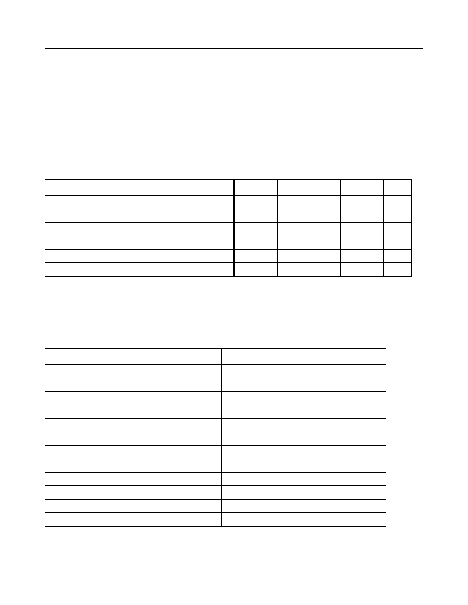
4.4 Crystal Specification
Parallel resonant fundamental frequency (preferred) 9.99 to 16.01 MHz.
Tolerance over operating temperature range �25 ppm.
Tolerance overall �50 ppm.
Nominal load capacitance 30 pF.
Equivalent series resistance <75
Figure 15 - Crystal Oscillator Circuit
Note: The crystal frequency should be chosen to ensure that the system clock would marginally exceed the
maximum symbol rate required, e.g. 10.111 MHz with a multiplier of x9 will give a 91 MHz system clock to
guarantee 45 MSps operation.
4.5 Electrical Characteristics
Conditions (unless specified otherwise):Tamb = 25�C
CVdd = 1.8 V
Vdd = 3.3 V
DC Electrical Characteristics
Parameter
Conditions/Pin
Symbol
Min.
Typ.
Max.
Unit
Core voltage
CVdd
1.71
1.8
1.89
V
Peripheral voltage
Vdd
3.13
3.3
3.47
V
Core current
45 MSps CR 7/8 91 MHz system clock
CIdd
165
mA
Peripheral current
Idd
7
mA
Total power
(91 MHz system
clock)
Ptot1
320
mW
Total power (stand-
by)
ADCs powered down. MPEG outputs
tri-stated
Ptot2
1
2.2
mW
Total power (sleep)
Pin 9 = logic `1' ADCs powered down
Ptot3
1
0.35
mW
Output low level
2, 6 or 12 mA per output (see section
4.6, ZL10313 Pinout Description)
Vol
0.4
V
Output high level
2, 6 or 12 mA per output
Voh
2.4
V
Output leakage
Tri-state when off or open-drain when
high
�1
�A

ZL10313
Data Sheet
21
Zarlink Semiconductor Inc.
Output capacitance
All outputs except XTO, CLK1 & open-
drain types. Excludes packaging
contribution (~0.35 pF)
2.7
pF
Open-drain outputs.
Excludes packaging
contribution (~0.35 pF)
3.3
pF
Input low level
Vil
0.8
V
Input high level
Vih
2.0
V
Input leakage
Vin = 0 or Vdd
�1
�A
Input capacitance
Excludes packaging contribution
(~0.35 pF)
1.5
pF
1. For minimum power, MPEG outputs should be tristated and ADCs powered down.
AC Electrical Characteristics
Parameter
Conditions/Pin
Min.
Typ.
Max.
Unit
ADC Full-scale input single range
(single-ended or differential)
Differential source is
recommended
0.5
1.0
Vpp
ADC analog input resistance
Per input pin
10
k
ADC analog input capacitance
Per input pin
2
pF
ADC input common mode voltage level
0.7
1.7
V
System clock frequency
30.00
100
MHz
Input clock frequency (note
1
and
2
)
1. When not using a crystal, XTI may be driven from an external source over the frequency range shown.
2. The upper limit is set by DiSEqC requirements. If DiSEqC is not required, then external frequencies up to 27.00 MHz can be used.
3.99
22.66
MHz
Crystal oscillator frequency
See Section 4.4 for details
9.99
16.01
MHz
CLK1 clock frequency
3
(with 10 MHz xtal or above)
3. The maximum serial clock speed on the primary 2-wire bus is related to the input clock frequency and is limited to 100 kHz with a
4.0 MHz clock.
400
kHz
MPEG clock input frequency
On either pin #2 or pin #43
note
4
4. Must be calculated from the data input rate.
65
5
5. Also subject to system clock limitations.
MHz
DC Electrical Characteristics (continued)
Parameter
Conditions/Pin
Symbol
Min.
Typ.
Max.
Unit

ZL10313
Data Sheet
22
Zarlink Semiconductor Inc.
4.6 ZL10313 Pinout Description
Pin Description Table
Pin
Name
Description
I/O
Note
V
mA
1
Reset
Active low reset input
I
CMOS
1
5
2
DiSEqC[2]
DiSEqC input for level 2 control. Also usable as
GPP2 (general purpose port pin) for other purposes,
and as MICLK - external clock input for MPEG data.
I/O Open
drain
1
5
6
3
DiSEqC[1]
Horizontal/vertical LNB control (acts as input only in
production test modes)
I/O CMOS
3.3
2
4
DiSEqC[0]
22 kHz output to LNB (acts as input only in
production test modes)
I/O CMOS
3.3
2
9
Sleep
Stops oscillator and sets minimum power levels to
entire device (except ADCs - register controlled
power-down)
I
CMOS
3.3
10
CLK1
Primary 2-wire serial bus clock
I
CMOS
1
5
11
DATA1
Primary 2-wire serial bus data
I/O
Open
drain
1
5
6
14
DATA2
Secondary 2-wire bus data to tuner front end. Also
usable as GPP1 (general purpose port pin) for other
purposes.
I/O Open
drain
1
5
6
15
CLK2
Secondary 2-wire bus clock to tuner front end. Also
usable as GPP0 (general purpose port pin) for other
purposes.
I/O Open
drain
1
5
6
16
OscMode
Controls oscillator mode to suit crystal or external
signal
I CMOS
3.3
19
XTI
Crystal input or external reference clock input
I
CMOS
1.8
20
XTO
Crystal output, includes internal feedback resistor to
XTI
I/O
CMOS
1.8
24
Iin
I channel input
I
analog
25
Iin
I channel negative input
I
analog
29
Qin
Q channel negative input
I
analog
30
Qin
Q channel input
I
analog
35,36,37
38
ADDR[1:4]
Primary 2-wire bus address defining pins
I
CMOS
3.3
41
AGC
AGC sigma-delta output (acts as input only in
production test modes)
I/O
Open
drain
1
5
6
42
Test
For normal operation, this pin must be held at 0 V.
I
CMOS
3.3
43
IRQ
Active low interrupt output. Reading all active
interrupt registers resets this pin. Can also be defined
as MICLK - external clock input for MPEG data
I/O
Open
drain
1
5
6
46
MOSTRT
MPEG output start signal. High during the first byte of
a packet.
O
CMOS
Tri-state
3.3
2
ZL10313
Data Sheet
23
Zarlink Semiconductor Inc.
Note 1: 5 V tolerant pins with thresholds related to 3.3 V.
47
MOVAL
MPEG data output valid. High during the MOCLK
cycles when valid data bytes are being output.
O
CMOS
Tri-state
3.3 2
48,49,52
,53,56,
57,60,61
MDO[0:7]
MPEG transport packet data output bus. Can be tri-
stated under control of a register bit.
O
CMOS
Tri-state
3.3
2
62
MOCLK
MPEG clock output at the data byte rate.
O
CMOS
Tri-state
3.3
12
63
BKERR
Active low uncorrectable block indicator or no-signal
indicator. Mode selected by ERR_IND bit (#7) of the
MON_CTRL register. Can also be inverted.
O
CMOS
Tri-state
3.3
2
64
STATUS
Status output. Register defined function including
audio frequency proportional to BER (acts as input
only in production test modes)
I/O CMOS
3.3
2
5, 39, 55
Vdd
Peripheral supply pins. All pins must be connected.
3.3
27
Vdd
Peripheral supply pin used for the ADC.
3.3
7, 12,
44, 50,
59
CVdd
Core supply pins. All pins must be connected.
1.8
17, 22,
32, 34
CVdd
PLL/ADC supply pins. All pins must be connected.
1.8
6, 8, 13,
40, 45
51, 54,
58
Gnd
Ground supply pins. All pins must be connected.
0
18, 21,
23 26,
28, 31,
33
Gnd
PLL/ADC ground supply pins. All pins must be
connected.
0
Pin Description Table
Pin
Name
Description
I/O
Note
V
mA

ZL10313
Data Sheet
24
Zarlink Semiconductor Inc.
4.7 Alphabetical Listing of Pin-Out
5.0 References
1. European Digital Video Broadcast Standard, ETS 300 421 (A1) Version 1.1.2 - 1997-08.
ETS Secretariat
06921 Sophia Antipolis Cedex
France.
2. Digital Satellite Equipment Control (DiSEqC)
DiSEqCTM Bus Specification Version 4.2 (February 25, 1998)
EUTELSAT
European Telecommunications Satellite Organisation
70, rue Balard - 75502 PARIS Cedex 15
France.
6.0 Trademarks
DiSEqCTM is a trademark of EUTELSAT.
Name
No.
Name
No.
Name
No.
Name
No.
Addr[1]
35
CVdd
59
Gnd
40
MOCLK
62
Addr[2]
36
DATA1
11
Gnd
45
MOSTRT
46
Addr[3]
37
DATA2
14
Gnd
51
MOVAL
47
Addr[4]
38
DiSEqC[0]
4
Gnd
54
OscMode
16
AGC
41
DiSEqC[1]
3
Gnd
58
Qin
29
BKERR
63
DiSEqC[2]
2
Iin
24
Qin
30
CLK1
10
Gnd
6
Iin
25
Reset
1
CLK2
15
Gnd
8
IRQ
43
Sleep
9
CVdd
7
Gnd
13
MDO[0]
48
Status
64
CVdd
12
Gnd
18
MDO[1]
49
Test
42
CVdd
17
Gnd
21
MDO[2]
52
Vdd
5
CVdd
22
Gnd
23
MDO[3]
53
Vdd
27
CVdd
32
Gnd
26
MDO[4]
56
Vdd
39
CVdd
34
Gnd
28
MDO[5]
57
Vdd
55
CVdd
44
Gnd
31
MDO[6]
60
XTI
19
CVdd
50
Gnd
33
MDO[7]
61
XTO
20

www.zarlink.com
Information relating to products and services furnished herein by Zarlink Semiconductor Inc. or its subsidiaries (collectively "Zarlink") is believed to be reliable.
However, Zarlink assumes no liability for errors that may appear in this publication, or for liability otherwise arising from the application or use of any such
information, product or service or for any infringement of patents or other intellectual property rights owned by third parties which may result from such application or
use. Neither the supply of such information or purchase of product or service conveys any license, either express or implied, under patents or other intellectual
property rights owned by Zarlink or licensed from third parties by Zarlink, whatsoever. Purchasers of products are also hereby notified that the use of product in
certain ways or in combination with Zarlink, or non-Zarlink furnished goods or services may infringe patents or other intellectual property rights owned by Zarlink.
This publication is issued to provide information only and (unless agreed by Zarlink in writing) may not be used, applied or reproduced for any purpose nor form part
of any order or contract nor to be regarded as a representation relating to the products or services concerned. The products, their specifications, services and other
information appearing in this publication are subject to change by Zarlink without notice. No warranty or guarantee express or implied is made regarding the
capability, performance or suitability of any product or service. Information concerning possible methods of use is provided as a guide only and does not constitute
any guarantee that such methods of use will be satisfactory in a specific piece of equipment. It is the user's responsibility to fully determine the performance and
suitability of any equipment using such information and to ensure that any publication or data used is up to date and has not been superseded. Manufacturing does
not necessarily include testing of all functions or parameters. These products are not suitable for use in any medical products whose failure to perform may result in
significant injury or death to the user. All products and materials are sold and services provided subject to Zarlink's conditions of sale which are available on request.
Purchase of Zarlink's I
2
C components conveys a licence under the Philips I
2
C Patent rights to use these components in and I
2
C System, provided that the system
conforms to the I
2
C Standard Specification as defined by Philips.
Zarlink, ZL and the Zarlink Semiconductor logo are trademarks of Zarlink Semiconductor Inc.
Copyright Zarlink Semiconductor Inc. All Rights Reserved.
TECHNICAL DOCUMENTATION - NOT FOR RESALE
For more information about all Zarlink products
visit our Web Site at