1
Zarlink Semiconductor Inc.
Zarlink, ZL and the Zarlink Semiconductor logo are trademarks of Zarlink Semiconductor Inc.
Copyright 2005, Zarlink Semiconductor Inc. All Rights Reserved.
Features
� Compliant with ETSI 300 744 DVB-T, Unified
Nordig and DTG performance specifications
� High performance with fast fully blind acquisition
and tracking capability
� Low power consumption: less than 0.32 W, and
eco-friendly standby and sleep modes
� Digital filtering of adjacent channels
� Single 8 MHz SAW filter for 6, 7 & 8 MHz OFDM
� Superior single frequency network performance
� Fast AGC to track out signal fades
� Good Doppler tracking capability
� Enhanced frequency capture range to include
triple offsets
� External 4 MHz clock or single low-cost
20.48 MHz crystal, tolerance up to +/-200 ppm
� Automatic mode (2K/8K), guard and spectral
inversion detection
� Very low driver software overhead due to on-chip
state-machine control
� Novel RF level detect facility via a separate ADC
� Pre and post Viterbi-decoder bit error rates, and
uncorrectable block count
Applications
� Digital terrestrial set-top boxes
� Integrated digital televisions
� Personal video recorders
� PC-TV receivers
� Portable applications
Description
The ZL10353 is a superior fourth generation fully
compliant ETSI ETS300 744 COFDM demodulator that
exceeds, with margin, the performance requirements
of all known DVB-T digital terrestrial television
standards, including Unified Nordig and DTG.
June 2005
Ordering Information
ZL10353QCG
64 Pin LQFP
Trays, Bake & Drypack
ZL10353QCG1 64 Pin LQFP* Trays, Bake & Drypack
ZL10353QCF
64 Pin LQFP
Tape & Reel, Bake & Drypack
ZL10353QCF1
64 Pin LQFP* Tape & Reel,Bake & Drypack
*Pb Free Matte Tin
-10
�
C to +80
�
C
ZL10353
Fully Compliant NorDig Unified COFDM
Digital Terrestrial TV (DTV) Demodulator
Data Sheet
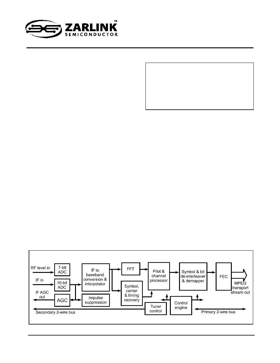
Figure 1 - Block Diagram

ZL10353
Data Sheet
2
Zarlink Semiconductor Inc.
A high performance 10 bit on-chip ADC is used to sample the 44 or 36 MHz IF analogue signal. Advanced digital
filtering of the upper and lower channel enables a single 8 MHz channel SAW filter to be used for 6, 7 and 8 MHz
OFDM signal reception. All sampling and other internal clocks are derived from a single 20.48 MHz crystal or a 4
MHz clock input, the tolerance of which may be relaxed as much as 200 ppm.
The ZL10353 has a wide frequency capture range able to automatically compensate for the combined offset
introduced by the tuner xtal and broadcaster triple frequency offsets.
An on-chip state machine controls all acquisition and tracking operations of the ZL10353 as well as controlling the
tuner via a 2-wire bus. Any frequency range can be automatically scanned for digital TV channels. This mechanism
ensures minimal interaction, maximum flexibility and fast acquisition - very low software overhead.
Also included in the design is a 7-bit ADC to detect the RF signal strength and thereby efficiently control the tuner
RF AGC.
Users have access to all the relevant signal quality information, including input signal power level, signal-to-noise
ratio, pre-Viterbi BER, post-Viterbi BER, and the uncorrectable block counts. The error rate monitoring periods are
programmable over a wide range.
The device is packaged in a 10 x 10 mm 64-pin LQFP and is very low power.
ZL10353
Data Sheet
3
Zarlink Semiconductor Inc.
1.0 Pin & Package Details
1.1 Pin Outline
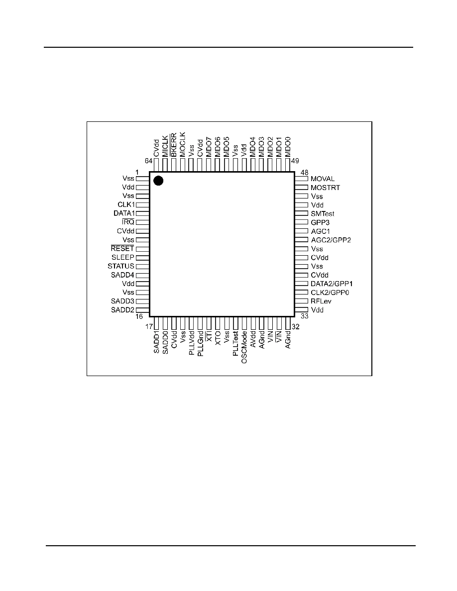
Figure 2 below shows the basic, non-diversity, pin functions of the ZL10353. The device can effectively be set up in
seven different pin configurations, so for brevity only this version is shown.
Figure 2 - Pin Outline

ZL10353
Data Sheet
5
Zarlink Semiconductor Inc.
1.3 Pin Description
CVdd
7
MDO6
57
SADD4/Dv2
12
Vss
25
CVdd
19
MDO7
58
SLEEP
10
Vss
38
CVdd
37
MICLK
63
SMTEST
44
Vss
40
CVdd
39
MOCLK/DvClk
61
STATUS/Dv3/
Dv1
11
Vss
46
CVdd
59
MOSTRT
47
Vdd
2
Vss
55
CVdd
64
MOVAL/DvVal
48
Vdd
13
Vss
60
DATA1
5
OSCMODE
27
Vdd
33
XTI
23
DATA2/GPP1
36
PLLGND
22
Vdd
45
XTO
24
Pin No
Name
Pin Description
I/O
Type
V
mA
MPEG Pins
47
MOSTRT
MPEG packet start
O
CMOS Tristate
3.3
1
48
MOVAL (or DvVal-O)
MPEG/diversity data valid
O
3.3
1
49-53,
56-58
MDO(0:4)/Dv(0:4)-O
MDO(5:7)
MPEG/diversity data bus
O
3.3
1
61
MOCLK (or DvClk-O)
MPEG/diversity clock out
O
3.3
1
62
BKERR
Block error
O
3.3
1
63
MICLK
MPEG clock in
I
CMOS
3.3
11
STATUS (or Dv3/1)
Status output or diversity
data
I/O
3.3
1
6
IRQ (or Dv4/0)
Interrupt output or diversity
data
I/O
Open drain
5
6
Control Pins
4
CLK1
Serial clock
I
CMOS
5
5
DATA1
Serial data
I/O
Open drain
5
6
Function
Pin
Function
Pin
Function
Pin
Function
Pin
Table 2 - Pin Names - Alphabetical Order (continued)