Document Outline
- Features
- Applications
- Description
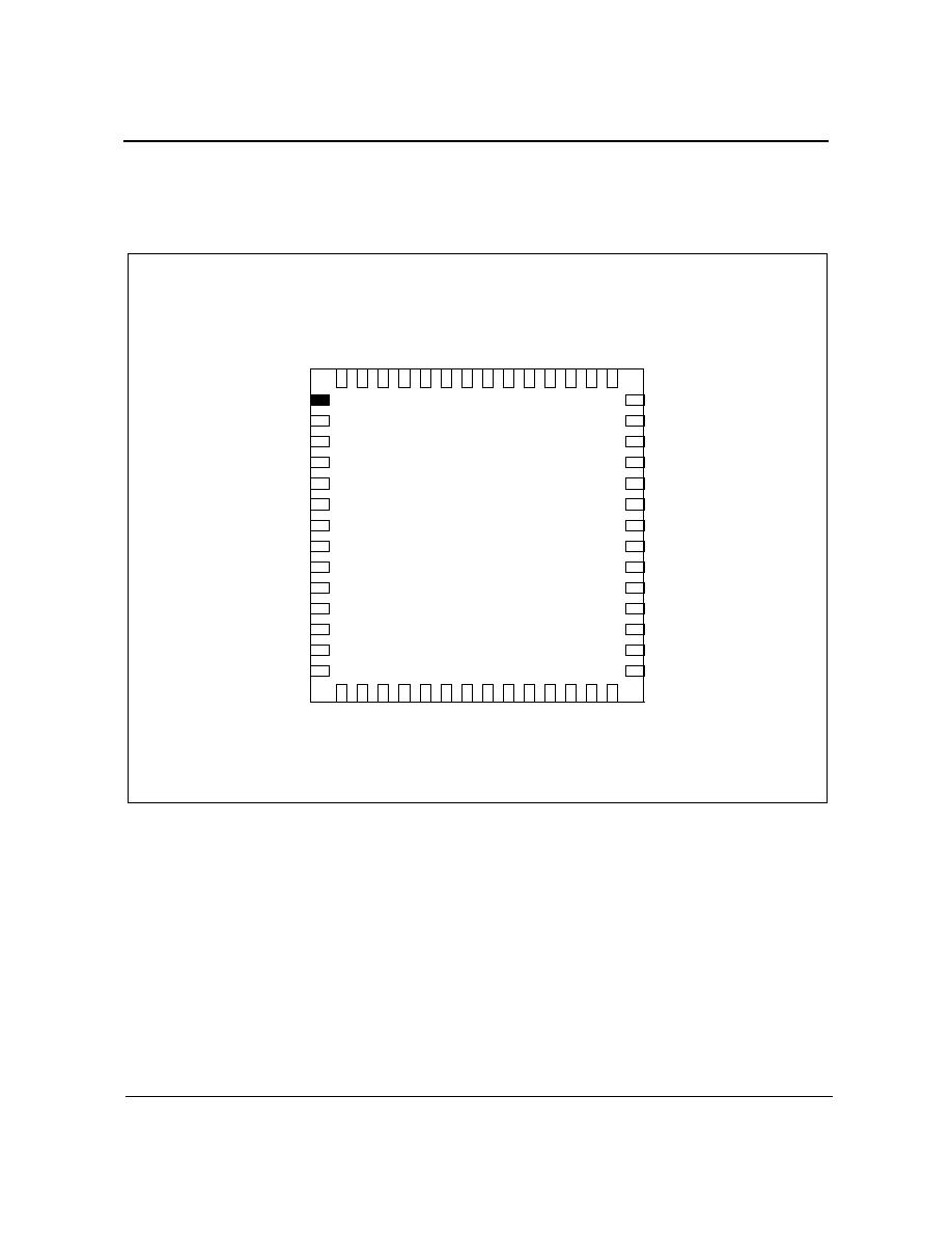
- Package Diagram
- Figure 2 - ZL20200 Package Diagram
- Pin Description
- Pin Description Table�
- Figure 1 - Block Diagram
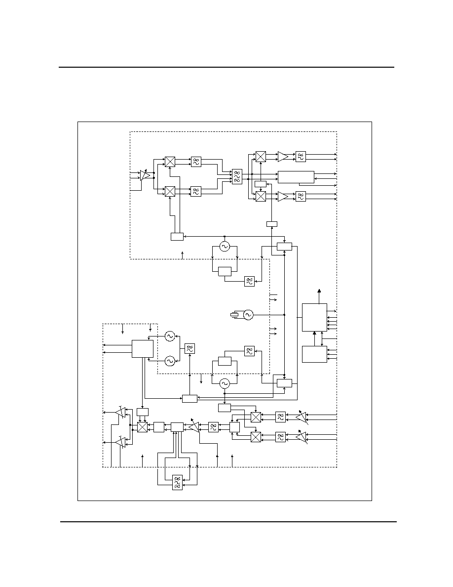
- 1.0 General Description
- Figure 3 - ZL20200 Detailed Block Diagram
- 1.1 Receive Path
- 1.1.1 IS136
- Table 1 - IS136 Receive Gain and Filter Distribution
- Figure 4 - IS136 Receiver Signal Flow
- 1.1.2 AMPS FM
- Table 2 - AMPS FM Receive Gain and Filter Distribution
- Figure 5 - AMPS Receive Signal Flow
- 1.2 Transmit
- Table 3 - Transmit Circuit blocks
- Figure 6 - Transmit Path
- Figure 7 - External Transmit IF Filter
- 1.3 UHF LO and Frequency Doubler
- 1.4 UHF Frequency Synthesizer
- Figure 8 - UHF Synthesizer
- Figure 9 - Count Sequence for UHF PLL with 4 Modulus Prescaler
- Figure 10 - UHF Synthesizer - Fractional N Operation
- 1.5 VHF Frequency Synthesizers
- Figure 11 - VHF Frequency Synthesizer
- 1.6 Internal Clock Generation
- Figure 12 - Typical VCO Tank Circuit
- 1.7 VHF VCO
- 1.8 Power Supply Connections
- Table 4 - Power Supply Connections
- 2.0 Programming and Control
- Figure 13 - Serial Bus Timing
- 2.1 Power Control Registers - Address 0 to 3
- Table 5 - Power Control Registers
- Table 6 - Power Control Register Functions
- 2.1.1 Power Control Modes - TDMA (IS136)
- Table 7 - Programming for the Power Control Registers (0 - 3)�
- 2.1.2 Power Control Modes - AMPS
- Table 8 - Enable Registers
- 2.2 Operating Register Address 4
- Table 9 - Function of the Receive Bits
- Table 10 - Function of the Transmit Bits�
- Table 11 - Gain of the Transmit Output Stage
- Figure 14 - Transmit Output Stage Current versus Gain Control
- Table 12 - VGA Threshold Voltage
- Table 13 - VGA Current Reduction
- Table 14 - Output Stage Current
- Table 15 - Control Register Settings�
- 2.3 Synthesizer Register - Address 5
- 2.3.1 UHF PLL and LO
- Table 16 - UHF PLL and LO Control
- Table 17 - Fractional N Denominator
- 2.3.2 UHF PLL Charge Pump Current
- Table 18 - UHF PLL Charge Pump Current
- 2.3.3 Receive LO Set Up
- Table 19 - Receive LO Set Up
- Table 20 - Receive VHF PLL Charge Pump Current
- 2.3.4 Transmit LO Set Up
- Table 21 - Transmit LO Set Up
- Table 22 - Transmit VHF PLL Charge Pump Current
- 2.4 Control Register - Address 6
- 2.4.1 IS136 Baseband Gain
- 2.4.2 TCXO Reference Selection
- Table 24 - TCXO Reference Selection
- 2.4.3 Discriminator Output Filtering
- Table 25 - FM Discriminator Output Filter Control
- 2.4.4 Transmit Baseband Gain
- Table 26 - Transmit Baseband Gain
- 2.4.5 Mode Control
- 2.5 Register Address 7 - Not Used
- 2.6 Test Mode Register - Address 8
- 2.7 UHF PLL Divider Programming Register - Address 9
- 2.8 UHF PLL Reference Divider and Fractional N Programming Register - Address 10
- 2.9 Receive VHF PLL Divider Programming Register - Address 11
- 2.10 Receive VHF PLL Reference Divider Programming Register - Address 12
- 2.11 Transmit VHF PLL Divider Programming Register - Address 13
- 2.12 Transmit VHF PLL Reference Divider Programming Register Address 14
- 2.13 PLL Lock Detect & Fractional N Compensation Programming Register Address 15
- 2.13.1 Fractional N Compensation
- 2.13.2 PLL Lock detect counters
- 3.0 Absolute Maximum Ratings
- 4.0 Operating Conditions
- Operating Conditions (continued)
- 5.0 Electrical Characteristics
- 6.0 Typical Performance Curves
1
Zarlink Semiconductor Inc.
Zarlink, ZL and the Zarlink Semiconductor logo are trademarks of Zarlink Semiconductor Inc.
Copyright 2003, Zarlink Semiconductor Inc. All Rights Reserved.
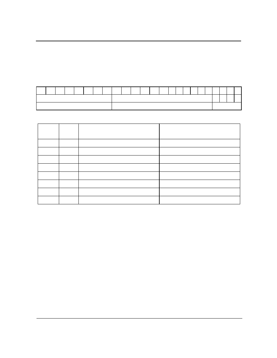
Features
� Dual Band IS136 (800/1900 MHz) Compatible
� Fully Integrated Dual Band Transceiver
� Receive - IF to Baseband I and Q
� Transmit - Baseband I / Q to RF
� Integrated Filters
� FM Demodulator
� RF and IF Synthesizers
� Fully Programmable via serial bus
� 3 Volt operation
� Small scale package
Applications
� Dual Band (850/PCS1900) TDMA/AMPS Mobile
Telephones
� Cellular 850 MHz TDMA/AMPS Mobile
Telephones
� PCS1900 TDMA Mobile Telephones
� Cellular Telematic Systems
Description
The ZL20200 is a fully integrated transceiver for dual
band IS136/AMPS handsets. The IF input to the
receive path is amplified and down-converted to
baseband I and Q signals. Gain control is provided.
Baseband filtering is also included. A FM demodulator
is also provided to support AMPS operation.
The transmit path consists of a quadrature modulator,
gain control at IF and up-conversion to RF. Dual band
RF outputs are provided. The transmit output stages
can be programmed to optimize performance and
current consumption.
ZL20200 also includes a fractional N RF synthesizer
and two IF synthesizers to provide all local oscillator
signals required.
December 2003
Ordering Information
ZL20200/LCE (Tubes)
56pinQFN
ZL20200/LCF (Tape and Reel) 56pinQFN
ZL20200/LDE (Tubes) Stamped 56pinQFN
ZL20200/LDF (Tape and Reel)Stampled 56pinQFN
-40 to +85�C
ZL20200
Dual Band IS136/AMPS Transceiver
Data Sheet
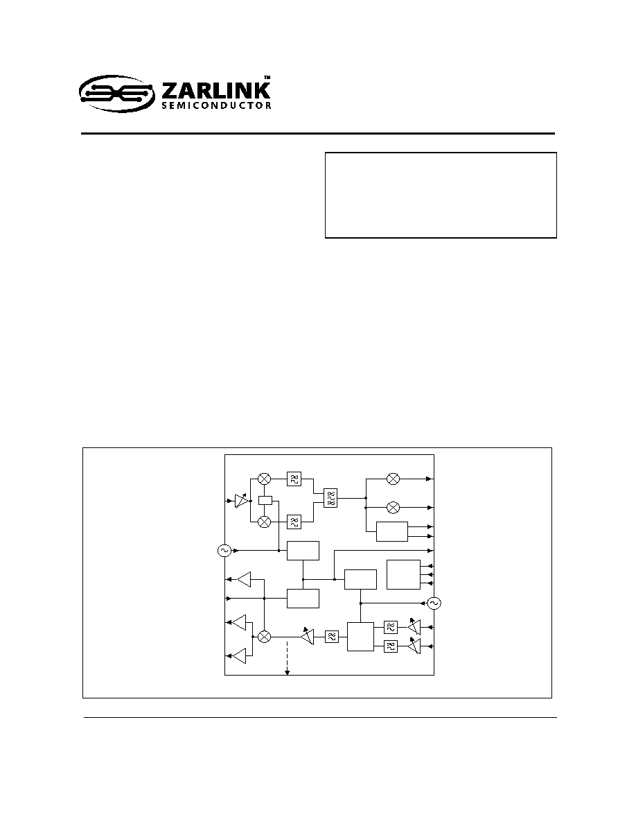
Figure 1 - Block Diagram
Rx VHF
PLL
Serial
Interface
Control
FM
Demod
IQ
Mod
UHF
PLL
Tx VHF
PLL
Rx I
Rx Q
FM
RSSI
Tx I
Tx Q
IS136
UHF VCO
900 MHz Tx
1900 MHz Tx
Tx IF Filter
(Opt)
90�
UHF LO O/P
LOCK DET
ZL20200
Data Sheet
2
Zarlink Semiconductor Inc.
Flexible programming is provided via a 3 wire serial bus. Additional control pins allow accurate timing control when
switching between modes.
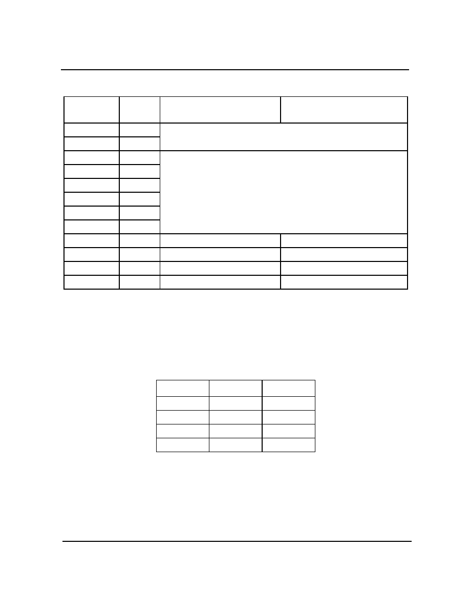
Package Diagram
Figure 2 - ZL20200 Package Diagram
SDAT
SCLK
SLATCH
TCXO
VCC UHF PLL
UHF CP
900 LO OUT
1900 LO OUT
RESETB
ENABLE1
900 LO IN
VCC UHF LO
TX 900
TX DEG900
TX DEG1900
TX 1900
EN
ABLE2
TX FILT IN+
TX FILT IN-
V
CC T
X
TX Q-
TX FILT OUT+
TX FILT OUT-
TX Q+
V
CC CONT
ROL
IF1 IN+
IF1 IN-
NC
NC
RX GAIN
V
CC RX
P
L
L
RX
V
C
O+
FM OU
T
RX I-
RX I+
RX
V
C
O-
RX Q-
RX Q+
RSSI
RX CP
VCC VHF CP
LOCK DET
TX RXB
TX CP
TX I-
TX I+
ISET
VCC TX PLL
TX VCO-
VCC UHF LO OUT
TX VCO+
V
CC TX
RF
1900 LO IN
TX GAIN
V
CC RX
FM FB
ZL20200
ZL20200
Data Sheet
3
Zarlink Semiconductor Inc.
Pin Description
Pin Description Table
No
Pin Name
Type
Description
1
SDAT
Input
Serial Interface - Data
2
SCLK
Input
Serial interface - Clock
3
SLATCH
Input
Serial Interface - Latch
4
TCXO
Input
Reference input from TCXO
5
VCC UHF PLL
Power
Power
6
UHF CP
Output
UHF PLL Charge Pump Output
7
VCC UHF LO OUT Power
Power to LO output stages
8
900 LO OUT
Output
900 MHz buffered LO output to external receiver mixer
9
1900 LO OUT
Output
1900 MHz buffered LO output to external receiver mixer
10
RESETB
Input
Reset (Active low)
11
ENABLE1
Input
Mode Control
12
900 LO IN
Input
900 MHz LO input
13
VCC UHF LO
Power
Power to UHF LO input stage
14
1900 LO IN
Input
1900 MHz LO input
15
VCC TX RF
Power
Power to transmit RF output stages
16
TX 900
Output
900 MHz transmit output
17
TX DEG900
Degeneration for 900 MHz output - Connect to Ground
18
TX DEG1900
Degeneration for 1900 MHz output - Connect to Ground
19
TX 1900
Output
1900 MHz transmit output
20
ENABLE2
Input
Mode Control
21
TX GAIN
Input
Transmit gain control
22
TX FILT IN+
Input
Input from transmit IF filter (optional)
23
TX FILT IN-
Input
24
VCC TX
Power
Power to transmit stages
25
TX FILT OUT+
Output
Output to transmit IF filter (optional)
26
TX FILT OUT-
Output
27
TX Q+
Input
Q transmit signal from baseband
28
TX Q-
Input
29
TX VCO+
Transmit Oscillator tank circuit
30
TX VCO-
31
VCC TX PLL
Power
Power to Transmit VHF PLL
32
TX I+
Input
I transmit signal from baseband
33
TX I-
Input
34
TX RXB
Input
Transmit / Receive control
35
TX CP
Output
Transmit VHF PLL charge pump output
36
LOCK DET
Output
PLL Lock Detect Output
37
ISET
Connect 50 kohm resistor to ground to set internal reference current
ZL20200
Data Sheet
4
Zarlink Semiconductor Inc.
38
VCC VHF CP
Power
Power to VHF charge pump outputs
39
RX CP
Output
Receive VHF PLL charge pump output
40
RSSI
Output
RSSI Output
41
RX Q+
Output
Baseband Q signal
42
RX Q-
Output
43
RX I+
Output
Baseband I signal
44
RX I-
Output
45
FM OUT
Output
Demodulated FM output
46
FM FB
Feedback to FM output stage
47
RX VCO-
Receive second LO Oscillator tank circuit
48
RX VCO+
49
VCC RX PLL
Power
Power to receive VHF PLL
50
VCC RX
Power
Power to receive stages
51
RX GAIN
Input
Receive gain control
52
NC
Not Connected
53
NC
Not Connected
54
IF1 IN-
Input
IF Input (1)
55
IF1 IN+
Input
IS136 Input
56
VCC CONTROL
Power
Power to serial interface logic
Pin Description Table (continued)
No
Pin Name
Type
Description

ZL20200
Data Sheet
5
Zarlink Semiconductor Inc.
Table of Contents
Features . . . . . . . . . . . . . . . . . . . . . . . . . . . . . . . . . . . . . . . . . . . . . . . . . . . . . . . . . . . . . . . . . . . . . . . . . . . . . . . . . 1
Applications . . . . . . . . . . . . . . . . . . . . . . . . . . . . . . . . . . . . . . . . . . . . . . . . . . . . . . . . . . . . . . . . . . . . . . . . . . . . . 1
Description . . . . . . . . . . . . . . . . . . . . . . . . . . . . . . . . . . . . . . . . . . . . . . . . . . . . . . . . . . . . . . . . . . . . . . . . . . . . . . 1
Package Diagram . . . . . . . . . . . . . . . . . . . . . . . . . . . . . . . . . . . . . . . . . . . . . . . . . . . . . . . . . . . . . . . . . . . . . . . . . 2
Pin Description . . . . . . . . . . . . . . . . . . . . . . . . . . . . . . . . . . . . . . . . . . . . . . . . . . . . . . . . . . . . . . . . . . . . . . . . . . . 3
1.0 General Description. . . . . . . . . . . . . . . . . . . . . . . . . . . . . . . . . . . . . . . . . . . . . . . . . . . . . . . . . . . . . . . . . . . . . 8
1.1 Receive Path . . . . . . . . . . . . . . . . . . . . . . . . . . . . . . . . . . . . . . . . . . . . . . . . . . . . . . . . . . . . . . . . . . . . . . . . 9
1.1.1 IS136 . . . . . . . . . . . . . . . . . . . . . . . . . . . . . . . . . . . . . . . . . . . . . . . . . . . . . . . . . . . . . . . . . . . . . . . . . 9
1.1.2 AMPS FM. . . . . . . . . . . . . . . . . . . . . . . . . . . . . . . . . . . . . . . . . . . . . . . . . . . . . . . . . . . . . . . . . . . . . 11
1.2 Transmit. . . . . . . . . . . . . . . . . . . . . . . . . . . . . . . . . . . . . . . . . . . . . . . . . . . . . . . . . . . . . . . . . . . . . . . . . . . 14
1.3 UHF LO and Frequency Doubler. . . . . . . . . . . . . . . . . . . . . . . . . . . . . . . . . . . . . . . . . . . . . . . . . . . . . . . . 16
1.4 UHF Frequency Synthesizer . . . . . . . . . . . . . . . . . . . . . . . . . . . . . . . . . . . . . . . . . . . . . . . . . . . . . . . . . . . 16
1.5 VHF Frequency Synthesizers . . . . . . . . . . . . . . . . . . . . . . . . . . . . . . . . . . . . . . . . . . . . . . . . . . . . . . . . . . 19
1.6 Internal Clock Generation . . . . . . . . . . . . . . . . . . . . . . . . . . . . . . . . . . . . . . . . . . . . . . . . . . . . . . . . . . . . . 20
1.7 VHF VCO. . . . . . . . . . . . . . . . . . . . . . . . . . . . . . . . . . . . . . . . . . . . . . . . . . . . . . . . . . . . . . . . . . . . . . . . . . 20
1.8 Power Supply Connections . . . . . . . . . . . . . . . . . . . . . . . . . . . . . . . . . . . . . . . . . . . . . . . . . . . . . . . . . . . . 21
2.0 Programming and Control . . . . . . . . . . . . . . . . . . . . . . . . . . . . . . . . . . . . . . . . . . . . . . . . . . . . . . . . . . . . . . 22
2.1 Power Control Registers - Address 0 to 3 . . . . . . . . . . . . . . . . . . . . . . . . . . . . . . . . . . . . . . . . . . . . . . . . . 22
2.1.1 Power Control Modes - TDMA (IS136) . . . . . . . . . . . . . . . . . . . . . . . . . . . . . . . . . . . . . . . . . . . . . . 24
2.1.2 Power Control Modes - AMPS . . . . . . . . . . . . . . . . . . . . . . . . . . . . . . . . . . . . . . . . . . . . . . . . . . . . . 26
2.2 Operating Register Address 4 . . . . . . . . . . . . . . . . . . . . . . . . . . . . . . . . . . . . . . . . . . . . . . . . . . . . . . . . . . 27
2.3 Synthesizer Register - Address 5 . . . . . . . . . . . . . . . . . . . . . . . . . . . . . . . . . . . . . . . . . . . . . . . . . . . . . . . 31
2.3.1 UHF PLL and LO . . . . . . . . . . . . . . . . . . . . . . . . . . . . . . . . . . . . . . . . . . . . . . . . . . . . . . . . . . . . . . . 31
2.3.2 UHF PLL Charge Pump Current . . . . . . . . . . . . . . . . . . . . . . . . . . . . . . . . . . . . . . . . . . . . . . . . . . . 32
2.3.3 Receive LO Set Up . . . . . . . . . . . . . . . . . . . . . . . . . . . . . . . . . . . . . . . . . . . . . . . . . . . . . . . . . . . . . 32
2.3.4 Transmit LO Set Up . . . . . . . . . . . . . . . . . . . . . . . . . . . . . . . . . . . . . . . . . . . . . . . . . . . . . . . . . . . . . 33
2.4 Control Register - Address 6 . . . . . . . . . . . . . . . . . . . . . . . . . . . . . . . . . . . . . . . . . . . . . . . . . . . . . . . . . . . 33
2.4.1 IS136 Baseband Gain . . . . . . . . . . . . . . . . . . . . . . . . . . . . . . . . . . . . . . . . . . . . . . . . . . . . . . . . . . . 33
2.4.2 TCXO Reference Selection. . . . . . . . . . . . . . . . . . . . . . . . . . . . . . . . . . . . . . . . . . . . . . . . . . . . . . . 34
2.4.3 Discriminator Output Filtering. . . . . . . . . . . . . . . . . . . . . . . . . . . . . . . . . . . . . . . . . . . . . . . . . . . . . . 34
2.4.4 Transmit Baseband Gain . . . . . . . . . . . . . . . . . . . . . . . . . . . . . . . . . . . . . . . . . . . . . . . . . . . . . . . . . 35
2.4.5 Mode Control . . . . . . . . . . . . . . . . . . . . . . . . . . . . . . . . . . . . . . . . . . . . . . . . . . . . . . . . . . . . . . . . . . 35
2.5 Register Address 7 - Not Used . . . . . . . . . . . . . . . . . . . . . . . . . . . . . . . . . . . . . . . . . . . . . . . . . . . . . . . . . 35
2.6 Test Mode Register - Address 8 . . . . . . . . . . . . . . . . . . . . . . . . . . . . . . . . . . . . . . . . . . . . . . . . . . . . . . . . 35
2.7 UHF PLL Divider Programming Register - Address 9 . . . . . . . . . . . . . . . . . . . . . . . . . . . . . . . . . . . . . . . . 36
2.8 UHF PLL Reference Divider and Fractional N Programming Register - Address 10 . . . . . . . . . . . . . . . . 36
2.9 Receive VHF PLL Divider Programming Register - Address 11 . . . . . . . . . . . . . . . . . . . . . . . . . . . . . . . . 36
2.10 Receive VHF PLL Reference Divider Programming Register - Address 12 . . . . . . . . . . . . . . . . . . . . . . 37
2.11 Transmit VHF PLL Divider Programming Register - Address 13 . . . . . . . . . . . . . . . . . . . . . . . . . . . . . . 37
2.12 Transmit VHF PLL Reference Divider Programming Register Address 14 . . . . . . . . . . . . . . . . . . . . . . . 37
2.13 PLL Lock Detect & Fractional N Compensation Programming Register Address 15 . . . . . . . . . . . . . . . 37
2.13.1 Fractional N Compensation . . . . . . . . . . . . . . . . . . . . . . . . . . . . . . . . . . . . . . . . . . . . . . . . . . . . . . 37
2.13.2 PLL Lock detect counters. . . . . . . . . . . . . . . . . . . . . . . . . . . . . . . . . . . . . . . . . . . . . . . . . . . . . . . . 38
3.0 Absolute Maximum Ratings . . . . . . . . . . . . . . . . . . . . . . . . . . . . . . . . . . . . . . . . . . . . . . . . . . . . . . . . . . . . . 38
4.0 Operating Conditions . . . . . . . . . . . . . . . . . . . . . . . . . . . . . . . . . . . . . . . . . . . . . . . . . . . . . . . . . . . . . . . . . . 38
5.0 Electrical Characteristics . . . . . . . . . . . . . . . . . . . . . . . . . . . . . . . . . . . . . . . . . . . . . . . . . . . . . . . . . . . . . . . 40
6.0 Typical Performance Curves . . . . . . . . . . . . . . . . . . . . . . . . . . . . . . . . . . . . . . . . . . . . . . . . . . . . . . . . . . . . 46
6.1 Receive . . . . . . . . . . . . . . . . . . . . . . . . . . . . . . . . . . . . . . . . . . . . . . . . . . . . . . . . . . . . . . . . . . . . . . . . . . . 46
6.2 Transmit. . . . . . . . . . . . . . . . . . . . . . . . . . . . . . . . . . . . . . . . . . . . . . . . . . . . . . . . . . . . . . . . . . . . . . . . . . . 47

ZL20200
Data Sheet
6
Zarlink Semiconductor Inc.
List of Figures
Figure 1 - Block Diagram . . . . . . . . . . . . . . . . . . . . . . . . . . . . . . . . . . . . . . . . . . . . . . . . . . . . . . . . . . . . . . . . . . . . . 1
Figure 2 - ZL20200 Package Diagram. . . . . . . . . . . . . . . . . . . . . . . . . . . . . . . . . . . . . . . . . . . . . . . . . . . . . . . . . . . 2
Figure 3 - ZL20200 Detailed Block Diagram . . . . . . . . . . . . . . . . . . . . . . . . . . . . . . . . . . . . . . . . . . . . . . . . . . . . . . 8
Figure 4 - IS136 Receiver Signal Flow . . . . . . . . . . . . . . . . . . . . . . . . . . . . . . . . . . . . . . . . . . . . . . . . . . . . . . . . . 10
Figure 5 - AMPS Receive Signal Flow. . . . . . . . . . . . . . . . . . . . . . . . . . . . . . . . . . . . . . . . . . . . . . . . . . . . . . . . . . 13
Figure 6 - Transmit Path . . . . . . . . . . . . . . . . . . . . . . . . . . . . . . . . . . . . . . . . . . . . . . . . . . . . . . . . . . . . . . . . . . . . 15
Figure 7 - External Transmit IF Filter . . . . . . . . . . . . . . . . . . . . . . . . . . . . . . . . . . . . . . . . . . . . . . . . . . . . . . . . . . . 16
Figure 8 - UHF Synthesizer . . . . . . . . . . . . . . . . . . . . . . . . . . . . . . . . . . . . . . . . . . . . . . . . . . . . . . . . . . . . . . . . . . 16
Figure 9 - Count Sequence for UHF PLL with 4 Modulus Prescaler . . . . . . . . . . . . . . . . . . . . . . . . . . . . . . . . . . . 17
Figure 10 - UHF Synthesizer - Fractional N Operation . . . . . . . . . . . . . . . . . . . . . . . . . . . . . . . . . . . . . . . . . . . . . 18
Figure 11 - VHF Frequency Synthesizer . . . . . . . . . . . . . . . . . . . . . . . . . . . . . . . . . . . . . . . . . . . . . . . . . . . . . . . . 19
Figure 12 - Typical VCO Tank Circuit . . . . . . . . . . . . . . . . . . . . . . . . . . . . . . . . . . . . . . . . . . . . . . . . . . . . . . . . . . . 20
Figure 13 - Serial Bus Timing. . . . . . . . . . . . . . . . . . . . . . . . . . . . . . . . . . . . . . . . . . . . . . . . . . . . . . . . . . . . . . . . . 22
Figure 14 - Transmit Output Stage Current versus Gain Control . . . . . . . . . . . . . . . . . . . . . . . . . . . . . . . . . . . . . . 29

ZL20200
Data Sheet
7
Zarlink Semiconductor Inc.
List of Tables
Table 1 - IS136 Receive Gain and Filter Distribution . . . . . . . . . . . . . . . . . . . . . . . . . . . . . . . . . . . . . . . . . . . . . . . . 9
Table 2 - AMPS FM Receive Gain and Filter Distribution . . . . . . . . . . . . . . . . . . . . . . . . . . . . . . . . . . . . . . . . . . . 11
Table 3 - Transmit Circuit blocks . . . . . . . . . . . . . . . . . . . . . . . . . . . . . . . . . . . . . . . . . . . . . . . . . . . . . . . . . . . . . . 14
Table 4 - Power Supply Connections . . . . . . . . . . . . . . . . . . . . . . . . . . . . . . . . . . . . . . . . . . . . . . . . . . . . . . . . . . . 21
Table 5 - Power Control Registers . . . . . . . . . . . . . . . . . . . . . . . . . . . . . . . . . . . . . . . . . . . . . . . . . . . . . . . . . . . . . 23
Table 6 - Power Control Register Functions . . . . . . . . . . . . . . . . . . . . . . . . . . . . . . . . . . . . . . . . . . . . . . . . . . . . . 24
Table 7 - Programming for the Power Control Registers (0 - 3). . . . . . . . . . . . . . . . . . . . . . . . . . . . . . . . . . . . . . . 24
Table 8 - Enable Registers. . . . . . . . . . . . . . . . . . . . . . . . . . . . . . . . . . . . . . . . . . . . . . . . . . . . . . . . . . . . . . . . . . . 26
Table 9 - Function of the Receive Bits . . . . . . . . . . . . . . . . . . . . . . . . . . . . . . . . . . . . . . . . . . . . . . . . . . . . . . . . . . 27
Table 10 - Function of the Transmit Bits. . . . . . . . . . . . . . . . . . . . . . . . . . . . . . . . . . . . . . . . . . . . . . . . . . . . . . . . . 28
Table 11 - Gain of the Transmit Output Stage . . . . . . . . . . . . . . . . . . . . . . . . . . . . . . . . . . . . . . . . . . . . . . . . . . . . 28
Table 12 - VGA Threshold Voltage. . . . . . . . . . . . . . . . . . . . . . . . . . . . . . . . . . . . . . . . . . . . . . . . . . . . . . . . . . . . . 29
Table 13 - VGA Current Reduction . . . . . . . . . . . . . . . . . . . . . . . . . . . . . . . . . . . . . . . . . . . . . . . . . . . . . . . . . . . . 29
Table 14 - Output Stage Current . . . . . . . . . . . . . . . . . . . . . . . . . . . . . . . . . . . . . . . . . . . . . . . . . . . . . . . . . . . . . . 29
Table 15 - Control Register Settings . . . . . . . . . . . . . . . . . . . . . . . . . . . . . . . . . . . . . . . . . . . . . . . . . . . . . . . . . . . 30
Table 16 - UHF PLL and LO Control . . . . . . . . . . . . . . . . . . . . . . . . . . . . . . . . . . . . . . . . . . . . . . . . . . . . . . . . . . . 31
Table 17 - Fractional N Denominator . . . . . . . . . . . . . . . . . . . . . . . . . . . . . . . . . . . . . . . . . . . . . . . . . . . . . . . . . . . 31
Table 18 - UHF PLL Charge Pump Current . . . . . . . . . . . . . . . . . . . . . . . . . . . . . . . . . . . . . . . . . . . . . . . . . . . . . . 32
Table 19 - Receive LO Set Up . . . . . . . . . . . . . . . . . . . . . . . . . . . . . . . . . . . . . . . . . . . . . . . . . . . . . . . . . . . . . . . . 32
Table 20 - Receive VHF PLL Charge Pump Current . . . . . . . . . . . . . . . . . . . . . . . . . . . . . . . . . . . . . . . . . . . . . . . 32
Table 21 - Transmit LO Set Up. . . . . . . . . . . . . . . . . . . . . . . . . . . . . . . . . . . . . . . . . . . . . . . . . . . . . . . . . . . . . . . . 33
Table 22 - Transmit VHF PLL Charge Pump Current. . . . . . . . . . . . . . . . . . . . . . . . . . . . . . . . . . . . . . . . . . . . . . . 33
Table 23 - Baseband Gain . . . . . . . . . . . . . . . . . . . . . . . . . . . . . . . . . . . . . . . . . . . . . . . . . . . . . . . . . . . . . . . . . . . 33
Table 24 - TCXO Reference Selection. . . . . . . . . . . . . . . . . . . . . . . . . . . . . . . . . . . . . . . . . . . . . . . . . . . . . . . . . . 34
Table 25 - FM Discriminator Output Filter Control . . . . . . . . . . . . . . . . . . . . . . . . . . . . . . . . . . . . . . . . . . . . . . . . . 34
Table 26 - Transmit Baseband Gain. . . . . . . . . . . . . . . . . . . . . . . . . . . . . . . . . . . . . . . . . . . . . . . . . . . . . . . . . . . . 35
Table 27 - Mode Control. . . . . . . . . . . . . . . . . . . . . . . . . . . . . . . . . . . . . . . . . . . . . . . . . . . . . . . . . . . . . . . . . . . . . 35
ZL20200
Data Sheet
8
Zarlink Semiconductor Inc.
1.0 General Description
A detailed block diagram is shown in Figure 3. This shows the receive and transmit paths plus the LO generation
circuitry. Control is via a serial bus with the addition of direct inputs to control receive and transmit modes and
optimize power consumption.
Figure 3 - ZL20200 Detailed Block Diagram
RSSI
RX Q+
RX Q�
/2
/2
Serial
interface
AMPS demod.
and RSSI
LO Select
and
Doubler
60kHz
PLL
PLL
S
y
nt
h P
r
ogr
am
m
i
ng
PLL
/2
/2
Control
43
44
RX I+
RX I�
45
46
41
42
40
FM OUT
FM FB
32
33
27
28
1
2
3
TX I+
TX I�
TX Q+
TX Q�
SDAT
SCLK
SLATCH
56
34
20
11
10
21
26
25
22
23
VCC CONTROL
TX RXB
ENABLE2
ENABLE1
RESETB
24
VCC TX
TX G
A
IN
TX FILT O
U
T�
TX FILT O
U
T+
TX FILT IN+
TX FILT IN�
15
17
VCC TX RF
TX D
E
G
900
18
TX D
E
G
1900
19
16
TX 900
TX 1900
51
55
54
9
8
12
14
6
RX GAIN
IF1 IN+
IF1 IN�
1900
LO OUT
900
LO OUT
900 LO IN
1900 LO IN
UHF CP
VCC UHF LO
13
29
35
4
39
48
31
38
49
47
37
30
TX VCO
�
TX VCO
+
TX CP
RX CP
RX VCO+
TCXO
RX VCO�
I SET
VCC RX PLL
VCC TX PLL
VCC VHF CP
7
50
VCC UHF LO OUT
VCC RX
5
VCC UHF PLL
36 LOCK DET
MUX
Option
Tank
Circuit
Tank
Circuit
Control
� N
/2
Loop
Filter
Loop
Filter
Loop
Filter
Option

ZL20200
Data Sheet
9
Zarlink Semiconductor Inc.
1.1 Receive Path
The IF input receives an input signal from IS136/AMPS filter. The differential input stage is followed by an agc
amplifier. Gain control is provided from an external analog voltage. After the agc amplifier the signal is then down-
converted to a low IF frequency and the signal flow then depends on the mode selected. All internal signals are
differential. The LO frequency for the down conversion is derived from an on chip oscillator and PLL. The LO
frequency can be programmed to be either oscillator frequency divided by 2 or 4. When in divide by 2 mode a DLL
(Delay Locked Loop) circuit can be selected to maintain accurate quadrature. It is particularly important to have
good quadrature in IS136/AMPS modes using a low IF frequency, to achieve the required image rejection in
conjunction with the following polyphase bandpass filter. It is also possible to programme high side or low LO
injection. Each receive mode will now be described in more detail
1.1.1 IS136
The IS136 receive signal path is shown in detail in Figure 4 and performance for each stage is summarized in the
following table.
The output of the agc amplifier is down-converted using a quadrature mixer to a low IF of 60 kHz. High side or low
side LO injection can be selected. The In Phase (I) and Quadrature (Q) signals at 60 kHz are then passed through
anti alias filter stage to remove any high frequency signals prior to subsequent sampling. The 60 kHz IF signals are
then fed into a switched capacitor polyphase bandpass filter which not only provides filtering but also provides
image rejection. This switched capacitor filter provides very stable performance and no calibration is required. After
the bandpass filter the 60 kHz IF signal is further amplified and then mixed down to baseband I and Q signals.
Additional filtering is required at baseband to remove spurii from the down-converter. This filtering is provide in two
stages, the first stage is a switched capacitor filter with the second stage being a smoothing filter to remove clock
breakthrough from the preceding switched capacitor filter. The differential baseband outputs can then be fed
directly into analog to digital converters on a baseband processor.
Circuit
Block
Gain
(dB)
Filter
Bandwidth
(If Applicable)
Description
IF Input (IF1)
26
max
Differential IF input stage
AGC Amplifier
AGC Amplifier - Gain control range 90 dB
Quadrature
Down-converter
47
Down-conversion to 60 kHz IF
Anti-alias filter
230 kHz
Low pass Butterworth (n= 3)
Band Pass Filter
+/- 20 kHz
Switched capacitor polyphase Chebyshev. Also
provides typically 30 dB image rejection. Centre
frequency = 60 kHz. Clock frequencies 1.44 MHz and
720 kHz.
Gain Stage
Baseband Down-converter
7
Down conversion to baseband I and Q signals
Baseband filter 1
37.5 kHz
Switched capacitor low pass Chebyshev. Clock
frequency = 240 kHz
Baseband filter 2
60 kHz
Smoothing filter. Low pass Butterworth
Table 1 - IS136 Receive Gain and Filter Distribution

ZL20200
Data Sheet
10
Zarlink Semiconductor Inc.
Figure 4 - IS136 Receiver Signal Flow
Bas
eband
F
ilter
1
FM
Dis
c
r
iminator
Q
uadr
atur
e
Rx VHF
PLL
Div
2
/Div
4
Loop
F
ilter
Tank
Circuit
IF Input
AG
C
Amplifier
Q
uadr
atur
e
Downc
onv
er
ter
Receive Baseband
Receive
VHF
VCO
Recieve
VHF
PLL
IF1
I
Q
RSSI
Anti
Alias
F
ilter
Anti
Alias
F
ilter
Band
Pas
s
F
ilter
Bas
eband
F
ilter
1
Bas
eband
F
ilter
2
Bas
eband
F
ilter
2
Limiter
RSSI
RSSI
60 k
H
z
Ga
i
n

ZL20200
Data Sheet
11
Zarlink Semiconductor Inc.
1.1.2 AMPS FM
FM demodulation can be performed using the I and Q baseband signals if supported by the baseband. However the
ZL20200 also contains an FM demodulator, the AMPS receive signal path using this mode is shown in detail in
Figure 5 and performance for each stage is summarized in the following table.
The signal path is initially the same as for IS136 with the down conversion to 60 kHz and channel filtering in the
bandpass filter. In FM mode however, the baseband I and Q output stages are disabled, and the 60 kHz IF signal
from the bandpass filter is input to a limiting amplifier and FM discriminator. The FM discriminator consists of a shift
register acting as a delay line. The output of the discriminator is a digital signal which must then be filtered to
recover the audio signal. The discriminator output is therefore routed through the baseband I and Q filters. The
default condition is to use the cascaded I and Q smoothing filters (baseband filter 2) with the cut-off frequency set to
30 kHz. This connection is automatically selected when programming FM mode. There is an option to use the
cascaded switched capacitor filters (baseband filter 1) with the cut off frequency set to 25 kHz to provide extra
filtering. These filters are selected using the PDF and LPC bits in control register 6 and are inserted between the
smoothing filters as shown in Figure 5. The final output stage uses external feedback components to provide a
bandpass filter with a bandwidth of at least 300 Hz to 10 KHz to cover the demodulated audio and control signals.
The feedback components can be modified to change the output level to optimize compatibility with baseband.
Circuit
Block
Gain
(dB)
Filter
Bandwidth
(If Applicable)
Description
IF Input (IF1)
26
max
Differential IF input stage
AGC Amplifier
AGC Amplifier - Gain control range 90 dB. Includes IF input stage gain.
Quadrature
Down-converter
73
Down-conversion to 60 kHz IF
Anti-alias filter
230 kHz
Low pass Butterworth
Band Pass Filter
+/- 16 kHz
Switched capacitor polyphase Chebyshev. Also provides typically 30 dB
image rejection. Centre frequency = 60 kHz. Clock frequency 1.44 MHz
and 720 kHz.
Limiter
Provides limited output to discriminator. Also provides RSSI output.
FM Discriminator
Digital FM discriminator
Baseband filter 2
(I Channel)
30 kHz
Smoothing filter. Low pass Butterworth. Provides filtering of FM
discriminator output.
Baseband filter 1
(I Channel)
25 kHz
Switched capacitor low pass Chebyshev. Clock frequency = 240 kHz.
Provides additional filtering of discriminator output. Selected using PDF and
LPC bits
Baseband filter 1
(Q Channel)
25 kHz
Switched capacitor low pass Chebyshev. Clock frequency = 240 kHz.
Provides additional filtering of discriminator output. Selected using PDF and
LPC bits
Baseband filter 2
(Q Channel)
60 kHz
Smoothing filter. Low pass Butterworth. Provides filtering of FM
discriminator output.
FM Output
30 kHz
Configured using external components as bandpass filter.
Table 2 - AMPS FM Receive Gain and Filter Distribution

ZL20200
Data Sheet
12
Zarlink Semiconductor Inc.
A RSSI output is provided. This is a full wave rectified output of the 60 kHz IF and therefore has a high 120 kHz
content. This requires an external low pass filter - typically 10 kohm and 2.7 nF. There is a trade-off between
settling time and filtering. This is different to conventional RSSI circuits which operate at typically 450 kHz which is
much easier to filter.
Although the AMPS receive path includes a limiting amplifier, gain control is also required. This is because the band
pass filter has limited dynamic range (50 dB). At low signal levels the agc should be set to 1.6 volts to set the gain
20 dB below maximum to obtain optimum signal handling and noise performance. At higher signal levels the gain
setting should be reduced to maintain the RSSI level approximately 10 dB below maximum. Gain control would be
provided by the baseband controller which would also monitor the RSSi level. Fine gain control is not required and
can be implemented in large steps e.g. 20 dB, allowing the use of a relatively slow gain control loop giving optimum
performance under fading conditions.
ZL20200
Data Sheet
13
Zarlink Semiconductor Inc.
Figure 5 - AMPS Receive Signal Flow
Anti-
Alias
Filter
Anti
Alias
Filter
Band
Pass
Filter
Baseband
Filter 1
Baseband
Filter 1
Baseband
Filter 2
Baseband
Filter 2
Limiter
RSSI
FM
Discriminator
Quadrature
Rx
VHF
PLL
Div2 /Div4
Loop
Filter
Tank
Ci
rc
ui
t
IF Input
AGC
Am
plifier
Quadrature
Downconverter
Rec
e
iv
e Bas
eband
Rec
e
i
v
e
VHF VCO
RSSI
Rec
i
ev
e
VHF PLL
IF1
I
Q
FM
OUT
FM
FB
60 kHz
RSSI
Gain
ZL20200
Data Sheet
14
Zarlink Semiconductor Inc.
1.2 Transmit
Transmit operation is similar for all modes and a detailed diagram is shown in Figure 7. This diagram also shows
the UHF LO generation circuit blocks. A summary of the characteristics of the transmit path circuit blocks are given
in the table below. All circuit blocks are differential with the exception of the transmit RF outputs.
Differential baseband transmit I and Q signals from a baseband processor are input to the ZL20200. The baseband
signals are passed through filters. A quadrature modulator modulates these baseband signals on to the transmit IF
which is typically around 200 MHz. This modulated IF signal is passed through an on chip low pass filter which
removes harmonics of the IF and then into a gain controlled amplifier. This amplifier is controlled by an external
analog signal and provides greater than 60 dB gain control The output of the gain controlled amplifier can then be
up-converted to RF or alternatively the output can be sent to an off chip filter to provide further filtering and removal
of noise before up-conversion. This filter is a parallel tuned circuit as shown in Figure 7. The choice of component
values is dependent on the IF frequency being used. The filter output is then fed back on chip to the up-converter. A
SSB mixer is used for the up-conversion to remove the unwanted image. High side or low side LO injection can be
selected.
A buffer amplifier after the up-conversion provides a further 9 dB gain control in 3 dB increments. This gain is
programmable via the serial bus and can be used to optimize noise and linearity performance in particular
applications. Finally there are two RF output stages for 900 MHz and 1900 MHz frequency bands. Each RF output
is single ended and requires a simple matching network. The supply current of the output stages is automatically
reduced at low transmit gain control voltages improving the efficiency of the output buffer at low output power
levels. The supply current of the output buffer can also be controlled via the serial bus. This allows the supply
current to be reduced which is particularly useful when using AMPS where the linearity performance is less critical.
The FM modulation for AMPS can be done using I,Q modulation if available. Alternatively FM modulation can be
applied direct to the transmit IF VCO. The loop bandwidth for the transmit VHF PLL should be low (~100 Hz) to
ensure the PLL does not remove the modulation. A dc voltage should be applied across the Tx I+, Tx I- and the Tx
Q+, Tx Q- inputs to switch the modulator and generate an IF carrier signal. With a baseband gain of 0 dB a dc
voltage of at least 1.5 volts should be applied; a lower voltage can be used with the baseband gain increased to
compensate. It is assumed that this bias can be provided by the baseband however if this is not possible then the
simplest solution is to connect 200 kohm resistors between I+, Q+ inputs and Vcc and 200 kohm resistors between
I-, Q- inputs and ground, assuming the transmit outputs from the baseband are in a high impedance state in AMPS
Circuit
Block
Gain
(dB)
Bandwidth
(If Applicable)
Description
Reconstruction Filters
0 -12
IS136/AMPS
12.5 kHz
Baseband input stage. Gain is programmable in 3 dB steps from
0 to 12 dB.
There is also a by-pass mode so that the baseband I and Q signal can
go direct to the modulator
Quadrature Modulator
Generates a modulated IF signal
Transmit IF
400 MHz
Provides gain control at IF frequency. This stage also includes a low
pass filter to remove harmonics and spurii from modulator output.
This stage also includes a buffered IF output which can be used with an
external IF filter.
Up-converter
SSB up-converter to RF frequency. The IF path includes phase shift
networks for the up-converter. This stage also includes the input circuit
from the optional external IF filter
Transmit RF
The 900 MHz and 1900 MHz RF stages each consist of 2 stages. The
first stage gain be set from -6 to +3 dB in 3 dB steps. Output stage
current is controlled by agc signal to reduce current consumption at low
output power levels. Each output stage requires an external
degeneration inductor
Table 3 - Transmit Circuit blocks
ZL20200
Data Sheet
15
Zarlink Semiconductor Inc.
mode. These resistors do produce a small dc offset in TDMA mode when the I and Q inputs are in use, however
this is insignificant if the output impedance of baseband transmit outputs is less than 1 kohm. As the FM modulation
is applied direct to the VCO in this mode and is external to the ZL20200, any necessary filtering of the FM signal
must be provided externally.
Figure 6 - Transmit Path
Bas
e
ban
d
Tr
an
s
m
i
t
Filt
er
Qua
d
rat
u
re
Tx
V
H
F
PL
L
Di
v
2
/
Di
v
4
L
oop
Fi
lter
Tan
k
Ci
rc
u
i
t
T
r
ansm
i
t
R
F
T
r
ansm
i
t
VH
F VC
O
Tr
an
s
m
i
t
VH
F PLL
TX
1900
TX
90
0
TX
I+
/
-
TX
Q+
/-
Lo
w
Pas
s
Filt
er
Bas
e
ban
d
Tr
an
s
m
i
t
Filt
er
+
/4
-
/4
Qua
d
ra
t
u
re
TX
DEG
1900
TX
DEG9
00
UHF
P
L
L
L
oop
Fi
lter
UHF
S
y
nt
he
s
i
ser
Fre
que
nc
y
Do
ub
l
e
r
90
0M
H
z
VC
O
19
00
M
H
z
VC
O
19
00 LO
I
N
90
0 LO
I
N
UHF CP
19
00
LO
O
U
T
900
LO
O
U
T
T
r
ansm
i
t
R
e
const
r
uc
t
i
on
F
ilter
s
U
H
F
L
O
In
p
u
t Bu
ffe
r
UH
F L
O
Bu
ffe
r
Tr
a
n
sm
itte
r
U
p
co
n
v
e
r
te
r
IF In
p
u
t
Tr
an
s
m
i
t
UHF
L
O
Tr
a
n
s
m
it IF
Tr
ansm
i
t
Qua
d
rat
u
re
Mo
d
u
la
to
r
TX
V
C
O
+
/-
T
X
C
P
O
p
ti
o
n
a
l E
x
te
r
n
a
l
Tr
a
n
smi
t
IF
Filte
r
Mu
x
Mux
Mu
x
Mu
x
O
p
t
i
on
al B
y
-pa
s
s
Mo
d
e
T
X
FI
LT
O
U
T
+
/
-
T
X
F
I
L
T
I
N
+
/
-
Mu
x
ZL20200
Data Sheet
16
Zarlink Semiconductor Inc.
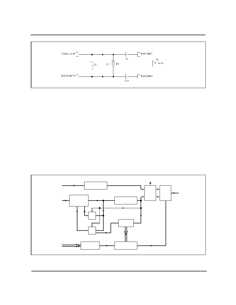
Figure 7 - External Transmit IF Filter
1.3 UHF LO and Frequency Doubler
Figure 7 also shows the UHF LO buffering and frequency doubler. The ZL20200 is designed to operate either with
separate external UHF VCOs for the 900 and 1900 MHz frequency bands, or alternatively a single 900 MHz VCO
can be used with the on-chip frequency doubler providing the LO for the 1900 MHz band. A UHF synthesizer is
included. The input to the UHF synthesizer will normally be the active UHF LO signal, however when using the
frequency doubler mode for 1900 MHz LO generation, the synthesizer input can be selected to be either the
frequency doubler output or the 900 MHz input LO signal. The UHF LO input buffer minimizes any load pulling
effects on the UHF VCO when internal modes are switched.
UHF LO output buffers are also provided. These can be used to drive an external mixer for the receive section. If
not required these buffers can be powered down.
1.4 UHF Frequency Synthesizer
A fractional N UHF synthesizer is included on the ZL20200 to provide LO signals for the transmit up-converter and
the external receive RF down-converters. The UHF synthesizer operates with an external VCO. A block diagram of
the synthesizer is shown in Figure 8.
.
Figure 8 - UHF Synthesizer
Reference Counter
14 bit
Quad Modulus
Prescaler
64/65/72/73
M Counter
13 bit
B
3 bit
A
4 bit
Fractional N
Counter
Fractional N
Scaling DAC
Fractional N
Compensation DAC
Phase
Detector
Charge
Pump
Lock Detect
TCXO
UHF LO
Frac N
Compensation
8 bits
UHF
CP
+1
+8
+1
5 bits
ZL20200
Data Sheet
17
Zarlink Semiconductor Inc.
The synthesizer uses a 4 modulus prescaler with an 'M' counter and 'A' and 'B' swallow counters together with a
fractional N counter in the UHF counter allowing maximum flexibility. The reference counter is a simple 14 bit
counter. All counter values are programmed via the serial bus and programming details are shown in the
programming section. Each of the counters operates as count down. At the start of a count the counters are loaded
with their respective values. The initial prescaler ratio is dependent on the values loaded into the A and B counters;
when both the A and B counters reach zero the prescaler ratio is 64 and then remains until the M counter reaches
zero. The complete process is then repeated.
This can be shown in a simple example where M = 9, A = 4 and B = 2 which gives a total divide ratio of 596. The
count sequence is shown in Figure 9.
Figure 9 - Count Sequence for UHF PLL with 4 Modulus Prescaler
At the start of the count sequence the '+1' and '+8' controls to the prescaler are both asserted and the prescaler
ratio is 73. After 2 cycles only the '+1' control is asserted and the divide ratio is 65. After a further 2 cycles the A
counter reaches zero as well and the prescaler ratio is 64 for the remainder of the count sequence. At the end of the
sequence all counters are reloaded and the sequence repeats.
The total divide ratio (N) for this type of counter is given by
N = 64*M + 8*B + A
M is always greater then A or B
A value of A = 0 does not support fractional N operation. Valid values of A are 1 to 8.
The values of M, B and A can be easily calculated from the total divide ratio as shown below.
M = INT ((N - 1)/64)
B = INT (((N - 1) - 64*M)/8)
A = N - 64*M - 8*B
The value of M must always be greater than A or B.
The maximum value of B is 7.
9
M Counter
A Counter
B Counter
Prescaler
+1 Prescaler
+8 Prescaler
8
7
6
5
4
3
2
1
9
8
4
3
2
1
0
0
0
0
0
4
3
2
1
0
0
0
0
0
0
0
2
1
73 73 65 65 64 64 64 64 64 73 73

ZL20200
Data Sheet
18
Zarlink Semiconductor Inc.
The UHF synthesizer also includes a fractional N capability which allows the use of higher comparison frequencies
but maintain narrow channel spacing. The use of higher comparison frequencies allows faster loop settling and
reduces comparison spur level. This is particularly important in TDMA mode where settling times of < 1.5 ms are
required and still obtain good spur performance.
Fractional N allows the use of non-integer divide ratios. For example if the total divide ratio is N + 1/5 the counter
will divide by N for 4 count cycles and N+1 on the fifth cycle giving the required total divide ratio over five cycles.
The ZL20200 can use 5,8,13 or 20 as the fractional denominator (also referred to as the fractional modulus)
allowing maximum flexibility in the choice of comparison frequencies.
An extra counter - fractional N counter - is required. The input to this counter is from the M counter output. The
fractional N modulus can be programmed to be 5,8,13, or 20. Each output pulse from the M counter will increment
the fractional N divided by the required fractional numerator. For example if the fraction is 2/5 then the fractional N
counter will increment by 2 for each output pulse from the M counter. When the fractional N counter overflows the A
counter is incremented by 1, thus generating an additional '+1' count sequence.
An example is shown in Figure 10 for a divide ratio of 596+2/5. The values for M, A, B are calculated using the
integer value (596) as in the previous example. The fractional denominator is programmed as 5 and the fractional
numerator as 2. At the end of the first count cycle (596) the fractional counter is incremented to 2. At the end of the
third count cycle the fractional N counter overflows, incrementing the A counter by 1 which gives a subsequent
count cycle of 597. After five count cycles the sequence repeats with a total count of 2982 over the five count cycle
giving a mean value of 596 + 2/5.
Figure 10 - UHF Synthesizer - Fractional N Operation
A result of this count sequence is that the output phase of the total counter changes through the count cycle, which
causes the output pulse from the phase detector, and therefore the charge pump, to vary. This would cause large
fractional spurs on the synthesizer output. These spurs can be compensated by applying a current pulse with the
opposite polarity to the charge pump output. This compensation pulse has a fixed width of two reference clock
(TCXO) periods; the amplitude is proportional to the value in the fractional N counter. The correction current is
scaled by a 8 bit compensation DAC, with an externally provided input from the serial bus. This allows performance
to be optimized in a given application.
The compensation value can be calculated from the following formula:
Comp Value = 255 - INT((Icp * Ftcxo)/(0.0245 * 6 * MOD *Fvco))
where
Icp
= charge pump current (uA)
596
596
597
596
2
4
1
3
597
596
2
0
0
Total Count Cycle
Count Value
Fractional N
Counter
Initial A
Counter
Value
4
4
5
4
4
5

ZL20200
Data Sheet
19
Zarlink Semiconductor Inc.
Ftcxo
= Reference frequency
MOD
= Fractional Modulus
Fvco
= UHF VCO Frequency
The synthesizer provides a lock detect output. When the output pulse from the phase detector is less than half a
reference clock period an in-lock signal is generated. These in-lock signals then clock a 4 bit counter into which a
threshold value has been programmed. When the required number of successive in-lock pulses have been
generated the lock detect output is set.
The ZL20200 has a single lock detect output pin for the UHF synthesizer and VHF synthesizers. The lock detect
signal is asserted when all active synthesizers are in lock. If a synthesizer has not been enabled in the power
control registers then that synthesizer will be inactive and will have no effect on the lock detect output.
1.5 VHF Frequency Synthesizers
The ZL20200 includes two VHF synthesizers to generate the second LO for the receiver and the transmit IF. They
operate with their respective on-chip VHF VCO's and off-chip loop filters. The tank circuits and tuning components
for the VCO's are also off chip.
The two synthesizers are identical and are shown in Figure 11.
Figure 11 - VHF Frequency Synthesizer
The synthesizer uses a 2 modulus 16/17 prescaler with an 'M' counter and an 'A' swallow counter. This allows
maximum flexibility when using this synthesizer. The reference counter is a simple 14 bit counter. All counter values
are programmed via the serial bus and programming details are shown in the programming section. Both counters
operate as count down. At the start of a count the counters are loaded with their respective values. The initial
prescaler ratio is 17 assuming A > 0; when the A counter reaches zero the prescaler ratio is 16 until the M counter
reaches zero. The complete process is then repeated.
The total divide ratio (N) for this type of counter is given by
N = 16*M + A
M is always greater then A
The values of M and A can be easily calculated from the total divide ratio N.
M = INT (N/16)
A = N - 16*M
Reference Counter
14 bit
Dual Modulus
Prescaler
16/17
M Counter
13 bit
A
4 bit
Phase
Detector
Charge
Pump
Lock Detect
TCXO
VHF LO
VHF
CP
+1

ZL20200
Data Sheet
20
Zarlink Semiconductor Inc.
The maximum value for A is 15 and M must always be greater than A. The VHF PLLs do not have fractional N
capability however it is recommended that they are operated at as high a comparison frequency as allowed by the
chosen frequency plan to minimize spurs levels.
Both VHF synthesizers have lock detection circuits. These operate in the same way as described for the UHF
synthesizer.
1.6 Internal Clock Generation
ZL20200 can use 14.4 MHz or 19.44 MHz reference frequency. The appropriate reference must be programmed
via the serial bus. The clock signals for the switched capacitor filters and FM demodulator are generated from the
reference TCXO signal. The internal divide ratios are switched to give the correct ratio.
Figure 12 - Typical VCO Tank Circuit
1.7 VHF VCO
ZL20200 has two VHF VCOs which operate with the VHF PLLs to provide the IF LO signals for both receive and
transmit IF signals. The oscillators are a differential design and require an external tank circuit. A basic circuit with
varactor is shown in Figure 12. It is recommended to include series resistors (e.g. 43 ohms) in each arm of the tank
circuit to prevent any spurious high frequency oscillation due to parasitic capacitances.
nm
33n
18p
18p
43R
43R
10k
10k
From PLL
Loop
Filter
VCO+
VCO-
ZL20200
Data Sheet
21
Zarlink Semiconductor Inc.
1.8 Power Supply Connections
The circuit blocks within ZL20200 have separate supply connections to minimize interaction between circuit blocks.
Details are shown in the earlier `Pin Names' section. These supplies are also grouped to allow different groups of
supply pins to be connected to separate supplies for example, receive or transmit. These groups are shown below:
The LO OUT and TX 900/1900 pins require bias and are normally connected to VCC through an inductor.
All supply pins within a group must be powered together. Each group of pins can be powered up independent of the
other groups.
VCC � Control Supply
Pin No.
Pin Name
56
VCC CONTROL
VCC � TxRx Common (Synth)
Pin No.
Pin Name
5
VCC UHF PLL
7
VCC UHF LO OUT
13
VCC UHF LO
38
VCC VHF CP
8
900 LO OUT
9
1900 LO OUT
VCC � Rx
Pin No.
Pin Name
49
VCC RX PLL
50
VCC RX
VCC � Tx
Pin No.
Pin Name
15
VCC TX RF
24
VCC TX
31
VCC TX PLL
16
TX 900
19 TX
1900
Table 4 - Power Supply Connections

ZL20200
Data Sheet
22
Zarlink Semiconductor Inc.
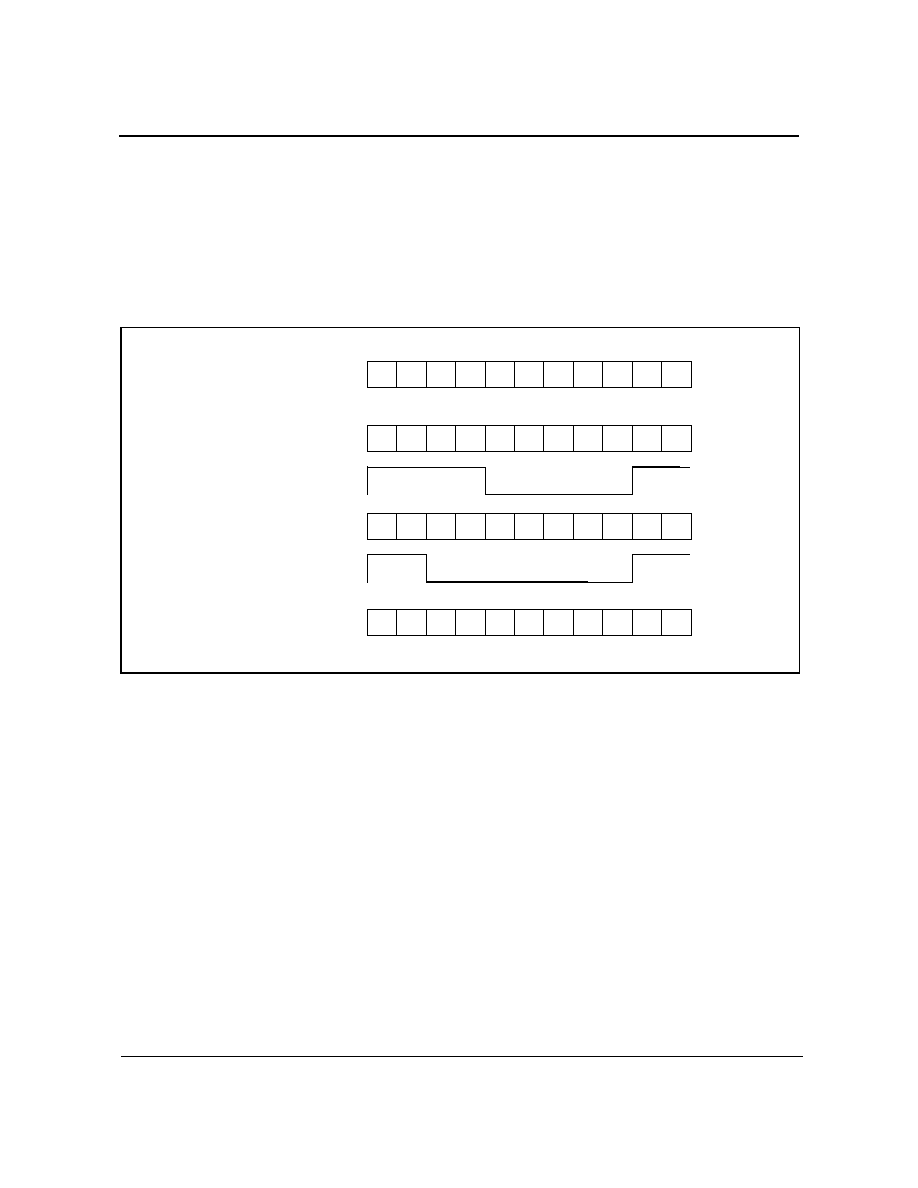
2.0 Programming and Control
Programming via the serial bus is via 24 bit words with a 4 bit address as shown below
Bit23 (MSB) is loaded first. Bits 3:0 are used as address bits for the control registers. Details of serial bus timing are
shown in Figure 13.
Figure 13 - Serial Bus Timing
Enable1 and Enable2 need only be asserted after loading registers 0 to 3, the power control registers. These
registers should be loaded with Enable1 and Enable2 low. All other registers can be loaded with Enable1 and
Enable2 high or low.
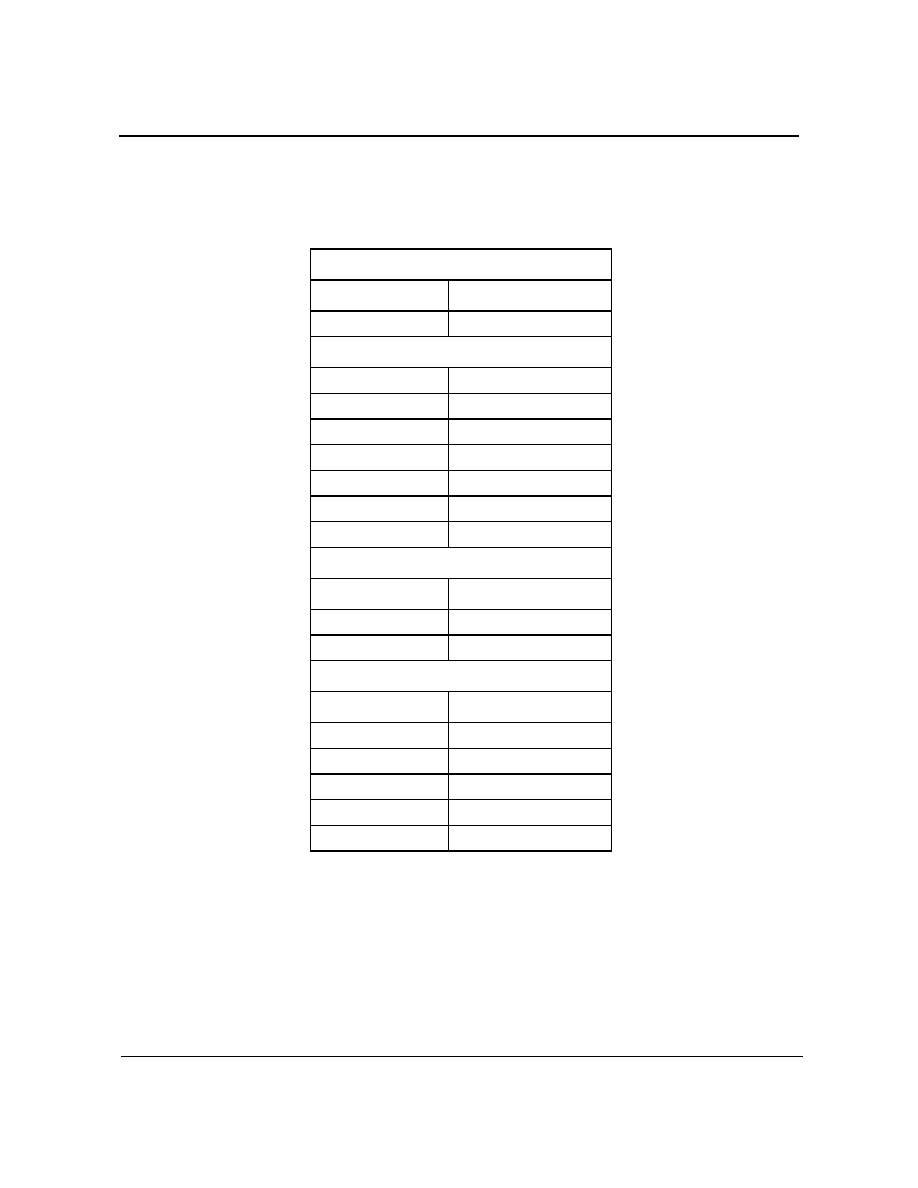
2.1 Power Control Registers - Address 0 to 3
These registers are used in conjunction with the TX RXB and ENABLE1 and ENABLE2 control pins to power up the
required sections of the device for any required mode. This enables power consumption to be optimized under all
conditions. Figures 4 - 7, which show the receive and transmit paths in detail, show which sections are powered up
by each control bit.
23
22
21
20
19
18
17
17
15
14
13
12
11
10
9
8
7
6
5
4
3
2
1
0
Data
Address
SCLK
SDAT
SLATCH
Bit 23
Bit 22
Bit 21
Bit 0
t1
t2
t3
t4
t5
t6
ENABLE1/2
t7

ZL20200
Data Sheet
23
Zarlink Semiconductor Inc.
The assignment is common for each of the registers 0 to 3 and is shown below.
Note 1: If a bit is set to logic 1 then that circuit section is powered on.
Note 2: UHF LO input (bit 9) must be enabled for Transmit UHF LO (bit 10), UHF synthesizer (bit 19) and UHF LO Buffer (bit 21) to be
active.
Bit
Circuit Section
23
Not used
22
Receive Baseband section
21
UHF LO Buffer
20
Receive VHF VCO
19
UHF synthesizer
18
Receive RSSI circuit
17
Not used
16
Receive Quadrature down-converter
15
Receive VHF PLL
14
Receive IF input
13
Receive AGC amplifier
12
Transmit reconstruction filters
11
Transmit RF
10
Transmit UHF LO
9
UHF LO input buffer
8
Transmit IF
7
Transmit quadrature modulator
6
Transmit VHF PLL
5
Transmit VHF VCO
4
Transmit up-converter IF input
Table 5 - Power Control Registers

ZL20200
Data Sheet
24
Zarlink Semiconductor Inc.
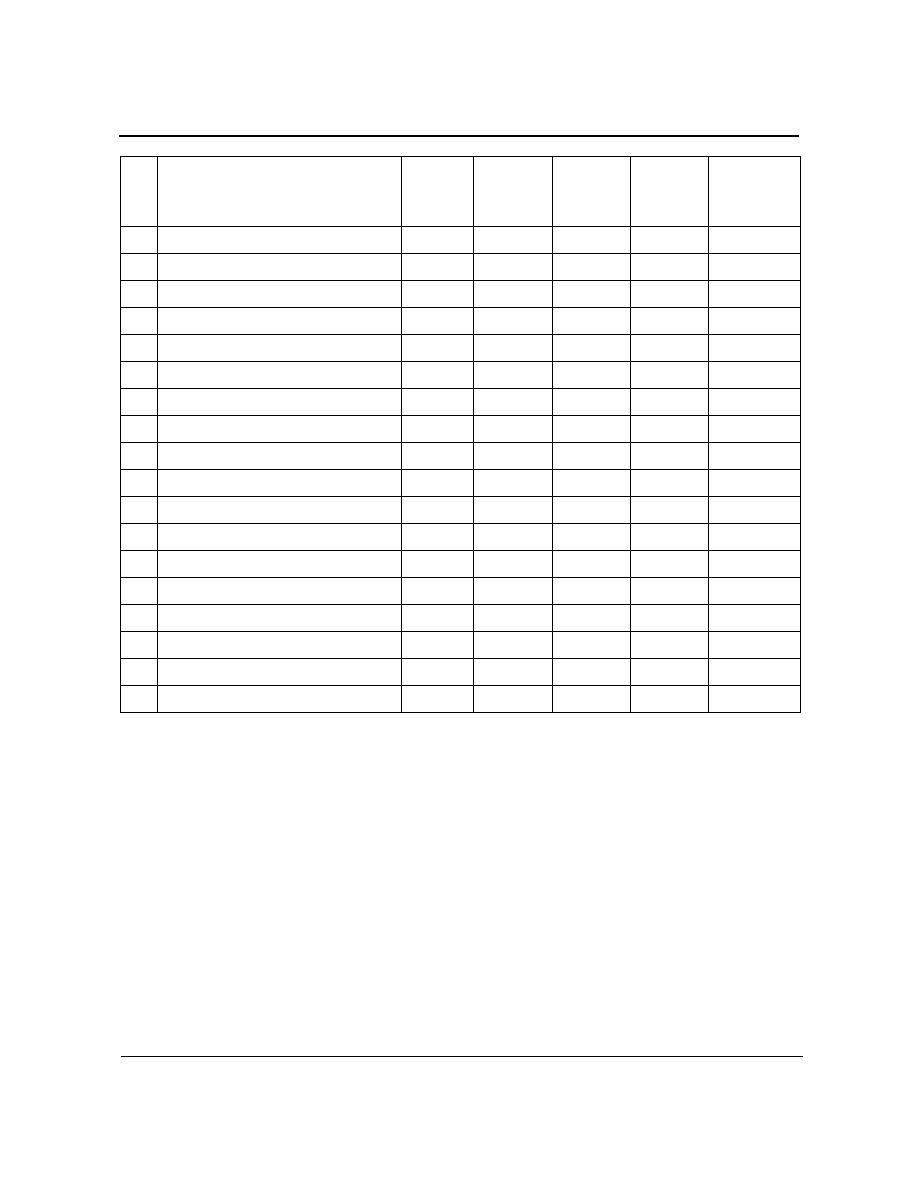
The 4 registers address 0 to 3 are assigned as follows:
A feature of this programming approach is that once a phone operating mode has been selected and set up via the
serial bus, all power control can then be via the TX RXB, ENABLE1 and ENABLE2 control pins. Alternatively full
power control is possible via the 3 wire serial bus without the use of any external control pins.
If ENABLE1 and ENABLE2 are both low then the device is in Sleep mode. No circuits will be enabled unless either
ENABLE1 or ENABLE2 are high regardless of the contents of the receive and transmit registers.
An example of how these control bits can be used, is that the oscillators and PLL circuits can be powered up and
allowed to settle prior to powering up the complete transmit or receive path. In the case of the receive path the UHF
synthesizer, UHF LO input buffer, UHF LO Buffer and Receive VHF VCO, Receive VHF PLL bits would be set in the
ENABLE1 Configuration register. The ENABLE2 Configuration register would contain these bits plus the remainder
of the receive path bits, Receive IF input, Receive AGC amplifier, Receive quadrature down-converter and receive
baseband section.
This is demonstrated in the following examples.
2.1.1 Power Control Modes - TDMA (IS136)
In a TDMA system the transceiver will either operate in receive only, or transmit only mode. It is assumed that an
interim power on state will be used during which the oscillators and PLLs will be set up, and allowed to settle prior
to activating the full signal path. The suggested programming for the power control registers (0 - 3) is shown in the
table below.
Register
Address
Register
Name
Description
0
Receive
All circuit blocks required in receive mode should be set to 1. This register will be
selected when TX RXB is low. No circuits will be actually powered up if ENABLE1
and ENABLE 2 are both low.
1
Transmit
Transmit register All circuit blocks required in transmit mode should be set to 1. In
duplex modes e.g. AMPS then both receive and transmit circuits must be selected.
This register will be selected when TX RXB is high. No circuits will be actually
powered up if ENABLE1 and ENABLE 2 are both low
2
ENABLE1
Configuration
This register determines which circuit sections are powered up when ENABLE1 is
high. The contents of this register are logical ANDed with the contents of the
Receive or Transmit register as selected by TX RXB input.
3
ENABLE2
Configuration
This register determines which circuit sections are powered up when ENABLE2 is
high. The contents of this register are logical ANDed with the contents of the
Receive or Transmit register as selected by TX RXB input.
Table 6 - Power Control Register Functions
Bit
Circuit
Section
Receive
Addr 0
Transmit
Addr 1
Enable 1
Config.
Addr 2
Enable 2
Config.
Addr 3
Comments
23
Not used
0
0
0
0
22
Receive Baseband section
1
0
0
1
Table 7 - Programming for the Power Control Registers (0 - 3)
ZL20200
Data Sheet
25
Zarlink Semiconductor Inc.
Note 1:
Not required if driving external receive mixer direct from UHF VCO.
Note 2:
Can be used for IS136 if required.
The receive register contains all bits required when in receive mode: the transmit register contains all bits required
in transmit mode. The Enable1 configuration register contains all bits required to power up oscillators and
synthesizers in both receive and transmit mode. The Enable2 configuration register contains all bits required to
power up the complete receive and transmit modes (this register can be set to all '1's if preferred).
The following words should therefore be programmed on the serial bus (Hex format):
Receive register (0)
59E200
Transmit register (1)
081FF1
Enable1 Config. register (2)
188262
Enable2 Config. register (3)
59FFF3
21
UHF LO Buffer
0
0
0
0
Note 1
20
Receive VHF VCO
1
0
1
1
19
UHF synthesizer
1
1
1
1
18
Receive RSSI circuit
0
0
0
0
Note 2
17
Not used
0
0
0
0
16
Receive Quadrature down-converter
1
0
0
1
15
Receive VHF PLL
1
0
1
1
14
Receive IF input
1
0
0
1
13
Receive AGC amplifier
1
0
0
1
12
Transmit reconstruction filters
0
1
0
1
11
Transmit RF
0
1
0
1
10
Transmit UHF LO
0
1
0
1
9
UHF LO input buffer
1
1
1
1
8
Transmit IF
0
1
0
1
7
Transmit quadrature modulator
0
1
0
1
6
Transmit VHF PLL
0
1
1
1
5
Transmit VHF VCO
0
1
1
1
4
Transmit up-converter IF input
0
1
0
1
Bit
Circuit
Section
Receive
Addr 0
Transmit
Addr 1
Enable 1
Config.
Addr 2
Enable 2
Config.
Addr 3
Comments
Table 7 - Programming for the Power Control Registers (0 - 3) (continued)

ZL20200
Data Sheet
26
Zarlink Semiconductor Inc.
2.1.2 Power Control Modes - AMPS
When operating in AMPS mode the ZL20200 will operate in either Receive only or Duplex. The enable registers
should therefore be programmed as shown below.
Note 1: Not required if driving external receive mixer direct from UHF VCO.
The receive register contains all bits required when in receive mode: the transmit register contains all bits required
in duplex mode. The Enable1 configuration register contains all bits required to power up oscillators and
synthesizers in both receive and duplex mode. The Enable2 configuration register contains all bits required to
power up the complete receive and duplex modes (this register can be set to all '1's if preferred).
The following words should therefore be programmed on the serial bus (Hex format):
Receive register (0)
5DE200
Transmit register (1)
5DFFF1
Bit
Circuit Section
Receive
Addr 0
Transmit
Addr 1
Enable 1
Config.
Addr 2
Enable 2
Config.
Addr 3
Comments
23
Not used
0
0
0
0
22
Receive Baseband section
1
1
0
1
21
UHF LO Buffer
0
0
0
0
Note 1
20
Receive VHF VCO
1
1
1
1
19
UHF synthesizer
1
1
1
1
18
Receive RSSI circuit
1
1
0
1
17
Not used
0
0
0
0
16
Receive Quadrature down-
converter
1
1
0
1
15
Receive VHF PLL
1
1
1
1
14
Receive IF input
1
1
0
1
13
Receive AGC amplifier
1
1
0
1
12
Transmit reconstruction filters
0
1
0
1
11
Transmit RF
0
1
0
1
10
Transmit UHF LO
0
1
0
1
9
UHF LO input buffer
1
1
1
1
8
Transmit IF
0
1
0
1
7
Transmit quadrature modulator
0
1
0
1
6
Transmit VHF PLL
0
1
1
1
5
Transmit VHF VCO
0
1
1
1
4
Transmit up-converter IF input
0
1
0
1
Table 8 - Enable Registers
ZL20200
Data Sheet
27
Zarlink Semiconductor Inc.
Enable1 Config. register (2)
188262
Enable2 Config. register (3)
5DFFF3
2.2 Operating Register Address 4
This registers selects internal setups for example IS136. The bits are assigned for control of receive and transmit
bits as shown below:
The function of the receive bits is shown below:
Bit 23 RX<7> is only applicable when VCO divide by 2 mode is selected in register 5
23
22
21
20
19
18
17
16
15
14
13
12
11
10
9
8
7
6
5
4
3
2
1
0
RX<7:0>
TX <11:0>
0
1
0
0
Receive Set Up
Transmit Set Up
Address
Register
Bit No.
Control
Bit
Action if '0'
Action if '1'
23
RX<7>
Receive DLL disabled
Receive DLL enabled
22
RX<6>
Bandpass Filter BW = +/- 20 kHz
Bandpass Filter BW = +/- 16 kHz
21
RX<5>
Not Used. Set to `0'.
20
RX<4>
LO output = 900 MHz
LO Output = 1900 MHz
19
RX<3>
Receive output dc bias (I/Q) = 1.25 V
Receive output dc bias (I/Q) = Vcc/2
18
RX<2>
IS136 Mode IF1 Input enabled
Not Used
17
RX<1>
AMPS
IS136
16
RX<0>
IF Input 0 selected
IF Input 1 selected
Table 9 - Function of the Receive Bits
ZL20200
Data Sheet
28
Zarlink Semiconductor Inc.
The function of the transmit bits is shown below:
Control bits TX<11:4> allow optimization of the transmit output stage. This allows variation of the decrease in
supply current with decreasing agc voltage and also allows optimization depending on output power and linearity
requirements. Figure 14 shows the variation of output stage supply current with agc voltage and the programmable
characteristics. The maximum current, agc threshold and slope can be programmed. The minimum current is not
programmable.
TX<11:10> (bits 15,14) allow the gain of the transmit output stage to be varied in 3 dB steps as shown in the table
below:
Register Bit
No.
Control
Bit
Action if '0'
Action if '1'
15
TX<11>
Transmit output stage gain control
14
TX<10>
13
TX<9>
Control of RF Transmit output stage current with VGA control voltage.
Nominal value for TX<11:4> is 101010
12
TX<8>
11
TX<7>
10
TX<6>
9
TX<5>
8
TX<4>
7
TX<3>
900 MHz output
1900 MHz output
6
TX<2>
Internal
External transmit IF Filter
5
TX<1>
IS136 baseband filters
Not Used
4
TX<0>
Transmit baseband filters selected
Transmit baseband filters by-passed
Table 10 - Function of the Transmit Bits
TX<11>
TX<10>
Gain (dB)
0
0
-6
0
1
-3
1
0
Nominal
1
1
+3
Table 11 - Gain of the Transmit Output Stage

ZL20200
Data Sheet
29
Zarlink Semiconductor Inc.
Figure 14 - Transmit Output Stage Current versus Gain Control
TX<9:8> (bits 13:12) control the agc voltage (Vth) at which the output stage current starts reducing. Typical values
are shown in the table below:
TX<7:6> (bits 11,10) control the rate of current reduction as shown in Figure 14. Typical vales are shown in the
below:
TX<5:4> (bits 9:8) adjust the maximum current (Imax) of the transmit output stage. The gain of the output stage is
not changed. Typical values are shown in the table below:
TX<9>
TX<8>
Vth (V)
0
0
1.09
0
1
1.25
1
0
1.48
1
1
1.81
Table 12 - VGA Threshold Voltage
TX<7>
TX<6>
Slope (mA/V)
0
0
65
0
1
75
1
0
90
1
1
105
Table 13 - VGA Current Reduction
TX<5>
TX<4>
Current
0
0
25%
0
1
50%
1
0
Nominal
1
1
150%
Table 14 - Output Stage Current
Vagc
Icc
Imax
Imin
Vth
Slope

ZL20200
Data Sheet
30
Zarlink Semiconductor Inc.
Using these controls allows the performance of the output stage to be optimized under various conditions; for
example, current cant can be reduced if non-linear operation is required.
The nominal value recommended for TX<11:4> is 10101010.
An example of setting up the control register (address 4) for various systems is shown below:
Note 1: The setting for RX<3> is dependent on the optimum common mode input voltage of the analog to digital converter in the
baseband.
Note 2: Selects external transmit IF filter if used.
The following hex words are therefore recommended for the control register (address 4):
IS136 (900)
03AA04
IS136 (1900)
13AAC4
AMPS
41AA04
Bit
Name
IS136 - (900)
IS136 - (1900)
AMPS
Comments
23
RX<7>
0
0
0
22
RX<6>
0
0
1
21
RX<5>
0
0
0
20
RX<4>
0
1
0
19
RX<3>
0
0
0
Note 1
18
RX<2>
0
0
0
17
RX<1>
1
1
0
16
RX<0>
1
1
1
15
TX<11>
1
1
1
14
TX<10>
0
0
0
13
TX<9>
1
1
1
12
TX<8>
0
0
0
11
TX<7>
1
1
1
10
TX<6>
0
0
0
9
TX<5>
1
1
1
8
TX<4>
0
0
0
7
TX<3>
0
1
0
6
TX<2>
0
1
0
Note 2
5
TX<1>
0
0
0
4
TX<0>
0
0
0
Table 15 - Control Register Settings

ZL20200
Data Sheet
31
Zarlink Semiconductor Inc.
2.3 Synthesizer Register - Address 5
This register sets up LO options for receive and transmit and also UHF synthesizer set up.
Bits 23,17,14 are also used for UHF PLL and LO set up.
Bits 16,15 are not used and should be set to zero.
2.3.1 UHF PLL and LO
Note 1: Bit 14 is only effective if 1900 MHz mode has been selected (register 4 Bit 7).
Note 2: Bit 23 is only effective if 1900 MHz mode has been selected (register 4 Bit 7) and the UHF frequency doubler selected
(Register 5 Bit 14). This control allows the use of the doubled frequency to be used as the input to the UHF PLL.
Note 3: Fractional N Denominator.
Note 4: Bits 8,7 select the fractional N denominator for the UHF PLL as shown below:
23
22
21
20
19
18
17
16
15
14
13
12
11
10
9
8
7
6
5
4
3
2
1
0
0
0
1
0
1
UI
RX LO2 Set Up
UC
DL
UD
TX LO Set Up
UHF PLL Set Up
Address
Register Bit No.
Action if '0'
Action if '1'
23
UHF PLL input = 900 MHz
UHF PLL input = 1900 MHz
17
Fractional N Compensation selected
14
UHF Doubler Selected
8
Fractional N Denominator - see table below
7
6
Not Used - Set to 0
5
UHF PLL Charge Pump Current - see table below
4
Table 16 - UHF PLL and LO Control
<8>
<7>
Frac N Denom.
0
0
5
0
1
8
1
0
13
1
1
20
Table 17 - Fractional N Denominator

ZL20200
Data Sheet
32
Zarlink Semiconductor Inc.
2.3.2 UHF PLL Charge Pump Current
Bits 5,4 select the charge pump current for the UHF PLL as shown below:
2.3.3 Receive LO Set Up
Bits 19,18 select the charge pump current for the receive VHF PLL as shown below:
<5>
<4>
Current (mA)
0
0
1.00
0
1
0.50
1
0
0.25
1
1
0.125
Table 18 - UHF PLL Charge Pump Current
Register Bit No.
Action if '0'
Action if '1'
22
High side Rx second LO injection
Low side Rx second LO injection
21
Rx second LO = VCO/2
Rx second LO = VCO/4
20
Rx LO phase detector polarity normal
Rx LO phase detector polarity inverted
19
Receive VHF PLL Charge Pump Current - see table below
18
Table 19 - Receive LO Set Up
<19>
<18>
Current (mA)
0
0
1.00
0
1
0.50
1
0
0.25
1
1
0.125
Table 20 - Receive VHF PLL Charge Pump Current
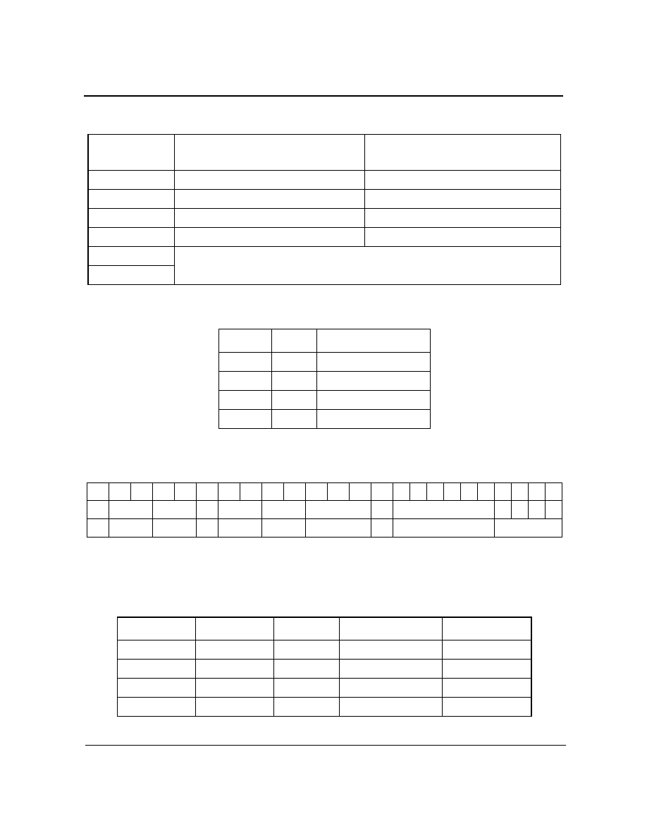
ZL20200
Data Sheet
33
Zarlink Semiconductor Inc.
2.3.4 Transmit LO Set Up
Bits 10,9 select the charge pump current for the receive VHF PLL as shown below:
2.4 Control Register - Address 6
2.4.1 IS136 Baseband Gain
Bits 22:21 can be used to vary the gain of the baseband output stages in IS136 mode only. The gain of the 60 kHz
IF stage preceding the baseband mixer is also varied so that the overall gain of the device can be maintained if
required. The nominal gain is 20 dB and the recommended setting is BBG<1:0> = 11 to minimize output dc offsets.
Register
Bit No.
Action if '0'
Action if '1'
15
Transmit DLL disabled
Transmit DLL enabled
13
Low side Tx up-converter LO injection
High side Tx up-converter LO injection
12
Tx second LO = VCO/2
Tx second LO = VCO/4
11
Tx LO phase detector polarity normal
Tx LO phase detector polarity inverted
10
Transmit VHF PLL Charge Pump Current - see table below
9
Table 21 - Transmit LO Set Up
<10>
<9>
Current (mA)
0
0
1.00
0
1
0.50
1
0
0.25
1
1
0.125
Table 22 - Transmit VHF PLL Charge Pump Current
23
22
21
20
19
18
17
16
15
14
13
12
11
10
9
8
7
6
5
4
3
2
1
0
0
0
0
1
1
0
BBG
TCXO
PDF
LPC
Tx Gain
R
Mode Control
Address
BBG<1> Bit 22
BBG<0> Bit 21
IF Gain (dB)
Baseband Gain (dB)
Overall Gain (dB)
0
0
14
6
20
0
1
17
6
23
1
0
17
0
17
1
1
20
0
20
Table 23 - Baseband Gain
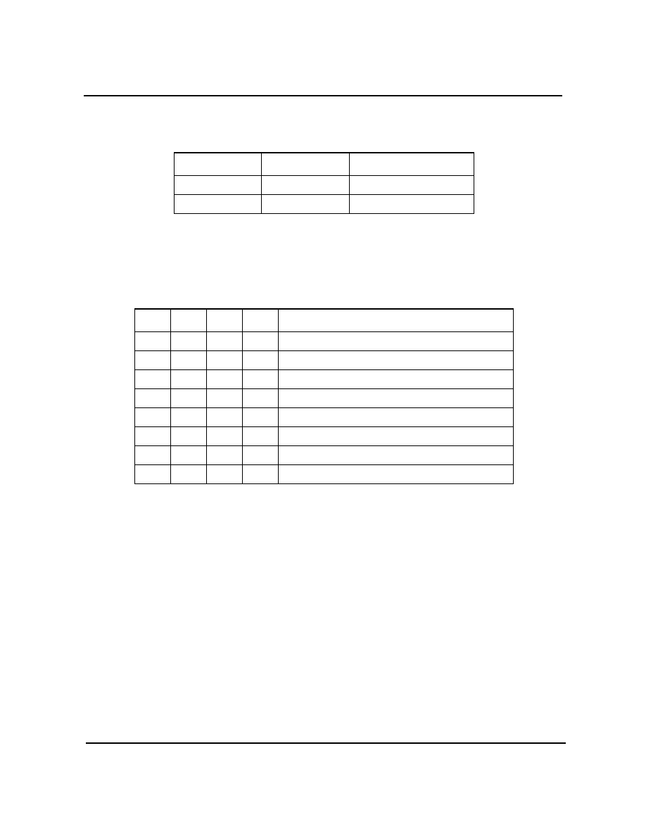
ZL20200
Data Sheet
34
Zarlink Semiconductor Inc.
2.4.2 TCXO Reference Selection
Bits 20:19 are used to set the device to the required TCXO reference frequency.
2.4.3 Discriminator Output Filtering
Bits 17:14 set up on chip filtering of the FM output signal and are therefore only used in AMPS mode. Two
cascaded filters can be selected and the bandwidth can be set to 25 or 37.5 kHz cut-off. Bits 17,16 (PDF) select the
filters and bits 15,14 set the cutoff frequency.
In IS136 mode Bits <17:14> should be set to 0000. It is recommended that if the additional discriminator filtering is
required in AMPS mode then both filters should be used with 25 kHz bandwidth, i.e. Bits<17:14> should be set
1111.
TCXO<1> Bit 20
TCXO<0> Bit 19
TCXO Frequency (MHz)
0
1
14.4
1
0
19.44
Table 24 - TCXO Reference Selection
<17>
<16>
<15>
<14>
Filter Selection
0
0
X
X
No filters
0
1
X
X
Filter 1 selected
1
0
X
X
Filter 2 selected
1
1
X
X
Filters 1 and 2 selected
X
X
0
0
Both filters 37.5 kHz
X
X
0
1
Filter 1 25 kHz, Filter 2 37.5 kHz
X
X
1
0
Filter 1 37.5 kHz, Filter 2 25 kHz
X
X
1
1
Both filters 25 kHz
Table 25 - FM Discriminator Output Filter Control
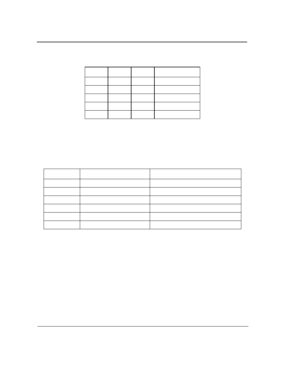
ZL20200
Data Sheet
35
Zarlink Semiconductor Inc.
2.4.4 Transmit Baseband Gain
Bits 13:11 set the transmit baseband gain as shown below:
2.4.5 Mode Control
Bit 10 resets the contents of all registers to '0'. After the reset is complete bit 10 is also reset to '0'.
Bits 9:4 allow TXRXB, ENABLE1 and ENABLE2 to be programmed by either the external pins or via the serial bus.
This allows mode control to be either via the external pins or the serial bus. The default state is using the external
pins as this allows more accurate timing of power control.
Bits 9:7 can only be used if the appropriate bits 6:4 have been set to disable the external pins. If serial mode has
been selected then the operation of bits 9:7 is the same as the external TX RXB, ENABLE1 and ENABLE2 pins
respectively.
2.5 Register Address 7 - Not Used
2.6 Test Mode Register - Address 8
This register is used for test purposes only and should not be used.
<13>
<12>
<11>
Gain (dB)
0
0
0
0
0
0
1
3
0
1
0
6
0
1
1
9
1
0
0
12
Table 26 - Transmit Baseband Gain
Register Bit No.
Action if '0'
Action if '1'
9
Receive Register (0) selected
Transmit Register (1) selected
8
Enable2 Configuration Register (3) selected
7
Enable1 Configuration Register (2) selected
6
TXRXB Pin (34) selected
Serial Bus selected - Bit 9
5
Enable2 Pin (20) selected
Serial Bus selected - Bit 8
4
Enable1 Pin (11) selected
Serial Bus selected - Bit 7
Table 27 - Mode Control
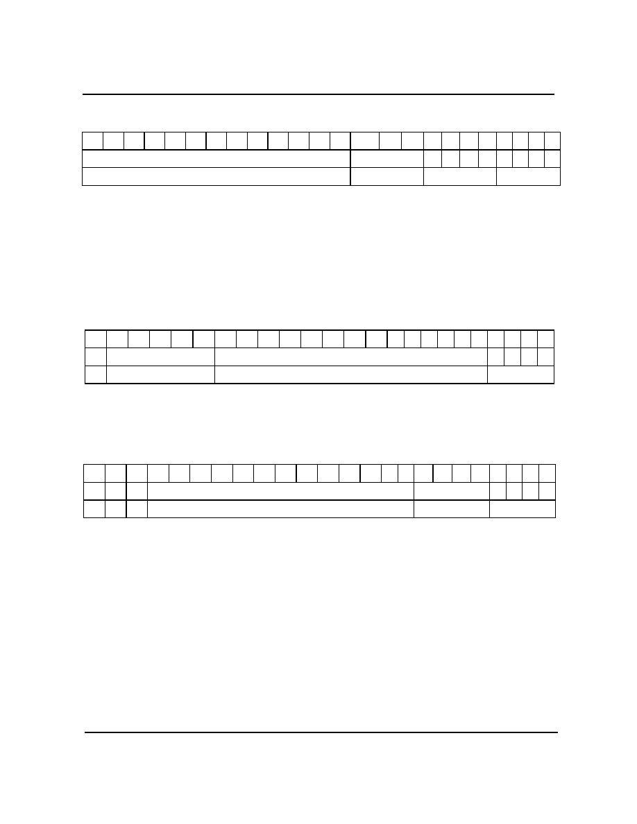
ZL20200
Data Sheet
36
Zarlink Semiconductor Inc.
2.7 UHF PLL Divider Programming Register - Address 9
Bits 23:11 set M counter value (Bit 23 = MSB)
Bits 10:8 set B counter value - max value = 7 (Bit 10 = MSB)
Bits 8:4 set A counter value - max value = 8 (Bit 7 = MSB)
The A counter is a 4 bit counter to enable correct fractional N operation. Valid values of A are in the range 1 to 8.
Using the 64/65/72/73 four modulus prescaler the divide ratio (N) is given by:
N = 64 * M + 8 * B + A
Values of M, B, A can be easily calculated using the formulae in the synthesizer section.
2.8 UHF PLL Reference Divider and Fractional N Programming Register - Address 10
Bit 23 is unused and should be set to '0'
Bits 22:18 set the fractional N numerator (Bit 22 = MSB)
Bits 17:4 set the Reference counter value (Bit 17 = MSB)
2.9 Receive VHF PLL Divider Programming Register - Address 11
Bits 20:8 set M counter value (Bit 20 = MSB)
Bits 7:4 set A counter value - max value = 15 (Bit 7 = MSB)
Using the 16/17 two modulus prescaler the divide value (N) is given by:
N = 16 * M + A
Values of M, A can be easily calculated using the formulae in the synthesizer section.
23
22
21
20
19
18
17
16
15
14
13
12
11
10
9
8
7
6
5
4
3
2
1
0
1
0
0
1
M Counter Value
B Counter Value
A Counter Value
Address
23
22
21
20
19
18
17
16
15
14
13
12
11
10
9
8
7
6
5
4
3
2
1
0
0
1
0
1
0
X
Frac N Numerator
UHF PLL Reference Counter Value
Address
23
22
21
20
19
18
17
16
15
14
13
12
11
10
9
8
7
6
5
4
3
2
1
0
0
0
0
1
0
1
1
X
X
X
M Counter Value
A Counter Value
Address

ZL20200
Data Sheet
37
Zarlink Semiconductor Inc.
2.10 Receive VHF PLL Reference Divider Programming Register - Address 12
Bits 23:19 are unused and should be set to '0'
Bit 18 selects common reference divider for VHF receive and transmit PLLs ('0' to select). If a common reference
divider is selected then the transmit VHF reference divider is used which must be programmed in register 13.
Bits 17:4 set the Reference divider value (Bit 17 = MSB)
2.11 Transmit VHF PLL Divider Programming Register - Address 13
Bits 23:21 are unused and should be set to '0'
Bits 20:8 set M counter value (Bit 20 = MSB)
Bits 7:4 set A counter value - max value = 15 (Bit 7 = MSB)
Programming is identical to that for the receive VHF PLL register 11.
2.12 Transmit VHF PLL Reference Divider Programming Register Address 14
Bits 23:18 are unused and should be set to '0'
Bits 17:4 set the Reference counter value (Bit 17 = MSB)
2.13 PLL Lock Detect & Fractional N Compensation Programming Register Address 15
2.13.1 Fractional N Compensation
Bits 23:16 set the value for fractional N compensation in the UHF PLL with bit 23 as MSB. The value for the
compensation is dependent on a number of parameters which are described in the synthesizer section.
23
22
21
20
19
18
17
16
15
14
13
12
11
10
9
8
7
6
5
4
3
2
1
0
0
0
0
0
0
1
1
0
0
X
X
X
X
X
RS
Receive VHF PLL Reference Counter Value
Address
23
22
21
20
19
18
17
16
15
14
13
12
11
10
9
8
7
6
5
4
3
2
1
0
0
0
0
1
1
0
1
X
X
X
M Counter Value
A Counter Value
Address
23
22
21
20
19
18
17
16
15
14
13
12
11
10
9
8
7
6
5
4
3
2
1
0
0
0
0
0
0
0
1
1
1
0
X
X
X
X
X
X
Transmit VHF PLL Reference Counter Value
Address
23
22
21
20
19
18
17
16
15
14
13
12
11
10
9
8
7
6
5
4
3
2
1
0
1
1
1
1
Fractional N Compensation
UHF PLL
Lock Count
Transmit VHF PLL
Lock Count
Receive VHF PLL
Lock Count
Address
ZL20200
Data Sheet
38
Zarlink Semiconductor Inc.
2.13.2 PLL Lock detect counters
These 4 bit counters count the consecutive comparison cycles where the lock detect circuit gives an in-lock result.
When the counter reaches its programmed count then that PLL is deemed to have achieved full lock. This prevents
spurious false in-lock signals while the PLL is achieving lock up. There are separate counters for the UHF, Rx VHF
and Tx VHF PLLs which are programmed as shown above. Bits 15,11,7 are the MSB's for the UHF, Rx VHF and Tx
VHF PLL lock detector counters respectively. A non zero value must be programmed for the lock detect to operate
correctly.
3.0 Absolute Maximum Ratings
This device is sensitive to ESD. Most pins have an ESD rating greater than 2000 V (Human Body Model HBM),
however some pins have limited protection (800 to 2000 V) in order to meet the RF performance requirements.
Anti-static precautions should be used when handling this device.
4.0 Operating Conditions
Device operation is guaranteed under the following conditions:
Supply Voltage
-0.3 to 3.6 V
Voltage applied to any pin
-0.3 to Vcc + 0.3 V
Operating Temperature
-40�C to 85�C
Storage Temperature
-55�C to 125�C
Max Junction Temperature
125�C
Operating Conditions
Condition
Min.
Value Type
Max.
Units
Comments
General
Supply Voltage
2.7
3.3
V
Operating Temperature
-40
+85
�C
Logic Input Voltage High � VIH
0.8Vcc
Volts
Logic Input Voltage Low � VIL
0.2Vcc
Volts
TCXO Reference Frequency
Frequency
14.4
MHz
Frequency
19.44
MHz
Receiver
Receiver IF Frequency
70
215
MHz

ZL20200
Data Sheet
39
Zarlink Semiconductor Inc.
Transmitter
Transmit IF Frequency
50
215
MHz
I & Q common mode voltage
1.2
V
I & Q input voltage level
1.5
V p-p
0dB input buffer gain
Cellular band LO input level
-15
-10
-5
dBm
PCS band LO input level
-15
-10
-5
dBm
Cellular band LO frequency
900
1100
PCS1900 band frequency
1900
2200
MHz
Serial Control Timing
See Figure 13
SDATA Set Up t1
20
ns
SDATA Hold t2
20
ns
SCLK Pulse Width t3
50
ns
SLATCH Set up t4
20
ns
SLATCH Pulse Width t5
50
ns
SCLK Period t6
100
ns
Power Control Set up t7
20
ns
Operating Conditions (continued)
Condition
Min.
Value Type
Max.
Units
Comments

ZL20200
Data Sheet
40
Zarlink Semiconductor Inc.
5.0 Electrical Characteristics
The electrical characteristics are guaranteed under the following conditions unless stated otherwise. Vcc =3.0 V, T
= 25�C, TCXO Ref Frequency = 19.44 MHz.
Characteristics
Min.
Value
Typ
Max.
Units
Comments
Supply Current
Sleep
10
40
�A
Logic inputs = 0 V or Vcc
Receive Operation
AMPS
32
38
mA
Note 1, AGC = 1.6 V
IS136
33
39
mA
Note 1, AGC = 1.6 V
Transmit Operation
900 MHz Output
141
170
mA
VGA = 2.4 V, Note 2
106
125
mA
VGA = 1 V, Note 2
1900 MHz Output
120
145
mA
VGA = 2.4 V, Note 2
102
120
mA
VGA = 1 V, Note 2
Standby Operation
UHF PLL
12.5
15.0
mA
Note 3
Receive VHF PLL
5.2
6.3
mA
Transmit VHF PLL
4.9
6.0
mA
Additional Circuits
Frequency Doubler
4
5
mA
Note 4
UHF LO Output Buffer
4.5
5.5
mA
900 or 1900 Band Note 5
Logic Inputs
Input Current
10
nA
Vin = 0 to Vcc
Input Capacitance
10
pF
Lock Detect Output
Output Voltage Low
0.2Vcc
Volts
I out = 1 mA
Output Voltage High
0.8Vcc
Volts
I out = -1 mA
TCXO Input
ZL20200
Data Sheet
41
Zarlink Semiconductor Inc.
Input Resistance
10
k
Input Capacitance
10
pF
Input Sensitivity
0.5
2
V p-p
ac coupled
Receiver - IS136
All parameters are measured at an IF
frequency of 135.06 MHz, Rx VCO = 270
MHz unless stated otherwise
Input impedance
500
1500
W
Max Voltage Gain
80
91
dB
AGC = 2.4 V
Min Voltage Gain
-13
5
dB
AGC = 0.3 V
Gain slope
50
56
62
dB/V
AGC = 0.3 to 2 V
NF Gainmax
8
dB
Rs =800
Input V1dB Gainmin
101
104
dB
�V
Minimum gain
IIP3 Gainmax
74
dB
�V
Max Gain
I/Q Amplitude Matching
+/- 0.5
dB
I/Q Quadrature Accuracy
+/- 2
�
Output 1 dB Compression
3
V p-p
Output dc Offset
+/-20
mV
Receiver AMPS
(Fixed Gain)
All parameters are measured at an IF
frequency of 135.06 MHz, Rx VCO = 270
MHz unless stated otherwise.
Vagc = 1.6 V (Gain 20 dB below
maximum)
Input impedance
500
1500
W
Input Sensitivity
14
dB
�V
Note 6
Noise Figure
12
dB
Input IP3
93
dB
�V
Audio Output
900
1000
1100
mV
Note 7
RSSI Dynamic Range
50
dB
Accuracy
-3
+3
dB
RSSI Slope
16
mV/dB
Input Signal - Min
25
dB
�V
Input Signal - Max
75
dB
�V
Min RSSI Level
0.35
0.5
0.70
Characteristics
Min.
Value
Typ
Max.
Units
Comments

ZL20200
Data Sheet
42
Zarlink Semiconductor Inc.
Max RSSI Level
1.45
1.55
1.65
V
RSSI Output Impedance
1
k
Bandpass Filter
IS136 and AMPS
Narrow bandwidth mode
Centre Frequency
60
kHz
3 dB Bandwidth
+/- 16
+/- 18
kHz
Stop Band Attenuation
Relative to signal at 60 kHz
0 to 3 kHz
67
69
dB
3 kHz to 10 kHz
61
63
dB
10 kHz to 22 kHz
48
51
dB
38 kHz
18
20
dB
82 kHz
18
20
dB
98 kHz to 110 kHz
48
50
dB
110 kHz to 117 kHz
61
63
dB
117 kHz to 123 kHz
68
70
dB
123 kHz to 1.36 MHz
71
73
dB
1.36 MHz to 1.52 MHz
36
48
dB
1.52 MHz to 10 MHz
71
73
dB
Image Attenuation
0 to -10 kHz
61
dB
-10 kHz to -42 kHz
40
dB
- 42 kHz to -78 kHz
30
40
dB
- 78 kHz to -105 kHz
40
dB
-105 kHz to -1.36 MHz
61
dB
-1.36 MHz to -1.52 MHz
36
48
dB
-1.52 MHz to -10 MHz
61
dB
Gain Ripple
1.0
1.5
dB
60 kHz +/- 12.5 kHz
Transmitter
All parameters are measured at an IF
frequency of 180.0 MHz, Tx VCO = 360
MHz unless stated otherwise
Characteristics
Min.
Value
Typ
Max.
Units
Comments

ZL20200
Data Sheet
43
Zarlink Semiconductor Inc.
I & Q modulator
I/Q Input Buffer Gain
-1
0
+1
dB
I/Q Input Buffer Gain
3
dB
I/Q Input Buffer Gain
6
dB
I/Q Input Buffer Gain
9
dB
I/Q Input Buffer Gain
12
dB
I & Q differential input resistance
80
k
I & Q Baseband Filter
Attenuation
(IS136/AMPS)
dc - 12.5 kHz
0.5
dB
85 - 180 kHz
12
17
dB
> 180 kHz
25
33
dB
Carrier Suppression
30
40
dB
Sideband Suppression
30
40
dB
IF Variable gain amplifiers
Gain control range
45
60
dB
Control voltage for minimum gain
0.10
V
Control voltage for maximum gain
2.4
V
AGC control voltage slope
33
38
43
dB/V
VGA = 0.5 to 1.2 V
IF Output Filter (option)
IF output impedance
500
W
To external filter
IF input impedance
1.5
k
From external filter
IF output level
100
mV
800 MHz RF output stage
Specifications assume 50 ohm load driven
via a matching network.
Output Frequency = 836 MHz, UHF LO =
-10 dBm at 1016 MHz.
RF amplifier operating
frequency range
824
849
MHz
Output power
+8
+10
dBm
Characteristics
Min.
Value
Typ
Max.
Units
Comments

ZL20200
Data Sheet
44
Zarlink Semiconductor Inc.
ACPR (TDMA)
-36
dBc
Pout = +8 dBm, Offset = 30 kHz
-56
dBc
Pout = +8 dBm, Offset = 60 kHz
Output power AMPS
+10
+14
dBm
Receive band noise
(869 - 894 MHz)
-124
dBm/Hz
ftx = 849 MHz Pout = +8 dBm
With external IF filter
Spurious Outputs
LO Leakage
-25
-21
dBc
Pout = +8 dBm
Image Rejection
-27
-21
dBc
Pout = +8 dBm
Other Spurii
-20
dBm
1900 MHz RF output stage
(PCS)
Specifications assume 50 ohm load driven
via a matching network
Output Frequency = 1880 MHz, UHF LO
= -10 dBm at 2060 MHz.
RF amplifier operating
frequency range
1.88
1.91
GHz
Output power
+8
+10
dBm
ACPR (TDMA)
-36
dBc
Pout = +8 dBm, Offset = 30 kHz
-56
dBc
Pout = +8 dBm, Offset = 60 kHz
Receive band noise
(1930-1990 MHz)
-128
dBm/Hz
ftx = 1910 MHz, Pout = +8 dBm
With external IF filter
Spurious Outputs
LO Leakage
-30
-25
dBc
Pout = +8 dBm
Image Rejection
-30
-25
dBc
Pout = +8 dBm
Other Spurii
-20
dBm
UHF Synthesizer
Input Frequency
800
2200
MHz
Charge Pump Current
0.9
1
1.1
mA
0.45
0.5
0.55
mA
0.22
0.25
0.28
mA
0.11
0.125
0.14
mA
Charge Pump Output
Compliance
0.4
Vdd - 0.4
V
Less than +/-10% variation in Iout
Charge Pump sink/source
mismatch
15
%
Characteristics
Min.
Value
Typ
Max.
Units
Comments
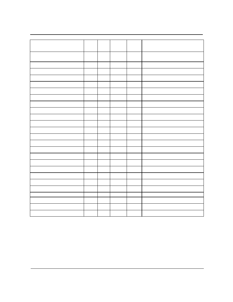
ZL20200
Data Sheet
45
Zarlink Semiconductor Inc.
Notes:
Note 1: All receive currents include all receiver sections plus Rx VHF and UHF PLL's, and UHF LO input buffer circuits. The LO output
buffer and frequency doubler are not included.
Note 2: All transmit currents include all transmit sections plus Tx VHF and UHF PLL's, and UHF LO input buffer circuits. The LO
output buffer and frequency doubler are not included.
Note 3: Includes UHF LO input buffer.
Note 4: This is only applicable in 1900 MHz band.
Note 5: The UHF LO output buffer need only be powered up if required to drive an external circuit, for example, a receive front end
mixer.
Note 6: Input signal FM modulated with 8 kHz deviation by 1 kHz modulating signal. Specification is minimum input level to obtain 12
dB SINAD at FM Output (pin 45) using CCITT filter.
Note 7: Input modulation: 1 kHz modulating signal with 8 kHz deviation. Output level at FM out (pin 45) is set by external components.
See application section for details.
Charge Pump off-state
current
5
nA
Fractional Compensation
88
98
108
�A
Full Scale
UHF Buffers
Load Impedance
200
W
Output Level (900 and 1900)
-11
dBm
Load = 200 ohms
Harmonic Level
-40
dBc
LO1900 Output
Rx and Tx IF Synthesizers
Input Frequency
100
430
MHz
Charge Pump Current
0.9
1
1.1
mA
0.45
0.5
0.55
mA
0.22
0.25
0.28
mA
0.11
0.125
0.14
mA
Charge Pump Output Compliance
0.4
Vcc - 0.4
V
Less than +/-10% variation in Iout
Charge Pump sink/source mismatch
15
%
Charge Pump off-state current
5
nA
Rx LO Oscillator
Frequency
140
430
MHz
Phase Noise
-99
dBc/Hz
Freq = 270 MHz, Offset = 30 kHz
Tx LO Oscillator
Frequency
260
430
MHz
Phase Noise
-99
dBc/Hz
Freq = 360 MHz, Offset = 30 kHz
Characteristics
Min.
Value
Typ
Max.
Units
Comments
ZL20200
Data Sheet
46
Zarlink Semiconductor Inc.
6.0 Typical Performance Curves
6.1 Receive
AMPS Rx. - Icc v Temperature
29
30
31
32
33
34
35
36
37
38
-40
25
85
Temperature �C
mA
Vcc = 2.7V
Vcc = 3.0V
Vcc = 3.3V
IS136 Rx. - Icc v Temperature
27
28
29
30
31
32
33
34
35
-40
25
85
Temperature �C
mA
Vcc = 2.7V
Vcc = 3.0V
Vcc = 3.3V
Rx. Gain v AGC (Vcc)
-20
0
20
40
60
80
100
120
0
1
2
3
AGC Volts
dB
Vcc = 2.7V
Vcc = 3.0V
Vcc = 3.3V
Rx. Gain v AGC (Temperature)
-20
0
20
40
60
80
100
120
0
1
2
3
AGC Volts
dB
T = -40�C
T = 25�C
T = 85�C
ZL20200
Data Sheet
47
Zarlink Semiconductor Inc.
6.2 Transmit
Rx. RSSI
0
0.2
0.4
0.6
0.8
1
1.2
1.4
1.6
-150
-100
-50
0
Input Level dBm
RSSI Voltage
-40�C
25�C
85�C
IS136 Tx. 900 MHz - Icc v AGC (Temperature)
0
20
40
60
80
100
120
140
160
180
0
1
2
3
AGC Volts
Icc mA
-40�C
25�C
85�C
IS136 Tx. 900 MHz - Icc v AGC (Vcc)
0
20
40
60
80
100
120
140
160
180
0
1
2
3
AGC Volts
Icc mA
Vcc = 2.7V
Vcc = 3.0V
Vcc = 3.3V
ZL20200
Data Sheet
48
Zarlink Semiconductor Inc.
IS136 Tx. 1900 MHz - Icc v AGC (Vcc)
0
20
40
60
80
100
120
140
160
0
1
2
3
AGC Volts
Icc mA
Vcc = 2.7V
Vcc = 3.0V
Vcc = 3.3V
IS136 Tx.1900 MHz - Icc v AGC (Temperature)
0
20
40
60
80
100
120
140
160
0
1
2
3
AGC Volts
Icc mA
-40�C
25�C
85�C
IS136 Tx. 900 MHz - Power Out v AGC (Vcc)
-60
-50
-40
-30
-20
-10
0
10
20
0
1
2
3
AGC Volts
dBm
Vcc = 2.7V
Vcc = 3.0V
Vcc = 3.3V
IS136 Tx. 900 MHz - Power Out v AGC (Temp.)
-60
-50
-40
-30
-20
-10
0
10
20
0
1
2
3
AGC Volts
dBm
-40�C
25�C
85�C
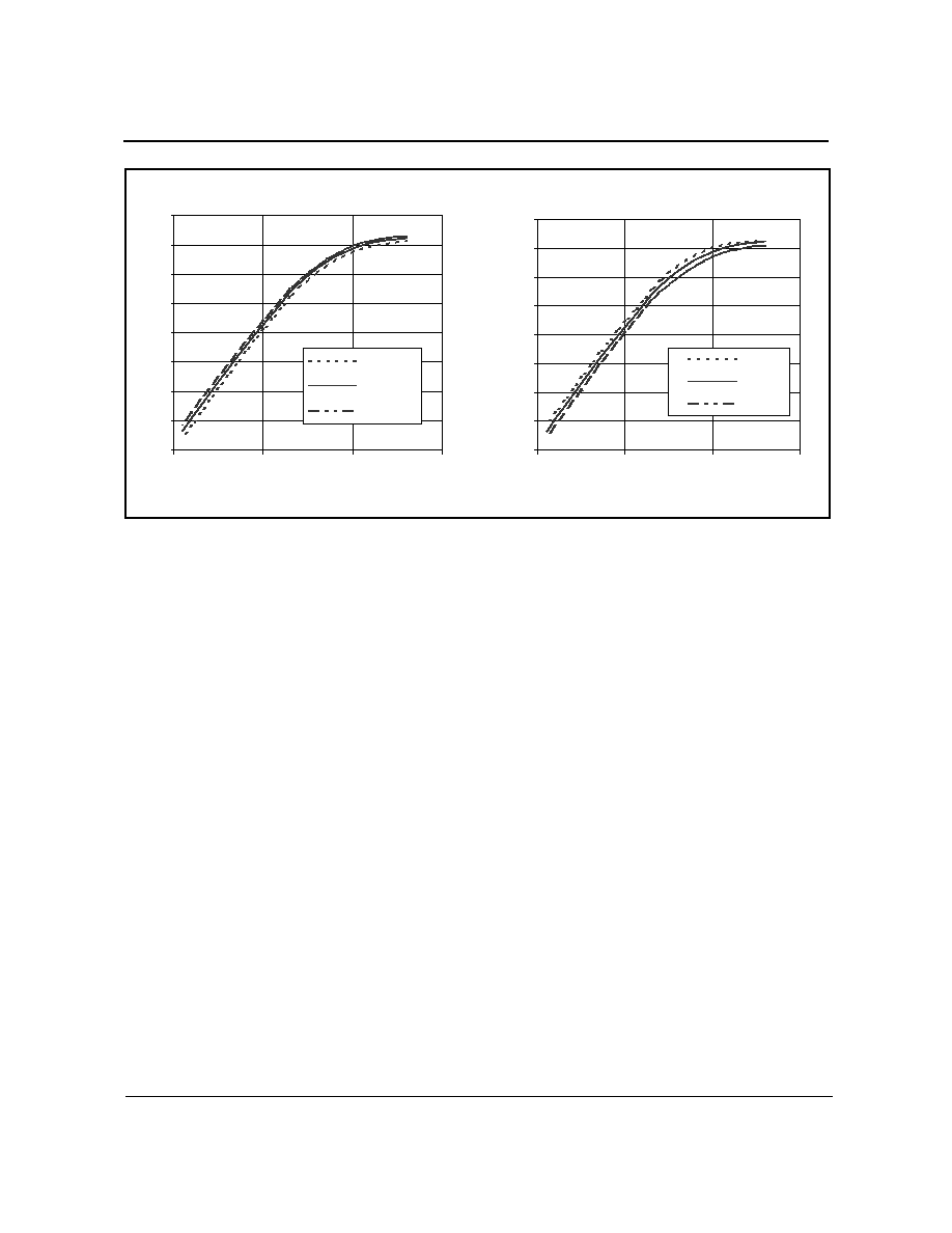
ZL20200
Data Sheet
49
Zarlink Semiconductor Inc.
IS136 Tx. 1900 MHz - Power Out v AGC (Vcc)
-60
-50
-40
-30
-20
-10
0
10
20
0
1
2
3
AGC Volts
dBm
Vcc = 2.7V
Vcc = 3.0V
Vcc = 3.3V
IS136 Tx 1900MHz - Power Out v AGC (Temp.)
-60
-50
-40
-30
-20
-10
0
10
20
0
1
2
3
AGC Volts
dBm
-40�C
25�C
85�C

c Zarlink Semiconductor 2002 All rights reserved.
APPRD.
ISSUE
DATE
ACN
Package Code
Previous package codes
L
1
211130
16Jun01
213841
12Dec02
2


www.zarlink.com
Information relating to products and services furnished herein by Zarlink Semiconductor Inc. or its subsidiaries (collectively "Zarlink") is believed to be reliable.
However, Zarlink assumes no liability for errors that may appear in this publication, or for liability otherwise arising from the application or use of any such
information, product or service or for any infringement of patents or other intellectual property rights owned by third parties which may result from such application or
use. Neither the supply of such information or purchase of product or service conveys any license, either express or implied, under patents or other intellectual
property rights owned by Zarlink or licensed from third parties by Zarlink, whatsoever. Purchasers of products are also hereby notified that the use of product in
certain ways or in combination with Zarlink, or non-Zarlink furnished goods or services may infringe patents or other intellectual property rights owned by Zarlink.
This publication is issued to provide information only and (unless agreed by Zarlink in writing) may not be used, applied or reproduced for any purpose nor form part
of any order or contract nor to be regarded as a representation relating to the products or services concerned. The products, their specifications, services and other
information appearing in this publication are subject to change by Zarlink without notice. No warranty or guarantee express or implied is made regarding the
capability, performance or suitability of any product or service. Information concerning possible methods of use is provided as a guide only and does not constitute
any guarantee that such methods of use will be satisfactory in a specific piece of equipment. It is the user's responsibility to fully determine the performance and
suitability of any equipment using such information and to ensure that any publication or data used is up to date and has not been superseded. Manufacturing does
not necessarily include testing of all functions or parameters. These products are not suitable for use in any medical products whose failure to perform may result in
significant injury or death to the user. All products and materials are sold and services provided subject to Zarlink's conditions of sale which are available on request.
Purchase of Zarlink's I
2
C components conveys a licence under the Philips I
2
C Patent rights to use these components in and I
2
C System, provided that the system
conforms to the I
2
C Standard Specification as defined by Philips.
Zarlink, ZL and the Zarlink Semiconductor logo are trademarks of Zarlink Semiconductor Inc.
Copyright Zarlink Semiconductor Inc. All Rights Reserved.
TECHNICAL DOCUMENTATION - NOT FOR RESALE
For more information about all Zarlink products
visit our Web Site at