 | –≠–ª–µ–∫—Ç—Ä–æ–Ω–Ω—ã–π –∫–æ–º–ø–æ–Ω–µ–Ω—Ç: ZL30119 | –°–∫–∞—á–∞—Ç—å:  PDF PDF  ZIP ZIP |
Document Outline
- Features
- Applications
- Figure 1 - Block Diagram
- Pin Description
- 1.0 Functional Description
- 1.1 DPLL Features
- Table 1 - DPLL1 and DPLL2 Features
- 1.2 DPLL Mode Control
- Figure 2 - Automatic Mode State Machine
- Free-run
- Lock Acquisition
- Normal (locked)
- Holdover
- 1.3 Ref and Sync Inputs
- Figure 3 - Reference and Sync Inputs
- Figure 4 - Output Frame Pulse Alignment
- Table 2 - Set of Pre-Defined Auto-Detect Clock Frequencies
- Table 3 - Set of Pre-Defined Auto-Detect Sync Frequencies
- 1.4 Ref and Sync Monitoring
- Single Cycle Monitor (SCM)
- Coarse Frequency Monitor (CFM)
- Precise Frequency Monitor (PFM)
- Figure 5 - Behaviour of the Guard Soak Timer during CFM or SCM Failures
- 1.5 Output Clocks and Frame Pulses
- Figure 6 - Output Clock Configuration
- Table 4 - Output Clock and Frame Pulse Frequencies
- 1.6 Configurable Input-to-Output and Output-to-Output Delays
- Figure 7 - Phase Delay Adjustments
- 2.0 Software Configuration
- 3.0 References

1
Zarlink Semiconductor Inc.
Zarlink, ZL and the Zarlink Semiconductor logo are trademarks of Zarlink Semiconductor Inc.
Copyright 2005, Zarlink Semiconductor Inc. All Rights Reserved.
A full Design Manual is available to qualified customers.
To register, please send an email to
TimingandSync@Zarlink.com.
Features
∑ Synchronizes with standard telecom system
references and synthesizes a wide variety of
protected telecom line interface clocks that are
compliant with Telcordia GR-253-CORE and ITU-T
G.813
∑ Internal APLL provides standard output clock
frequencies from 6.48 MHz up to 622.08 MHz with
jitter less than 1 ps RMS for OC-48/STM-16
interfaces
∑ Programmable output synthesizers (P0, P1)
generate clock frequencies from any multiple of
8 kHz up to 77.76 MHz in addition to 2 kHz
∑ Provides two DPLLs which are independently
configurable through a serial peripheral interface
∑ DPLL1 provides all the features necessary for
generating SONET/SDH compliant clocks including
automatic hitless reference switching, automatic
mode selection (locked, free-run, holdover), and
selectable loop bandwidth
∑ DPLL2 provides a comprehensive set of features
for generating derived output clocks and other
general purpose clocks
∑ Provides 8 reference inputs which support clock
frequencies with any multiples of 8 kHz up to
77.76 MHz in addition to 2 kHz
∑ Provides 3 sync inputs for output frame pulse
alignment
∑ Generates several styles of output frame pulses
with selectable pulse width, polarity, and frequency
∑ Configurable input to output delay, and output to
output phase alignment
∑ Flexible input reference monitoring automatically
disqualifies references based on frequency and
phase irregularities
∑ Supports IEEE 1149.1 JTAG Boundary Scan
December 2005
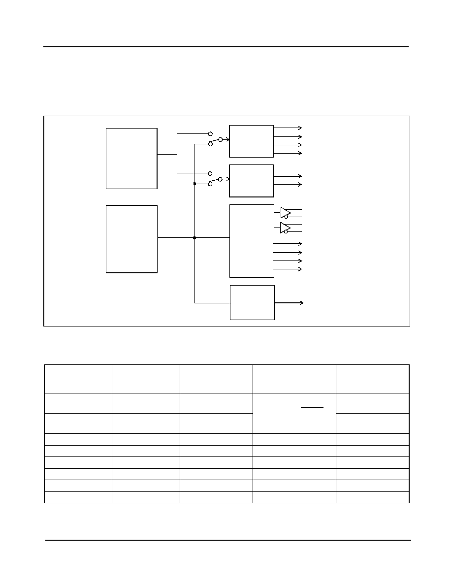
Figure 1 - Block Diagram
dpll1_mod_sel1:0
tck
tdo
tdi tms
trst_b
dpll1_holdover
dpll1_lock
DPLL2
sck
so
si
DPLL1
dpll2_ref
rst_b
dpll1_hs_en
cs_b
diff0_en
diff1_en
Reference
Monitors
ref
sync
ref
ref0
ref1
ref2
ref3
ref4
ref5
ref6
ref7
sync0
sync1
sync2
int_b
sdh_clk0
sdh_clk1
sdh_fp0
sdh_fp1
p0_clk0
p0_clk1
p0_fp0
p0_fp1
p1_clk0
p1_clk1
fb_clk
ref7:0
sync2:0
ref_&_sync_status
Controller &
State Machine
SPI Interface
SONET/SDH
APLL
P0
Synthesizer
P1
Synthesizer
Feedback
Synthesizer
diff0
diff1
IEEE 1449.1
JTAG
Master
Clock
osco
osci
fb_clk/fp
sdh_filter filter_ref0
filter_ref1
ZL30119
SONET/SDH
Low Jitter Line Card Synchronizer
Data Sheet
Ordering Information
ZL30119GGG
100 Pin CABGA
Trays
ZL30119GGG2
100 Pin CABGA*
Trays
*Pb Free Tin/Silver/Copper
-40
o
C to +85
o
C

ZL30119
Data Sheet
2
Zarlink Semiconductor Inc.
Applications
∑ AMCs for AdvancedTCA
TM
and MicroTCA Systems
∑ Multi-Service Edge Switches or Routers
∑ DSLAM Line Cards
∑ WAN Line Cards
∑ RNC/Mobile Switching Center Line Cards
∑ ADM Line Cards

ZL30119
Data Sheet
Table of Contents
3
Zarlink Semiconductor Inc.
1.0 Functional Description . . . . . . . . . . . . . . . . . . . . . . . . . . . . . . . . . . . . . . . . . . . . . . . . . . . . . . . . . . . . . . . . . 11
1.1 DPLL Features . . . . . . . . . . . . . . . . . . . . . . . . . . . . . . . . . . . . . . . . . . . . . . . . . . . . . . . . . . . . . . . . . . . . . 11
1.2 DPLL Mode Control . . . . . . . . . . . . . . . . . . . . . . . . . . . . . . . . . . . . . . . . . . . . . . . . . . . . . . . . . . . . . . . . . . 12
1.3 Ref and Sync Inputs . . . . . . . . . . . . . . . . . . . . . . . . . . . . . . . . . . . . . . . . . . . . . . . . . . . . . . . . . . . . . . . . . 13
1.4 Ref and Sync Monitoring . . . . . . . . . . . . . . . . . . . . . . . . . . . . . . . . . . . . . . . . . . . . . . . . . . . . . . . . . . . . . . 14
1.5 Output Clocks and Frame Pulses . . . . . . . . . . . . . . . . . . . . . . . . . . . . . . . . . . . . . . . . . . . . . . . . . . . . . . . 15
1.6 Configurable Input-to-Output and Output-to-Output Delays . . . . . . . . . . . . . . . . . . . . . . . . . . . . . . . . . . . 17
2.0 Software Configuration . . . . . . . . . . . . . . . . . . . . . . . . . . . . . . . . . . . . . . . . . . . . . . . . . . . . . . . . . . . . . . . . . 18
3.0 References . . . . . . . . . . . . . . . . . . . . . . . . . . . . . . . . . . . . . . . . . . . . . . . . . . . . . . . . . . . . . . . . . . . . . . . . . . . 25

ZL30119
Data Sheet
List of Figures
4
Zarlink Semiconductor Inc.
Figure 1 - Block Diagram . . . . . . . . . . . . . . . . . . . . . . . . . . . . . . . . . . . . . . . . . . . . . . . . . . . . . . . . . . . . . . . . . . . . . 1
Figure 2 - Automatic Mode State Machine . . . . . . . . . . . . . . . . . . . . . . . . . . . . . . . . . . . . . . . . . . . . . . . . . . . . . . . 12
Figure 3 - Reference and Sync Inputs . . . . . . . . . . . . . . . . . . . . . . . . . . . . . . . . . . . . . . . . . . . . . . . . . . . . . . . . . . 13
Figure 4 - Output Frame Pulse Alignment . . . . . . . . . . . . . . . . . . . . . . . . . . . . . . . . . . . . . . . . . . . . . . . . . . . . . . . 13
Figure 5 - Behaviour of the Guard Soak Timer during CFM or SCM Failures . . . . . . . . . . . . . . . . . . . . . . . . . . . . 15
Figure 6 - Output Clock Configuration . . . . . . . . . . . . . . . . . . . . . . . . . . . . . . . . . . . . . . . . . . . . . . . . . . . . . . . . . . 16
Figure 7 - Phase Delay Adjustments . . . . . . . . . . . . . . . . . . . . . . . . . . . . . . . . . . . . . . . . . . . . . . . . . . . . . . . . . . . 17

ZL30119
Data Sheet
List of Tables
5
Zarlink Semiconductor Inc.
Table 1 - DPLL1 and DPLL2 Features . . . . . . . . . . . . . . . . . . . . . . . . . . . . . . . . . . . . . . . . . . . . . . . . . . . . . . . . . . 11
Table 2 - Set of Pre-Defined Auto-Detect Clock Frequencies . . . . . . . . . . . . . . . . . . . . . . . . . . . . . . . . . . . . . . . . 14
Table 3 - Set of Pre-Defined Auto-Detect Sync Frequencies . . . . . . . . . . . . . . . . . . . . . . . . . . . . . . . . . . . . . . . . . 14
Table 4 - Output Clock and Frame Pulse Frequencies . . . . . . . . . . . . . . . . . . . . . . . . . . . . . . . . . . . . . . . . . . . . . 16
Table 5 - Register Map. . . . . . . . . . . . . . . . . . . . . . . . . . . . . . . . . . . . . . . . . . . . . . . . . . . . . . . . . . . . . . . . . . . . . . 18

ZL30119
Data Sheet
6
Zarlink Semiconductor Inc.
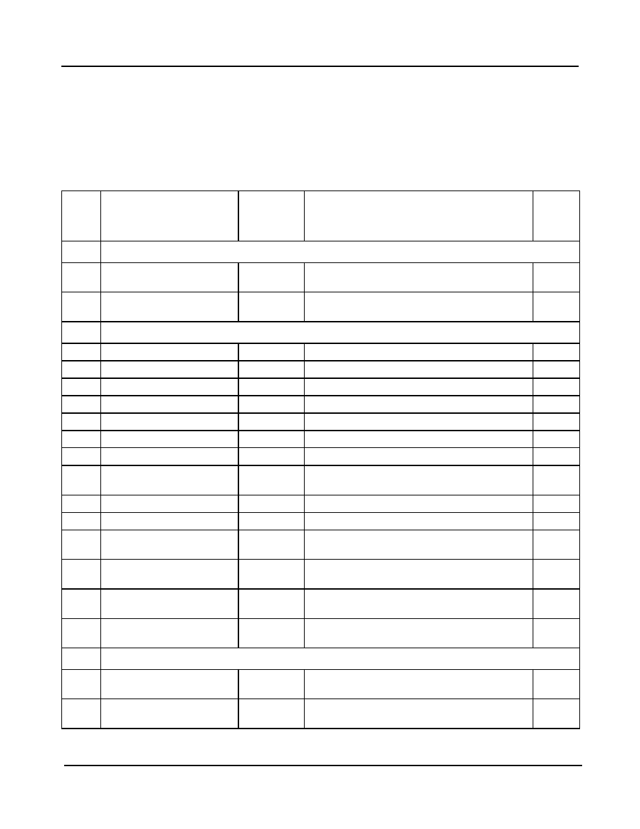
Pin Description
Pin #
Name
I/O
Type
Description
Input Reference
C1
B2
A3
C3
B3
B4
C4
A4
ref0
ref1
ref2
ref3
ref4
ref5
ref6
ref7
I
d
Input References (LVCMOS, Schmitt Trigger). These are input references
available to both DPLL1 and DPLL2 for synchronizing output clocks. All eight
input references can be automatically or manually selected using software
registers. These pins are internally pulled down to Vss.
B1
A1
A2
sync0
sync1
sync2
I
d
Frame Pulse Synchronization References (LVCMOS, Schmitt Trigger).
These are the frame pulse synchronization inputs associated with input
references 0, 1 and 2. These inputs accept frame pulses in a clock format (50%
duty cycle) or a basic frame pulse format with minimum pulse width of 5 ns.
These pins are internally pulled down to V
ss.
Output Clocks and Frame Pulses
D10
sdh_clk0
O
SONET/SDH Output Clock 0 (LVCMOS). This output can be configured to
provide any one of the SONET/SDH clock outputs up to 77.76 MHz. The default
frequency for this output is 77.76 MHz.
G10
sdh_clk1
O
SONET/SDH Output Clock 1 (LVCMOS). This output can be configured to
provide any one of the SONET/SDH clock outputs up to 77.76 MHz. The default
frequency for this output is 19.44 MHz.
E10
sdh_fp0
O
SONET/SDH Output Frame Pulse 0 (LVCMOS). This output can be configured
to provide virtually any style of output frame pulse synchronized with an
associated SONET/SDH family output clock. The default frequency for this frame
pulse output is 8 kHz.
F10
sdh_fp1
O
SONET/SDH Output Frame Pulse 1 (LVCMOS). This output can be configured
to provide virtually any style of output frame pulse synchronized with an
associated SONET/SDH family output clock. The default frequency for this frame
pulse output is 2 kHz.
K9
p0_clk0
O
Programmable Synthesizer 0 - Output Clock 0 (LVCMOS). This output can be
configured to provide any frequency with a multiple of 8 kHz up to 77.76 MHz in
addition to 2 kHz. The default frequency for this output is 2.048 MHz.
K7
p0_clk1
O
Programmable Synthesizer 0 - Output Clock 1 (LVCMOS). This is a
programmable clock output configurable as a multiple or division of the p0_clk0
frequency within the range of 2 kHz to 77.76 MHz. The default frequency for this
output is 8.192 MHz.
K8
p0_fp0
O
Programmable Synthesizer 0 - Output Frame Pulse 0 (LVCMOS). This output
can be configured to provide virtually any style of output frame pulse associated
with the p0 clocks. The default frequency for this frame pulse output is 8 kHz.
J7
p0_fp1
O
Programmable Synthesizer 0 - Output Frame Pulse 1 (LVCMOS). This output
can be configured to provide virtually any style of output frame pulse associated
with the p0 clocks. The default frequency for this frame pulse output is 8 kHz.
ZL30119
Data Sheet
7
Zarlink Semiconductor Inc.
J10
p1_clk0
O
Programmable Synthesizer 1 - Output Clock 0 (LVCMOS). This output can be
configured to provide any frequency with a multiple of 8 kHz up to 77.76 MHz in
addition to 2 kHz. The default frequency for this output is 1.544 MHz (DS1).
K10
p1_clk1
O
Programmable Synthesizer1 - Output Clock 1 (LVCMOS). This is a
programmable clock output configurable as a multiple or division of the p1_clk0
frequency within the range of 2 kHz to 77.76 MHz. The default frequency for this
output is 3.088 MHz (2x DS1).
H10
fb_clk
O
Feedback Clock (LVCMOS). This output is a buffered copy of the feedback
clock for DPLL1. The frequency of this output always equals the frequency of the
selected reference.
E1
dpll2_ref
O
DPLL2 Selected Output Reference (LVCMOS). This is a buffered copy of the
output of the reference selector for DPLL2. Switching between input reference
clocks at this output is not hitless.
A9
B10
diff0_p
diff0_n
O
Differential Output Clock 0 (LVPECL). This output can be configured to provide
any one of the available SDH clocks. The default frequency for this clock output
is 155.52 MHz.
A10
B9
diff1_p
diff1_n
O
Differential Output Clock 1 (LVPECL). This output can be configured to provide
any one of the available SDH clocks. The default frequency for this clock output
is 622.08 MHz clock.
Control
H5
rst_b
I
Reset (LVCMOS, Schmitt Trigger). A logic low at this input resets the device. To
ensure proper operation, the device must be reset after power-up. Reset should
be asserted for a minimum of 300 ns.
J5
dpll1_hs_en
I
u
DPLL1 Hitless Switching Enable (LVCMOS, Schmitt Trigger). A logic high at
this input enables hitless reference switching. A logic low disables hitless
reference switching and re-aligns DPLL1's output phase to the phase of the
selected reference input. This feature can also be controlled through software
registers. This pin is internally pull up to Vdd.
C2
D2
dpll1_mod_sel0
dpll1_mod_sel1
I
u
DPLL1 Mode Select 1:0 (LVCMOS, Schmitt Trigger). During reset, the levels
on these pins determine the default mode of operation for DPLL1 (Automatic,
Normal, Holdover or Freerun). After reset, the mode of operation can be
controlled directly with these pins, or by accessing the dpll1_modesel register
through the serial interface. This pin is internally pull up to Vdd.
K1
diff0_en
I
u
Differential Output 0 Enable (LVCMOS, Schmitt Trigger). When set high, the
differential LVPECL output 0 driver is enabled. When set low, the differential
driver is tristated reducing power consumption. This pin is internally pull up to
Vdd.
D3
diff1_en
I
u
Differential Output 1 Enable (LVCMOS, Schmitt Trigger). When set high, the
differential LVPECL output 1 driver is enabled. When set low, the differential
driver is tristated reducing power consumption.This pin is internally pull up to
Vdd.
Pin #
Name
I/O
Type
Description
ZL30119
Data Sheet
8
Zarlink Semiconductor Inc.
Status
H1
dpll1_lock
O
Lock Indicator (LVCMOS). This is the lock indicator pin for DPLL1. This output
goes high when DPLL1's output is frequency and phase locked to the input
reference.
J1
dpll1_holdover
O
Holdover Indicator (LVCMOS). This pin goes high when DPLL1 enters the
holdover mode.
Serial Interface
E2
sck
I
Clock for Serial Interface (LVCMOS). Serial interface clock.
F1
si
I
Serial Interface Input (LVCMOS). Serial interface data input pin.
G1
so
O
Serial Interface Output (LVCMOS). Serial interface data output pin.
E3
cs_b
I
u
Chip Select for Serial Interface (LVCMOS). Serial interface chip select. This
pin is internally pull up to Vdd.
G2
int_b
O
Interrupt Pin (LVCMOS). Indicates a change of device status prompting the
processor to read the enabled interrupt service registers (ISR). This pin is an
open drain, active low and requires an external pull up to VDD.
APLL Loop Filter
A6
sdh_filter
A
External Analog PLL Loop Filter terminal.
B6
filter_ref0
A
Analog PLL External Loop Filter Reference.
C6
filter_ref1
A
Analog PLL External Loop Filter Reference.
JTAG and Test
J4
tdo
O
Test Serial Data Out (Output). JTAG serial data is output on this pin on the
falling edge of tck. This pin is held in high impedance state when JTAG scan is
not enabled.
K2
tdi
I
u
Test Serial Data In (Input). JTAG serial test instructions and data are shifted in
on this pin. This pin is internally pull up to Vdd. If this pin is not used then it
should be left unconnected.
H4
trst_b
I
u
Test Reset (LVCMOS). Asynchronously initializes the JTAG TAP controller by
putting it in the Test-Logic-Reset state. This pin should be pulsed low on power-
up to ensure that the device is in the normal functional state. This pin is internally
pulled up to Vdd. If this pin is not used then it should be connected to GND.
K3
tck
I
Test Clock (LVCMOS): Provides the clock to the JTAG test logic. If this pin is not
used then it should be pulled down to GND.
J3
tms
I
u
Test Mode Select (LVCMOS). JTAG signal that controls the state transitions of
the TAP controller. This pin is internally pulled up to V
DD
. If this pin is not used
then it should be left unconnected.
Pin #
Name
I/O
Type
Description

ZL30119
Data Sheet
9
Zarlink Semiconductor Inc.
Master Clock
K4
osci
I
Oscillator Master Clock Input (LVCMOS). This input accepts a 20 MHz
reference from a clock oscillator (TCXO, OCXO). The stability and accuracy of
the clock at this input determines the free-run accuracy and the long term
holdover stability of the output clocks.
K5
osco
O
Oscillator Master Clock Output (LVCMOS). This pin must be left unconnected
when the osci pin is connected to a clock oscillator.
Miscellaneous
B5
NC
No Connection. Leave unconnected.
C5
IC
No Connection. Leave unconnected.
D1
IC
No Connection. Leave unconnected.
J2
IC
Internal Connection. Connect to ground.
J6
IC
Internal Connection. Connect to ground.
G3
IC
No Connection. Leave unconnected.
K6
IC
Internal Connection. Leave unconnected.
F2
IC
Internal Connection. Leave unconnected.
F3
IC
Internal Connection. Leave unconnected.
H7 IC
Internal Connection. Connect to ground.
Power and Ground
D9
E4
G8
G9
J8
J9
H6
H8
V
DD
P
P
P
P
P
P
P
P
Positive Supply Voltage. +3.3V
DC
nominal.
E8
F4
V
CORE
P
P
Positive Supply Voltage. +1.8V
DC
nominal.
A5
A8
C10
AV
DD
P
P
P
Positive Analog Supply Voltage. +3.3V
DC
nominal.
B7
B8
H2
AV
CORE
P
P
P
Positive Analog Supply Voltage. +1.8V
DC
nominal.
Pin #
Name
I/O
Type
Description

ZL30119
Data Sheet
10
Zarlink Semiconductor Inc.
I -
Input
I
d
-
Input, Internally pulled down
I
u
-
Input, Internally pulled up
O -
Output
A -
Analog
P -
Power
G -
Ground
D4
D5
D6
D7
E5
E6
E7
F5
F6
F7
G4
G5
G6
G7
E9
F8
F9
H9
V
SS
G
G
G
G
G
G
G
G
G
G
G
G
G
G
G
G
G
G
Ground. 0 Volts.
A7
C7
C8
C9
D8
H3
AV
SS
G
G
G
G
G
G
Analog Ground. 0 Volts.
Pin #
Name
I/O
Type
Description

ZL30119
Data Sheet
11
Zarlink Semiconductor Inc.
1.0 Functional Description
The ZL30119 SONET/SDH Line Card Synchronizer is a highly integrated device that provides timing and
synchronization for network interface cards. It incorporates two independent DPLLs, each capable of locking to one
of eight input references and provides a wide variety of synchronized output clocks and frame pulses.
1.1 DPLL Features
The ZL30119 provides two independently controlled Digital Phase-Locked Loops (DPLL1, DPLL2) for clock and/or
frame pulse synchronization. Table 1 lists the feature summary for both DPLLs.
Feature
DPLL1
DPLL2
Modes of Operation
Free-run, Normal (locked), Holdover
Free-run, Normal (locked), Holdover.
Loop Bandwidth
User selectable: 14 Hz, 28 Hz, or
wideband
1
(890 Hz / 56 Hz / 14 Hz)
1. In the wideband mode, the loop bandwidth depends on the frequency of the reference input. For reference frequencies equal to or
greater than 64 kHz, the loop bandwidth = 890 Hz. For reference frequencies equal to or greater than 8 kHz and less than 64 kHz, the
loop bandwidth = 56 Hz. For reference frequencies equal to 2 kHz, the loop bandwidth is equal to 14 Hz.
Fixed: 14 Hz
Phase Slope Limiting
User selectable: 885 ns/s, 7.5
µs/s,
61
µs/s, or unlimited
User selectable: 61
µs/s, or unlimited
Pull-in Range
Fixed: 130 ppm
Fixed: 130 ppm
Reference Inputs
Ref0 to Ref7
Ref0 to Ref7
Sync Inputs
Sync0, Sync1, Sync2
Sync inputs are not supported.
Input Ref Frequencies
2 kHz, N * 8 kHz up to 77.76 MHz
2 kHz, N * 8 kHz up to 77.76 MHz
Supported Sync Input
Frequencies
166.67 Hz, 400 Hz, 1 kHz, 2 kHz,
8 kHz, 64 kHz.
Sync inputs are not supported.
Input Reference
Selection/Switching
Automatic (based on programmable
priority and revertiveness), or manual
Automatic (based on programmable
priority and revertiveness), or manual
Hitless Ref Switching
Can be enabled or disabled
Can be enabled or disabled
Output Clocks
diff0_p/n, diff1_p/n, sdh_clk0, sdh_clk1,
p0_clk0, p0_clk1, p1_clk0, p1_clk1,
fb_clk.
p0_clk0, p0_clk1, p1_clk0, p1_clk1.
Output Frame Pulses
sdh_fp0, sdh_fp1, p0_fp0, p0_fp1
synchronized to active sync reference.
p0_fp0, p0_fp1 not aligned to sync
reference.
Supported Output Clock
Frequencies
As listed in Table 4
As listed in Table 4 for p0_clk0, p0_clk1,
p1_clk0, p1_clk1
Supported Output
Frame Pulse
Frequencies
As listed in Table 4
As listed in Table 4 for p0_fp0, p0_fp not
aligned to sync reference.
External Pins Status
Indicators
Lock, Holdover
None
Table 1 - DPLL1 and DPLL2 Features

ZL30119
Data Sheet
12
Zarlink Semiconductor Inc.
1.2 DPLL Mode Control
Both DPLL1 and DPLL2 independently support three modes of operation - free-run, normal and holdover. The
mode of operation can be manually set or controlled by an automatic state machine as shown in Figure 2.
Figure 2 - Automatic Mode State Machine
Free-run
The free-run mode occurs immediately after a reset cycle or when the DPLL has never been synchronized to a
reference input. In this mode, the frequency accuracy of the output clocks is equal to the frequency accuracy of the
external master oscillator.
Lock Acquisition
The input references are continuously monitored for frequency accuracy and phase regularity. If at least one of the
input references is qualified by the reference monitors, then the DPLL will begin lock acquisition on that input. Given
a stable reference input, the ZL30119 will enter in the Normal (locked) mode.
Normal (locked)
The usual mode of operation for the DPLL is the normal mode where the DPLL phase locks to a selected qualified
reference input and generates output clocks and frame pulses with a frequency accuracy equal to the frequency
accuracy of the reference input. While in the normal mode, the DPLL's clock and frame pulse outputs comply with
the MTIE and TDEV wander generation specifications as described in Telcordia and ITU-T telecommunication
standards.
Holdover
When the DPLL operating in the normal mode loses its reference input, and no other qualified references are
available, it will enter the holdover mode and continue to generate output clocks based on historical frequency data
collected while the DPLL was synchronized.
Reset
Another reference is
qualified and available
for selection
Phase lock on
the selected
reference is
achieved
Lock
Acquisition
Normal
(Locked)
No references are
qualified and
available for
selection
Free-Run
Holdover
Selected reference
fails
All references are monitored
for frequency accuracy and
phase regularity, and at least
one reference is qualified.
Normal
(Locked)
ZL30119
Data Sheet
13
Zarlink Semiconductor Inc.
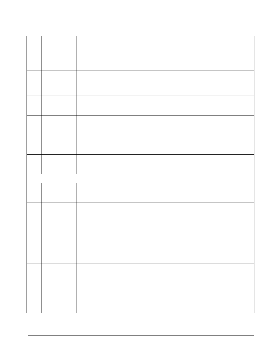
1.3 Ref and Sync Inputs
There are eight reference clock inputs (ref0 to ref7) available to both DPLL1 and DPLL2. The selected reference
input is used to synchronize the output clocks. Each of the DPLLs have independent reference selectors which can
be controlled using a built-in state machine or set in a manual mode.
Figure 3 - Reference and Sync Inputs
In addition to the reference inputs, DPLL1 has three optional frame pulse synchronization inputs (sync0 to sync2)
used to align the output frame pulses. The sync
n
input is selected with its corresponding ref
n
input, where n = 0, 1,
or 2. Note that the sync input cannot be used to synchronize the DPLL, it only determines the alignment of the
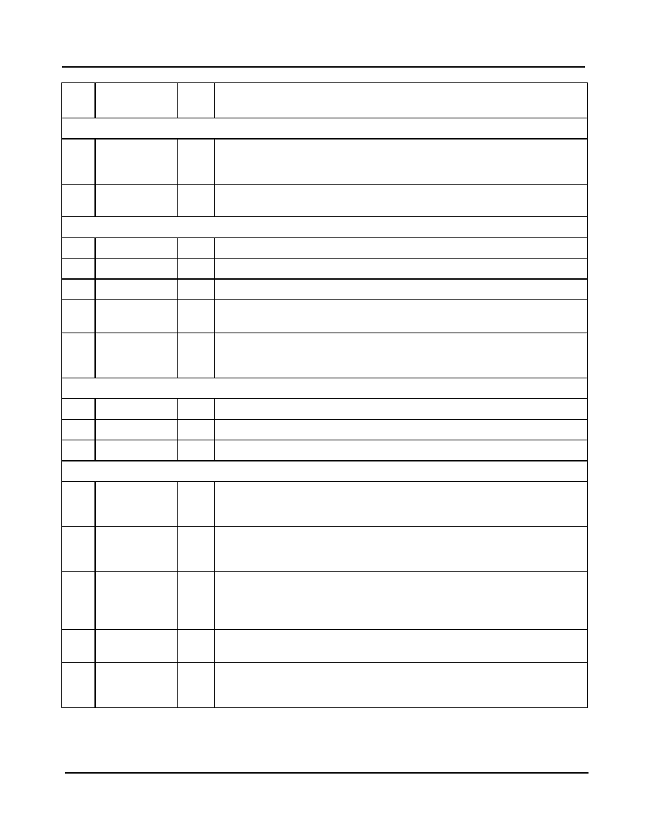
frame pulse outputs. An example of output frame pulse alignment is shown in Figure 4.
Figure 4 - Output Frame Pulse Alignment
ref7:0
sync2:0
DPLL2
DPLL1
ref
n
sdh/p0/p1_clk
x
sdh/p0_fp
x
Without a frame pulse
signal at the sync input,
the output frame pulses
will align to any arbitrary
cycle of its associated
output clock.
sync
n
- no frame pulse signal present
When a frame pulse
signal is present at the
sync input, the DPLL
will align the output
frame pulses to the
output clock edge that is
aligned to the input
frame pulse.
ref
n
sdh/p0/p1_clk
x
sdh/p0_fp
x
sync
n
n = 0, 1, 2
x = 0, 1
n = 0, 1, 2
x = 0, 1
ZL30119
Data Sheet
14
Zarlink Semiconductor Inc.
Each of the ref inputs accept a single-ended LVCMOS clock with a frequency ranging from 2 kHz to 77.76 MHz.
Built-in frequency detection circuitry automatically determines the frequency of the reference if its frequency is
within the set of pre-defined frequencies as shown in Table 2. Custom frequencies definable in multiples of 8 kHz
are also available.
Each of the sync inputs accept a single-ended LVCMOS frame pulse. Since alignment is determined from the rising
edge of the frame pulse, there is no duty cycle restriction on this input, but there is a minimum pulse width
requirement of 5 ns. Frequency detection for the sync inputs is automatic for the supported frame pulse frequencies
shown in Table 3.
1.4 Ref and Sync Monitoring
All input references (ref0 to ref7) are monitored for frequency accuracy and phase regularity. New references are
qualified before they can be selected as a synchronization source, and qualified references are continuously
monitored to ensure that they are suitable for synchronization. The process of qualifying a reference depends on
four levels of monitoring.
Single Cycle Monitor (SCM)
The SCM block measures the period of each reference clock cycle to detect phase irregularities or a missing clock
edge. In general, if the measured period deviates by more than 50% from the nominal period, then an SCM failure
(scm_fail) is declared.
2 kHz
8 kHz
64 kHz
1.544 MHz
2.048 MHz
6.48 MHz
8.192 MHz
16.384 MHz
19.44 MHz
38.88 MHz
77.76 MHz
Custom A
Custom B
Table 2 - Set of Pre-Defined Auto-Detect Clock Frequencies
166.67 Hz
(48x 125
µs frames)
400 Hz
1 kHz
2 kHz
8 kHz
64 kHz
Table 3 - Set of Pre-Defined Auto-Detect Sync Frequencies

ZL30119
Data Sheet
15
Zarlink Semiconductor Inc.
Coarse Frequency Monitor (CFM)
The CFM block monitors the reference frequency over a measurement period of 30
µs so that it can quickly detect
large changes in frequency. A CFM failure (cfm_fail) is triggered when the frequency has changed by more than 3%
or approximately 30000 ppm.
Precise Frequency Monitor (PFM)
The PFM block measures the frequency accuracy of the reference over a 10 second interval. To ensure an
accurate frequency measurement, the PFM measurement interval is re-initiated if phase or frequency irregularities
are detected by the SCM or CFM. The PFM provides a level of hysteresis between the acceptance range and the
rejection range to prevent a failure indication from toggling between valid and invalid for references that are on the
edge of the acceptance range.
When determining the frequency accuracy of the reference input, the PFM uses the external oscillator's output
frequency (f
ocsi
) as its point of reference.
Guard Soak Timer (GST)
The GST block mimics the operation of an analog integrator by accumulating failure events from the CFM and the
SCM blocks and applying a selectable rate of decay when no failures are detected.
As shown in Figure 5, a GST failure (gst_fail) is triggered when the accumulated failures have reached the upper
threshold during the disqualification observation window. When there are no CFM or SCM failures, the accumulator
decrements until it reaches its lower threshold during the qualification window.
Figure 5 - Behaviour of the Guard Soak Timer during CFM or SCM Failures
All sync inputs (sync0 to sync2) are continuously monitored to ensure that there is a correct number of reference
clock cycles within the frame pulse period.
1.5 Output Clocks and Frame Pulses
The ZL30119 offers a wide variety of outputs including two low-jitter differential LVPECL clocks (diff0_p/n,
diff1_p/n), two SONET/SDH LVCMOS (sdh_clk0, sdh_clk1) output clocks and four programmable LVCMOS
(p0_clk0, p0_clk1, p1_clk0, p1_clk1) output clocks. In addition to the clock outputs, two LVCMOS SONET/SDH
frame pulse outputs (sdh_fp0, sdh_fp1) and two LVCMOS programmable frame pulses (p0_fp0, p0_fp1) are also
available.
ref
CFM or SCM failures
upper threshold
lower threshold
t
d
- disqualification time
t
q
- qualification time = n * t
d
t
d
t
q
gst_fail
ZL30119
Data Sheet
16
Zarlink Semiconductor Inc.
The feedback clock (fb_clk) of DPLL1 is available as an output clock. Its output frequency is always equal to
DPLL1's selected input frequency.
The output clocks and frame pulses derived from the SONET/SDH APLL are always synchronous with DPLL1, and
the clocks and frame pulses generated from the programmable synthesizers can be synchronized to either DPLL1
or DPLL2. This allows the ZL30119 to have two independent timing paths.
Figure 6 - Output Clock Configuration
The supported frequencies for the output clocks and frame pulses are shown in Table 4.
diff0_p/n,
diff1_p/n
(LVPECL)
sdh_clk0,
sdh_clk1
(LVCMOS)
p0_clk0, p1_clk0
(LVCMOS)
p0_clk1, p1_clk1
(LVCMOS)
sdh_fp0, shd_fp1,
p0_fp0, p0_fp1
(LVCMOS)
6.48 MHz
6.48 MHz
2 kHz
p
x
_clk0
p
x
_clk1 =
2
M
166.67 Hz
(48x 125
µs frames)
19.44 MHz
9.72 MHz
N * 8 kHz (up to
77.76 MHz)
400 Hz
38.88 MHz
12.96 MHz
1 kHz
51.84 MHz
19.44 MHz
2 kHz
77.76 MHz
25.92 MHz
4 kHz
155.52 MHz
38.88 MHz
8 kHz
311.04 MHz
51.84 MHz
32 kHz
622.08 MHz
77.76 MHz
64 kHz
Table 4 - Output Clock and Frame Pulse Frequencies
DPLL2
p0_clk0
p0_fp0
p0_clk1
p0_fp1
P0
Synthesizer
DPLL1
p1_clk0
p1_clk1
P1
Synthesizer
sdh_clk0
sdh_fp0
sdh_clk1
sdh_fp1
SONET/SDH
APLL
diff0
diff1
Feedback
Synthesizer
fb_clk

ZL30119
Data Sheet
17
Zarlink Semiconductor Inc.
1.6 Configurable Input-to-Output and Output-to-Output Delays
The ZL30119 allows programmable static delay compensation for controlling input-to-output and output-to-output
delays of its clocks and frame pulses.
All of the output synthesizers (SONET/SDH, P0, P1, Feedback) locked to DPLL1 can be configured to lead or lag
the selected input reference clock using the DPLL1 Fine Delay. The delay is programmed in steps of 119.2 ps with
a range of -128 to +127 steps giving a total delay adjustment in the range of -15.26 ns to +15.14 ns. Negative
values delay the output clock, positive values advance the output clock. Synthesizers that are locked to DPLL2 are
unaffected by this delay adjustment.
In addition to the fine delay introduced in the DPLL1 path, the SONET/SDH, P0, and P1 synthesizers have the
ability to add their own fine delay adjustments using the P0 Fine Delay, P1 Fine Delay, and SDH Fine Delay.
These delays are also programmable in steps of 119.2 ps with a range of -128 to +127 steps.
In addition to these delays, the single-ended output clocks of the SONET/SDH, P0, and P1 synthesizers can be
independently offset by 90, 180 and 270 degrees using the Coarse Delay, and the SONET/SDH differential outputs
can be independently delayed by -1.6 ns, 0 ns, +1.6 ns or +3.2 ns using the Diff Delay. The output frame pulses
(SONET/SDH, P0) can be independently offset with respect to each other using the FP Delay.
Figure 7 - Phase Delay Adjustments
DPLL1
DPLL2
P0 Fine Delay
p0_clk0
p0_clk1
p0_fp0
p0_fp1
P0
Synthesizer
Coarse Delay
Coarse Delay
FP Delay
FP Delay
fb_clk
p1_clk0
p1_clk1
P1 Fine Delay
Diff Delay
Diff Delay
diff0
diff1
SONET/SDH
APLL
sdh_clk0
sdh_clk1
sdh_fp0
sdh_fp1
SDH Fine Delay
Feedback
Synthesizer
DPLL1 Fine Delay
Coarse Delay
Coarse Delay
FP Delay
FP Delay
Coarse Delay
Coarse Delay
P1
Synthesizer
ZL30119
Data Sheet
18
Zarlink Semiconductor Inc.
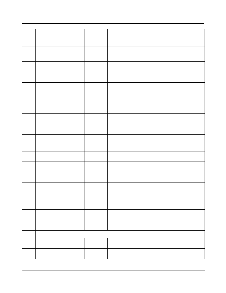
2.0 Software Configuration
The ZL30119 is mainly controlled by accessing software registers through the serial peripheral interface (SPI). The
device can be configured to operate in a highly automated manner which minimizes its interaction with the system's
processor, or it can operate in a manual mode where the system processor controls most of the operation of the
device.
The following table provides a summary of the registers available for status updates and configuration of the device.
.
Addr
(Hex)
Register
Name
Reset
Value
(Hex)
Description
Type
Miscellaneous Registers
00
id_reg
00
Chip and version identification and reset ready
indication register
R
01
use_hw_ctrl
00
Allows some functions of the device to be
controlled by hardware pins
R/W
Interrupts
02
ref_fail_isr
FF
Reference failure interrupt service register
R
03
dpll1_isr
70
DPLL1 interrupt service register
StickR
04
dpll2_isr
00
DPLL2 interrupt service register
StickR
05
ref_mon_fail_0
FF
Ref0 and ref1 failure indications
StickR
06
ref_mon_fail_1
FF
Ref2 and ref3 failure indications.
StickR
07
ref_mon_fail_2
FF
Ref4 and ref5 failure indications
StickR
08
ref_mon_fail_3
FF
Ref6 and ref7 failure indications
StickR
09
ref_fail_isr_mask
00
Reference failure interrupt service register
mask
R/W
0A
dpll1_isr_mask
00
DPLL1 interrupt service register mask
R/W
0B
dpll2_isr_mask
00
DPLL2 interrupt service register mask
R/W
0C
ref_mon_fail_mask_0
FF
Control register to mask each failure indicator
for ref0 and ref1
R/W
0D
ref_mon_fail_mask_1
FF
Control register to mask each failure indicator
for ref2 and ref3
R/W
0E
ref_mon_fail_mask_2
FF
Control register to mask each failure indicator
for ref4 and ref5
R/W
0F
ref_mon_fail_mask_3
FF
Control register to mask each failure indicator
for ref6 and ref7
R/W
Reference Monitor Setup
10
detected_ref_0
FF
Ref0 and ref1 auto-detected frequency value
status register
R
11
detected_ref_1
FF
Ref2 and ref3 auto-detected frequency value
status register
R
Table 5 - Register Map
ZL30119
Data Sheet
19
Zarlink Semiconductor Inc.
12
detected_ref_2
FF
Ref4 and ref5 auto-detected frequency value
status register
R
13
detected_ref_3
FF
Ref6 and ref7 auto-detected frequency value
status register
R
14
detected_sync_0
EE
Sync0 and sync1 auto-detected frequency
value and sync failure status register
R
15
detected_sync_1
0E
Sync2 auto-detected frequency value and sync
valid status register
R
16
oor_ctrl_0
33
Control register for the ref0 and ref1 out of
range limit
R/W
17
oor_ctrl_1
33
Control register for the ref2 and ref3 out of
range limit
R/W
18
oor_ctrl_2
33
Control register for the ref4 and ref5 out of
range limit
R/W
19
oor_ctrl_3
33
Control register for the ref6 and ref7 out of
range limit
R/W
1A
gst_mask_0
FF
Control register to mask the inputs to the guard
soak timer for ref0 to ref3
R/W
1B
gst_mask_1
FF
Control register to mask the inputs to the guard
soak timer for ref4 to ref7
R/W
1C
gst_qualif_time
1A
Control register for the guard_soak_timer
qualification time and disqualification time for
the references
R/W
DPLL1 Control
1D
dpll1_ctrl_0
See
Register
Description
Control register for the DPLL1 filter control;
phase slope limit, bandwidth and hitless
switching
R/W
1E
dpll1_ctrl_1
See
Register
Description
Holdover update time, filter_out_en,
freq_offset_en, revert enable
R/W
1F
dpll1_modesel
See
Register
Description
Control register for the DPLL1 mode of
operation
R/W
20
dpll1_refsel
00
DPLL1 reference selection or reference
selection status
R/W
21
dpll1_ref_fail_mask
3C
Control register to mask each failure indicator
(SCM, CFM, PFM and GST) used for automatic
reference switching and automatic holdover
R/W
22
dpll1_wait_to_restore
00
Control register to indicate the time to restore a
previous failed reference
R/W
Addr
(Hex)
Register
Name
Reset
Value
(Hex)
Description
Type
Table 5 - Register Map (continued)
ZL30119
Data Sheet
20
Zarlink Semiconductor Inc.
23
dpll1_ref_rev_ctrl
00
Control register for the ref0 to ref7 enable
revertive signals
R/W
24
dpll1_ref_pri_ctrl_0
10
Control register for the ref0 and ref1 priority
values
R/W
25
dpll1_ref_pri_ctrl_1
32
Control register for the ref2 and ref3 priority
values
R/W
26
dpll1_ref_pri_ctrl_2
54
Control register for the ref4 and re5 priority
values
R/W
27
dpll1_ref_pri_ctrl_3
76
Control register for the ref6 and ref7 priority
values
R/W
28
dpll1_lock_holdover_status
04
DPLL1 lock and holdover status register
R
29
reserved
03
Leave as default
R/W
DPLL2 Control
2A
dpll2_ctrl_0
00
Control register to program the DPLL2: hitless
switching, the phase slope limit and DPLL
enable
R/W
2B
dpll2_ctrl_1
04
Control register to program the DPLL2:
filter_out_en, freq_offset_en, revert enable
R/W
2C
dpll2_modesel
02
Control register to select the mode of operation
of the DPLL2
R/W
2D
dpll2_refsel
00
DPLL2 reference selection or reference
selection status
R/W
2E
dpll2_ref_fail_mask
3C
Control register to mask each failure indicator
(SCM, CFM, PFM and GST) used for automatic
reference switching and automatic holdover
R/W
2F
dpll2_wait_to_restore
00
Control register to indicate the time to restore a
previous failed reference for the DPLL2 path
R/W
30
dpll2_ref_rev_ctrl
00
Control register for the ref0 to ref7 enable
revertive signals
R/W
31
dpll2_ref_pri_ctrl_0
10
Control register for the ref0 and ref1 priority
values
R/W
32
dpll2_ref_pri_ctrl_1
32
Control register for the ref2 and ref3 priority
values
R/W
33
dpll2_ref_pri_ctrl_2
54
Control register for the ref4 and re5 priority
values
R/W
34
dpll2_ref_pri_ctrl_3
76
Control register for the ref6 and ref7 priority
values
R/W
35
dpll2_lock_holdover_status
04
DPLL2 lock and holdover status register
R
P0 Configuration Registers
Addr
(Hex)
Register
Name
Reset
Value
(Hex)
Description
Type
Table 5 - Register Map (continued)
ZL30119
Data Sheet
21
Zarlink Semiconductor Inc.
36
p0_enable
8F
Control register to enable p0_clk0, p0_clk1,
p0_fp0, p0_fp1, the P0 synthesizer and select
the source
R/W
37
p0_run
0F
Control register to generate p0_clk0, p0_clk1,
p0_fp0 and p0_fp1
R/W
38
p0_freq_0
00
Control register for the [7:0] bits of the N of
N*8k clk0
R/W
39
p0_freq_1
01
Control register for the [13:8] bits of the N of
N*8k clk0
R/W
3A
p0_clk0_offset90
00
Control register for the p0_clk0 phase position
coarse tuning
R/W
3B
p0_clk1_div
3E
Control register for the p0_clk1 frequency
selection
R/W
3C
p0_clk1_offset90
00
Control register for the p0_clk1 phase position
coarse tuning
R/W
3D
p0_offset_fine
00
Control register for the output/output phase
alignment fine tuning for p0 path
R/W
3E
p0_fp0_freq
05
Control register to select the p0_fp0 frame
pulse frequency
R/W
3F
p0_fp0_type
83
Control register to select fp0 type
R/W
40
p0_fp0_offset_0
00
Bits [7:0] of the programmable frame pulse
phase offset in multiples of 1/262.14 MHz
R/W
41
p0_fp0_offset_1
00
Bits [15:8] of the programmable frame pulse
phase offset in multiples of 1/262.14 MHz
R/W
42
p0_fp0_offset_2
00
Bits [21:16] of the programmable frame pulse
phase offset in multiples of 8 kHz cycles
R/W
43
p0_fp1_freq
05
Control register to select p0_fp1 frame pulse
frequency
R/W
44
p0_fp1_type
11
Control register to select fp1 type
R/W
45
p0_fp1_offset_0
00
Bits [7:0] of the programmable frame pulse
phase offset in multiples of 1/262.144 MHz
R/W
46
p0_fp1_offset_1
00
Bits [15:8] of the programmable frame pulse
phase offset in multiples of 1/262.144 MHz
R/W
47
p0_fp1_offset_2
00
Bits [21:16] of the programmable frame pulse
phase offset in multiples of 8 kHz cycles
R/W
P1 Configuration Registers
48
p1_enable
83
Control register to enable p1_clk0, p1_clk1, the
P1 synthesizer and select the source
R/W
49
p1_run
03
Control register to generate enable/disable
p1_clk0 and p1_clk1
R/W
Addr
(Hex)
Register
Name
Reset
Value
(Hex)
Description
Type
Table 5 - Register Map (continued)

ZL30119
Data Sheet
22
Zarlink Semiconductor Inc.
4A
p1_freq_0
C1
Control register for the [7:0] bits of the N of
N*8k clk0
R/W
4B
p1_freq_1
00
Control register for the [13:8] bits of the N of
N*8k clk0
R/W
4C
p1_clk0_offset90
00
Control register for the p1_clk0 phase position
coarse tuning
R/W
4D
p1_clk1_div
3F
Control register for the p1_clk1 frequency
selection
R/W
4E
p1_clk1_offset90
00
Control register for the p1_clk1 phase position
coarse tuning
R/W
4F
p1_offset_fine
00
Control register for the output/output phase
alignrment fine tuning
R/W
SDH Configuration Registers
50
sdh_enable
8F
Control register to enable sdh_clk0, sdh_clk1,
sdh_fp0, sdh_fp1 and the SDH PLL
R/W
51
sdh_run
0F
Control register to generate sdh_clk0,
sdh_clk1, sdh_fp0 and sdh_fp1
R/W
52
sdh_clk_div
42
Control register for the sdh_clk0 and sdh_clk1
frequency selection
R/W
53
sdh_clk0_offset90
00
Control register for the sdh_clk0 phase position
coarse tuning
R/W
54
sdh_clk1_offset90
00
Control register for the sdh_clk1 phase position
coarse tuning
R/W
55
sdh_offset_fine
00
Control register for the output/output phase
alignrment fine tuning for sdh path
R/W
56
sdh_fp0_freq
05
Control register to select the sdh_fp0 frame
pulse frequency
R/W
57
sdh_fp0_type
23
Control register to select fp0 type
R/W
58
sdh_fp0_offset_0
00
Bits [7:0] of the programmable frame pulse
phase offset in multiples of 1/311.04 MHz
R/W
59
sdh_fp0_offset_1
00
Bits [15:8] of the programmable frame pulse
phase offset in multiples of 1/311.04 MHz
R/W
5A
sdh_fp0_offset_2
00
Bits [21:16] of the programmable frame pulse
phase offset in multiples of 8 kHz cycles
R/W
5B
sdh_fp1_freq
03
Control register to select sdh_fp1 frame pulse
frequency
R/W
5C
sdh_fp1_type
03
Control register to select fp1 type
R/W
5D
sdh_fp1_offset_0
00
Bits [7:0] of the programmable frame pulse
phase offset in multiples of 1/311.04 MHz
R/W
Addr
(Hex)
Register
Name
Reset
Value
(Hex)
Description
Type
Table 5 - Register Map (continued)

ZL30119
Data Sheet
23
Zarlink Semiconductor Inc.
5E
sdh_fp1_offset_1
00
Bits [15:8] of the programmable frame pulse
phase offset in multiples of 1/311.04 MHz
R/W
5F
sdh_fp1_offset_2
00
Bits [21:16] of the programmable frame pulse
phase offset in multiples of 8 kHz cycles
R/W
Differential Output Configuration
60
diff_ctrl
A3
Control register to enable diff0, diff1 and
diffout1_high
R/W
61
diff_sel
53
Control register to select the diff0 and diff1
frequencies
R/W
External Feedback Configuration
62
fb_control
81
Control register to enable fb_clk and the FB
PLL, int/ext feedback select
R/W
63
fb_offset_fine
F5
Control register for the output/output phase
alignment fine tuning
R/W
64
reserved
Custom Input Frequencies
65
ref_freq_mode_0
00
Control register to set whether to use auto
detect, CustomA or CustomB for ref0 to ref3
R/W
66
ref_freq_mode_1
00
Control register to set whether to use auto
detect, CustomA or CustomB for ref4 to ref7
R/W
67
custA_mult_0
00
Control register for the [7:0] bits of the custom
configuration A. This is the N integer for the
N*8kHz reference monitoring.
R/W
68
custA_mult_1
00
Control register for the [13:8] bits of the custom
configuration A. This is the N integer for the
N*8kHz reference monitoring.
R/W
69
custA_scm_low
00
Control register for the custom configuration A:
single cycle SCM low limiter
R/W
6A
custA_scm_high
00
Control register for the custom configuration
A: single cycle SCM high limiter
R/W
6B
custA_cfm_low_0
00
Control register for the custom configuration
A: The [7:0] bits of the single cycle CFM low
limit
R/W
6C
custA_cfm_low_1
00
Control register for the custom configuration
A: The [15:0] bits of the single cycle CFM low
limit
R/W
6D
custA_cfm_hi_0
00
Control register for the custom configuration
A: The [7:0] bits of the single cycle CFM high
limit
R/W
Addr
(Hex)
Register
Name
Reset
Value
(Hex)
Description
Type
Table 5 - Register Map (continued)

ZL30119
Data Sheet
24
Zarlink Semiconductor Inc.
6E
custA_cfm_hi_1
00
Control register for the custom configuration
A: The [15:0] bits of the single cycle CFM high
limiter
R/W
6F
custA_cfm_cycle
00
Control register for the custom configuration
A: CFM reference monitoring cycles - 1
R/W
70
custA_div
00
Control register for the custom configuration
A: enable the use of ref_div4 for the CFM and
PFM inputs
R/W
71
custB_mult_0
00
Control register for the [7:0] bits of the custom
configuration B. This is the 8 k integer for the
N*8kHz reference monitoring.
R/W
72
custB_mult_1
00
Control register for the [13:8] bits of the custom
configuration B. This is the 8 k integer for the
N*8kHz reference monitoring.
R/W
73
custB_scm_low
00
Control register for the custom configuration B:
single cycle SCM low limiter
R/W
74
custB_scm_high
00
Control register for the custom configuration
B: single cycle SCM high limiter
R/W
75
custB_cfm_low_0
00
Control register for the custom configuration
B: The [7:0] bits of the single cycle CFM low
limiter.
R/W
76
custB_cfm_low_1
00
Control register for the custom configuration
B: The [15:0] bits of the single cycle CFM low
limiter.
R/W
77
custB_cfm_hi_0
00
Control register for the custom configuration
B: The [7:0] bits of the single cycle CFM high
limiter.
R/W
78
custB_cfm_hi_1
00
Control register for the custom configuration
B: The [15:0] bits of the single cycle CFM high
limiter.
R/W
79
custB_cfm_cycle
00
Control register for the custom configuration
B: CFM reference monitoring cycles - 1
R/W
7A
custB_div
00
Control register for the custom configuration
B: enable the use of ref_div4 for the CFM and
PFM inputs
R/W
7B -
7F
Reserved
Addr
(Hex)
Register
Name
Reset
Value
(Hex)
Description
Type
Table 5 - Register Map (continued)

ZL30119
Data Sheet
25
Zarlink Semiconductor Inc.
3.0 References
AdvancedTCA, ATCA and the AdvancedTCA and ATCA logos are trademarks of the PCI Industrial Computer
Manufacturers Group.
This datasheet provides a summary of the high level features of the ZL30119. Refer to the ZL30119 Design Manual
for a more complete description.

c Zarlink Semiconductor 2005 All rights reserved.
ISSUE
APPRD.
DATE
ACN
Package Code
Previous package codes

www.zarlink.com
Information relating to products and services furnished herein by Zarlink Semiconductor Inc. or its subsidiaries (collectively "Zarlink") is believed to be reliable.
However, Zarlink assumes no liability for errors that may appear in this publication, or for liability otherwise arising from the application or use of any such
information, product or service or for any infringement of patents or other intellectual property rights owned by third parties which may result from such application or
use. Neither the supply of such information or purchase of product or service conveys any license, either express or implied, under patents or other intellectual
property rights owned by Zarlink or licensed from third parties by Zarlink, whatsoever. Purchasers of products are also hereby notified that the use of product in
certain ways or in combination with Zarlink, or non-Zarlink furnished goods or services may infringe patents or other intellectual property rights owned by Zarlink.
This publication is issued to provide information only and (unless agreed by Zarlink in writing) may not be used, applied or reproduced for any purpose nor form part
of any order or contract nor to be regarded as a representation relating to the products or services concerned. The products, their specifications, services and other
information appearing in this publication are subject to change by Zarlink without notice. No warranty or guarantee express or implied is made regarding the
capability, performance or suitability of any product or service. Information concerning possible methods of use is provided as a guide only and does not constitute
any guarantee that such methods of use will be satisfactory in a specific piece of equipment. It is the user's responsibility to fully determine the performance and
suitability of any equipment using such information and to ensure that any publication or data used is up to date and has not been superseded. Manufacturing does
not necessarily include testing of all functions or parameters. These products are not suitable for use in any medical products whose failure to perform may result in
significant injury or death to the user. All products and materials are sold and services provided subject to Zarlink's conditions of sale which are available on request.
Purchase of Zarlink's I
2
C components conveys a licence under the Philips I
2
C Patent rights to use these components in and I
2
C System, provided that the system
conforms to the I
2
C Standard Specification as defined by Philips.
Zarlink, ZL and the Zarlink Semiconductor logo are trademarks of Zarlink Semiconductor Inc.
Copyright Zarlink Semiconductor Inc. All Rights Reserved.
TECHNICAL DOCUMENTATION - NOT FOR RESALE
For more information about all Zarlink products
visit our Web Site at