1
Zarlink Semiconductor Inc.
Zarlink, ZL and the Zarlink Semiconductor logo are trademarks of Zarlink Semiconductor Inc.
Copyright 2006, Zarlink Semiconductor Inc. All Rights Reserved.
A full Design Manual is available to qualified customers.
To register, please send an email to
TimingandSync@Zarlink.com.
Features
∑ Synchronizes with standard telecom system
references and synthesizes a wide variety of
protected telecom line interface clocks that are
compliant with Telcordia GR-1244-CORE, GR-253-
CORE, ITU-T G.813, and compatible with ITU-T
G.8261 (formerly G.pactiming)
∑ Internal low jitter APLL provides SONET/SDH
clocks including 6.48 MHz, 19.44 MHz, 38.88 MHz,
51.84 MHz and 77.76 MHz, or 25 MHz and 50 MHz
Synchronous Ethernet output clocks
∑ Programmable output synthesizers (P0, P1)
generate general purpose clock frequencies from
any multiple of 8 kHz up to 100 MHz
∑ Jitter performance of <8 ps RMS on the low jitter
APLL outputs, and <20 ps RMS on the
programmable synthesizer outputs.
∑ Provides 8 reference inputs which support clock
frequencies with any multiples of 8 kHz up to
77.76 MHz in addition to 2 kHz
∑ Provides two DPLLs which have independent
modes of operation (locked, free-run, holdover)
and optional hitless reference switching.
∑ Flexible input reference monitoring automatically
disqualifies references based on frequency and
phase irregularities
∑ Provides 3 sync inputs for output frame pulse
alignment
∑ Generates several styles of output frame pulses
with selectable pulse width, polarity, and frequency
∑ Configurable input to output delay, and output to
output phase alignment
∑ Supports IEEE 1149.1 JTAG Boundary Scan
May 2006
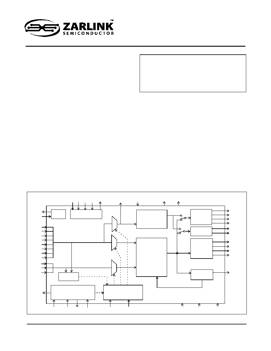
Figure 1 - Block Diagram
dpll1_mod_sel1:0
tck
tdo
tdi tms
trst_b
dpll1_holdover
dpll1_lock
DPLL2
sck
so
si
DPLL1
dpll2_ref
rst_b
dpll1_hs_en
cs_b
Reference
Monitors
ref
sync
ref
ref0
ref1
ref2
ref3
ref4
ref5
ref6
ref7
sync0
sync1
sync2
int_b
apll_clk0
apll_clk1
apll_fp0
apll_fp1
p0_clk0
p0_clk1
p0_fp0
p0_fp1
p1_clk0
p1_clk1
fb_clk
ref7:0
sync2:0
ref_&_sync_status
Controller &
State Machine
SPI Interface
Low Jitter
APLL
P0
Synthesizer
P1
Synthesizer
Feedback
Synthesizer
IEEE 1449.1
JTAG
Master
Clock
osco
osci
fb_clk/fp
apll_filter
filter_ref0
filter_ref1
ZL30120
SONET/SDH/Ethernet
Multi-Rate Line Card Synchronizer
Data Sheet
Ordering Information
ZL30120GGG
100 Pin CABGA
Trays
ZL30120GGG2 100 Pin CABGA**
Trays
**Pb Free Tin/Silver/Copper
-40
o
C to +85
o
C