1
Zarlink Semiconductor Inc.
Zarlink, ZL and the Zarlink Semiconductor logo are trademarks of Zarlink Semiconductor Inc.
Copyright 2003-2004, Zarlink Semiconductor Inc. All Rights Reserved.
Features
� Meets requirements of GR-253 for SONET
Stratum 3 and SONET Minimum Clocks (SMC)
� Meets requirements of GR-1244 for Stratum 3
� Meets requirements of G.813 Option 1 and 2 for
SDH Equipment Clocks (SEC)
� Generates clocks for ST-BUS, DS1, DS2, DS3,
OC-3, E1, E3, STM-1 and 19.44 MHz
� Holdover accuracy of 4x10
-12
meets GR-1244
Stratum 3E and ITU-T G.812 requirements
� Continuously monitors both references for
frequency accuracy exceeding �12 ppm
� Provides "hit-less" reference switching
� Compensates for Master Clock Oscillator
accuracy
� Automatically detects frequency of both reference
clocks and synchronizes to any combination of
8 kHz, 1.544 MHz, 2.048 MHz and 19.44 MHz
reference frequencies
� Allows Hardware or Microprocessor control
� Pin compatible with ZL30410, ZL30402 and
MT90401
Applications
� Synchronization for SDH and SONET Network
Elements
� Clock generation for ST-BUS and GCI backplanes
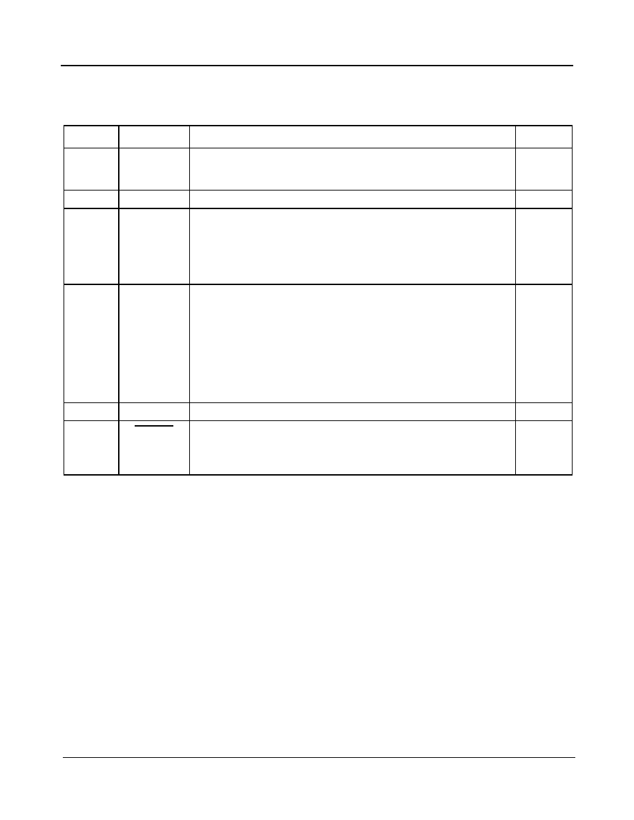
Description
The ZL30407 is a Network Element Phase-Locked
Loop designed to synchronize SDH and SONET
systems. In addition, it generates multiple clocks for
legacy PDH equipment and provides timing for ST-
BUS and GCI backplanes.
November 2004
Ordering Information
Z
L30407QCC
80 Pin LQFP
Trays
ZL30407QCC1
80 Pin LQFP* Trays
*Pb Free Matte Tin
-40
�
C to +85
�
C
ZL30407
SONET/SDH Network Element PLL
Data Sheet
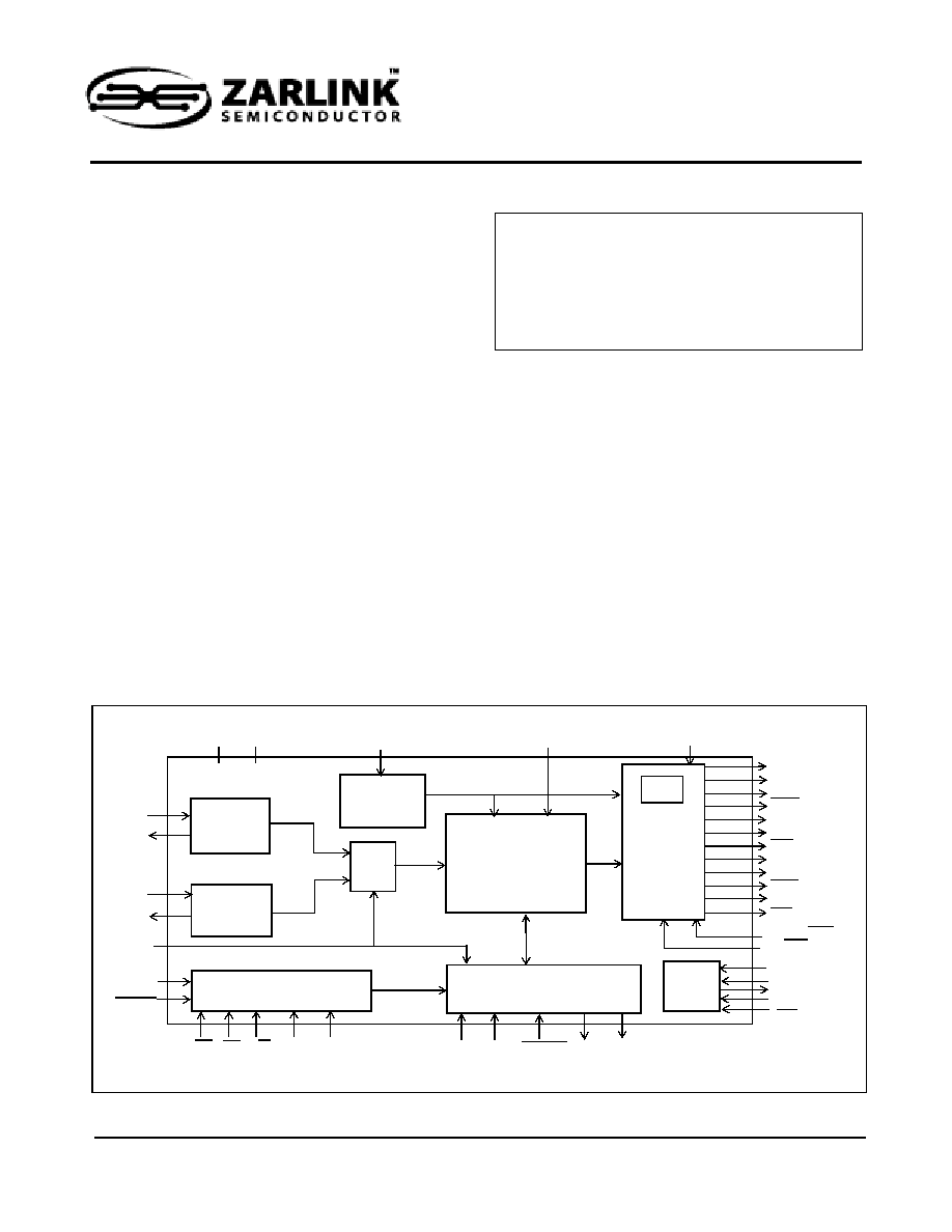
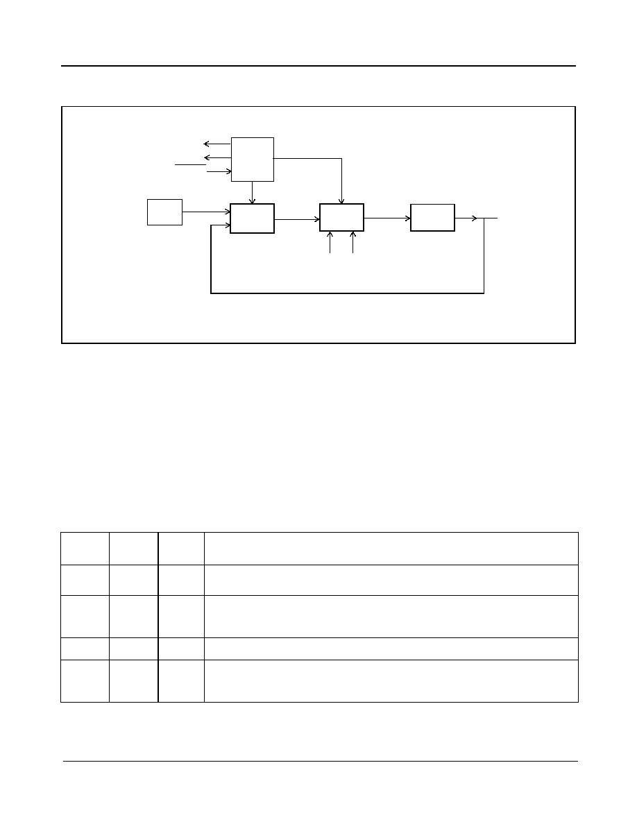
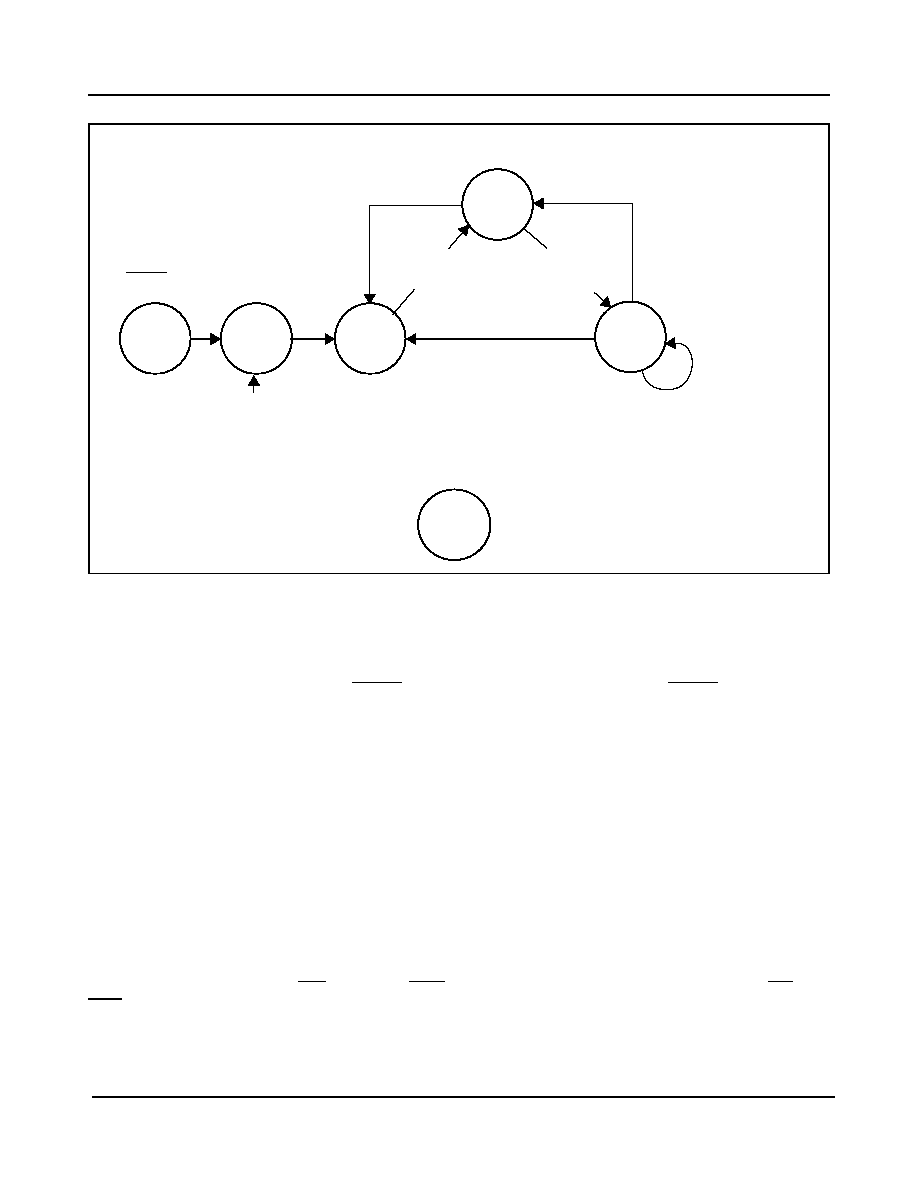
Figure 1 - Functional Block Diagram
Control State Machine
MUX
Microport
Primary
Acquisition
PLL
MS1 MS2
HW
RESET
SEC
Trst
C19o
C34/C44
C16o
C8o
C4o
C2o
C1.5o
F16o
F8o
PRI
C6o
HOLDOVER
LOCK
PRIOR
D0-D7
R/W
CS
C155P/N
E3DS3/OC3
F0o
Secondary
Acquisition
PLL
RefAlign
DS
E3/DS3
JTAG
IEEE
1149.1a
Master Clock
Frequency
Calibration
APLL
SECOR
A0-A6
Tms
Tdo
Tdi
Tclk
Clock
Synthesizer
Core PLL
RefSel
FCS
C20i
VDD GND
OE
R1-17

ZL30407
Data Sheet
2
Zarlink Semiconductor Inc.
The ZL30407 operates in NORMAL (LOCKED), HOLDOVER and FREE-RUN modes to ensure that in the
presence of jitter, wander and interruptions to the reference signals, the generated clocks meet international
standards. The filtering characteristics of the PLL are hardware or software selectable and they do not require any
external adjustable components. The ZL30407 uses an external 20 MHz Master Clock Oscillator to provide a stable
timing source for the HOLDOVER operation.
The ZL30407 operates from a single 3.3 V power supply and offers a 5 V tolerant microprocessor interface.

ZL30407
Data Sheet
Table of Contents
3
Zarlink Semiconductor Inc.
1.0 ZL30407 Pinout . . . . . . . . . . . . . . . . . . . . . . . . . . . . . . . . . . . . . . . . . . . . . . . . . . . . . . . . . . . . . . . . . . . . . . . . 6
1.1 Pin Connections . . . . . . . . . . . . . . . . . . . . . . . . . . . . . . . . . . . . . . . . . . . . . . . . . . . . . . . . . . . . . . . . . . . . . 6
2.0 Functional Description . . . . . . . . . . . . . . . . . . . . . . . . . . . . . . . . . . . . . . . . . . . . . . . . . . . . . . . . . . . . . . . . . 12
2.1 Acquisition PLLs . . . . . . . . . . . . . . . . . . . . . . . . . . . . . . . . . . . . . . . . . . . . . . . . . . . . . . . . . . . . . . . . . . . . 12
2.2 Core PLL . . . . . . . . . . . . . . . . . . . . . . . . . . . . . . . . . . . . . . . . . . . . . . . . . . . . . . . . . . . . . . . . . . . . . . . . . . 12
2.2.1 Digitally Controlled Oscillator (DCO) . . . . . . . . . . . . . . . . . . . . . . . . . . . . . . . . . . . . . . . . . . . . . . . . 13
2.2.2 Filters . . . . . . . . . . . . . . . . . . . . . . . . . . . . . . . . . . . . . . . . . . . . . . . . . . . . . . . . . . . . . . . . . . . . . . . . 13
2.2.3 Phase Slope Limiters . . . . . . . . . . . . . . . . . . . . . . . . . . . . . . . . . . . . . . . . . . . . . . . . . . . . . . . . . . . . 14
2.2.4 Lock Indicator (LOCK) . . . . . . . . . . . . . . . . . . . . . . . . . . . . . . . . . . . . . . . . . . . . . . . . . . . . . . . . . . . 14
2.2.5 Reference Alignment (RefAlign). . . . . . . . . . . . . . . . . . . . . . . . . . . . . . . . . . . . . . . . . . . . . . . . . . . . 14
2.2.5.1 Using RefAlign with 1.544 MHz, 2.048 MHz or 19.44 MHz Reference . . . . . . . . . . . . . . . . . 14
2.2.5.2 Using RefAlign with an 8 kHz Reference . . . . . . . . . . . . . . . . . . . . . . . . . . . . . . . . . . . . . . . . 15
2.3 Clock Synthesizer . . . . . . . . . . . . . . . . . . . . . . . . . . . . . . . . . . . . . . . . . . . . . . . . . . . . . . . . . . . . . . . . . . . 16
2.3.1 Output Clocks. . . . . . . . . . . . . . . . . . . . . . . . . . . . . . . . . . . . . . . . . . . . . . . . . . . . . . . . . . . . . . . . . . 16
2.3.2 Output Clocks Phase Adjustment . . . . . . . . . . . . . . . . . . . . . . . . . . . . . . . . . . . . . . . . . . . . . . . . . . 17
2.4 Control State Machine . . . . . . . . . . . . . . . . . . . . . . . . . . . . . . . . . . . . . . . . . . . . . . . . . . . . . . . . . . . . . . . . 17
2.4.1 Clock Modes . . . . . . . . . . . . . . . . . . . . . . . . . . . . . . . . . . . . . . . . . . . . . . . . . . . . . . . . . . . . . . . . . . 17
2.4.2 ZL30407 State Machine . . . . . . . . . . . . . . . . . . . . . . . . . . . . . . . . . . . . . . . . . . . . . . . . . . . . . . . . . . 17
2.4.2.1 Reset State. . . . . . . . . . . . . . . . . . . . . . . . . . . . . . . . . . . . . . . . . . . . . . . . . . . . . . . . . . . . . . . 18
2.4.2.2 Free-Run State (Free-Run mode) . . . . . . . . . . . . . . . . . . . . . . . . . . . . . . . . . . . . . . . . . . . . . 18
2.4.2.3 Normal State (Normal Mode or Locked Mode). . . . . . . . . . . . . . . . . . . . . . . . . . . . . . . . . . . . 18
2.4.2.4 Holdover State (Holdover Mode) . . . . . . . . . . . . . . . . . . . . . . . . . . . . . . . . . . . . . . . . . . . . . . 19
2.4.2.5 Auto Holdover State . . . . . . . . . . . . . . . . . . . . . . . . . . . . . . . . . . . . . . . . . . . . . . . . . . . . . . . . 19
2.4.3 State Transitions . . . . . . . . . . . . . . . . . . . . . . . . . . . . . . . . . . . . . . . . . . . . . . . . . . . . . . . . . . . . . . . 20
2.5 Master Clock Frequency Calibration Circuit . . . . . . . . . . . . . . . . . . . . . . . . . . . . . . . . . . . . . . . . . . . . . . . 20
2.6 Microprocessor Interface . . . . . . . . . . . . . . . . . . . . . . . . . . . . . . . . . . . . . . . . . . . . . . . . . . . . . . . . . . . . . . 21
2.7 JTAG Interface . . . . . . . . . . . . . . . . . . . . . . . . . . . . . . . . . . . . . . . . . . . . . . . . . . . . . . . . . . . . . . . . . . . . . 21
3.0 Hardware and Software Control . . . . . . . . . . . . . . . . . . . . . . . . . . . . . . . . . . . . . . . . . . . . . . . . . . . . . . . . . . 21
3.1 Hardware Control . . . . . . . . . . . . . . . . . . . . . . . . . . . . . . . . . . . . . . . . . . . . . . . . . . . . . . . . . . . . . . . . . . . 22
3.1.1 Control Pins . . . . . . . . . . . . . . . . . . . . . . . . . . . . . . . . . . . . . . . . . . . . . . . . . . . . . . . . . . . . . . . . . . . 22
3.1.2 Status Pins . . . . . . . . . . . . . . . . . . . . . . . . . . . . . . . . . . . . . . . . . . . . . . . . . . . . . . . . . . . . . . . . . . . . 23
3.2 Software Control . . . . . . . . . . . . . . . . . . . . . . . . . . . . . . . . . . . . . . . . . . . . . . . . . . . . . . . . . . . . . . . . . . . . 23
3.2.1 Control Bits. . . . . . . . . . . . . . . . . . . . . . . . . . . . . . . . . . . . . . . . . . . . . . . . . . . . . . . . . . . . . . . . . . . . 23
3.2.2 ZL30407 Register Map. . . . . . . . . . . . . . . . . . . . . . . . . . . . . . . . . . . . . . . . . . . . . . . . . . . . . . . . . . . 24
4.0 Applications . . . . . . . . . . . . . . . . . . . . . . . . . . . . . . . . . . . . . . . . . . . . . . . . . . . . . . . . . . . . . . . . . . . . . . . . . . 33
4.1 ZL30407 Mode Switching - Examples . . . . . . . . . . . . . . . . . . . . . . . . . . . . . . . . . . . . . . . . . . . . . . . . . . . . 33
4.1.1 System Start-up Sequence: FREE-RUN --> HOLDOVER --> NORMAL . . . . . . . . . . . . . . . . . . . . . 34
4.1.2 Single Reference Operation: NORMAL --> AUTO HOLDOVER --> NORMAL . . . . . . . . . . . . . . . . 35
4.1.3 Single 8 kHz Reference Operation: NORMAL --> AUTO HOLDOVER--> HOLDOVER --> NORMAL
36
4.1.4 Dual Reference Operation: NORMAL --> AUTO HOLDOVER--> HOLDOVER --> NORMAL. . . . . 37
4.2 Master/Slave Timing Protection Switching . . . . . . . . . . . . . . . . . . . . . . . . . . . . . . . . . . . . . . . . . . . . . . . . 39
4.3 Programming Master Clock Oscillator Frequency Calibration Register . . . . . . . . . . . . . . . . . . . . . . . . . . 40
4.4 Power supply filtering . . . . . . . . . . . . . . . . . . . . . . . . . . . . . . . . . . . . . . . . . . . . . . . . . . . . . . . . . . . . . . . . 40
5.0 Characteristics . . . . . . . . . . . . . . . . . . . . . . . . . . . . . . . . . . . . . . . . . . . . . . . . . . . . . . . . . . . . . . . . . . . . . . . . 41
5.1 AC and DC Electrical Characteristics . . . . . . . . . . . . . . . . . . . . . . . . . . . . . . . . . . . . . . . . . . . . . . . . . . . . 41
5.2 Performance Characteristics . . . . . . . . . . . . . . . . . . . . . . . . . . . . . . . . . . . . . . . . . . . . . . . . . . . . . . . . . . . 49

ZL30407
Data Sheet
List of Figures
4
Zarlink Semiconductor Inc.
Figure 1 - Functional Block Diagram . . . . . . . . . . . . . . . . . . . . . . . . . . . . . . . . . . . . . . . . . . . . . . . . . . . . . . . . . . . . 1
Figure 2 - Pin Connections for 80-pin LQFP package . . . . . . . . . . . . . . . . . . . . . . . . . . . . . . . . . . . . . . . . . . . . . . . 6
Figure 3 - Core PLL Functional Block Diagram . . . . . . . . . . . . . . . . . . . . . . . . . . . . . . . . . . . . . . . . . . . . . . . . . . . 13
Figure 4 - C34/C44, C155o Clock Generation Options . . . . . . . . . . . . . . . . . . . . . . . . . . . . . . . . . . . . . . . . . . . . . 17
Figure 5 - ZL30407 State Machine in Software Control configuration . . . . . . . . . . . . . . . . . . . . . . . . . . . . . . . . . . 18
Figure 6 - ZL30407 State Machine in Hardware Control configuration . . . . . . . . . . . . . . . . . . . . . . . . . . . . . . . . . 19
Figure 7 - Hardware and Software Control Options . . . . . . . . . . . . . . . . . . . . . . . . . . . . . . . . . . . . . . . . . . . . . . . . 22
Figure 8 - Primary and Secondary Reference Out of Range Thresholds . . . . . . . . . . . . . . . . . . . . . . . . . . . . . . . 27
Figure 9 - Transition From Free-run to Normal Mode . . . . . . . . . . . . . . . . . . . . . . . . . . . . . . . . . . . . . . . . . . . . . . 34
Figure 10 - Automatic Entry into Auto Holdover State and Recovery into Normal Mode . . . . . . . . . . . . . . . . . . . . 35
Figure 11 - Recovery Procedure From a Single 8 kHz Reference Failure by Transitioning Through the Holdover
State . . . . . . . . . . . . . . . . . . . . . . . . . . . . . . . . . . . . . . . . . . . . . . . . . . . . . . . . . . . . . . . . . . . . . . . . . . . 36
Figure 12 - Entry into Auto Holdover State and Recovery into Normal Mode by Switching References . . . . . . . . 37
Figure 13 - Manual Reference Switching. . . . . . . . . . . . . . . . . . . . . . . . . . . . . . . . . . . . . . . . . . . . . . . . . . . . . . . . 38
Figure 14 - Block Diagram of the Master/Slave Timing Protection Switching . . . . . . . . . . . . . . . . . . . . . . . . . . . . 39
Figure 15 - Power Supply Filtering. . . . . . . . . . . . . . . . . . . . . . . . . . . . . . . . . . . . . . . . . . . . . . . . . . . . . . . . . . . . . 40
Figure 16 - Timing Parameters Measurement Voltage Levels . . . . . . . . . . . . . . . . . . . . . . . . . . . . . . . . . . . . . . . . 42
Figure 17 - Microport Timing . . . . . . . . . . . . . . . . . . . . . . . . . . . . . . . . . . . . . . . . . . . . . . . . . . . . . . . . . . . . . . . . . 43
Figure 18 - ST-BUS and GCI Output Timing . . . . . . . . . . . . . . . . . . . . . . . . . . . . . . . . . . . . . . . . . . . . . . . . . . . . . 44
Figure 19 - DS1 and DS2 Clock Timing . . . . . . . . . . . . . . . . . . . . . . . . . . . . . . . . . . . . . . . . . . . . . . . . . . . . . . . . . 45
Figure 20 - C155o and C19o Timing . . . . . . . . . . . . . . . . . . . . . . . . . . . . . . . . . . . . . . . . . . . . . . . . . . . . . . . . . . . 46
Figure 21 - Input Reference to Output Clock Phase Offset . . . . . . . . . . . . . . . . . . . . . . . . . . . . . . . . . . . . . . . . . . 47
Figure 22 - Input Control Signal Setup and Hold Time . . . . . . . . . . . . . . . . . . . . . . . . . . . . . . . . . . . . . . . . . . . . . 48
Figure 23 - E3 and DS3 Output Timing . . . . . . . . . . . . . . . . . . . . . . . . . . . . . . . . . . . . . . . . . . . . . . . . . . . . . . . . . 48

ZL30407
Data Sheet
List of Tables
5
Zarlink Semiconductor Inc.
Table 1 - Loop Filter Selection . . . . . . . . . . . . . . . . . . . . . . . . . . . . . . . . . . . . . . . . . . . . . . . . . . . . . . . . . . . . . . . . 13
Table 2 - Operating Modes and States. . . . . . . . . . . . . . . . . . . . . . . . . . . . . . . . . . . . . . . . . . . . . . . . . . . . . . . . . . 22
Table 3 - Filter Characteristic Selection . . . . . . . . . . . . . . . . . . . . . . . . . . . . . . . . . . . . . . . . . . . . . . . . . . . . . . . . . 23
Table 4 - Reference Source Select . . . . . . . . . . . . . . . . . . . . . . . . . . . . . . . . . . . . . . . . . . . . . . . . . . . . . . . . . . . . 23
Table 5 - ZL30407 Register Map . . . . . . . . . . . . . . . . . . . . . . . . . . . . . . . . . . . . . . . . . . . . . . . . . . . . . . . . . . . . . . 24
Table 6 - Control Register 1 (R/W). . . . . . . . . . . . . . . . . . . . . . . . . . . . . . . . . . . . . . . . . . . . . . . . . . . . . . . . . . . . . 25
Table 7 - Status Register 1 (R) . . . . . . . . . . . . . . . . . . . . . . . . . . . . . . . . . . . . . . . . . . . . . . . . . . . . . . . . . . . . . . . . 26
Table 8 - Control Register 2 (R/W). . . . . . . . . . . . . . . . . . . . . . . . . . . . . . . . . . . . . . . . . . . . . . . . . . . . . . . . . . . . . 27
Table 9 - Phase Offset Register 2 (R/W) . . . . . . . . . . . . . . . . . . . . . . . . . . . . . . . . . . . . . . . . . . . . . . . . . . . . . . . . 28
Table 10 - Phase Offset Register 1 (R/W) . . . . . . . . . . . . . . . . . . . . . . . . . . . . . . . . . . . . . . . . . . . . . . . . . . . . . . . 28
Table 11 - Device ID Register (R). . . . . . . . . . . . . . . . . . . . . . . . . . . . . . . . . . . . . . . . . . . . . . . . . . . . . . . . . . . . . . 28
Table 12 - Control Register 3 (R/W). . . . . . . . . . . . . . . . . . . . . . . . . . . . . . . . . . . . . . . . . . . . . . . . . . . . . . . . . . . . 29
Table 13 - Clock Disable Register 1 (R/W). . . . . . . . . . . . . . . . . . . . . . . . . . . . . . . . . . . . . . . . . . . . . . . . . . . . . . . 29
Table 14 - Clock Disable Register 2 (R/W). . . . . . . . . . . . . . . . . . . . . . . . . . . . . . . . . . . . . . . . . . . . . . . . . . . . . . . 30
Table 15 - Core PLL Control Register (R/W) . . . . . . . . . . . . . . . . . . . . . . . . . . . . . . . . . . . . . . . . . . . . . . . . . . . . . 30
Table 16 - Fine Phase Offset Register (R/W). . . . . . . . . . . . . . . . . . . . . . . . . . . . . . . . . . . . . . . . . . . . . . . . . . . . . 31
Table 17 - Primary Acquisition PLL Status Register (R). . . . . . . . . . . . . . . . . . . . . . . . . . . . . . . . . . . . . . . . . . . . . 31
Table 18 - Secondary Acquisition PLL Status Register (R) . . . . . . . . . . . . . . . . . . . . . . . . . . . . . . . . . . . . . . . . . . 32
Table 19 - Master Clock Frequency Calibration Register 4 (R/W) . . . . . . . . . . . . . . . . . . . . . . . . . . . . . . . . . . . . . 32
Table 20 - Master Clock Frequency Calibration Register 3 (R/W) . . . . . . . . . . . . . . . . . . . . . . . . . . . . . . . . . . . . . 32
Table 21 - Master Clock Frequency Calibration Register 2 (R/W) . . . . . . . . . . . . . . . . . . . . . . . . . . . . . . . . . . . . . 32
Table 22 - Master Clock Frequency Calibration Register 1 (R/W) . . . . . . . . . . . . . . . . . . . . . . . . . . . . . . . . . . . . . 33
ZL30407
Data Sheet
6
Zarlink Semiconductor Inc.
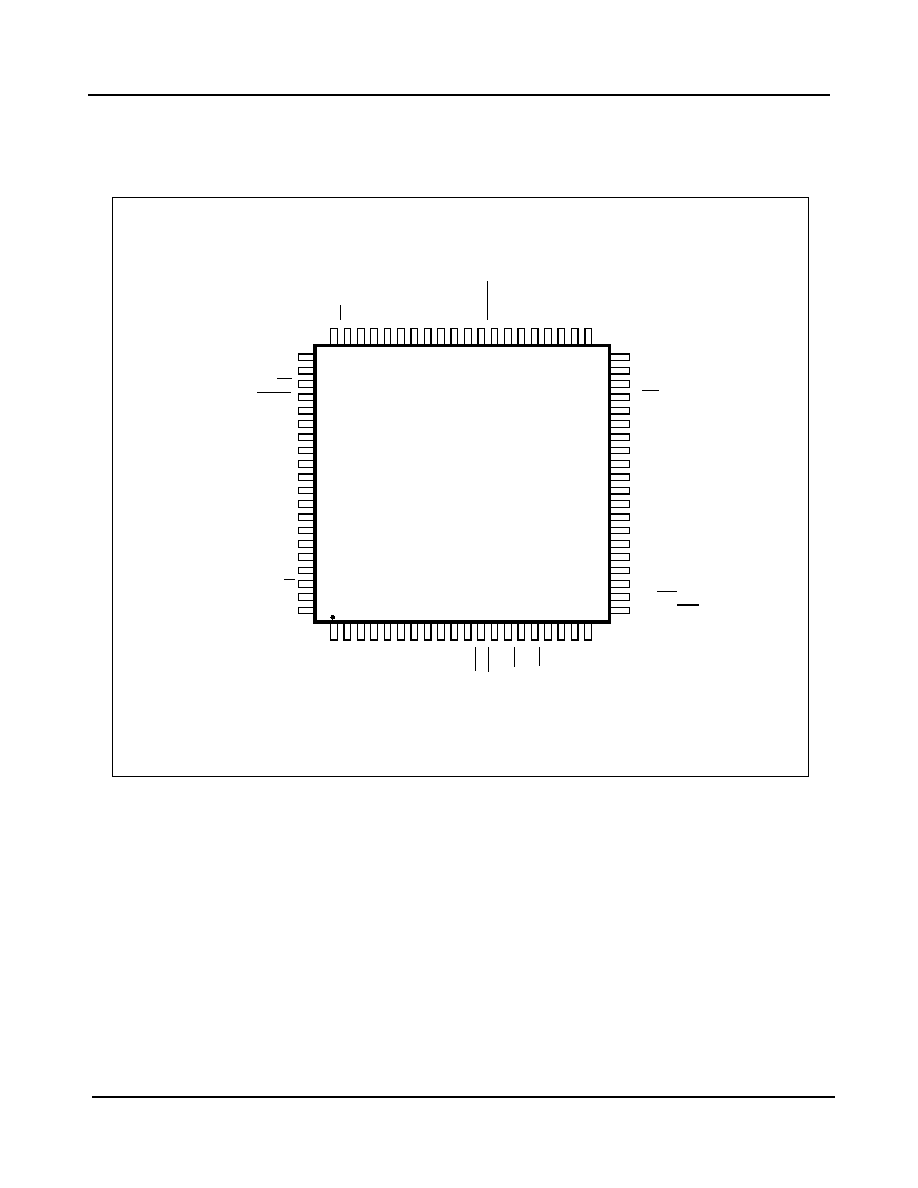
1.0 ZL30407 Pinout
1.1 Pin Connections
Figure 2 - Pin Connections for 80-pin LQFP package
ZL30407
40
42
44
46
48
50
52
54
56
58
60
22
24
26
28
30
34
36
38
32
62
80
78
76
74
72
68
66
64
70
20
18
16
14
12
10
8
6
4
2
Tdi
Tclk
Tms
Tdo
NC
GND
PRI
SEC
E3/DS3
E3DS3/OC3
C155P
C155N
VDD
AVDD
GND
IC
GND
NC
Trst
NC
MS1
A2
A1
C4
o
C8
o
C1
6o
F1
6o
GN
D
VD
D
FC
S
A5
F0
o
C2
o
IC
A3
A4
MS2
GN
D
A6
F8o
SECOR
OE
CS
RESET
HW
D1
D2
D3
GND
IC
D6
R/W
IC
VDD
D4
D5
D7
IC
A0
C1
.
5
o
C1
9o
Re
f
S
el
Re
f
A
lig
n
VD
D
NC
C2
0i
C3
4/
C4
4
GN
D
VD
D
HOL
D
OVER
NC
LO
C
K
NC
DS
IC
PR
I
O
R
GN
D
IC
C6
o
D0
ZL30407
Data Sheet
7
Zarlink Semiconductor Inc.
Pin Description
Pin #
Name
Description
1
IC
Internal Connection. Leave unconnected.
2-5
A1-A4
Address 1 to 4 (5 V tolerant input). Address inputs for the parallel processor
interface. Connect to ground in Hardware Control.
6
GND
Ground. Negative power supply.
7-8
A5-A6
Address 5 to 6 (5 V tolerant input). Address inputs for the parallel processor
interface. Connect to ground in Hardware Control.
9
FCS
Filter Characteristic Select (Input). In Hardware Control, FCS selects the
filtering characteristics of the ZL30407. Set this pin high to have a loop filter
corner frequency of 0.1 Hz and limit the phase slope to 885 ns/sec. Set this pin
low to have corner frequency of 1.5 Hz and limit the phase slope to 41 ns per
1.326 ms. Connect to ground in Software Control. This pin is internally pulled
down to GND.
10
VDD
Positive Power Supply
11
GND
Ground
12
F16o
Frame Pulse ST-BUS 8.192 Mbps (CMOS tristate output). This is an 8 kHz,
61 ns wide, active low framing pulse, which marks beginning of a ST-BUS
frame. This frame pulse is typically used for ST-BUS operation at 8.192 Mbps.
13
C16o
Clock 16.384 MHz (CMOS tristate output). This clock is used for ST-BUS
operation at 8.192 Mbps.
14
C8o
Clock 8.192 MHz (CMOS tristate output). This clock is used for ST-BUS
operation at 8.192 Mbps.
15
C4o
Clock 4.096 MHz (CMOS tristate output). This clock is used for ST-BUS
operation at 2.048 Mbps.
16
C2o
Clock 2.048 MHz (CMOS tristate output). This clock is used for ST-BUS
operation at 2.048 Mbps.
17
F0o
Frame Pulse ST-BUS 2.048 Mbps (CMOS tristate output). This is an 8 kHz,
244ns, active low framing pulse, which marks the beginning of a ST-BUS
frame. This is typically used for ST-BUS operation at 2.048 Mbps and
4.096 Mbps.
18
MS1
Mode Select 1 (Input). The MS1 and MS2 pins select the ZL30407 mode of
operation (Normal, Holdover or Free-run), see Table 2 on page 22 for details.
The logic level at this input is sampled by the rising edge of the F8o frame
pulse. Connect to ground in Software Control.
19
MS2
Mode Select 2 (Input). The MS2 and MS1 pins select the ZL30407 mode of
operation (Normal, Holdover or Free-run), see Table 2 on page 22 for details.
The logic level at this input is sampled by the rising edge of the F8o frame
pulse. Connect to ground in Software Control.
ZL30407
Data Sheet
8
Zarlink Semiconductor Inc.
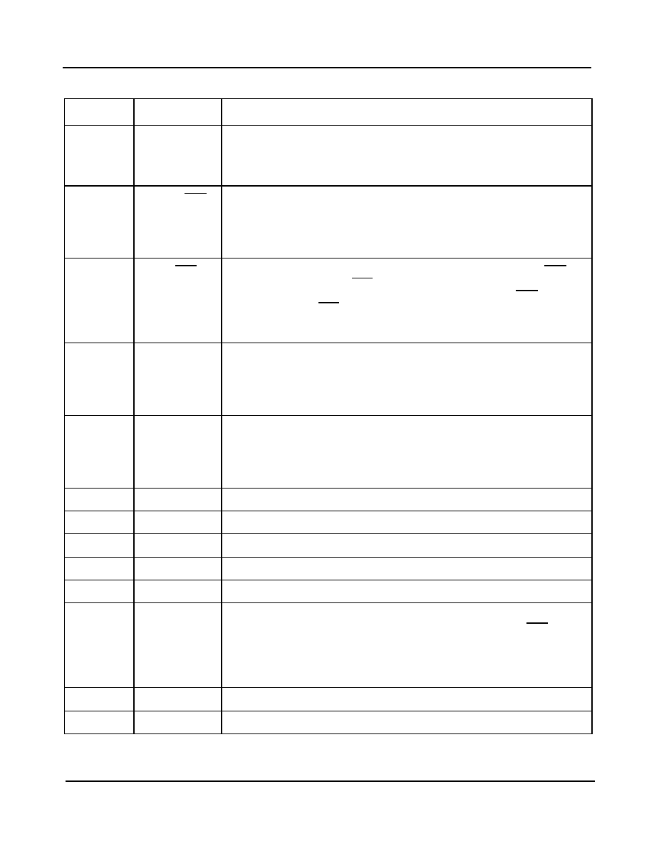
20
F8o
Frame Pulse ST-BUS/GCI 8.192 Mbps (CMOS tristate output). This is an 8
kHz, 122 ns, active high framing pulse, which marks the beginning of a
ST-BUS/GCI frame. This is typically used for ST-BUS/GCI operation at 8.192
Mbps. See Figure 18 for details.
21
E3DS3/OC3
E3DS3 or OC3 Selection (Input). In Hardware Control, a logic low on this pin
enables the C155P/N outputs (pin 30 and pin 31) and sets the C34/C44 output
(pin 53) to provide C8 or C11 clocks. Logic high at this input disables the C155
clock outputs (high impedance) and sets C34/C44 output to provide C34 and
C44 clocks. In Software Control connect this pin to ground.
22
E3/DS3
E3 or DS3 Selection (Input). In Hardware Control, when the E3DS3/OC3 pin
is set high, logic low on E3/DS3 pin selects a 44.736 MHz clock on C34/C44
output and logic high selects 34.368 MHz clock. When E3DS3/OC3 pin is set
low, logic low on E3/DS3 pin selects 11.184 MHz clock on C34/C44 output and
logic high selects 8.592 MHz clock. Connect this input to ground in Software
Control.
23
SEC
Secondary Reference (Input). This input is used as a secondary reference
source for synchronization. The ZL30407 can synchronize to the falling edge
of the 8 kHz, 1.544 MHz or 2.048 MHz clocks and the rising edge of the 19.44
MHz clock. In Hardware Control, selection of the input reference is based upon
the RefSel control input. This pin is internally pulled up to VDD.
24
PRI
Primary Reference (Input). This input is used as a primary reference source
for synchronization. The ZL30407 can synchronize to the falling edge of the 8
kHz, 1.544 MHz or 2.048 MHz clocks and the rising edge of the 19.44 MHz
clock. In Hardware Control, selection of the input reference is based upon the
RefSel control input. This pin is internally pulled up to VDD.
25
GND
Ground
26
IC
Internal Connection. Leave unconnected.
27
GND
Ground
28
AVDD
Positive Analog Power Supply. Connect this pin to VDD.
29
VDD
Positive Power Supply
30
31
C155N
C155P
Clock 155.52 MHz (LVDS output). Differential outputs for the 155.52 MHz
clock. These outputs are enabled by applying logic low to E3DS3/OC3 input or
they can be disabled by applying logic high. In the disabled state the LVDS
outputs are internally terminated with an integrated 100
resistor (two 50
resistors connected in series). The middle point of these resistors is internally
biased from a 1.25 V LVDS bias source.
32
GND
Ground
33
NC
No internal bonding Connection. Leave unconnected.
Pin Description (continued)
Pin #
Name
Description
ZL30407
Data Sheet
9
Zarlink Semiconductor Inc.
34
Tdo
IEEE1149.1a Test Data Output (CMOS output). JTAG serial data is output on
this pin on the falling edge of Tclk clock. If not used, this pin should be left
unconnected.
35
Tms
IEEE1149.1a Test Mode Selection (3.3 V input). JTAG signal that controls the
state transition on the TAP controller. This pin is internally pulled up to VDD. If
not used, this pin should be left unconnected.
36
Tclk
IEEE1149.1a Test Clock Signal (5 V tolerant input). Input clock for the JTAG
test logic. If not used, this pin should be pulled up to VDD.
37
Trst
IEEE1149.1a Reset Signal (3.3 V input). Asynchronous reset for the JTAG
TAP controller. This pin should be pulsed low on power-up to ensure that the
device is in the normal functional state. This pin is internally pulled up to VDD.
If this pin is not used then it should be connected to GND.
38
Tdi
IEEE1149.1a Test Data Input (3.3 V input). Input for JTAG serial test
instructions and data. This pin is internally pulled up to VDD. If not used, this
pin should be left unconnected.
39
NC
No internal bonding Connection. Leave unconnected.
40
NC
No internal bonding Connection. Leave unconnected.
41
PRIOR
Primary Reference Out of Range (Output). Logic high at this pin indicates
that the Primary Reference is off the PLL centre frequency by more than
�
12ppm. These thresholds support Stratum 3 applications. See PRIOR bit
description in Status Register 1 for details.
42
C1.5o
Clock 1.544 MHz (CMOS tristate output). This output provides a 1.544 MHz
DS1 rate clock.
43
C6o
Clock 6.312 MHz (CMOS tristate output). This output provides a 6.312 MHz
DS2 rate clock.
44
IC
Internal Connection. Connect this pin to Ground.
45
GND
Ground
46
C19o
Clock 19.44 MHz (CMOS tristate output). This output provides a 19.44 MHz
clock.
47
RefSel
Reference Source Select (Input). A logic low selects the PRI (primary)
reference source as the input reference signal and logic high selects the SEC
(secondary) input. The logic level at this input is sampled at the rising edge of
F8o. This pin is internally pulled down to GND.
48
RefAlign
Reference Alignment (Input). In Hardware Control pulling this pin low for
250
�
s initiates phase realignment between the input reference and the
generated output clocks. This pin should never be tied low permanently.
Please see Section 2.2.5, Reference Alignment (RefAlign) for more
information. Internally this pin is pulled down to GND.
Pin Description (continued)
Pin #
Name
Description
ZL30407
Data Sheet
10
Zarlink Semiconductor Inc.
49
VDD
Positive Power Supply
50
NC
No internal bonding Connection. Leave unconnected.
51
C20i
Clock 20 MHz (5 V tolerant input). This pin is the input for the 20 MHz Master
Clock Oscillator. The clock oscillator should be connected directly (not AC
coupled) to the C20i input and it must supply clock with duty cycle that is not
worse than 40/60%.
52
GND
Digital Ground
53
C34/C44
Clock 34.368 MHz / clock 44.736 MHz (CMOS Output). This clock is
programmable to be either 34.368 MHz (for E3 applications) or 44.736 MHz
(for DS3 applications) when E3DS3/OC3 is high, or to be either 8.592 MHz or
11.184 MHz when E3DS3/OC3 is low. See description of E3DS3/OC3 and
E3/DS3 inputs for details. In Software Control the functionality of this output is
controlled by Control Register 2 (Table 8 "Control Register 2 (R/W)").
54
VDD
Positive Power Supply
55
HOLDOVER
Holdover Indicator (CMOS output). Logic high at this output indicates that the
device is in Holdover mode.
56
NC
No internal bonding Connection. Leave unconnected.
57
LOCK
Lock Indicator (CMOS output). Logic high at this output indicates that
ZL30407 is locked to the input reference. See LOCK bit description in Status
Register 1 and Section 2.2.4, Lock Indicator (LOCK) for details.
58
NC
No internal bonding Connection. Leave unconnected.
59
DS
Data Strobe (5 V tolerant input). This input is the active low data strobe of the
processor interface.
60
IC
Internal Connection. Connect to ground.
61
SECOR
Secondary Reference Out of Range (Output). Logic high at this pin indicates
that the Secondary Reference is off the PLL centre frequency by more than
�
12 ppm. These thresholds support Stratum 3 applications. See SECOR bit
description in Status Register 1 for details.
62
OE
Output Enable (Input). Logic high on this input enables C19, F16, C16, C8,
C6, C4, C2, C1.5, F8 and F0 signals. Pulling this input low will force the output
clocks pins into a high impedance state.
63
CS
Chip Select (5 V tolerant input). This active low input enables the
microprocessor interface. When CS is set to high, the microprocessor interface
is idle and all Data Bus I/O pins will be in a high impedance state.
Pin Description (continued)
Pin #
Name
Description

ZL30407
Data Sheet
11
Zarlink Semiconductor Inc.
64
RESET
RESET (5 V tolerant input). The ZL30407 must be reset after power-up in
order to set internal registers into a default state. The internal reset is
performed by forcing RESET pin low for a minimum of 1
�
s after the C20
Master Clock is applied to pin C20i. This operation forces the ZL30407 internal
state machine into a RESET state for a duration of 625
�
s.
65
HW
Hardware/Software Control (Input). If this pin it tied low, the ZL30407 is
controlled via the microport. If it is tied high, the ZL30407 is controlled via the
control pins MS1, MS2, FCS, RefSel, RefAlign, E3/DS3 and E3DS3/OC3.
66-69
D0 - D3
Data 0 to Data 3 (5 V tolerant three-state I/O). These ports combined with D4 -
D7 ports form the bi-directional data bus of the microprocessor interface (D0 is
the least significant bit).
70
GND
Ground
71
IC
Internal Connection (Input). Connect this pin to ground.
72
IC
Internal Connection (Input). Connect this pin to ground.
73
VDD
Positive Power Supply
74 - 77
D4 - D7
Data 4 to Data 7 (5 V tolerant three-state I/O). These ports combined with D0 -
D3 ports form the bi-directional data bus of the processor interface (D7 is the
most significant bit).
78
R/W
Read/Write Strobe (5 V tolerant input). This input controls the direction of the
data bus D[0-7] during a microprocessor access. When R/W is high, the
parallel processor is reading data from the ZL30407. When low, the parallel
processor is writing data to the ZL30407.
79
A0
Address 0 (5 V tolerant input). Address input for the microprocessor interface.
A0 is the least significant input.
80
IC
Internal Connection (Input). Connect this pin to ground.
Pin Description (continued)
Pin #
Name
Description

ZL30407
Data Sheet
12
Zarlink Semiconductor Inc.
2.0 Functional Description
The ZL30407 is a Network Element PLL designed to provide timing for SDH and SONET equipment conforming to
ITU-T, ANSI, ETSI and Telcordia recommendations. In addition, it generates clocks for legacy PDH equipment
operating at DS1, DS2, DS3, E1, and E3 rates. The ZL30407 provides clocks for industry standard ST-BUS and
GCI backplanes, and it also supports H.110 timing requirements. The functional block diagram of the ZL30407 is
shown in Figure 1 "Functional Block Diagram" and its operation is described in the following sections.
2.1 Acquisition PLLs
The ZL30407 has two Acquisition PLLs for monitoring the availability and quality of the Primary (PRI) and
Secondary (SEC) reference clocks. Each Acquisition PLL operates independently and locks to the falling edges of
one of the three input reference frequencies: 8 kHz, 1.544 MHz, 2.048 MHz or to the rising edges of 19.44 MHz.
The reference frequency is continuously measured and its current frequency
can be determined from reading the
Acquisition PLL Status Register bits InpFreq1 and InpFreq0 (see Table 17 "Primary Acquisition PLL Status
Register (R)" and Table 18 "Secondary Acquisition PLL Status Register (R)").
The Primary and Secondary Acquisition PLLs are designed to provide status information that identifies two levels of
reference clock quality. For clarity, only the Primary Acquisition PLL is referenced in the text, but the same applies
to the Secondary Acquisition PLL.
� Reference frequency drifts more than
�
12 ppm. In response, the PRIOR (Primary Reference Out of Range)
bit and pin change state to high, in conformance with Stratum 3 requirements defined in GR-1244-CORE.
The PRIOR bit is part of Status Register 1 (Table 7 "Status Register 1 (R)").
� Reference frequency drifted more than
�
30000 ppm or that the reference has been lost completely. In
response, the Primary Acquisition PLL enters its own Holdover mode and indicates this by asserting the
HOLDOVER bit in the Primary Acquisition PLL Status Register (Table 17 "Primary Acquisition PLL Status
Register (R)"). Entry into Holdover forces the Core PLL into the Auto Holdover state.
Outputs of both Acquisition PLLs are connected to a multiplexer (MUX), which allows selection of the desired
reference. This multiplexer channels binary words to the Core PLL digital phase detector (instead of analog signals)
which eliminates quantization errors and improves phase alignment accuracy. The bandwidth of the Acquisition
PLL is much wider than the bandwidth of the following Core PLL. This feature allows cascading Acquisition and
Core PLLs without altering the transfer function of the Core PLL.
2.2 Core PLL
The most critical element of the ZL30407 is its Core PLL, which generates a phase-locked clock, filters jitter and
wander and suppresses input phase transients. All of these features are in agreement with international standards:
� G.813 Option 1 and 2 clocks for SDH equipment
� GR-253 for SONET Stratum 3 and SONET Minimum Clocks (SMC)
� GR-1244 for Stratum 3 Clock
The Core PLL supports three mandatory modes of operation: Free-run, Normal (Locked) and Holdover. Each of
these modes places specific requirements on the building blocks of the Core PLL.
� In Free-run Mode, the Core PLL derives its output clock from the 20 MHz Master Clock Oscillator connected
to pin C20i. The stability of the generated clocks remain the same as the stability of the Master Clock
Oscillator.
� In Normal Mode, the Core PLL locks to one of the Acquisition PLLs. Both Acquisition PLLs provide
preprocessed phase data to the Core PLL including detection of reference clock quality.
� In Holdover mode, the Core PLL generates a clock based on data collected from past reference signals. The
Core PLL enters Holdover mode if the attached Acquisition PLL switches into the Holdover state or under
external software or hardware control.
ZL30407
Data Sheet
13
Zarlink Semiconductor Inc.
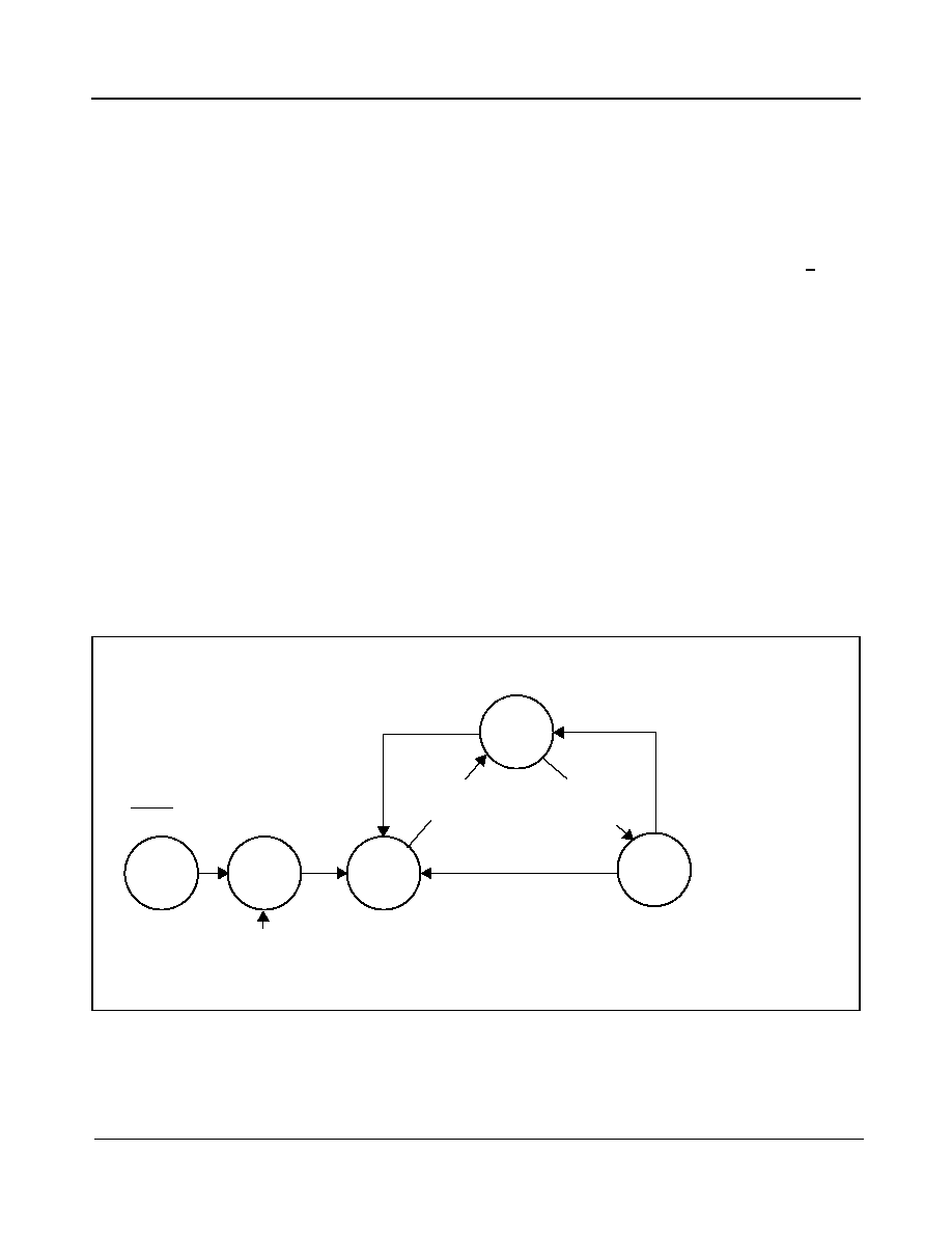
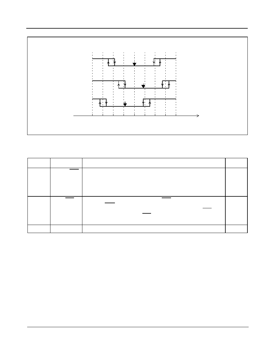
Some of the key elements of the Core PLL are shown in Figure 3 "Core PLL Functional Block Diagram".
Figure 3 - Core PLL Functional Block Diagram
2.2.1 Digitally Controlled Oscillator (DCO)
The DCO is an arithmetic unit that continuously generates a stream of numbers that represent the phase-locked
clock. These numbers are passed to the Clock Synthesizer (see section 2.3) where they are converted into
electrical clock signals of various frequencies
2.2.2 Filters
In Normal mode, the clock generated by the DCO is phase-locked to the input reference signal and band-limited to
meet network synchronization standards. The ZL30407 provides four software programmable (FCS bit in Control
Reg 1 and FCS2 bit in Control Reg 3) and two hardware selectable (FCS pin) filtering options. The filtering
characteristics are similar to a first order low pass filter with corner frequencies that support international standards:
FCS2
(bit)
FCS
(pin/bit)
Filter
Conformance
0
0
1.5 Hz
Meets requirements of G.813 Option 1 and GR-1244 stratum 3 clocks.The
maximum phase slope is limited to 41 ns in 1.326 ms.
0
1
0.1 Hz
Meets requirements of G.813 Option 2, GR-253 for SONET stratum 3 and
GR-253 for SONET Minimum Clocks (SMC).The maximum phase slope is
limited to 885 ns in one second.
1
0
12 Hz
There is no phase slope limiter active in this application.
1
1
6 Hz
Meets requirements of G.813 Option 1 for SDH Equipment Clocks (SEC) and
GR-1244 for Stratum 4 and Stratum 4E clocks. The maximum phase slope is
limited to 50 ns in 1.326 ms.
Table 1 - Loop Filter Selection
FSM
DCO
Filters
Phase
Detector
MUX
LOCK
RefAlign
FCS
HOLDOVER
FCS2
(Control bit only)

ZL30407
Data Sheet
14
Zarlink Semiconductor Inc.
2.2.3 Phase Slope Limiters
Phase slope limiting is achieved by clamping the size of the error term from the phase detector. Limiting the size of
the error term means that the output clocks move slowly in phase as the PLL aligns to phase transients on the input
reference or transients caused by reference rearrangement. This increases the time required to achieve phase
lock, but it is necessary to allow for downstream adjustments and so is called for in network standards such as
G.813, GR-1244 and GR-253. Because the ZL30407 nulls out the phase offset between the output clocks and the
selected reference upon reference rearrangement or return from holdover, the phase slope limiting feature will
generally not come into play. If the pin RefAlign is pulled low to align the equivalent ZL30407 output clock to the
selected reference, a large phase error will have to be corrected. In this case phase slope limiting will be active,
limiting the output phase slope to 0.727 ppm for the 0.1 Hz filter mode, 31 ppm for the 1.5 Hz and the 6 Hz filter
mode. In the 12 Hz mode there is no phase slope limiting. Consequently an output phase slope greater than 31
ppm may occur, for example, in locking to an orthogonal 8 kHz reference.
2.2.4 Lock Indicator (LOCK)
The ZL30407 is considered locked (LOCK = 1) when the residual phase movement after declaring locked condition
does not exceed standard wander generation MTIE and TDEV tests. The ZL30407's phase locking mechanism
allows it to lock within the specified locking times to references with a fractional frequency offset of up to
�
20 ppm.
Locking time for different filters and pulling ranges is listed in "Performance Characteristics*" on page 49.
2.2.5 Reference Alignment (RefAlign)
When the ZL30407 finishes locking to a reference an arbitrary phase difference will remain between its output
clocks and its reference; this phase difference is part of the normal operation of the ZL30407. If so desired, the
output clocks can be brought into phase alignment with the PLL reference (see Figure 21 on page 47) by using the
RefAlign control bit/pin.
2.2.5.1 Using RefAlign with 1.544 MHz, 2.048 MHz or 19.44 MHz Reference
If the ZL30407 is locked to a 1.544 MHz, 2.048 MHz or 19.44 MHz reference, then the output clocks can be brought
into phase alignment with the PLL reference by using the RefAlign control bit/pin according to one of the
procedures below:
1. For 0.1 Hz filtering applications (FCS = 1, FCS2 = 0)
- Wait until the ZL30407 LOCK indicator is high, indicating that it is locked
- Pull FCS low
- Pull Ref/Align low
- Hold RefAlign low for 250
�
s
- Pull RefAlign high
- Wait until the LOCK indicator goes high
- Pull FCS high
After initiating a reference realignment the PLL will enter Holdover mode for 200ns while aligning the internal clocks
to remove the static phase error. The PLL will then begin the normal locking procedure. The LOCK pin will go low 5
sec after the reference realignment is initiated and will remain low for 10 sec.

ZL30407
Data Sheet
15
Zarlink Semiconductor Inc.
2. For 1.5 Hz filtering applications (FCS = 0, FCS2 = 0)
- Wait until the ZL30407 LOCK indication is high, indicating that it is locked
- Pull RefAlign low
- Hold RefAlign low for 250
�
s
- Pull RefAlign high
After initiating a reference realignment the PLL will enter Holdover mode for 200ns while aligning the internal clocks
to remove the static phase error. The PLL will then begin the normal locking procedure. The LOCK pin will go low 5
sec after the reference realignment is initiated and will remain low for 10 sec
3. For 6 Hz and 12 Hz filtering applications (FCS = 1, FCS2 = 1 or FCS = 0, FCS2 = 1 )
- Wait until the ZL30407 LOCK indication is high, indicating that it is locked
- Pull RefAlign low
- Hold RefAlign low for 250
�
s
- Pull RefAlign high
After initiating a reference realignment the PLL will enter Holdover mode for 200 ns while aligning the internal
clocks to remove the static phase error. The PLL will then begin the normal locking procedure. The LOCK pin will
remain high during the realignment process.
2.2.5.2 Using RefAlign with an 8 kHz Reference
If the ZL30407 is locked to an 8 kHz reference, then the output clocks can be brought into phase alignment with the
PLL reference by using the RefAlign control bit/pin according to one of the procedures below:
1. For 0.1 Hz filtering applications (FCS = 1, FCS2 = 0)
- Wait until the ZL30407 LOCK indicator is high, indicating that it is locked
- Pull FCS low
- Pull Ref/Align low
- Hold RefAlign low for 10 sec
- Pull RefAlign high
- Wait until the LOCK indicator goes high
- Pull FCS high
After initiating a reference realignment the PLL will enter Holdover mode for 200ns while aligning the internal clocks
to remove the static phase error. The PLL will then begin the normal locking procedure. The LOCK pin will go low 5
sec after the reference realignment is initiated and will remain low for 10 sec.
2. For 1.5 Hz filtering applications (FCS = 0, FCS2 = 0)
- Wait until the ZL30407 LOCK indication is high, indicating that it is locked
- Pull RefAlign low
- Hold RefAlign low for 10 sec
- Pull RefAlign high
After initiating a reference realignment the PLL will enter Holdover mode for 200ns while aligning the internal clocks
to remove the static phase error. The PLL will then begin the normal locking procedure. The LOCK pin will go low 5
sec after the reference realignment is initiated and will remain low for 10 sec.

ZL30407
Data Sheet
16
Zarlink Semiconductor Inc.
3. For 6 Hz and 12 Hz filtering applications (FCS = 1, FCS2 = 1 or FCS = 0, FCS2 = 1 )
- Wait until the ZL30407 LOCK indication is high, indicating that it is locked
- Pull RefAlign low
- Hold RefAlign low for 3 sec
- Pull RefAlign high
After initiating a reference realignment the PLL will enter Holdover mode for 200ns while aligning the internal clocks
to remove the static phase error. The PLL will then begin the normal locking procedure. The LOCK pin will remain
high during the realignment process.
2.3 Clock Synthesizer
The output of the Core PLL is connected to the Clock Synthesizer that generates twelve clocks and three frame
pulses.
2.3.1 Output Clocks
The ZL30407 provides the following clocks (see Figure 18 "ST-BUS and GCI Output Timing", Figure 19 "DS1 and
DS2 Clock Timing", Figure 20 "C155o and C19o Timing", and Figure 23 "E3 and DS3 Output Timing" for details):
- C1.5o
: 1.544 MHz clock with nominal 50% duty cycle
- C2o
: 2.048 MHz clock with nominal 50% duty cycle
- C4o
: 4.096 MHz clock with nominal 50% duty cycle
- C6o
: 6.312 MHz clock with nominal 50% duty cycle
- C8o
: 8.192 MHz clock with nominal 50% duty cycle
- C8.5o
: 8.592 MHz clock with duty cycle from 30 to 70%.
- C11o
: 11.184 MHz clock with duty cycle from 30 to 70%.
- C16o
: 16.384 MHz clock with nominal 50% duty cycle
- C19o
: 19.44 MHz clock with nominal 50% duty cycle
- C34o
: 34.368 MHz clock with nominal 50% duty cycle
- C44o
: 44.736 MHz clock with nominal 50% duty cycle
- C155
: 155.52 MHz clock with nominal 50% duty cycle.
The ZL30407 provides the following frame pulses (see Figure 18 "ST-BUS and GCI Output Timing" for details). All
frame pulses have the same 125
�
s period (8kHz frequency):
- F0o : 244 ns wide, logic low frame pulse
- F8o : 122 ns wide, logic high frame pulse
- F16o : 61 ns wide, logic low frame pulse
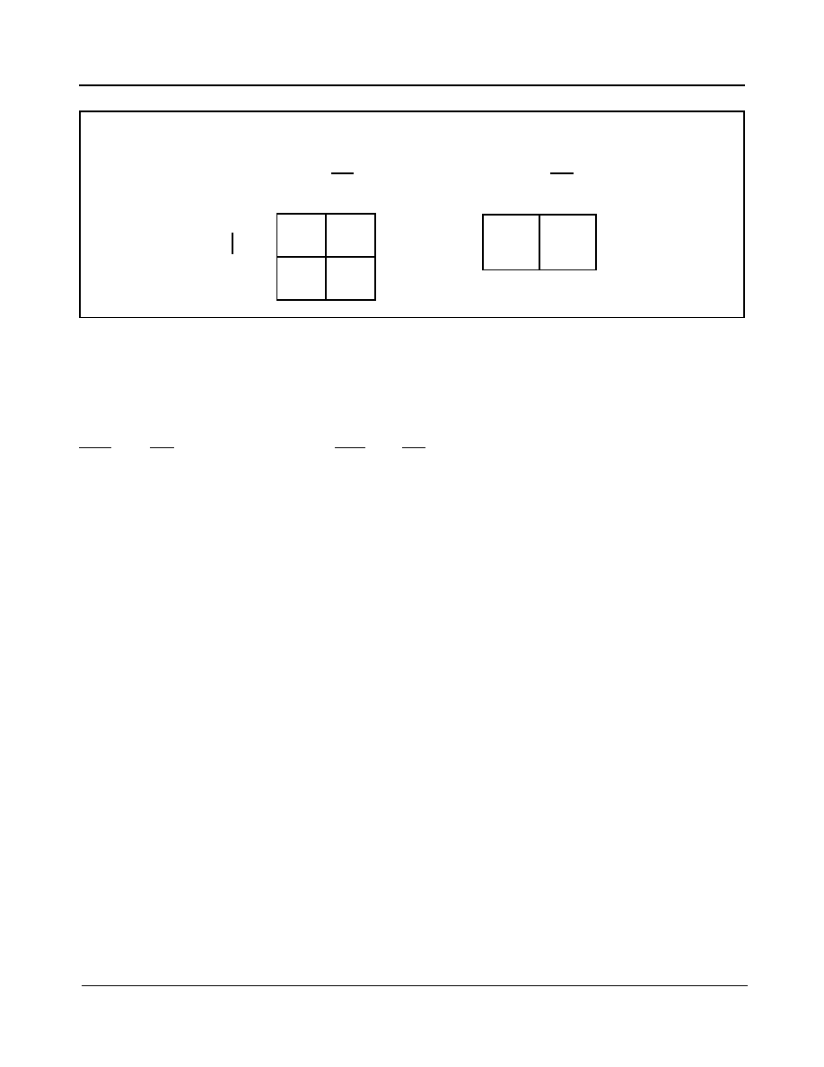
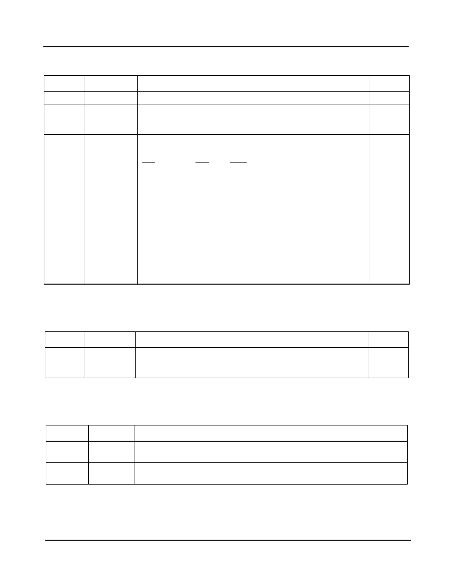
The combination of two pins, E3DS3/OC3 and E3/DS3, controls the selection of different clock configurations.
When the E3DS3/OC3 pin is high then the C155o (155.52 MHz) clock is disabled and the C34/44 clock is output at
its nominal frequency. The logic level on the E3/DS3 input determines if the output clock on the C34/44 output is
34.368 MHz (E3) or 44.736 MHz (DS3) (see Figure 4, "C34/C44, C155o Clock Generation Options," on page 17 for
details).
ZL30407
Data Sheet
17
Zarlink Semiconductor Inc.
Figure 4 - C34/C44, C155o Clock Generation Options
All clocks and frame pulses (except the C155) are output with CMOS logic levels. The C155 clock (155.52 MHz) is
output in a standard LVDS format.
2.3.2 Output Clocks Phase Adjustment
The ZL30407 provides three control registers dedicated to programming the output clock phase offset. Clocks
C16o, C8o, C4o and C2o and frame pulses F16o, F8o, F0o are derived from 16.384 MHz and can be jointly shifted
with respect to an active reference clock by up to 125
�
s with a step size of 61 ns. The required phase shift of
clocks is programmable by writing to the Phase Offset Register 2 ("Table 9") and to the Phase Offset Register 1
("Table 10"). The C1.5o clock can be shifted as well in step sizes of 81 ns by programming C1.5POA bits in Control
Register 3 ("Table 12").
The coarse phase adjustment is augmented with a very fine phase offset control on the order of 477 ps per step.
This fine adjustment is programmable by writing to the Fine Phase Offset Register (Table 16 "Fine Phase Offset
Register (R/W)"). The offset moves all clocks and frame pulses generated by ZL30407 including the C155 clock.
2.4 Control State Machine
2.4.1 Clock Modes
Any Network Element that operates in a synchronous network must support three Clock Modes: Free-run, Normal
(Locked) and Holdover. A network clock will usually operate in Normal mode. The Holdover and Free-run modes
are used to cope with impairments in the synchronization hierarchy. Requirements for Clock Modes are defined in
the international standards e.g.: G.813, GR-1244-CORE and GR-253-CORE and they are enforced by network
operators. The ZL30407 supports all clock modes and each of these modes have a corresponding state in the
Control State Machine.
2.4.2 ZL30407 State Machine
The ZL30407 Control State Machine is a combination of many internal states supporting the three mandatory clock
modes. A simplified version of this state machine is shown in Figure 5; it includes the mandatory states: Free-run,
Normal and Holdover. These three states are complemented by two additional states: Reset and Auto Holdover,
which are critical to the ZL30407 operation under changing external conditions.
C155 Output
C34/44 Output
E3DS3/OC3
E3DS3/OC3
0
0
1
1
155.52
active
disabled
11.184
44.736
8.592
34.368
E3/D
S3
0
1
ZL30407
Data Sheet
18
Zarlink Semiconductor Inc.
Figure 5 - ZL30407 State Machine in Software Control configuration
2.4.2.1 Reset State
The Reset State must be entered when ZL30407 is powered-up. In this state, all arithmetic calculations are halted,
clocks are stopped, the microprocessor port is disabled and all internal registers are reset to their default values.
The Reset state is entered by pulling the RESET pin low for a minimum of
�
1 s. When the RESET pin is pulled back
high, internal logic starts a 625
�
s initialization process before switching into the Free-run state (MS2, MS1 = 10).
2.4.2.2 Free-Run State (Free-Run mode)
The Free-run state is entered when synchronization to the network is not required or is not possible. Typically this
occurs during installation, repairs or when a Network Element operates as a master node in an isolated network. In
the Free-run state, the accuracy of the generated clocks is determined by the accuracy and stability of the ZL30407
Master Crystal Oscillator. When equipment is installed for the first time (or periodically maintained) the accuracy of
the Free-run clocks can be adjusted to within 1x10
-12
by setting the offset frequency in the Master Clock Frequency
Calibration Register.
2.4.2.3 Normal State (Normal Mode or Locked Mode)
The Normal State is entered when a good quality reference clock from the network is available for synchronization.
The ZL30407 automatically detects the frequency of the reference clock (8 kHz, 1.544 MHz, 2.048 MHz or
19.44 MHz) and sets the LOCK status bit and pin high after acquiring synchronization. In the Normal state all
generated clocks (C1.5o, C2o, C4o, C6o, C8o, C16o, C19o, C34/C44 and C155) and frame pulses (F0o, F8o,
F16o) are derived from network timing. To guarantee uninterrupted synchronization, the ZL30407 has two
Acquisition PLLs that continuously monitor the quality of the incoming reference clocks. This dual architecture
enables quick replacement of a poor or failed reference and minimizes the time spent in other states.
Ref: OK AND
MS2,MS1 = 00
{AUTO}
Ref: OK-->FAIL AND
MS2,MS1 = 00
{AUTO}
MS2,MS1 = 01 OR
RefSel change
MS2,MS1 = 10 forces
unconditional return from
any state to Free-run
STATE
MS2,MS1
RESET = 1
Notes:
--> - External transition
{AUTO} - Automatic internal transition
{MANUAL} - User initiated transition
MS2,MS1 = 00
OR
MS2,MS1 = 01
RefSel Change
OR
MS2,MS1 = 01
Ref: FAIL-->OK AND
MS2,MS1 = 00 AND
AHRD = 1 AND MHR = 1
{MANUAL}
Ref: FAIL-->OK AND
MS2,MS1 = 00 AND
AHRD = 0
{AUTO}
OR
AHRD = 1 AND
MHR = 0
RESET
FREE-
RUN
10
HOLD-
OVER
01
NORMAL
00
AUTO
HOLD-
OVER
ZL30407
Data Sheet
19
Zarlink Semiconductor Inc.
2.4.2.4 Holdover State (Holdover Mode)
The Holdover State is typically entered for short durations while network synchronization is temporarily disrupted. In
Holdover Mode, the ZL30407 generates clocks, which are not locked to an external reference signal but their
frequencies are based on stored coefficients in memory that were determined while the PLL was in Normal Mode
and locked to an external reference signal.
The initial frequency offset of the ZL30407 in Holdover Mode is 4x10
-12
(see table Performance Characteristics* on
page 49 for details). This is more accurate than Telcordia's GR-1244-CORE Stratum 3E requirement of +1x10
-9
.
Once the ZL30407 has transitioned into Holdover Mode, holdover stability is determined by the stability of the 20
MHz Master Clock Oscillator. Selection of the oscillator requires close examination of the crystal oscillator
temperature sensitivity and frequency drift caused by aging.
2.4.2.5 Auto Holdover State
The Auto Holdover state is a transitional state that the ZL30407 enters automatically when the active reference fails
unexpectedly. When the ZL30407 detects loss of reference it sets the HOLDOVER status bit and waits in Auto
Holdover state until the failed reference recovers. Recovery from Auto Holdover for 8 kHz, 1.544 MHz, 2.048 MHz
and 19.44 MHz reference clocks is fully automatic, however recovery for an 8 kHz reference clock requires
additional transitioning through the Holdover state to guarantee compliance with network synchronization standards
(for details see Section 4.1.3 on page 36 and Section 4.1.2 on page 35).
The HOLDOVER status may alert the
control processor about the failure and in response the control processor may switch to the secondary reference
clock. The Auto Holdover and Holdover States are internally combined together and they are output as a
HOLDOVER status on pin 55 and bit 4 in Status Register 1 (Table 7 on page 26).
In less demanding clocking arrangements (e.g. Line Cards), the ZL30407 can be configured to operate in the
Hardware Control mode which does not require a microprocessor. Under the Hardware Control mode the ZL30407
maintains most of its State Machine functionality as is shown in Figure 6.
Figure 6 - ZL30407 State Machine in Hardware Control configuration
Ref: OK AND
MS2,MS1 = 00
{AUTO}
Ref: OK-->FAIL AND
MS2,MS1 = 00
{AUTO}
MS2,MS1 = 01 OR
RefSel change
MS2,MS1 = 10 forces
unconditional return from
any state to Free-run
RESET = 1
MS2,MS1 = 00
OR
MS2,MS1 = 01
RefSel Change
OR
MS2,MS1 = 01
Ref: FAIL-->OK AND
MS2,MS1 = 00 AND
{AUTO}
RESET
FREE-
RUN
10
HOLD-
OVER
01
NORMAL
00
AUTO
HOLD-
OVER

ZL30407
Data Sheet
20
Zarlink Semiconductor Inc.
2.4.3 State Transitions
In a typical Network Element application, the ZL30407 will most of the time operate in Normal mode (MS2, MS1 ==
00) generating synchronous clocks. Its two Acquisition PLLs will continuously monitor the input references for signs
of degraded quality and output status information for further processing. The status information from the Acquisition
PLLs and the CORE PLL combined with status information from line interfaces and framers (as listed below) forms
the basis for creating reliable network synchronization.
� Acquisition PLLs (PRIOR, SECOR, PAH, PAFL, SAH, SAFL)
� Core PLL (LOCK, HOLDOVER, FLIM)
� Line interfaces (e.g. LOS - Loss of Signal, AIS - Alarm Indication Signal)
� Framers (e.g. LOF - Loss of frame or Synchronization Status Messages carried over SONET S1 byte or
ESF-DS1 Facility Data Link).
The ZL30407 State Machine is designed to perform some transitions automatically, leaving other less time
dependent tasks to the control processor. The state machine includes two stimulus signals which are critical to
automatic operation: "OK --> FAIL" and "FAIL --> OK" that represent loss (and recovery) of reference signal or its
drift by more than �30000 ppm. Both of them force the Core PLL to transition into and out of the Auto Holdover
state. In case when the reference clock on the PRI (or SEC) input is externally selected from multiple clock sources
with different frequencies then the Acquisition PLL will automatically detect this change as a reference clock failure.
In response, the Acquisition PLL will force Core PLL into Auto-Holdover state until the frequency of a new reference
is determined. This process may take up to 35 ms after which a normal locking procedure will be initiated.
The ZL30407 State Machine is controlled by the mode select pins or bits MS2, MS1. In order to avoid network
synchronization problems, the State Machine has built-in basic protection that does not allow switching the Core
PLL into a state where it cannot operate correctly e.g., it is not possible to force the Core PLL into Normal mode
when all references are lost.
2.5 Master Clock Frequency Calibration Circuit
In an ordinary timing generation module, the Free-run mode accuracy of generated clocks is determined by the
accuracy of the Master Crystal Oscillator. If the Master Crystal Oscillator has a manufacturing tolerance of
�
4.6 ppm, the generated clocks will have no better accuracy.
The ZL30407 eliminates Crystal Oscillator tolerance problem by providing a programmable Master Clock
Frequency Calibration circuit, which can reduce oscillator manufacturing tolerance to near zero. However this
feature does not eliminate oscillator frequency drift. The value stored in the Master Clock Calibration Register can
be periodically updated to compensate for oscillator frequency drift due to ageing or due to temperature effects. The
compensation value for the Master Clock Calibration Register (MCFC3 to MCFC0) can be calculated from the
following equation:
MCFC = 45036 * (-f
offset
) where: f
offset
= f
m
- 20 000 000 Hz
The f
m
frequency should only be measured after the Master Crystal Oscillator has been mounted inside a system
and powered long enough for the Master Crystal Oscillator to reach a steady operating temperature. Section 4.3 on
page 40 provides two examples of how to calculate an offset frequency and convert the decimal value to a binary
format. The maximum frequency compensation range of the MCFC register is equal to
�
2384 ppm (
�
47680 Hz).
Changes to the Master Clock Calibration Register cause immediate changes in the frequency of the output clocks.
Care should be taken to ensure that changes to the Master Clock Calibration Register are made in small
increments so the frequency steps can be tolerated by downstream equipment. A rate of frequency change below
2.9 ppm/sec is suggested.
All memory in the ZL30407 is volatile; so any settings of the Master Clock Calibration Register need to be reloaded
after each RESET.

ZL30407
Data Sheet
21
Zarlink Semiconductor Inc.
2.6 Microprocessor Interface
The ZL30407 can be controlled by a microprocessor or by an ASIC type of device that is connected directly to the
hardware control pins. If the HW pin is tied low (see Figure 7 "Hardware and Software Control Options"), an 8-bit
Motorola type microprocessor may be used to control PLL operation and check its status. Under software control,
the control pins MS2, MS1, FCS, RefSel, RefAlign are disabled and they are replaced by the equivalent control bits.
The output pins LOCK, HOLDOVER, PRIOR and SECOR are always active and they provide current status
information whether the device is in microprocessor or hardware control. Software (microprocessor) control
provides additional functionality that is not available in hardware control such as:
� 6 Hz and 12 Hz PLL loop filter selection
� output clock phase adjustment
� master clock frequency calibration
� extended access to status registers.These registers are also accessible when the ZL30407 operates under
Hardware control.
2.7 JTAG Interface
The ZL30407 JTAG (Joint Test Action Group) interface conforms to the Boundary-Scan standard IEEE1149.1-1990,
which specifies a design-for-testability technique called Boundary-Scan Test (BST). The BST architecture is made
up of four basic elements, Test Access Port (TAP), TAP Controller, Instruction Register (IR) and Test Data Registers
(TDR) and all these elements are implemented on the ZL30407.
Zarlink Semiconductor provides a Boundary Scan Description Language (BSDL) file that contains all the
information required for a JTAG test system to access the ZL30407's boundary scan circuitry. The file is available
for download from the Zarlink Semiconductor web site: www.zarlink.com.
3.0 Hardware and Software Control
The ZL30407 offers Hardware and Software Control options that simplify the design of basic or complex clock
synchronization modules. Hardware control offers fewer features but still allows for building of sophisticated timing
cards without extensive programming. The complete set of control and status functions for each mode are shown in
Figure 7 "Hardware and Software Control Options".

ZL30407
Data Sheet
22
Zarlink Semiconductor Inc.
Figure 7 - Hardware and Software Control Options
3.1 Hardware Control
The Hardware control is a subset of software control and it will only be briefly described with cross-referencing to
Software control programmable registers.
3.1.1 Control Pins
The ZL30407 has five dedicated control pins for selecting modes of operation and activating different functions.
These pins are listed below:
MS2 and MS1 pins: Mode Select: The MS2 (pin 19) and MS1 (pin 18) inputs select the PLL mode of operation.
See Table 2 for details. The logic level at these inputs is sampled by the rising edge of the F8o frame pulse.
MS2
MS1
Mode of Operation
0
0
Normal mode
0
1
Holdover mode
1
0
Free-run
1
1
Reserved
Table 2 - Operating Modes and States
Hardware Control
Software Control
HW = 1
C
O
N
T
R
O
L
S
T
A
T
U
S
C
O
N
T
R
O
L
S
T
A
T
U
S
MS2
MS1
FCS
FCS2
RefSel
RefAlign
AHRD
MHR
HW = 0
LOCK
HOLDOVER
PRIOR
SECOR
FLIM
PAH
PAFL
SAH
SAFL
Pins
LOCK
HOLDOVER
PRIOR
SECOR
MS2
MS1
FCS
RefSel
RefAlign
Processor
Interface
ZL30407
Data Sheet
23
Zarlink Semiconductor Inc.
FCS pin: Filter Characteristic Select. The FCS (pin 9) input is used to select the filtering characteristics of the
Core PLL. See Table 1, "Loop Filter Selection" on page 13 for details.
RefSel: Reference Source Select. The RefSel (pin 47) input selects the PRI (primary) or SEC (secondary) input
as the reference clock for the Core PLL. The logic level at this input is sampled by the rising edge of F8o.
RefAlign: Reference Alignment. The RefAlign (pin 48) input controls phase realignment between the input
reference and the generated output clocks.
3.1.2 Status Pins
The ZL30407 has four dedicated status pins for indicating modes of operation and quality of the Primary and
Secondary reference clocks. These pins are listed below:
LOCK - This output goes high after the ZL30407 has completed its locking sequence (see section 2.2.3 for details).
HOLDOVER - This output goes high when the Core PLL enters Holdover mode. The Core PLL will switch to
Holdover mode if the respective Acquisition PLL enters Holdover mode or if the mode select pins or bits are set to
Holdover (MS2, MS1 = 01).
PRIOR - This output goes high when the primary reference frequency deviates from the PLL center frequency by
more than �12 ppm. See PRIOR pin description for details.
SECOR - This output goes high when the secondary reference frequency deviates from the PLL center frequency
by more than �12 ppm. See SECOR pin description for details.
3.2 Software Control
Software control is enabled by setting the HW pin to logic zero (HW = 0). In this mode all hardware control pins
(inputs) are disabled and all status pins remain enabled. The ZL30407 has a number of registers that provide all the
functionality available in Hardware control and in addition they offer advanced control and monitoring that is only
available in Software control (see Figure 7 "Hardware and Software Control Options").
3.2.1 Control Bits
The ZL30407 has a number of registers that provide greater operational flexibility than available pins in Hardware
control (see Figure 7 "Hardware and Software Control Options"). The MS2, MS1, FCS2,
FCS, RefSel and RefAlign
bits perform the same function as the corresponding pins. Two additional bits AHRD and MHR support recovery
from Auto Holdover mode and they are described in section 3.2.4.
FCS
Filtering Characteristic
0
Filter corner frequency set to 1.5 Hz
1
Filter corner frequency set to 0.1 Hz
Table 3 - Filter Characteristic Selection
RefSel
Input Reference
0
Core PLL connected to the Primary Acquisition PLL
1
Core PLL connected to the Secondary Acquisition PLL
Table 4 - Reference Source Select
ZL30407
Data Sheet
24
Zarlink Semiconductor Inc.
In addition to the Control bits shown in Figure 7 "Hardware and Software Control Options", the ZL30407 has a
number of bits and registers that are accessed infrequently e.g., 6 Hz and 12 Hz PLL loop filter selection, Phase
Offset Adjustment or Master Clock Frequency Calibration. These additional control options add flexibility to the
ZL30407.
The ZL30407 has a number of status bits that provide more comprehensive monitoring of the internal operation
than is available in Hardware control (see Figure 7 "Hardware and Software Control Options"). The HOLDOVER,
PRIOR and SECOR bits perform the same function as their equivalent status pins. The function of the LOCK status
bit is not identical to the function of the LOCK status pin, see the description of the LOCK status bit and the FLIM
status bit for details. The FLIM bit indicates that the output frequency of the Core PLL has reached its upper or
lower limit. The PAH and SAH status bit show entry of the Primary and Secondary acquisition PLLs into Holdover
mode. See section 3.2.4 for detailed description of the status bits. Under software control, the status pins are
always enabled and they can be used to trigger hardware interrupts.
3.2.2 ZL30407 Register Map
Addresses: 00H to 6FH
Note: The ZL30407 uses address space from 00h to 6Fh. Registers at address locations not listed above must not be written or read.
Address
hex
Register
Read
Write
Function
00
Control Register 1
R/W
RefSel, 0, 0, MS2, MS1, FCS, 0, RefAlign
01
Status Register 1
R
PRIOR, SECOR, LOCK, HOLDOVER, rsv, FLIM, rsv, rsv
04
Control Register 2
R/W
E3DS3/OC3, E3/DS3, 0, 0, 0, 0, 0, 0,
06
Phase Offset Register 2
R/W
0, 0, 0, 0, OffEn, C16POA10, C16POA9, C16POA8
07
Phase Offset Register 1
R/W
C16POA7, C16POA6, C16POA5, C16POA4, C16POA3,
C16POA2, C16POA1, C16POA0
0F
Device ID Register
R
0111 0000
11
Control Register 3
R/W
rsv, rsv, C1.5POA2, C1.5POA1, C1.5POA0, 0, 0, FCS2
13
Clock Disable Register 1
R/W
0, 0, C16dis, C8dis, C4dis, C2dis, C1.5dis,0
14
Clock Disable Register 2
R/W
0, 0, 0, F8odis, F0odis, F16odis, C6dis, C19dis
19
Core PLL Control Register
R/W
0, 0, 0, 0, 0, MHR, AHRD, 0
1A
Fine Phase Offset Register
R/W
FPOA7, FPOA6, FPOA5, FPOA4, FPOA3, FPOA2,
FPOA1, FPOA0
20
Primary Acquisition PLL
Status Register
R
rsv, rsv, rsv, InpFreq1, InpFreq0, rsv, PAH,PAFL
28
Secondary Acquisition PLL
Status Register
R
rsv, rsv, rsv, InpFreq1, InpFreq0, rsv, SAH, SAFL
40
Master Clock Frequency
Calibration Register - Byte 4
R/W
MCFC31, MCFC30, MCFC29, MCFC28, MCFC27,
MCFC26, MCFC25, MCFC24,
41
Master Clock Frequency
Calibration Register - Byte 3
R/W
MCFC23, MCFC22, MCFC21, MCFC20, MCFC19,
MCFC18, MCFC17, MCFC16
42
Master Clock Frequency
Calibration Register - Byte 2
R/W
MCFC15, MCFC14, MCFC13, MCFC12, MCFC11,
MCFC10, MCFC9, MCFC8
43
Master Clock Frequency
Calibration Register - Byte 1
R/W
MCFC7, MCFC6, MCFC5, MCFC4, MCFC3, MCFC2,
MCFC1, MCFC0
Table 5 - ZL30407 Register Map
ZL30407
Data Sheet
25
Zarlink Semiconductor Inc.
3.2.3 Register Description
Address: 00 H
Bit
Name
Functional Description
Default
7
RefSel
Reference Select. A zero selects the PRI (Primary) reference source
as the input reference signal and a one selects the SEC (secondary)
reference.
0
6-5
RSV
Reserved
00
4-3
MS2, MS1
Mode Select
- MS2 = 0 MS1 = 0 Normal Mode (Locked Mode)
- MS2 = 0 MS1 = 1 Holdover Mode
- MS2 = 1 MS1 = 0 Free-run Mode
- MS2 = 1 MS1 = 1 Reserved
10
2
FCS
Filter Characteristic Select (see Table 12 on page 29 for
complimentary FCS2 bit description)
- FCS2 = 0, FCS = 0 : Filter corner frequency set to 1.5 Hz.
- FCS2 = 0, FCS = 1 : Filter corner frequency set to 0.1 Hz.
- FCS2 = 1, FCS = 0 : Filter corner frequency set to 12 Hz.
- FCS2 = 1, FCS = 1 : Filter corner frequency set to 6 Hz.
Conformance of these filter settings to standards is presented in
Table 1, "Loop Filter Selection" on page 13.
0
1
RSV
Reserved
0
0
RefAlign
Reference Alignment. A high-to-low transition aligns the generated
output clocks to the input reference signal (see Section 2.2.5,
Reference Alignment (RefAlign) for details). This bit should never be
held low permanently.
1
Table 6 - Control Register 1 (R/W)
ZL30407
Data Sheet
26
Zarlink Semiconductor Inc.
Address: 01 H
Bit
Name
Functional Description
7
PRIOR
Primary Reference Out of Range. This output goes high when:
� the primary reference is off its nominal frequency by more than
�
12 ppm. The
frequency offset monitor updates internally every 10 sec and will change state
after two matching measurements (PASS/PASS or FAIL/FAIL). This is in full
compliance with the GR-1244-CORE requirement of 10 to 30 sec Reference
Validation Time. This output returns to zero when the reference frequency is
requalified within
�
9.2 ppm of the nominal frequency (monitor circuit has built-in
hysteresis). In an extreme case, when over time the Master Clock oscillator
drifts
�
4.6 ppm the switching thresholds will change as well, as is shown in
Figure 8.
� the reference impairment detector detects large frequency offset (greater than
3%) or large change in a single cycle period (greater than 30%). In both cases
detector will disqualify the reference and reset the 10 sec internal timer.
6
SECOR
Secondary Reference Out of Range. Functionally, this bit is equivalent to the
PRIOR bit for Primary Acquisition PLL.
5
LOCK
Lock. This bit goes high when the Core PLL completes the phase locking process to
the input reference clock (see Section 2.2.4, Lock Indicator (LOCK) for details). After
achieving lock, this bit will go low if the ZL30407 enters Holdover mode, Automatic
Holdover mode or Free-run mode, or if the Core PLL phase detector accumulates
more than 22
�
s of phase error, or if the RefAlign control bit/pin is taken low.
Note that the indication of the LOCK status pin is a logical combination of the LOCK
status bit and the FLIM status bit. Please see the FLIM status bit description.
4
HOLDOVER
Holdover. This bit goes high when the Core PLL enters Holdover mode. Detection of
reference failure and subsequent transition from Normal to Holdover mode takes
approximately: 0.75
�
s for 19.44 MHz reference, 0.85
�
s for 2.048 MHz reference,
1.5
�
s for 1.544 MHz reference and 130
�
s for 8 kHz reference.
3
RSV
Reserved
2
FLIM
Frequency Limit. This bit goes high when the Core PLL is pulled by the input
reference signal to the edge of its frequency tracking range set at
�
104 ppm. This bit
may change state momentarily in the event of large jitter or wander excursions
occurring when the input reference is close to the frequency limit range.
When the FLIM bit goes high it will cause the LOCK status pin to go low, but it will not
cause the LOCK status bit to go low.
1
RSV
Reserved
0
RSV
Reserved
Table 7 - Status Register 1 (R)
ZL30407
Data Sheet
27
Zarlink Semiconductor Inc.
Figure 8 - Primary and Secondary Reference Out of Range Thresholds
Address: 04 H
Bit
Name
Functional Description
Default
7
E3DS3/OC3
E3, DS3 or OC-3 clock select. Setting this bit to zero enables the
C155P/N outputs (pin 30 and pin 31) and enables the C34/C44 output
(pin 53) to provide C8 or C11 clocks. Logic high disables the C155
clock LVDS outputs and enables the C34/C44 output to provide a C34
or C44 clock.
0
6
E3/DS3
E3 or DS3 clock select. When E3DS3/OC3 bit is set high, a logic low
on the E3/DS3 bit selects a 44.736 MHz clock on the C34/C44 output
and logic high selects a 34.368 MHz clock. When the E3DS3/OC3 bit is
set low, a logic low on the E3/DS3 bit selects an 11.184 MHz clock on
the C34/C44 output and a logic high selects an 8.592 MHz clock.
0
5-0
RSV
Reserved
000000
Table 8 - Control Register 2 (R/W)
C20i Clock
0 ppm
+4.6 ppm
-4.6 ppm
Accuracy
-9.2
0
7.4
12
-12
9.2
C20
C20
-7.4 -4.6
4.6
13.8 16.6
4.6
-4.6
-16.6 -13.8
-15
-10
0
-20
-5
5
10
15
20
Frequency
Out of Range
Out of Range
Out of Range
In Range
In Range
In Range
Offset [ppm]
0
0
C20
ZL30407
Data Sheet
28
Zarlink Semiconductor Inc.
Address: 06 H
Address: 07 H
Address: 0F H
Bit
Name
Functional Description
Default
7-4
RSV
Reserved
0000
3
OffEn
Offset Enable. Set high to enable programmable phase offset
adjustment (C16 Phase Offset Adjustment and C1.5 Phase Offset
Adjustment) between the input reference and the generated clocks.
0
2 - 0
C16POA10
to
C16POA8
C16 Phase Offset Adjustment. These three bits (most significant) in
conjunction with the eight bits of Phase Offset Register 1 allow for
phase shifting of all clocks and frame pulses that are derived from the
C16 clock (C8o, C4o, C2o, F16o, F8o, F0o). The phase offset is an
unsigned number in a range from 0 to 2047. Each increment by one
represents a phase-offset advancement by 61.035 ns with respect to
the input reference signal. The phase offset is a two-byte value and it
must be written in one step increments. For example: four writes are
required to advance clocks by 244 ns from its current position of 22H:
write 23H, 24H, 25H, 26H. Writing numbers in reverse order will delay
clocks from their present position.
Note that phase offset adjustment is a process of shifting clocks in a
time domain which may cause momentary distortion of the generated
clocks. Therefore it is not recommended to perform phase offset
adjustments on an active ZL30407 (at the time when it generates
network clocks).
000
Table 9 - Phase Offset Register 2 (R/W)
Bit
Name
Functional Description
Default
7-0
C16POA7
to
C16POA0
C16 Phase Offset Adjustment. The eight least significant bits of the
phase offset adjustment word. See the Phase Offset Register 2 for
details.
0000
0000
Table 10 - Phase Offset Register 1 (R/W)
Bit
Name
Functional Description
7-4
ID7 - 4
Device Identification Number. These four bits represent the device part number.
The ID number for ZL30407 is 0111.
3-0
ID3 - 0
Device Revision Number. These bits represent the revision number. Number
starts from 0000.
Table 11 - Device ID Register (R)
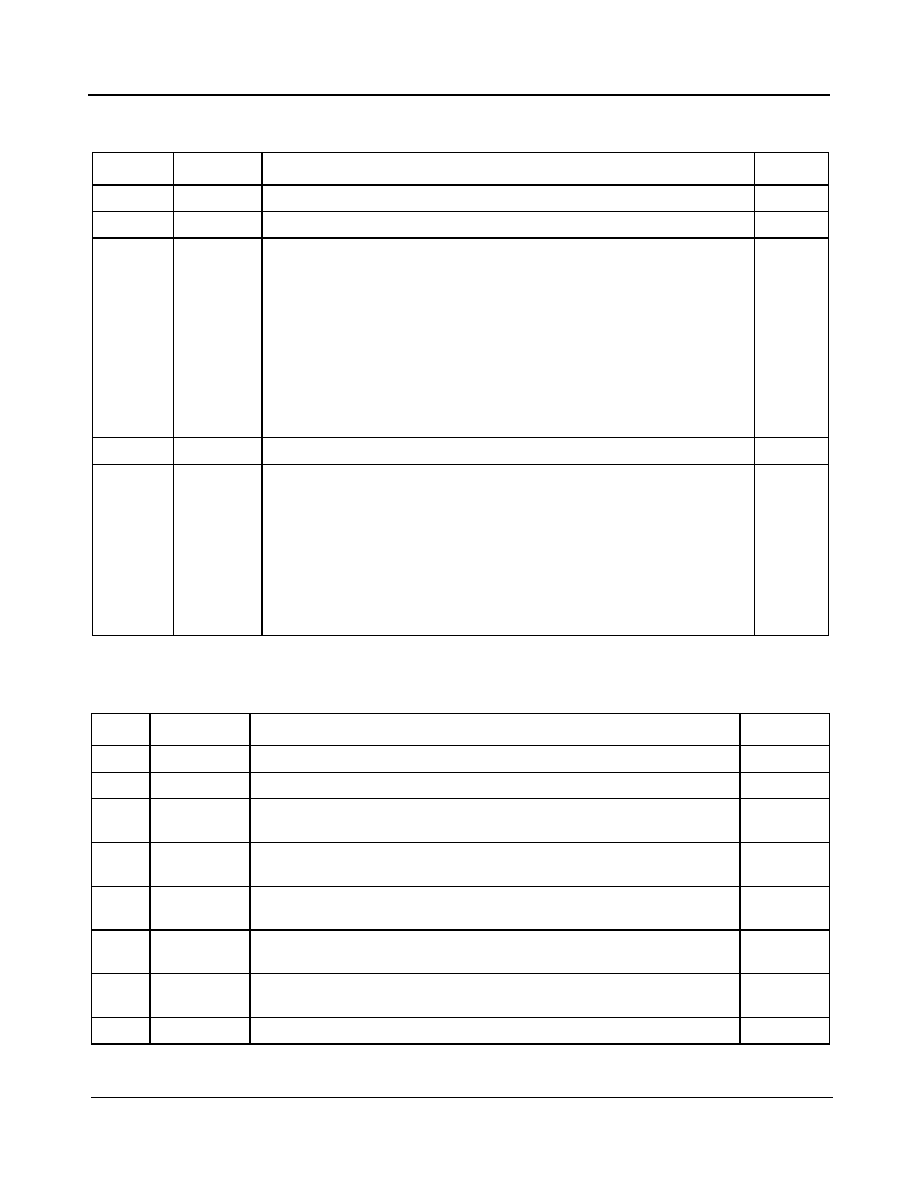
ZL30407
Data Sheet
29
Zarlink Semiconductor Inc.
Address: 11 H
Address: 13 H
Bit
Name
Functional Description
Default
7
RSV
Reserved
0
6
RSV
Reserved
0
5-3
C1.5POA2
to
C1.5POA0
C1.5 Phase Offset Adjustment. These three bits allow for changing of
the phase offset of the C1.5o clock relative to the active input reference.
The phase offset is an unsigned number in a range from 0 to 7. Each
increment by one represents phase-offset advancement by 80.96 ns.
Example: Writing 010 advances C1.5 clock by 162 ns. Successive writing
of 001 delays this clock by 80.96 ns from its present position
Note that phase offset adjustment is a process of shifting clocks in a time
domain which may cause momentary distortion of the generated clocks.
Therefore it is not recommended to perform phase offset adjustments on
an active ZL30407 (at the time when it generates network clocks).
000
2-1
RSV
Reserved
00
0
FCS2
Filter Characteristic Select 2 (see Table 6 on page 25 for
complimentary FCS bit description)
- FCS2 = 0, FCS = 0 : Filter corner frequency set to 1.5 Hz
- FCS2 = 0, FCS = 1 : Filter corner frequency set to 0.1 Hz
- FCS2 = 1, FCS = 0 : Filter corner frequency set to 12 Hz
- FCS2 = 1, FCS = 1 : Filter corner frequency set to 6 Hz
Conformance of these filter settings to standards is presented in Table 1,
"Loop Filter Selection" on page 13.
0
Table 12 - Control Register 3 (R/W)
Bit
Name
Functional Description
Default
7
RSV
Reserved
0
6
RSV
Reserved
0
5
C16dis
16.384 MHz Clock Disable. When set high, this bit tristates the
16.384 MHz clock output.
0
4
C8dis
8.192 MHz Clock Disable. When set high, this bit tristates the
8.192 MHz clock output.
0
3
C4dis
4.096 MHz Clock Disable. When set high, this bit tristates the
4.096 MHz clock output.
0
2
C2dis
2.048 MHz Clock Disable. When set high, this bit tristates the
2.048 MHz clock output.
0
1
C1.5dis
1.544 MHz Clock Disable. When set high, this bit tristates the
1.544 MHz clock output.
0
0
RSV
Reserved
0
Table 13 - Clock Disable Register 1 (R/W)
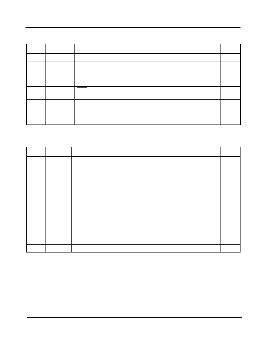
ZL30407
Data Sheet
30
Zarlink Semiconductor Inc.
Address: 14 H
Address: 19 H
Bit
Name
Functional Description
Default
7-5
RSV
Reserved
000
4
F8odis
F8o Frame Pulse Disable. When set high, this bit tristates the 8 kHz
122 ns active high framing pulse output.
0
3
F0odis
F0o Frame Pulse Disable. When set high, this bit tristates the 8 kHz
244 ns active low framing pulse output.
0
2
F16odis
F16o Frame Pulse Disable. When set high, this bit tristates the 8 kHz
61 ns active low framing pulse output.
0
1
C6dis
6.312 MHz Clock Disable. When set high, this bit tristates the 6.312 MHz
clock output.
0
0
C19dis
19.44 MHz Clock Disable. When set high, this bit tristates the 19.44 MHz
clock output.
0
Table 14 - Clock Disable Register 2 (R/W)
Bit
Name
Functional Description
Default
7-3
RSV
Reserved
00000
2
MHR
Manual Holdover Release. A change form 0 to 1 on the MHR bit will release
the Core PLL from Auto Holdover when automatic return from Holdover is
disabled (AHRD is set to 1). This bit is level sensitive and it must be cleared
immediately after it is set to 1 (next write operation). This bit has no effect if
AHRD is set to 0.
0
1
AHRD
Automatic Holdover Return Disable. When set high, this bit inhibits the
Core PLL from automatically switching back to Normal mode from Auto
Holdover state when the active Acquisition PLL regains lock to its input
reference. The active Acquisition PLL is the Acquisition PLL to which the
Core PLL is currently connected.
For the 8 kHz input reference, the recovery from Auto Holdover state must
transition through the Holdover state to preserve "hit-less" recovery. To
guarantee this transitioning, the AHDR bit should be set high permanently to
prevent automatic return to Normal mode.
0
0
RSV
Reserved
0
Table 15 - Core PLL Control Register (R/W)
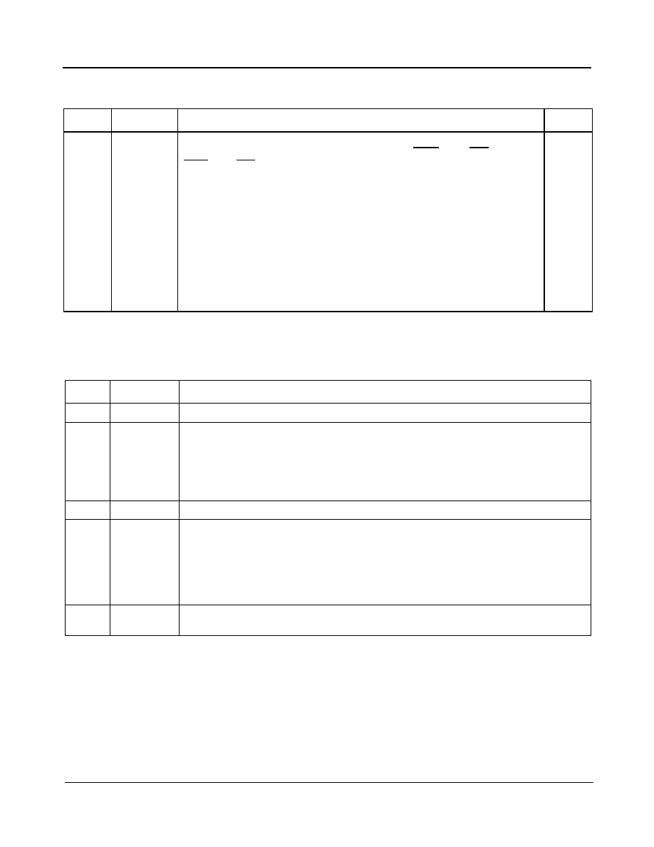
ZL30407
Data Sheet
31
Zarlink Semiconductor Inc.
Address: 1A H
Address: 20 H
Bit
Name
Functional Description
Default
7-0
FPOA7 - 0
Fine Phase Offset Adjustment. This register allows phase offset
adjustment of all output clocks and frame pulses (C16o, C8o, C4o, C2o,
F16o, F8o, F0o, C155, C19o, C34/44, C1.5o, C6o) relative to the active input
reference. The adjustment can be positive (advance) or negative (delay) with
a nominal step size of 477 ps (61.035 ns / 128). Changes to the offset values
are filtered before they propagate to the PLL outputs. The rate of phase
change is determined by the bandwidth of the selected filter and is limited to
the level listed in the Table , "Performance Characteristics*" on page 49.
The phase offset value is a signed 2's complement number e.g.:
Advance: +1 step = 01H, +2 steps = 02H, +127 steps = EFH
Delay: -1 step = FFH, -2 steps = FEH, -128 steps = 80H
Example: Writing 08H advances all clocks by 3.8 ns and writing F3H delays
all clocks
00000
000
Table 16 - Fine Phase Offset Register (R/W)
Bit
Name
Functional Description
7-5
RSV
Reserved
4-3
InpFreq1-0
Input Frequency. These two bits identify the Primary Reference Clock frequency.
- 00 = 19.44 MHz
- 01 = 8 kHz
- 10 = 1.544 MHz
- 11 = 2.048 MHz
2
RSV
Reserved
1
PAH
Primary Acquisition PLL Holdover. This bit goes high whenever the Acquisition PLL
enters Holdover mode. Holdover mode is entered when the reference frequency is:
� lost completely
� drifts more than
�
30 000 ppm off from the nominal frequency
� a large phase hit occurs on the reference clock
0
PAFL
This status bit is intended to provide software compatibility with the ZL30402. It is not
required for new designs.
Table 17 - Primary Acquisition PLL Status Register (R)
ZL30407
Data Sheet
32
Zarlink Semiconductor Inc.
Address: 28 H
Address: 40 H
Address: 41 H
Address: 42 H
Bit
Name
Functional Description
7-5
RSV
Reserved
4-3
InpFreq1-0
Input Frequency. These two bits identify the Secondary Reference Clock frequency.
- 00 = 19.44 MHz
- 01 = 8 kHz
- 10 = 1.544 MHz
- 11 = 2.048 MHz
2
RSV
Reserved
1
SAH
Secondary Acquisition PLL Holdover. This bit goes high whenever the Acquisition
PLL enters Holdover mode. Holdover mode is entered when reference frequency is:
� lost completely
� drifts more than
�
30 000 ppm off the nominal frequency
� a large phase hit occurs on the reference clock
0
SAFL
This status bit is intended to provide software compatibility with the ZL30402. It is not
required for new designs.
Table 18 - Secondary Acquisition PLL Status Register (R)
Bit
Name
Functional Description
Default
7-0
MCFC31 - 24
Master Clock Frequency Calibration. This most significant byte
contains the 31st to 24th bit of the Master Clock Frequency
Calibration Register. See Applications section 4.2 for a detailed
description of how to calculate the MCFC value.
00000
000
Table 19 - Master Clock Frequency Calibration Register 4 (R/W)
Bit
Name
Functional Description
Default
7-0
MCFC23 - 16
Master Clock Frequency Calibration. This byte contains the 23rd
to 16th bit of the Master Clock Frequency Calibration Register.
00000
000
Table 20 - Master Clock Frequency Calibration Register 3 (R/W)
Bit
Name
Functional Description
Default
7-0
MCFC15 - 8
Master Clock Frequency Calibration. This byte contains the 15th
to 8th bit of the Master Clock Frequency Calibration Register.
00000
000
Table 21 - Master Clock Frequency Calibration Register 2 (R/W)

ZL30407
Data Sheet
33
Zarlink Semiconductor Inc.
Address: 43 H
4.0 Applications
This section contains application specific details for Mode Switching and Master Clock Oscillator calibration.
4.1 ZL30407 Mode Switching - Examples
The ZL30407 is designed to transition from one mode to the other driven by the internal State Machine or by
manual control. The following examples present a couple of typical scenarios of how the ZL30407 can be employed
in network synchronization equipment (e.g. timing modules, line cards or stand alone synchronizers).
Bit
Name
Functional Description
Default
7-0
MCFC7 - 0
Master Clock Frequency Calibration. This byte contains bit 7 to
bit 0 of the Master Clock Frequency Calibration Register.
00000
000
Table 22 - Master Clock Frequency Calibration Register 1 (R/W)
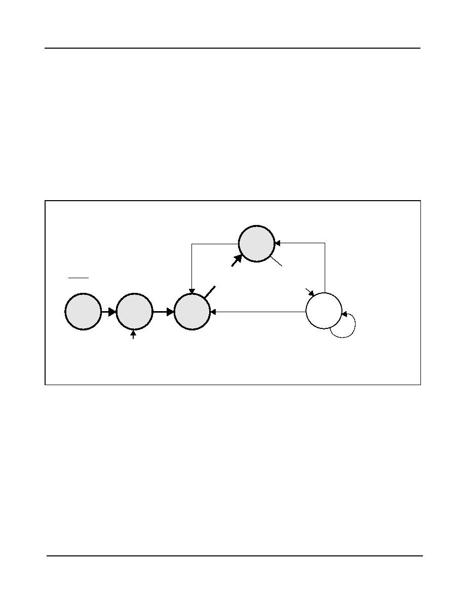
ZL30407
Data Sheet
34
Zarlink Semiconductor Inc.
4.1.1 System Start-up Sequence: FREE-RUN --> HOLDOVER --> NORMAL
The FREE-RUN to HOLDOVER to NORMAL transition represents a sequence of steps that will most likely occur
during a new system installation or scheduled maintenance of timing cards. The process starts from the RESET
state and then transitions to Free-run mode where the system (card) is being initialized. At the end of this process
the ZL30407 should be switched into Normal mode (with MS2, MS1 set to 00) instead of Holdover mode. If the
reference clock is available, the ZL30407 will transition briefly into Holdover to acquire synchronization and switch
automatically to Normal mode. If the reference clock is not available at this time, as it may happen during new
system installation, then the ZL30407 will stay in Holdover indefinitely. While in Holdover mode, the Core PLL will
continue generating clocks with the same accuracy as in the Free-run mode, waiting for a good reference clock.
When the system is connected to the network (or timing card switched to a valid reference) the Acquisition PLL will
quickly synchronize and clear its own Holdover status (PAH bit). This will enable the Core PLL to start the
synchronization process. After acquiring lock, the ZL30407 will automatically switch from Holdover into Normal
mode without system intervention. This transition to the Normal mode will be flagged by the LOCK status bit and
pin.
Figure 9 - Transition From Free-run to Normal Mode
Ref: OK AND
MS2,MS1 = 00
{AUTO}
Ref: OK-->FAIL AND
MS2,MS1 = 00
{AUTO}
MS2,MS1 = 01 OR
RefSel change
MS2,MS1 = 10 forces
unconditional return from
any state to Free-run
RESET = 1
MS2,MS1 = 00
OR
MS2,MS1 = 01
RefSel Change
OR
MS2,MS1 = 01
Ref: FAIL-->OK AND
MS2,MS1 = 00 AND
AHRD = 1 AND MHR = 1
{MANUAL}
Ref: FAIL-->OK AND
MS2,MS1 = 00 AND
AHRD = 0
{AUTO}
OR
AHRD = 1 AND
MHR = 0
RESET
FREE-
RUN
10
HOLD-
OVER
01
NORMAL
00
AUTO
HOLD-
OVER
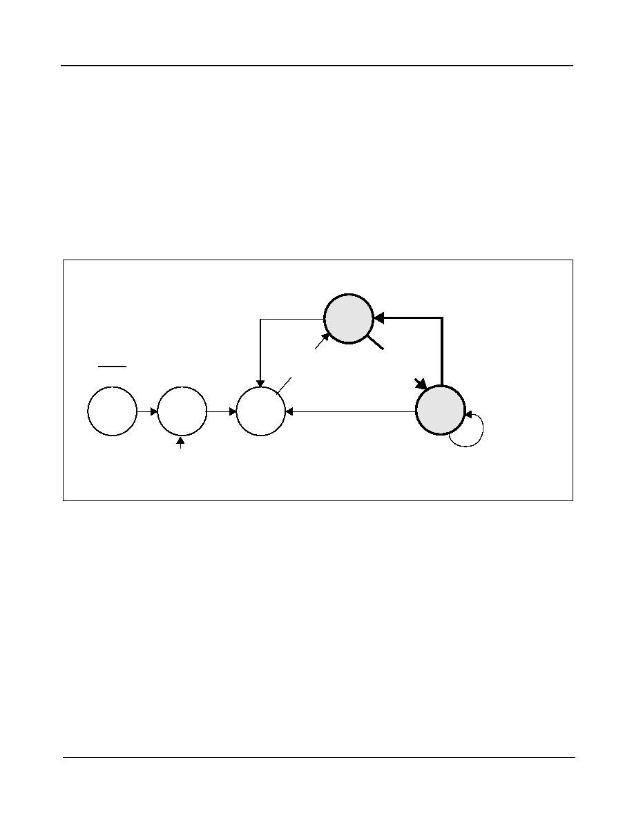
ZL30407
Data Sheet
35
Zarlink Semiconductor Inc.
4.1.2 Single Reference Operation: NORMAL --> AUTO HOLDOVER --> NORMAL
The NORMAL to AUTO-HOLDOVER to NORMAL transition will usually happen when the Network Element loses
its single reference clock unexpectedly. The sequence starts with the reference clock transitioning from OK --> FAIL
at a time when ZL30407 operates in Normal mode (as is shown in Figure 10). This failure is detected by the active
Acquisition PLL based on the following FAIL criteria:
� Frequency offset on 8 kHz, 1.544 MHz, 2.048 MHz and 19.44 MHz reference clocks exceeds �30000 ppm
(�3%).
� Single phase hit on 1.544 MHz, 2.048 MHz and 19.44 MHz exceeds half of the cycle of the reference clock
After detecting any of these anomalies on a reference clock the Acquisition PLL will switch itself into Holdover mode
forcing the Core PLL to automatically switch into the Auto Holdover state. This condition is flagged by LOCK = 0
and HOLDOVER = 1.
Figure 10 - Automatic Entry into Auto Holdover State and Recovery into Normal Mode
There are two possible returns to Normal mode after the reference signal is restored:
� With the AHRD (Automatic Holdover Return Disable) bit set to 0. In this case the Core PLL will automatically
return to the Normal state after the reference signal recovers from failure. This transition is shown on the
state diagram as a FAIL --> OK change. This change becomes effective when the reference is restored and
there have been no phase hits detected for at least 64 clock cycles for the 1.544/2.048 MHz reference, 512
clock cycles for the 19.44 MHz reference and 1 clock cycle for the 8 kHz reference.
� With the AHRD bit set to 1 to disable automatic return to Normal and the change of MHR (Manual Holdover
Release) bit from 0 to 1 to trigger the transition from Auto Holdover to Normal. This option is provided to
protect the Core PLL and its stored holdover value against toggling between Normal and Auto Holdover
states in case of an intermittent quality reference clock. In the case when MHR has been changed when the
reference is still not available (Acquisition PLL in Holdover mode) the transition to Normal state will not occur
and MHR 0 to 1 transition must be repeated.
The transition from Auto Holdover to Normal mode is performed as "hit-less" recovery for 1.544 MHz, 2.048 MHz
and 19.44 MHz references. For the 8 kHz input reference, the recovery from Auto Holdover state must transition
through the Holdover state to preserve "hit-less" recovery (for details see Section 4.1.3 on page 36).
Ref: OK AND
MS2,MS1 = 00
{AUTO}
Ref: OK-->FAIL AND
MS2,MS1 = 00
{AUTO}
MS2,MS1 = 01 OR
RefSel change
MS2,MS1 = 10 forces
unconditional return from
any state to Free-run
RESET = 1
MS2,MS1 = 00
OR
MS2,MS1 = 01
RefSel Change
OR
MS2,MS1 = 01
Ref: FAIL-->OK AND
MS2,MS1 = 00 AND
AHRD = 1 AND MHR = 1
{MANUAL}
Ref: FAIL-->OK AND
MS2,MS1 = 00 AND
AHRD = 0
{AUTO}
OR
AHRD = 1 AND
MHR = 0
RESET
FREE-
RUN
10
HOLD-
OVER
01
NORMAL
00
AUTO
HOLD-
OVER
ZL30407
Data Sheet
36
Zarlink Semiconductor Inc.
4.1.3 Single 8 kHz Reference Operation: NORMAL --> AUTO HOLDOVER--> HOLDOVER -->
NORMAL
The sequence starts from the Normal state and transitions to Auto Holdover state due to an unforeseen loss of the
8 kHz reference. The failure conditions triggering this transition are described in section 4.1.2. When in the Auto
Holdover state, the ZL30410 can return to Normal mode automatically but this transition may exceed Output Phase
Continuity limits specified in the table Performance Characteristics* on page 49. This probable time interval error is
avoidable by forcing the PLL into Holdover state immediately after detection of the 8 kHz reference failure. While in
Holdover state the ZL30410 will continue monitoring quality of the input reference (if a proper
�
4.6 ppm Master
Clock oscillator is employed) and after detecting the presence of a valid reference it can be switched into Normal
state. When the Master Clock Oscillator accuracy exceeds
�
4.6 ppm range (leading to inaccurate internal
out-of-range detection) then an external method for detecting the presence of the clock should be employed to
switch the ZL30410 into Normal state (0.1 sec after detecting the presence of a valid 8 kHz reference).
Figure 11 - Recovery Procedure From a Single 8 kHz Reference Failure by Transitioning Through
the Holdover State
Ref: OK AND
MS2,MS1 = 00
{AUTO}
Ref: OK-->FAIL AND
MS2,MS1 = 00
{AUTO}
MS2,MS1 = 01 OR
RefSel change
MS2,MS1 = 10 forces
unconditional return from
any state to Free-run
RESET = 1
MS2,MS1 = 00
OR
MS2,MS1 = 01
then set MS2,MS1 = 01
RESET
FREE-
RUN
10
HOLD-
OVER
01
NORMAL
00
AUTO
HOLD-
OVER
When HOLDOVER 0-->1
Set AHRD = 1 to disable
automatic return to Normal mode
AHRD = 1 AND MHR = 0
ZL30407
Data Sheet
37
Zarlink Semiconductor Inc.
4.1.4 Dual Reference Operation: NORMAL --> AUTO HOLDOVER--> HOLDOVER --> NORMAL
The NORMAL to AUTO-HOLDOVER to HOLDOVER to NORMAL sequence represents the most likely operation of
ZL30407 in Network Equipment.
The sequence starts from the Normal state and transitions to Auto Holdover state due to an unforeseen loss of
reference. The failure conditions triggering this transition were described in section 4.1.2. When in the Auto
Holdover state, the ZL30407 can return to Normal mode automatically if the lost reference is restored and the
ADHR bit is set to 0. This transition from Auto Holdover to Normal mode is performed as "hit-less" recovery for
1.544 MHz, 2.048 MHz and 19.44 MHz references. For the 8 kHz input reference, the recovery from Auto
Holdover state must transition through the Holdover state to preserve "hit-less" recovery (for details see
Section 4.1.3 on page 36). If the reference clock failure persists for a period of time that exceeds the system design
limit, the system control processor may initiate a reference switch. If the secondary reference is available the
ZL30407 will briefly switch into Holdover mode and then transition to Normal mode.
Figure 12 - Entry into Auto Holdover State and Recovery into Normal Mode by Switching
References
The new reference clock will most likely have a different phase but it may also have a different fractional frequency
offset. In order to lock to a new reference with a different frequency, the Core PLL may be stepped gradually
towards the new frequency.
Ref: OK AND
MS2,MS1 = 00
{AUTO}
Ref: OK-->FAIL AND
MS2,MS1 = 00
{AUTO}
MS2,MS1 = 01 OR
RefSel change
MS2,MS1 = 10 forces
unconditional return from
any state to Free-run
RESET = 1
MS2,MS1 = 00
OR
MS2,MS1 = 01
RefSel Change
OR
MS2,MS1 = 01
Ref: FAIL-->OK AND
MS2,MS1 = 00 AND
AHRD = 1 AND MHR = 1
{MANUAL}
Ref: FAIL-->OK AND
MS2,MS1 = 00 AND
AHRD = 0
{AUTO}
OR
AHRD = 1 AND
MHR = 0
RESET
FREE-
RUN
10
HOLD-
OVER
01
NORMAL
00
AUTO
HOLD-
OVER
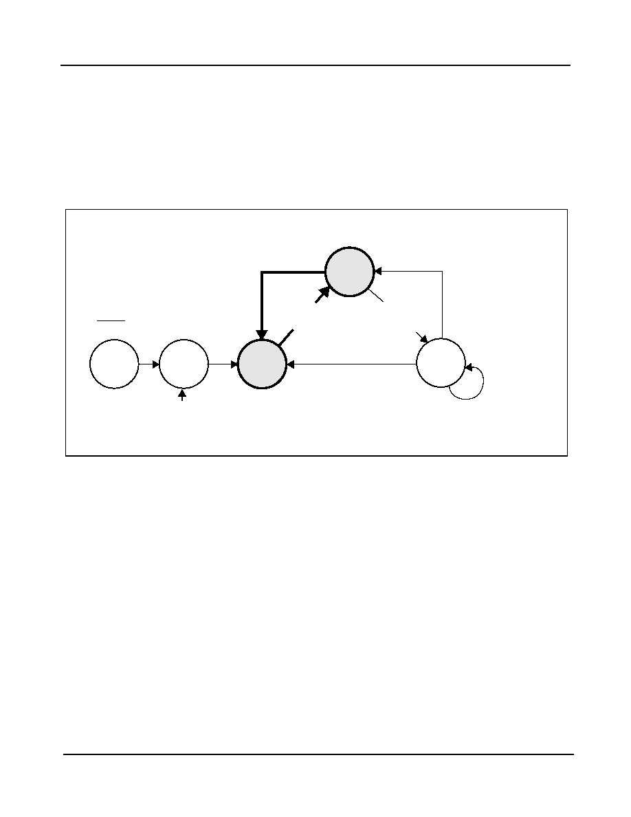
ZL30407
Data Sheet
38
Zarlink Semiconductor Inc.
4.1.5 Reference Switching (RefSel): NORMAL --> HOLDOVER --> NORMAL
The NORMAL to HOLDOVER to NORMAL mode switching is usually performed when:
� A reference clock is available but its frequency drifts beyond some specified limit. In a Network Element with
stratum 3 internal clocks, the reference failure is declared when its frequency drifts more than
�
12 ppm
beyond its nominal frequency. The ZL30407 indicates this condition by setting PRIOR or SECOR status bits
or pins to logic high.
� During routine maintenance of equipment when orderly switching of reference clocks is possible. This may
happen when synchronization references must be rearranged or when a faulty line card must be replaced.
Figure 13 - Manual Reference Switching
Two types of transitions are possible:
� Semi-automatic transition, which involves changing RefSel input to select a secondary reference clock
without changing the mode select inputs MS2, MS1 = 00 (Normal mode). This forces the ZL30407 to
momentarily transition through the Holdover state and automatically return to Normal mode after
synchronizing to a secondary reference clock.
� Manual transition, which involves switching into Holdover mode (MS2,MS1 = 01), changing references with
RefSel, and manual return to the Normal mode (MS2, MS1 = 00).
In both cases, the change of references provides "hitless" switching.
Ref: OK AND
MS2,MS1 = 00
{AUTO}
Ref: OK-->FAIL AND
MS2,MS1 = 00
{AUTO}
MS2,MS1 = 01 OR
RefSel change
MS2,MS1 = 10 forces
unconditional return from
any state to Free-run
RESET = 1
MS2,MS1 = 00
OR
MS2,MS1 = 01
RefSel Change
OR
MS2,MS1 = 01
Ref: FAIL-->OK AND
MS2,MS1 = 00 AND
AHRD = 1 AND MHR = 1
{MANUAL}
Ref: FAIL-->OK AND
MS2,MS1 = 00 AND
AHRD = 0
{AUTO}
OR
AHRD = 1 AND
MHR = 0
RESET
FREE-
RUN
10
HOLD-
OVER
01
NORMAL
00
AUTO
HOLD-
OVER
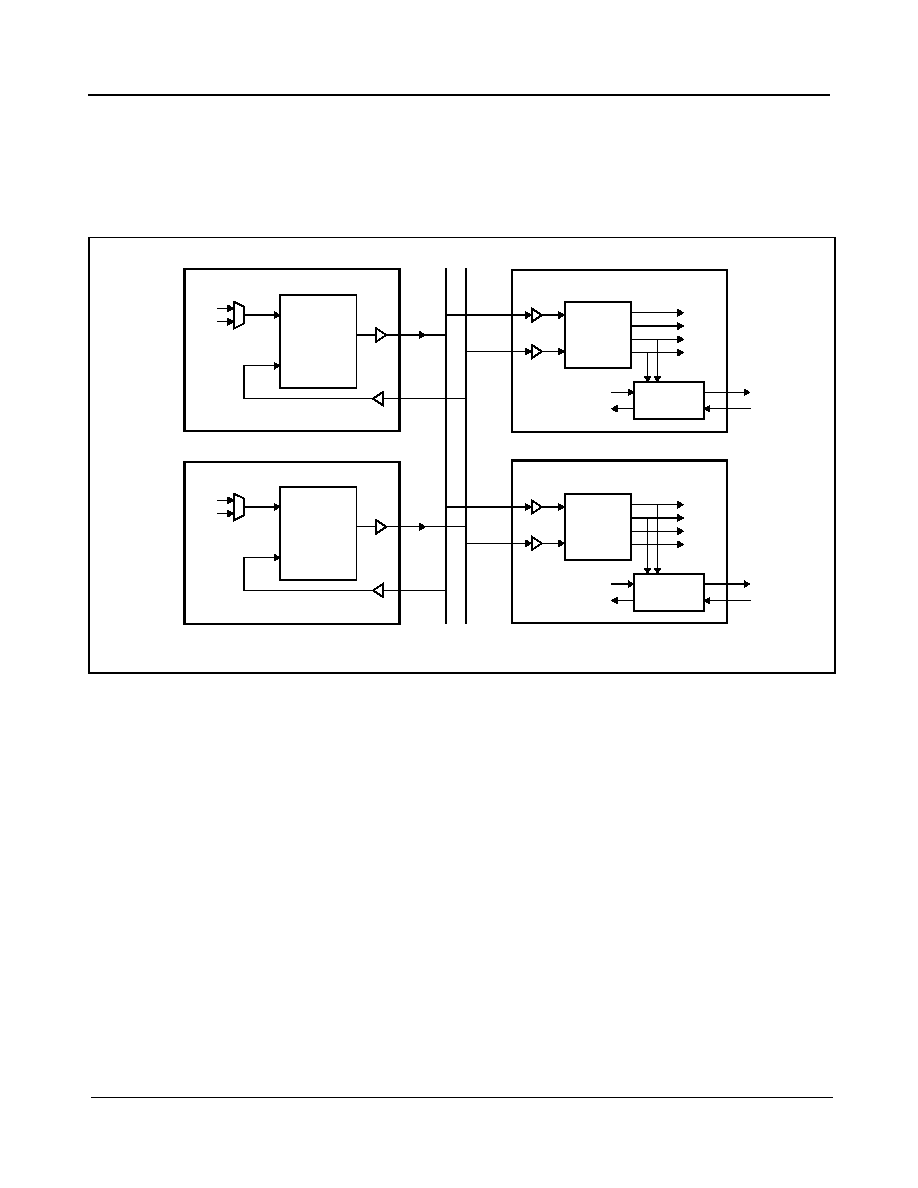
ZL30407
Data Sheet
39
Zarlink Semiconductor Inc.
4.2 Master/Slave Timing Protection Switching
Carrier Class Telecommunications Equipment deployed in today's networks guarantee better than 99.999%
operational availability (equivalent to less than 7 minutes of downtime per year). This high level of uninterrupted
service is achieved by fully redundant architectures with hot swappable cards. Timing for these types of systems
can be generated by the ZL30407 which supports Master/Slave Timing Protection Switching shown in Figure 14.
Figure 14 - Block Diagram of the Master/Slave Timing Protection Switching
The redundant architecture shown in this figure is based on the ZL30407 being deployed on two separate timing
cards; the Master Timing Card and the Slave Timing Card. In normal operation the Master Timing Card receives
synchronization from the network and provides timing for the whole system. All Line Cards in the system are
configured to receive from the backplane a reference clock generated by the Master Timing Card. The redundant
Slave Timing Card is phase locked (through the R3 input) to one of the backplane clocks supplied by the Master
Timing Card. The ZL30407 on the Slave Timing Card is programmed for 12 Hz loop filter operation (FCS2 = 1,
FCS = 0) which allows it to track the Master Timing Card clocks with minimal phase error.
When the Master Timing card fails unexpectedly (this failure is not related to reference failure) then all Line Cards
will detect this failure and they will switch to the timing supplied by the Slave Timing Card. At this moment the
ZL30407 on the Slave Timing Card must be switched from 12 Hz to the same loop filter characteristic (e.g. 1.5 Hz
filter for SDH networks) as the Master Timing Card.
A detailed description of this Master/Slave redundant timing architecture based on ZL30407 can be found in
Application Note ZLAN-67 "Applications of the ZL30407 Master/Slave Application".
ZL30407
SEC
PRI
R0
R1
Timing Card (in Master slot)
ZL30407
SEC
PRI
R0
R1
Timing Card (in Slave slot)
ZL30410
SEC
PRI
Framer
Line Card #m
ZL30410
SEC
PRI
Line Card #n
Backplane
SONET/SDH
with Framers
E3/DS3 MUX
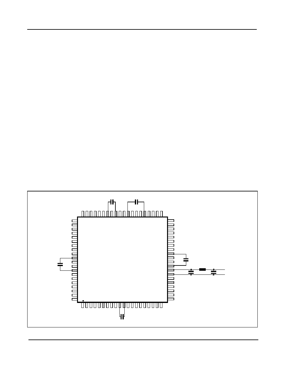
ZL30407
Data Sheet
40
Zarlink Semiconductor Inc.
4.3 Programming Master Clock Oscillator Frequency Calibration Register
The Master Crystal Oscillator and its programmable Master Clock Frequency Calibration register (see Table 19,
Table 20, Table 21, and Table 22) are described in Section 2.5 "Master Clock Frequency Calibration Circuit", on
page 20. Programming of this register should be done after the system has been powered long enough for the
Master Crystal Oscillator to reach a steady operating temperature. When the temperature stabilizes the crystal
oscillator frequency should be measured with an accurate frequency meter. The frequency measurement should be
substituted for the f
offset
variable in the following equation.
MCFC = 45036 * (-f
offset
)
where f
offset
is the crystal oscillator frequency offset from the nominal 20 000 000 Hz frequency expressed in Hz.
Example 1: Calculate the binary value that must be written to the MCFC register to correct a -1 ppm offset of the
Master Crystal Oscillator. The -1 ppm offset for a 20 MHz frequency is equivalent to -20 Hz:
MCFC = 45036 * 20 = 900720 = 00 0D BE 70 H
Note: Correcting the -1 ppm crystal oscillator offset requires +1 ppm MCFC offset.
Example 2: Calculate the binary value that must be written to the MCFC register to correct a +2 ppm offset of the
Master Crystal Oscillator. The +2 ppm offset for 20 MHz frequency is equivalent to 40 Hz:
MCFC = 45036 * (-40) = -1801440 = FF E4 83 20 H
4.4 Power supply filtering
Figure 15 "Power Supply Filtering" presents a complete filtering arrangement that is recommended for applications
requiring maximum jitter performance.
Figure 15 - Power Supply Filtering
ZL30407
40
42
44
46
48
50
52
54
56
58
60
22
24
26
28
30
34
36
38
32
62
80
78
76
74
72
68
66
64
70
20
18
16
14
12
10
8
6
4
2
GND
VDD
AVDD
GND
GND
GN
D
VD
D
GN
D
GND
VDD
VDD
GN
D
VDD
GN
D
VDD
GND
C2
C5
C4
C3
C6
C7
FB
C1
C1, C2, C3, C4, C5 = 0.1 �F (ceramic)
C6, C7 = 1 �F (ceramic)
FB - Ferrite Bead = BLM21A601R (Murrata)
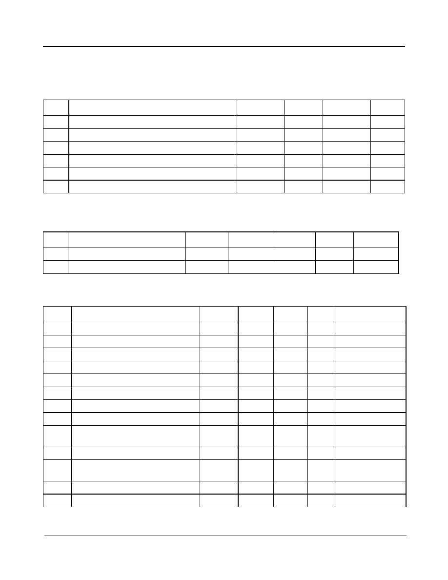
ZL30407
Data Sheet
41
Zarlink Semiconductor Inc.
5.0 Characteristics
5.1 AC and DC Electrical Characteristics
* Voltages are with respect to ground (GND) unless otherwise stated.
* Exceeding these values may cause permanent damage. Functional operation under these conditions is not implied.
* Voltages are with respect to ground (GND) unless otherwise stated.
* Voltages are with respect to ground (GND) unless otherwise stated.
Note 1: VOS is defined as (V
OH
+ V
OL
) / 2.
Note 2: Rise and fall times are measured at 20% and 80% levels.
Absolute Maximum Ratings*
Parameter
Symbol
Min.
Max.
Units
1
Supply voltage
V
DDR
-0.3
7.0
V
2
Voltage on any pin
V
PIN
-0.3
VDD+0.3
V
3
Current on any pin
I
PIN
30
mA
4
Storage temperature
T
ST
-55
125
�
C
5
Package power dissipation (80 pin LQFP)
P
PD
1000
mW
6
ESD rating
V
ESD
1500
V
Recommended Operating Conditions*
Characteristics
Symbol
Min.
Typ.
Max.
Units
1
Supply voltage
V
DD
3.0
3.3
3.6
V
2
Operating temperature
T
A
-40
25
+85
�
C
DC Electrical Characteristics*
Characteristics
Symbol
Min.
Max.
Units
Notes
1
Supply current with C20i = 20 MHz
I
DD
155
mA
Outputs unloaded
2
Supply current with C20i = 0 V
I
DDS
3.5
mA
Outputs unloaded
3
CMOS high-level input voltage
V
CIH
0.7 V
DD
V
4
CMOS low-level input voltage
V
CIL
0.3 V
DD
V
5
Input leakage current
I
IL
15
�
A
V
I
= V
DD
or GND
6
High-level output voltage
V
OH
2.4
V
I
OH
= 10 mA
7
Low-level output voltage
V
OL
0.4
V
I
OL
= 10 mA
8
LVDS: Differential output voltage
V
OD
250
450
mV
Z
T
= 100
9
LVDS: Change in VOD between
complementary output states
dV
OD
50
mV
Z
T
= 100
10
LVDS: Offset voltage
V
OS
1.125
1.375
V
Note 1
11
LVDS: Change in VOS between
complementary output states
dV
OS
50
mV
12
LVDS: Output short circuit current
I
OS
24
mA
Pin short to GND
13
LVDS: Output rise and fall times
T
RF
260
900
ps
Note 2
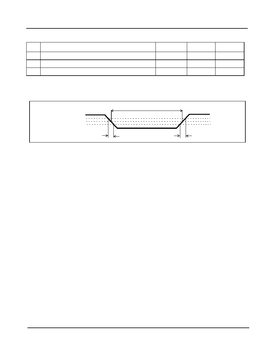
ZL30407
Data Sheet
42
Zarlink Semiconductor Inc.
* Voltages are with respect to ground (GND) unless otherwise stated.
* Supply voltage and operating temperature are as per Recommended Operating Conditions.
* Timing for input and output signals is based on the worst case conditions (over T
A
and V
DD
).
Figure 16 - Timing Parameters Measurement Voltage Levels
AC Electrical Characteristics - Timing Parameter Measurement - CMOS Voltage Levels*
Characteristics
Symbol
Level
Units
1
Threshold voltage
V
T
0.5 V
DD
V
2
Rise and fall threshold voltage High
V
HM
0.7 V
DD
V
3
Rise and fall threshold voltage Low
V
LM
0.3 V
DD
V
ALL SIGNALS
Timing Reference Points
V
HM
V
T
V
LM
t
IF,
t
OF
t
IR,
t
OR
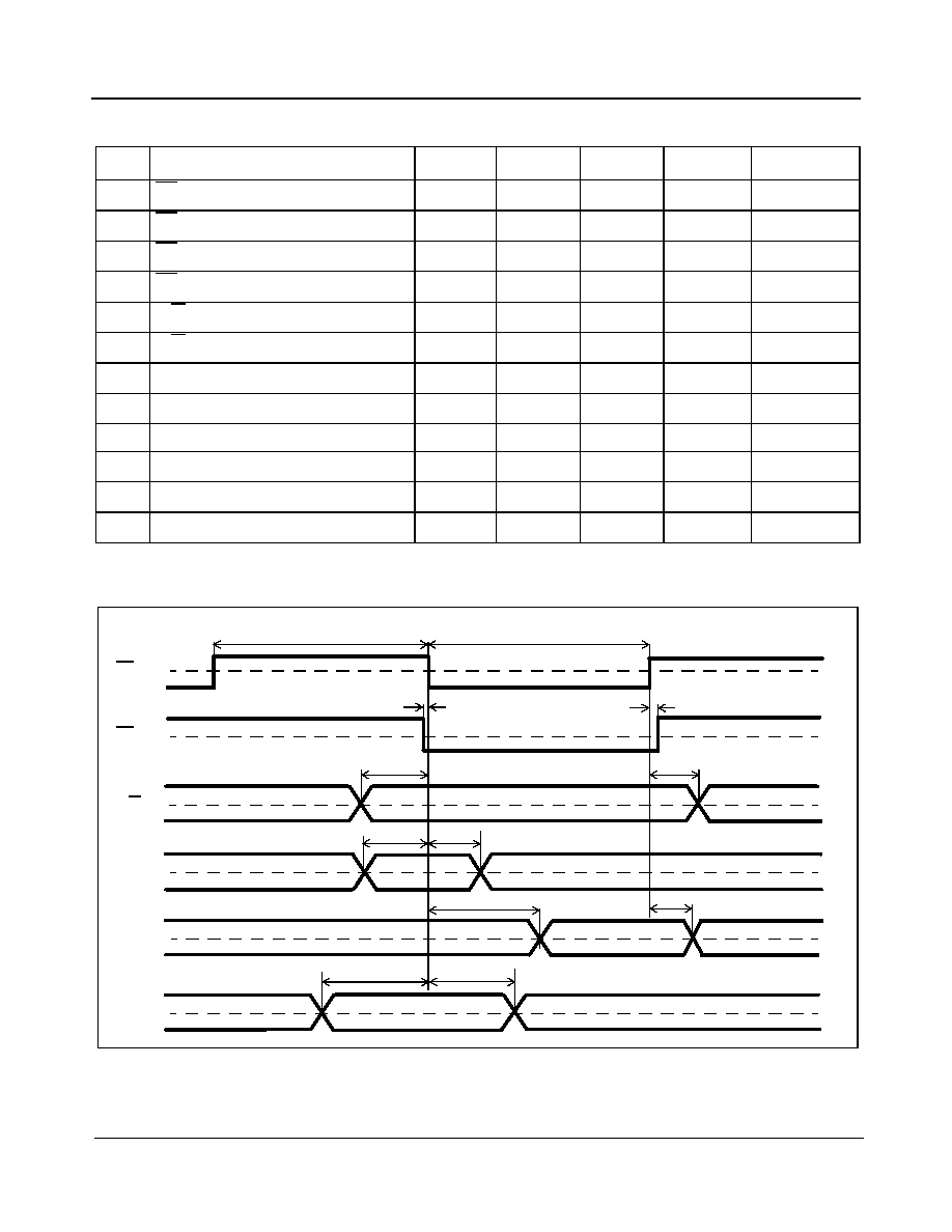
ZL30407
Data Sheet
43
Zarlink Semiconductor Inc.
* Supply voltage and operating temperature are as per Recommended Operating Conditions.
Figure 17 - Microport Timing
AC Electrical Characteristics - Microprocessor Timing*
Characteristics
Symbol
Min.
Max.
Units
Notes
1
DS Low
t
DSL
65
ns
2
DS High
t
DSH
100
ns
3
CS Setup
t
CSS
0
ns
4
CS-Hold
t
CSH
0
ns
5
R/W Setup
t
RWS
20
ns
6
R/W Hold
t
RWH
5
ns
7
Address Setup
t
ADS
10
ns
8
Address Hold
t
ADH
10
ns
9
Data Read Delay
t
DRD
60
ns
C
L
= 90 pF
10
Data Read Hold
t
DRH
10
ns
11
Data Write Setup
t
DWS
10
ns
12
Data Write Hold
t
DWH
5
ns
DS
CS
R/W
A0-A6
D0-D7
READ
D0-D7
WRITE
t
CSS
t
RWS
t
ADS
t
CSH
t
RWH
t
ADH
t
DWS
t
DRD
t
DWH
VALID DATA
t
DSL
V
T
V
T
V
T
V
T
V
T
t
DSH
t
DRH
V
T
VALID DATA
VALID ADDRESS

ZL30407
Data Sheet
44
Zarlink Semiconductor Inc.
* Supply voltage and operating temperature are as per Recommended Operating Conditions.
Figure 18 - ST-BUS and GCI Output Timing
AC Electrical Characteristics - ST-BUS and GCI Output Timing*
Characteristics
Symbol
Min.
Max.
Units
Notes
1
F16o pulse width low (nom 61 ns)
t
F16L
56
62
ns
2
F8o to F16o delay
t
F16D
27
33
ns
3
C16o pulse width low
t
C16L
26
32
ns
4
F8o to C16o delay
t
C16D
-3
3
ns
5
F8o pulse width high (nom 122 ns)
t
F8H
119
125
ns
6
C8o pulse width low
t
C8L
56
62
ns
7
F8o to C8o delay
t
C8D
-3
3
ns
8
F0o pulse width low (nom 244 ns)
t
F0L
241
247
ns
9
F8o to F0o delay
t
F0D
119
125
ns
10
C4o pulse width low
t
C4L
119
125
ns
11
F8o to C4o delay
t
C4D
-3
3
ns
12
C2o pulse width low
t
C2L
240
246
ns
13
F8o to C2o delay
t
C2D
-3
3
ns
t
F16L
t
F16D
t
C16D
V
T
tc = 125
�
s
tc = 61.04 ns
t
F8H
t
C8L
t
C8D
t
F0L
t
F0D
tc = 125
�
s
tc = 122.07 ns
tc = 125
�
s
tc = 244.14 ns
tc = 488.28 ns
t
C4L
t
C4D
t
C2D
t
C2L
F16o
F8o
C16o
C8o
F0o
C4o
C2o
t
C16L
V
T
V
T
V
T
V
T
V
T
V
T
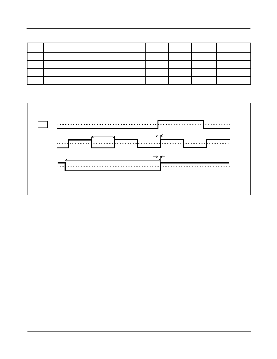
ZL30407
Data Sheet
45
Zarlink Semiconductor Inc.
* Supply voltage and operating temperature are as per Recommended Operating Conditions.
Figure 19 - DS1 and DS2 Clock Timing
AC Electrical Characteristics - DS1 and DS2 Clock Timing*
Characteristics
Symbol
Min.
Max.
Units
Notes
1
C6o pulse width low
t
C6L
75
83
ns
2
F8o to C6o delay
t
C6D
-4
11
ns
3
C1.5o pulse width low
t
C1.5L
320
328
ns
4
F8o to C1.5o delay
t
C1.5D
-4
11
ns
F8o
C6o
C1.5o
tc = 125
�
s
tc = 158.43 ns
t
C6D
V
T
V
T
V
T
t
C1.5L
t
C6L
tc = 647.67 ns
t
C1.5D
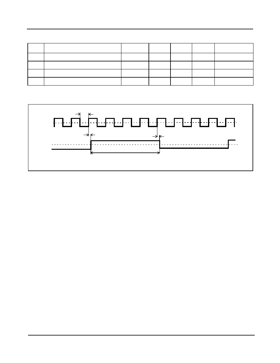
ZL30407
Data Sheet
46
Zarlink Semiconductor Inc.
* Supply voltage and operating temperature are as per Recommended Operating Conditions.
Figure 20 - C155o and C19o Timing
AC Electrical Characteristics - C155o and C19o Clock Timing
Characteristics
Symbol
Min.
Max.
Units
Notes
1
C155o pulse width low
t
C155L
2.6
3.8
ns
2
C155o to C19o rising edge delay
t
C19DLH
-1
7
ns
3
C155o to C19o falling edge delay
t
C19DHL
-2
6
ns
4
C19 pulse width high
t
C19H
23
29
t
C155L
t
C19DLH
t
C19DHL
1.25 V
V
T
tc = 6.43 ns
tc = 51.44 ns
Note: Delay is measured from the rising edge of C155P clock (single ended) at 1.25 V threshold
to the rising and falling edges of C19o clock at V
T
threshold
C155oP
C19o
t
C19H
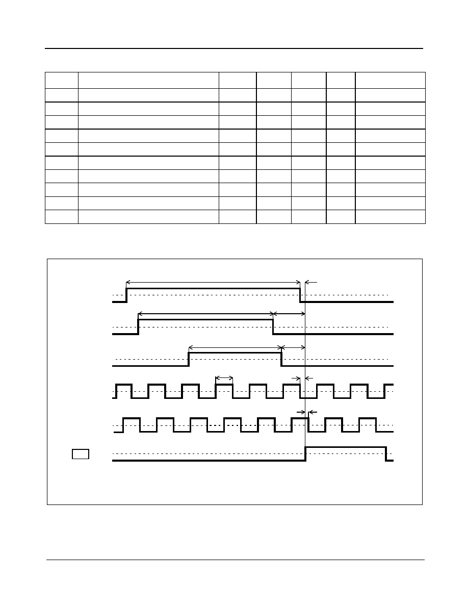
ZL30407
Data Sheet
47
Zarlink Semiconductor Inc.
* Supply voltage and operating temperature are as per Recommended Operating Conditions.
Figure 21 - Input Reference to Output Clock Phase Offset
AC Electrical Characteristics - Input to Output Phase Offset (after phase realignment)*
Characteristics
Symbol
Min.
Max.
Units
Notes
1
8 kHz ref: pulse width high or low
t
R8W
100
ns
2
8 kHz ref input to F8o delay
t
R8D
-6
29
ns
3
1.544 MHz ref: pulse width high or low
t
R1.5W
100
ns
4
1.544 MHz ref input to F8o delay
t
R1.5D
335
350
ns
5
2.048 MHz ref: pulse width high or low
t
R2W
100
ns
6
2.048 MHz ref input to F8o delay
t
R2D
255
272
ns
7
19.44 MHz ref: pulse width high or low
t
R19W
20
ns
8
19.44 MHz ref input to F8o delay
t
R19D
8
21
ns
9
F8o to C19o delay
t
C19D
-5
7
ns
10
Reference input rise and fall time
t
IR
, t
IF
10
ns
t
R8D
t
R1.5D
t
R2D
t
R19D
t
R8W
t
R1.5W
t
R2W
t
R19W
tc = 125
�
s
tc = 647.67 ns
tc = 488.28 ns
tc = 51.44 ns
tc = 51.44 ns
tc = 125
�
s
PRI/SEC
8 kHz
PRI/SEC
1.544 MHz
PRI/SEC
2.048 MHz
PRI/SEC
19.44 MHz
C19o
F8o
V
T
V
T
V
T
V
T
V
T
V
T
Note: Delay time measurements are done with jitter free input reference signals.
t
C19D
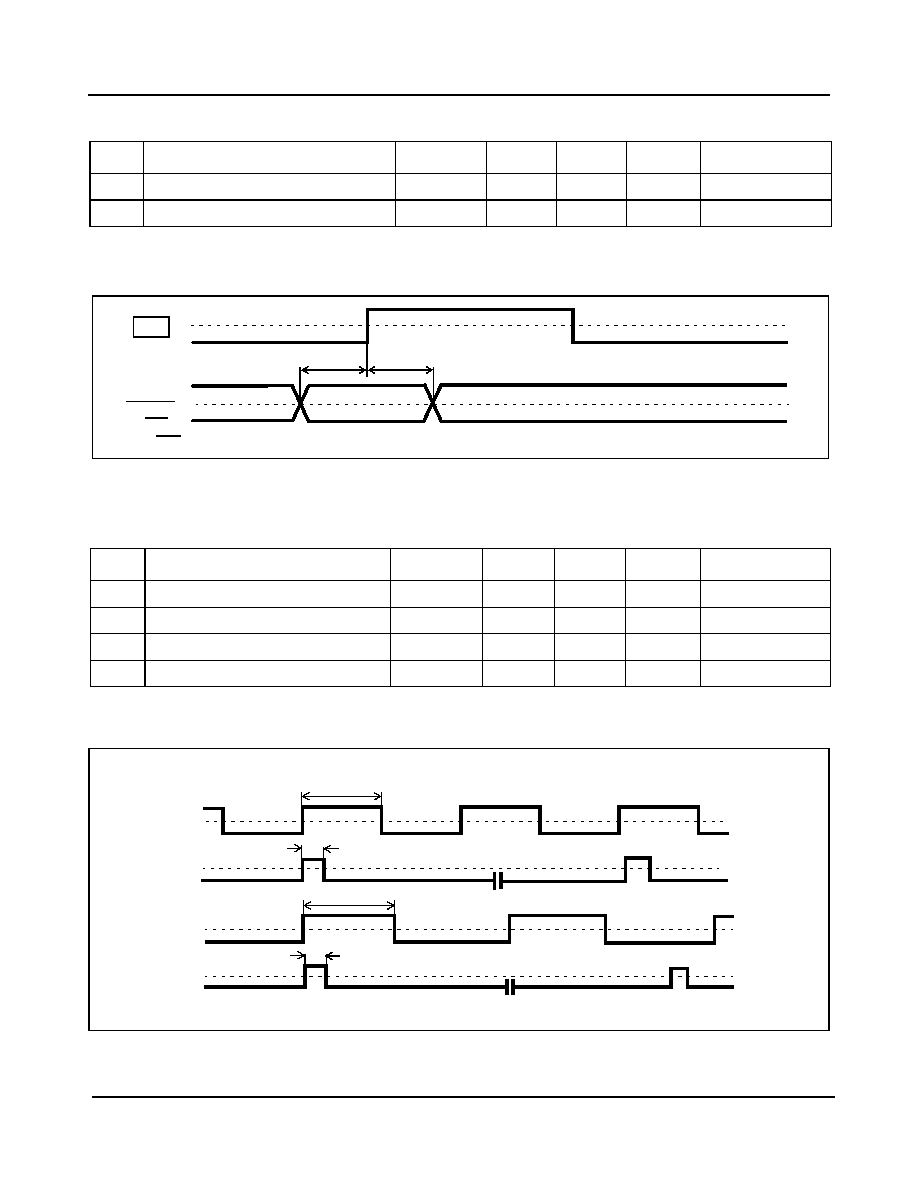
ZL30407
Data Sheet
48
Zarlink Semiconductor Inc.
* Supply voltage and operating temperature are as per Recommended Operating Conditions
Figure 22 - Input Control Signal Setup and Hold Time
* Supply voltage and operating temperature are as per Recommended Operating Conditions.
Figure 23 - E3 and DS3 Output Timing
AC Electrical Characteristics - Input Control Signals*
Characteristics
Symbol
Min.
Max.
Units
Notes
1
Input controls Setup time
t
S
100
ns
2
Input controls Hold time
t
H
100
ns
AC Electrical Characteristics - E3 and DS3 Output Timing*
Characteristics
Symbol
Min.
Max.
Units
Notes
1
C44o clock pulse width high
t
C44H
11
13
ns
2
C11o clock pulse width high
t
C11H
5
26
ns
3
C34o clock pulse width high
t
C34H
13
16
ns
4
C8.5o clock pulse width high
t
C8.5H
9
24
ns
t
S
V
T
V
T
t
H
F8o
MS1, MS2
RefSel, FCS,
RefAlign
E3/DS3
E3DS3/OC3
t
C44H
V
T
t
C34H
t
C8.5H
C44o
tc = 22.35 ns
tc = 89.41 ns
tc = 29.10 ns
tc = 116.39 ns
C11o
C34o
C8.5o
V
T
V
T
V
T
t
C11H

ZL30407
Data Sheet
49
Zarlink Semiconductor Inc.
5.2 Performance Characteristics
Performance Characteristics*
Characteristics
Min.
Typ.
Max.
Units
Notes
1
Holdover accuracy
4x10
-12
7x10
-12
Hz/Hz
0.1 Hz Filter
2
Holdover accuracy
24x10
-12
32x10
-12
Hz/Hz
1.5 Hz Filter
3
Holdover accuracy
70x10
-12
160x10
-12
Hz/Hz
6 Hz Filter
4
Holdover accuracy
140x10
-12
320x10
-12
Hz/Hz
12 Hz Filter
5
Holdover stability
NA
ppm
Holdover stability is
determined by stability of the
20 MHz Master Clock
oscillator
6
Capture range
-104
+104
ppm
The 20 MHz Master Clock
oscillator set at 0ppm
7
Reference Out of Range
Threshold
-12
+12
ppm
The 20 MHz Master Clock
oscillator set at 0 ppm
Lock Time
8
6 Hz or 12 Hz Filter
6
s
�
4.6 ppm frequency offset
9
6 Hz or 12 Hz Filter
6
s
�
20 ppm frequency offset
10
1.5 Hz Filter
20
s
�
4.6 ppm frequency offset
11
0.1 Hz Filter
75
s
�
4.6 ppm frequency offset
12
0.1 Hz Filter
95
s
�
20 ppm frequency offset
Output Phase Continuity
(MTIE)
13
Reference switching:
PRI
SEC, SEC
PRI
50
5
ns
ns
PRI = SEC = 8 kHz
PRI or SEC = 1.544 MHz,
2.048 MHz, 19.44 MHz
14
Switching from Normal
mode to Holdover mode
0
ns
15
Switching from Holdover
mode to Normal mode
50
2
ns
ns
PRI = SEC = 8 kHz
PRI or SEC = 1.544 MHz,
2.048 MHz, 19.44 MHz
(for 0 ppm frequency offset)
Output Phase Slope
16
0.1 Hz Filter
885
ns
sec
G.813 Option 2
GR-253 SONET stratum 3
GR-253 SONET SMC
17
1.5 Hz Filter
41
ns
1.326 ms
G.813 Option 1, GR-1244
stratum 3
ZL30407
Data Sheet
50
Zarlink Semiconductor Inc.
* Supply voltage and operating temperature are as per Recommended Operating Conditions.
Note: See Section 2.2.3 for an explanation of Phase Slope Limiting.
* Supply voltage and operating temperature are as per Recommended Operating Conditions.
* Supply voltage and operating temperature are as per Recommended Operating Conditions.
18
6 Hz Filter
41
ns
1.326 ms
G.813 Option 1
19
12 Hz Filter
150
�
s
sec
Performance Characteristics : Measured Output Jitter - GR-253-CORE and T1.105.03 conformance
Telcordia GR-253-CORE and ANSI T1.105.03
Jitter Generation Requirements
ZL30407 Jitter Generation
Performance
Network
Interface
Jitter
Measurement
Filter
Limit in
UI
Equivalent
limit in
time
domain
Typ.
Units
Notes
C155 Clock Output
1
OC-3
155.52 Mbps
65 kHz to 1.3 MHz
0.15 UIpp
0.964
0.325
ns
P-P
2
12 kHz to1.3 MHz
(Category II)
0.1 UIpp
0.643
0.408
ns
P-P
0.01 UI
RMS
0.064
0.038
ns
RMS
3
500 Hz to 1.3 MHz
1.5 UIpp
9.645
0.448
ns
P-P
C19 Clock Output
4
OC-3
155.52 Mbps
65 kHz to 1.3 MHz
0.15 UIpp
0.964
0.390
ns
P-P
5
12 kHz to1.3 MHz
(Category II)
0.1 UIpp
0.643
0.458
ns
P-P
0.01 UI
RMS
0.064
0.040
ns
RMS
6
500 Hz to 1.3 MHz
1.5 UIpp
9.645
0.512
ns
P-P
Performance Characteristics
: Measured Output Jitter - T1.403 conformance
ANSI T1.403
Jitter Generation Requirements
ZL30407 Jitter Generation
Performance
Network
Interface
Jitter
Measurement
Filter
Limit in
UI
Equivalent
limit in
time
domain
Typ.
Units
Notes
C1.5 Clock Output
1
DS1
1.544 Mbps
8 kHz to 40 kHz
0.07 UIpp
45.3
0.63
ns
P-P
2
10 Hz to 40 kHz
0.5 UIpp
324
0.93
ns
P-P
Performance Characteristics* (continued)
Characteristics
Min.
Typ.
Max.
Units
Notes
ZL30407
Data Sheet
51
Zarlink Semiconductor Inc.
* Supply voltage and operating temperature are as per Recommended Operating Conditions.
* Supply voltage and operating temperature are as per Recommended Operating Conditions.
* Supply voltage and operating temperature are as per Recommended Operating Conditions.
Performance Characteristics
: Measured Output Jitter - G.747 conformance
ITU-T G.747
Jitter Generation Requirements
ZL30407 Jitter Generation
Performance
Network
Interface
Jitter
Measurement
Filter
Limit in
UI
Equivalent
limit in
time
domain
Typ.
Units
Notes
C6 Clock Output
1
DS2
6312 kbps
10 Hz to 60 kHz
0.05 UIpp
7.92
0.53
ns
P-P
Performance Characteristics
: Measured Output Jitter - T1.404 conformance
ANSI T1.403
Jitter Generation Requirements
ZL30407 Jitter Generation
Performance
Network
Interface
Type I
Jitter
Measurement
Filter
Limit in
UI
Equivalent
limit in
time
domain
Typ.
Units
Notes
C44 Clock Output
1
DS3
44.736 Mbps
30 kHz to 400 kHz
0.05 UIpp
1.12
0.30
ns
P-P
2
10 Hz to 400 kHz
0.5 UIpp
11.2
0.47
ns
P-P
Performance Characteristics
: Measured Output Jitter - G.732, G.735 to G.739 conformance
ITU-T G.732, G.735, G.736, G.737, G.738, G.739
Jitter Generation Requirements
ZL30407 Jitter Generation
Performance
Network
Interface
Jitter
Measurement
Filter
Limit in
UI
Equivalent
limit in
time
domain
Typ.
Units
Notes
C16, C8, C4 and C2 Clock Outputs
1
E1
2048 kbps
20 Hz to 100 kHz
0.05 UIpp
24.4
0.56
ns
P-P
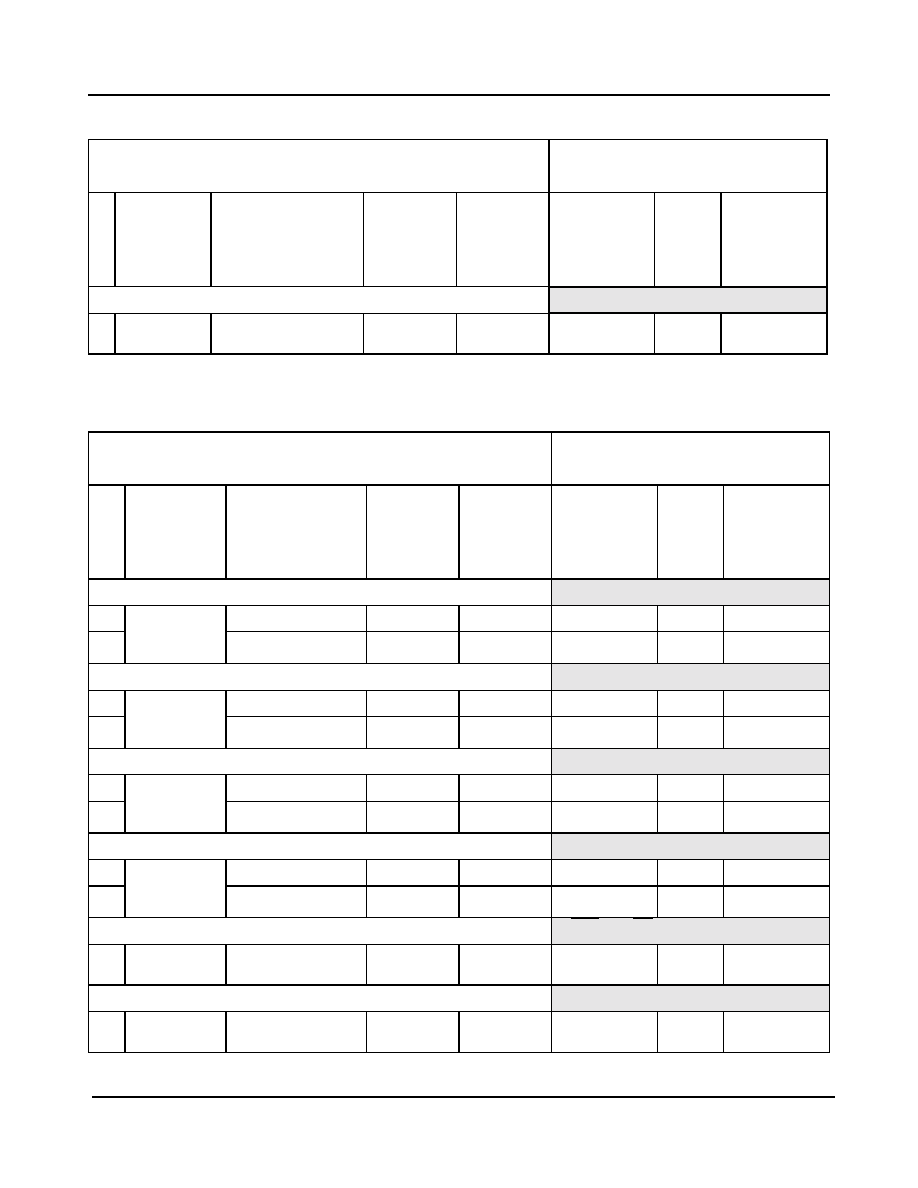
ZL30407
Data Sheet
52
Zarlink Semiconductor Inc.
* Supply voltage and operating temperature are as per Recommended Operating Conditions.
* Supply voltage and operating temperature are as per Recommended Operating Conditions.
Performance Characteristics
: Measured Output Jitter - G.751 conformance
ITU-T G.751
Jitter Generation Requirements
ZL30407 Jitter Generation
Performance
Network
Interface
Jitter
Measurement
Filter
Limit in
UI
Equivalent
limit in
time
domain
Typ.
Units
Notes
C34 Clock Output
1
E3
34368 kbps
100 Hz to 800 kHz
0.05 UIpp
1.45
0.64
ns
P-P
Performance Characteristics
: Measured Output Jitter - G.812 conformance
ITU-T G.812
Jitter Generation Requirements
ZL30407 Jitter Generation
Performance
Network
Interface
Jitter
Measurement
Filter
Limit in
UI
Equivalent
limit in
time
domain
Typ.
Units
Notes
C155 Clock Output
1
STM-1
optical
155.52 Mbps
65 kHz to 1.3 MHz
0.1 UIpp
0.643
0.325
ns
P-P
2
500 Hz to 1.3 MHz
0.5 UIpp
3.215
0.448
ns
P-P
C155 Clock Output
3
STM-1
electrical
155.52 Mbps
65 kHz to 1.3 MHz
0.075 UIpp
0.482
0.325
ns
P-P
4
500 Hz to 1.3 MHz
0.5 UIpp
3.215
0.448
ns
P-P
C19 Clock Output
5
STM-1
optical
155.52 Mbps
65 kHz to 1.3 MHz
0.1 UIpp
0.643
0.390
ns
P-P
6
500 Hz to 1.3 MHz
0.5 UIpp
3.215
0.512
ns
P-P
C19 Clock Output
7
STM-1
electrical
155.52 Mbps
65 kHz to 1.3 MHz
0.075 UIpp
0.482
0.390
ns
P-P
8
500 Hz to 1.3 MHz
0.5 UIpp
3.215
0.512
ns
P-P
C16, C8, C4 and C2 Clock Outputs
9
E1
2048 kbps
20 Hz to 100 kHz
0.05 UIpp
24.4
0.56
ns
P-P
C1.5 Clock Output
10
DS1
1.544 Mbps
10 Hz to 40 kHz
0.05 UIpp
32.4
0.93
ns
P-P
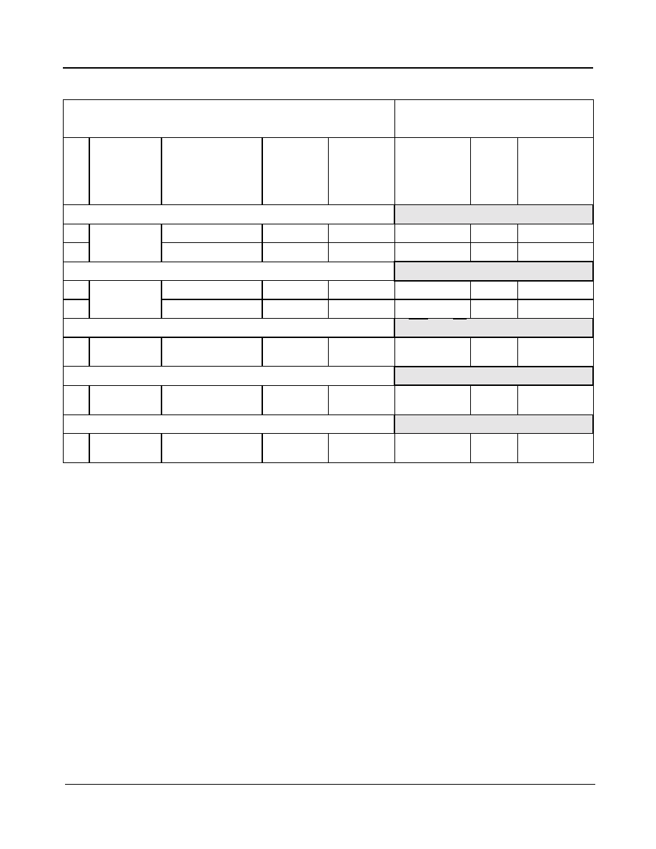
ZL30407
Data Sheet
53
Zarlink Semiconductor Inc.
* Supply voltage and operating temperature are as per Recommended Operating Conditions.
Performance Characteristics
: Measured Output Jitter - G.813 conformance (Option 1 and Option 2)
ITU-T G.813
Jitter Generation Requirements
ZL30407 Jitter Generation
Performance
Interface
Jitter
Measurement
Filter
Limit in
UI
Equivalent
limit in
time
domain
Typ.
Units
Notes
Option 1
C155 Clock Output
1
STM-1
155.52 Mbps
65 kHz to 1.3 MHz
0.1 UIpp
0.643
0.325
ns
P-P
2
500 Hz to 1.3 MHz
0.5 UIpp
3.215
0.448
ns
P-P
C19 Clock Output
3
STM-1
155.52 Mbps
65 kHz to 1.3 MHz
0.1 UIpp
0.643
0.390
ns
P-P
4
500 Hz to 1.3 MHz
0.5 UIpp
3.215
0.512
ns
P-P
C16, C8, C4 and C2 Clock Outputs
5
E1
2048 kbps
20 Hz to 100 kHz
0.05 UIpp
24.4
0.56
ns
P-P
Option 2
C155 Clock Output
6
STM-1
155.52 Mbps
12 kHz to1.3 MHz
0.1 UIpp
0.643
0.408
ns
P-P
C19 Clock Output
7
STM-1
155.52 Mbps
12 kHz to1.3 MHz
0.1 UIpp
0.643
0.458
ns
P-P
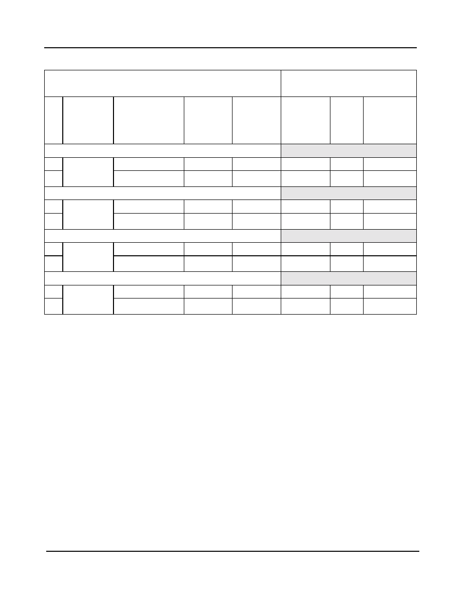
ZL30407
Data Sheet
54
Zarlink Semiconductor Inc.
* Supply voltage and operating temperature are as per Recommended Operating Conditions.
Performance Characteristics
: Measured Output Jitter - EN 300 462-7-1 conformance
ETSI EN 300 462-7-1
Jitter Generation Requirements
ZL30407 Jitter Generation
Performance
Interface
Jitter
Measurement
Filter
Limit in
UI
Equivalent
limit in
time
domain
Typ.
Units
Notes
C155 Clock Output
1
STM-1
optical
155.52 Mbps
65k Hz to 1.3 MHz
0.1 UIpp
0.643
0.325
ns
P-P
2
500 Hz to 1.3 MHz
0.5 UIpp
3.215
0.448
ns
P-P
C155 Clock Output
3
STM-1
electrical
155.52 Mbps
65 kHz to 1.3 MHz
0.075 UIpp
0.482
0.325
ns
P-P
4
500 Hz to 1.3 MHz
0.5 UIpp
3.215
0.448
ns
P-P
C19 Clock Output
5
STM-1
optical
155.52 Mbps
65 kHz to 1.3 MHz
0.1 UIpp
0.643
0.390
ns
P-P
6
500 Hz to 1.3 MHz
0.5 UIpp
3.215
0.512
ns
P-P
C19 Clock Output
7
STM-1
electrical
155.52 Mbps
65 kHz to 1.3 MHz
0.075 UIpp
0.482
0.390
ns
P-P
8
500 Hz to 1.3 MHz
0.5 UIpp
3.215
0.512
ns
P-P
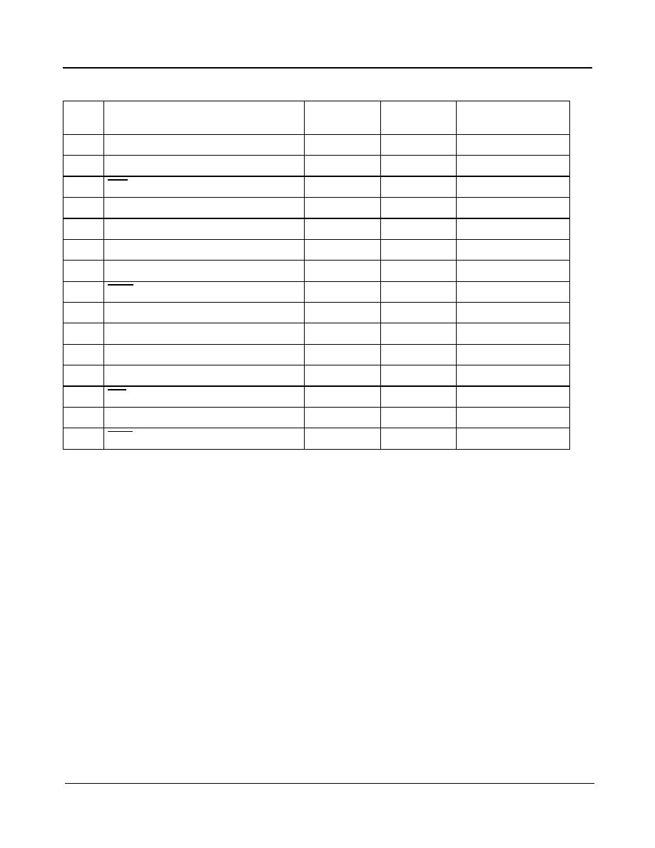
ZL30407
Data Sheet
55
Zarlink Semiconductor Inc.
Performance Characteristics - Measured Output Jitter - Unfiltered*
Characteristics
Typ.
(Ul
PP
)
Typ.
(ns
PP
)
Notes
1
C1.5o (1.544 MHz)
0.0042
2.71
2
C2o (2.048 MHz)
0.0019
0.95
3
C4o (4.096 MHz)
0.0037
0.92
4
C6o (6.312 MHz)
0.0179
2.84
5
C8o (8.192 MHz)
0.0081
0.99
6
C8.5o (8.592 MHz)
0.0222
2.58
7
C11o (11.184 MHz)
0.0295
2.64
8
C16o (16.384 MHz)
0.0161
0.98
9
C19o (19.44 MHz)
0.0125
0.64
10
C34o (34.368 MHz)
0.0433
1.26
11
C44o (44.736 MHz)
0.0546
1.22
12
C155o (155.52 MHz)
0.0867
0.56
13
F0o (8 kHz)
NA
0.44
14
F8o (8 kHz)
NA
0.46
15
F16o (8 kHz)
NA
0.45


www.zarlink.com
Information relating to products and services furnished herein by Zarlink Semiconductor Inc. or its subsidiaries (collectively "Zarlink") is believed to be reliable.
However, Zarlink assumes no liability for errors that may appear in this publication, or for liability otherwise arising from the application or use of any such
information, product or service or for any infringement of patents or other intellectual property rights owned by third parties which may result from such application or
use. Neither the supply of such information or purchase of product or service conveys any license, either express or implied, under patents or other intellectual
property rights owned by Zarlink or licensed from third parties by Zarlink, whatsoever. Purchasers of products are also hereby notified that the use of product in
certain ways or in combination with Zarlink, or non-Zarlink furnished goods or services may infringe patents or other intellectual property rights owned by Zarlink.
This publication is issued to provide information only and (unless agreed by Zarlink in writing) may not be used, applied or reproduced for any purpose nor form part
of any order or contract nor to be regarded as a representation relating to the products or services concerned. The products, their specifications, services and other
information appearing in this publication are subject to change by Zarlink without notice. No warranty or guarantee express or implied is made regarding the
capability, performance or suitability of any product or service. Information concerning possible methods of use is provided as a guide only and does not constitute
any guarantee that such methods of use will be satisfactory in a specific piece of equipment. It is the user's responsibility to fully determine the performance and
suitability of any equipment using such information and to ensure that any publication or data used is up to date and has not been superseded. Manufacturing does
not necessarily include testing of all functions or parameters. These products are not suitable for use in any medical products whose failure to perform may result in
significant injury or death to the user. All products and materials are sold and services provided subject to Zarlink's conditions of sale which are available on request.
Purchase of Zarlink's I
2
C components conveys a licence under the Philips I
2
C Patent rights to use these components in and I
2
C System, provided that the system
conforms to the I
2
C Standard Specification as defined by Philips.
Zarlink, ZL and the Zarlink Semiconductor logo are trademarks of Zarlink Semiconductor Inc.
Copyright Zarlink Semiconductor Inc. All Rights Reserved.
TECHNICAL DOCUMENTATION - NOT FOR RESALE
For more information about all Zarlink products
visit our Web Site at