Document Outline
- Features
- Applications
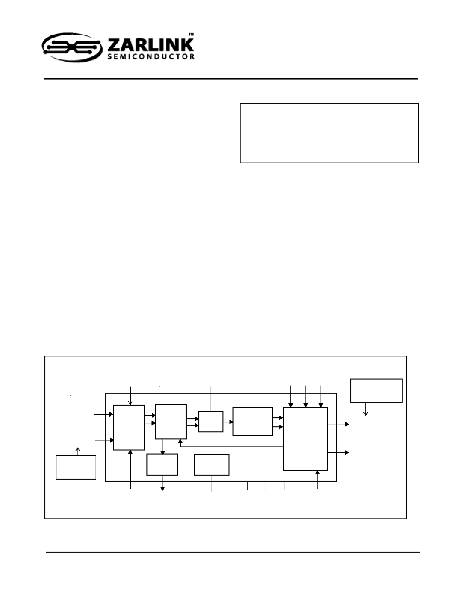
- Figure 1 - Functional Block Diagram
- Description
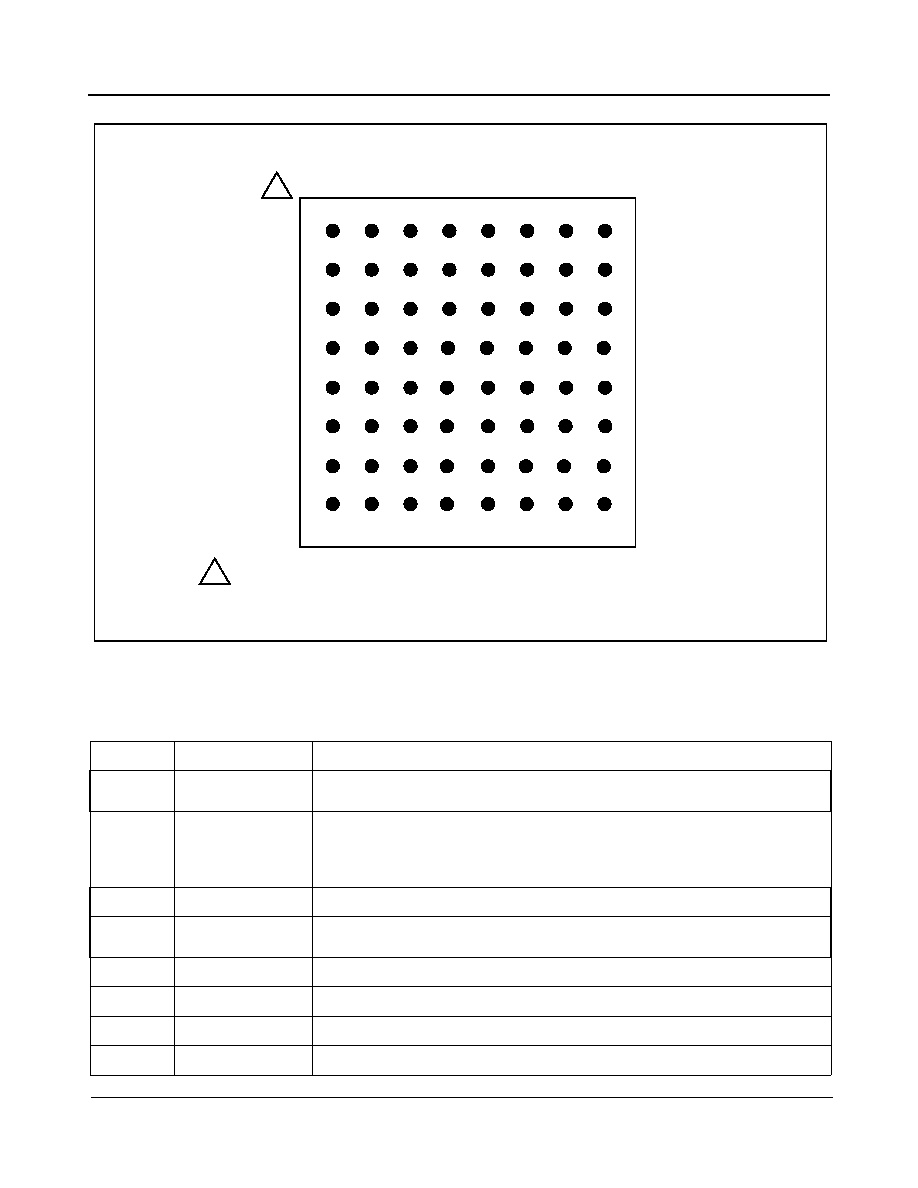
- Figure 2 - BGA 64 Ball Package (Top View)
- 1.0 Ball Description
- 2.0 Functional Description
- 2.1 Reference Selection Multiplexer
- Table 1 - Input Reference Selection
- 2.2 Frequency/Phase Detector
- 2.3 Lock Indicator
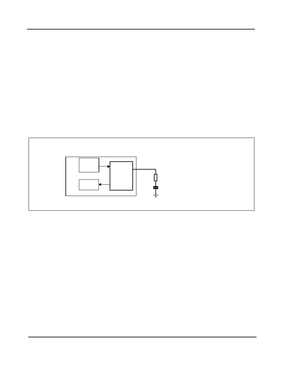
- 2.4 Loop Filter
- Figure 3 - Loop Filter Elements
- 2.5 VCO
- 2.6 Frequency Dividers and Clock Drivers
- Table 2 - OC-CLKo Clock Frequency Selection
- 3.0 ZL30416 Performance
- 3.1 Input Jitter Tolerance
- Figure 4 - Input Jitter Tolerance
- 3.2 Jitter Transfer Characteristic
- 4.0 Applications
- 4.1 Generation of Low Jitter SONET/SDH Equipment Clocks
- Figure 5 - SONET/SDH Equipment Clock
- 4.2 Recommended Interface Circuit
- 4.2.1 Interfacing to REFin Receiver
- 4.2.1.1 Interfacing REFin Receiver to LVPECL Driver
- Figure 6 - Interfacing to LVPECL Driver
- 4.2.1.2 Interfacing REFin Receiver to LVDS or CML Drivers
- Figure 7 - Interfacing to LVDS or CML Driver
- 4.2.2 Interfacing to OC-CLKo Output
- 4.2.2.1 LVPECL to LVPECL Interface
- Figure 8 - LVPECL to LVPECL Interface
- 4.3 Power supply and BIAS Circuit Filtering Recommendations
- Figure 9 - Power Supply and BIAS Circuit Filtering
- 5.0 Characteristics
- Absolute Maximum RatingsÅ
- Recommended Operating ConditionsÅ
- DC Electrical Characteristics�
- AC Electrical Characteristics�- Output Timing Parameters Measurement Voltage Levels
- Figure 10 - Output Timing Parameter Measurement Voltage Levels
- AC Electrical Characteristics�- C19i Input to C19o Output Timing
- Figure 11 - C19i Input to C19o Output Timing
- AC Electrical CharacteristicsÅ - REFin to C19o Output Timings
- Figure 12 - REFin Input to C19o Output Timing
- Figure 13 - C19i Input to OC-CLKo Output Timing
- Figure 14 - REFin (19.44�MHz) Input to OC-CLKo Output Timing
- Figure 15 - REFin (77.76�MHz) Input to OC-CLKo Output Timing
- Performance Characteristics - Functional - (VCC = 3.3�V ±10%; TA = -40 to 85∞C)
- Performance Characteristics: Output Jitter Generation - GR-253-CORE conformance (VCC = 3.3�V ±10%...
- Performance Characteristics: Output Jitter Generation - G.813 conformance (Option 1 and 2) (VCC =...
- Performance Characteristics: Output Jitter Generation - ETSI EN 300 462-7-1conformance (VCC = 3.3...
1
Zarlink Semiconductor Inc.
Zarlink, ZL and the Zarlink Semiconductor logo are trademarks of Zarlink Semiconductor Inc.
Copyright 2004, Zarlink Semiconductor Inc. All Rights Reserved.
Features
∑ Low jitter clock outputs suitable for OC-192, OC-
48, OC-12, OC-3 and OC-1 SONET applications
as defined in Telcordia GR-253-CORE
∑ Low jitter clock outputs suitable for STM-64, STM-
16, STM-4 and STM-1 applications as defined in
ITU-T G.813
∑ Provides one differential LVPECL output clock
selectable to 19.44, 38.88, 77.76, 155.52 or
622.08 MHz
∑ Provides a single-ended CMOS output clock at
19.44 MHz
∑ Accepts a single-ended CMOS reference at
19.44 MHz or a differential LVDS, LVPECL or
CML reference at 19.44 or 77.76 MHz
∑ Provides a LOCK indication
∑ 8 mm x 8 mm CABGA package
∑ 3.3 V supply
Applications
∑ SONET/SDH line cards
Description
The ZL30416 is an Analog Phase-Locked Loop (APLL)
designed to provide jitter attenuation and rate
conversion for SDH (Synchronous Digital Hierarchy)
and SONET (Synchronous Optical Network)
networking equipment. The ZL30416 generates low
jitter output clocks suitable for Telcordia GR-253-
CORE OC-192, OC-48, OC-12, OC-3, and OC-1 and
ITU-T G.813 STM-64, STM-16, STM-4 and STM-1
applications.
The ZL30416 accepts a CMOS compatible reference
at 19.44 MHz or a differential LVDS, LVPECL or CML
reference at 19.44 or 77.76 MHz and generates a
differential LVPECL output clock selectable to 19.44,
38.88, 77.76, 155.52 or 622.08 MHz and a single-
ended CMOS clock at 19.44 MHz. The ZL30416
provides a lock indication.
November 2004
Ordering Information
ZL30416GGG 64 Ball CABGA
-40
∞
C to +85
∞
C
ZL30416
SONET/SDH Clock Multiplier PLL
Data Sheet
Figure 1 - Functional Block Diagram
Frequency
Detector
VCO
Frequency
LPF
OC-CLKoP/N
VCC
GND
VDD
C19o
FS2
Loop
Filter
BIAS
& Phase
19.44 MHz and 77.76 MHz
State
Machine
LOCK
Reference
Bias Circuit
and
Dividers
and
Clock
Drivers
C19o, C38o, C77o,
C155o, C622o,
LVPECL output
C19i
Reference
Selection
MUX
REF_SEL
REF_FREQ
REFinP/N
C19oEN
C19i or C77i
CML, LVDS,
LVPECL input
FS3
FS1
ZL30416
Data Sheet
2
Zarlink Semiconductor Inc.
Figure 2 - BGA 64 Ball Package (Top View)
1.0 Ball Description
Ball Description Table
Ball
#
Name
Description
A1, A2
A3
NC
No internal bonding Connection. Leave unconnected.
A4
A5
OC-CLKoP
OC-CLKoN
SONET/SDH Clock (LVPECL Output). These outputs provide a selectable
differential LVPECL clock at 19.44 Hz, 38.88 MHz, 77.76 MHz, 155.52 MHz,
and 622.08 MHz. The output frequency is selected with FS3, FS2 and FS1
inputs.
A6
GND
Ground. 0 volt
A7, A8
B1, B2
NC
No internal bonding Connection. Leave unconnected.
B3
VCC1
Positive Analog Power Supply. +3.3 V +/-10%
B4
GND
Ground. 0 volt
B5
NC
No internal bonding Connection. Leave unconnected.
B6, B7
GND
Ground. 0 volt
B
C
D
E
F
G
H
1
2
3
4
5
6
7
8
1
1 - A1 corner is identified by metallized markings.
A
LOCK
VCC2
NC
NC REF_FREQ
NC
NC
NC
VDD
VDD
GND
C19o
VCC
VDD
REF_SEL
GND
GND
VCC
VCC
BIAS
GND
GND
REFinP
FS1
FS2
GND
FS3
VCC
GND
C19i
GND
NC
GND
GND
OC-CLKoP OC-CLKoN GND
GND
NC
NC
VCC1
NC
NC
GND
LPF
GND
GND
GND
GND
NC
REFinN
VDD
VDD
C19oEN
NC
NC
VDD
VDD
8 mm x 8 mm
Ball Pitch 0.8mm
NC
NC
NC
NC
GND
NC
ZL30416
Data Sheet
3
Zarlink Semiconductor Inc.
B8
VCC
Positive Analog Power Supply. +3.3 V ±10%
C1
GND
Ground. 0 volt
C2
VCC2
Positive Analog Power Supply. +3.3 V ±10%
C3, C4
C5
GND
Ground. 0 volt
C6
NC
No internal bonding Connection. Leave unconnected.
C7
VDD
Positive Digital Power Supply. +3.3 V ±10%
C8
GND
Ground. 0 volt
D1
BIAS
Bias Circuit.
D2
LPF
External Low-Pass Filter (Analog). Connect external RC network for the low-
pass filter.
D3
NC
No internal bonding Connection. Leave unconnected.
D4
GND
Ground. 0 volt
D5, D6
VCC
Positive Analog Power Supply. +3.3 V ±10%
D7, D8
GND
Ground. 0 volt
E1
LOCK
Lock Indicator (CMOS Output). This output goes high when the PLL is
frequency locked to the selected input reference.
E2, E3
NC
No internal bonding Connection. Leave unconnected.
G4
E4
H5
FS3
FS2
FS1
Frequency Select 3-1 (CMOS Input). These inputs select the clock frequency
on the OC-CLKo output. The possible output frequencies are:
19.44 MHz (000), 38.88 MHz (001), 77.76 MHz (010), 155.52 MHz (011),
622.08 (100)
E5
VCC
Positive Analog Power Supply. +3.3 V ±10%
E6
VDD
Positive Digital Power Supply. +3.3 V ±10%
E7
NC
No internal bonding Connection. Leave unconnected.
E8
F8
REFinN
REFinP
Differential Reference Clock Input (CML/LVDS/LVPECL Compatible Input).
These inputs accept a differential clock at 77.76 MHz or 19.44 MHz as the
reference for synchronization. These inputs do not have on-chip AC coupling
capacitors.
F1, F2
NC
No internal bonding Connection. Leave unconnected.
F3
REF_FREQ
Reference Frequency (CMOS Input). This input selects the rate of the
differential input clock (REFinP/N) to be either 77.76 MHz or 19.44 MHz.
F4
C19oEN
C19o Output Enable (CMOS Input). If tied high this control input enables the
C19o output clock. Pulling this pin low forces the output driver into a high
impedance state.
F5
C19i
C19 Reference Input (CMOS Input). This is a single-ended input reference
source used for synchronization. This input accepts 19.44 MHz.
Ball Description Table (continued)
Ball
#
Name
Description

ZL30416
Data Sheet
4
Zarlink Semiconductor Inc.
2.0 Functional Description
The ZL30416 is an analog phased-locked loop which provides rate conversion and jitter attenuation for
SONET/SDH OC-192/STM-64, OC-48/STM-16, OC-12/STM-4 and OC-3/STM-1 applications. A functional block
diagram of the ZL30416 is shown in Figure 1 and a brief description is presented in the following sections.
2.1 Reference Selection Multiplexer
The ZL30416 accepts two types of input reference clocks:
- differential: operating at 19.44 MHz or 77.76 MHz, compatible with LVDS/LVPECL/CML threshold levels
- single-ended: operating at 19.44 MHz, compatible with CMOS switching levels
The REF_SEL input determines whether the single-ended CMOS reference input (REFin) or the differential
reference inputs (REFinP/N) are used as input reference clocks. The REF_FREQ input selects the rate of the
differential input clock to be either 19.44 MHz or 77.76 MHz. See Table 1 for details.
F6
C19o
Clock 19.44 MHz (CMOS Output). This output provides a single-ended CMOS
clock at 19.44 MHz.
F7, G1
GND
Ground. 0 volt
G2
VDD
Positive Digital Power Supply. +3.3 V ±10%
G3
REF_SEL
Reference Select (CMOS Input). If tied low then the C19i single-ended
reference is used as the input reference source. If tied high then the REFinP/N
differential pair is used as the input reference source.
G4
FS3
See E4 ball description.
G5, G6
GND
Ground. 0 volt
G7, G8
VDD
Positive Digital Power Supply. +3.3 V ±10%
H1, H2
H3
NC
No internal bonding Connection. Leave unconnected.
H4
VDD
Positive Digital Power Supply. +3.3 V ±10%
H5
FS1
See E4 ball description.
H6
VDD
Positive Digital Power Supply. +3.3 V ±10%
H7, H8
GND
Ground. 0 volt.
REF_SEL
REF_FREQ
Selected Input Reference
Reference Frequency
0
x
C19i
19.44 MHz (CMOS)
1
0
REFin
77.76 MHz (Differential)
1
1
REFin
19.44 MHz (Differential)
Table 1 - Input Reference Selection
Ball Description Table (continued)
Ball
#
Name
Description
ZL30416
Data Sheet
5
Zarlink Semiconductor Inc.
2.2 Frequency/Phase Detector
The Frequency/Phase Detector compares the frequency/phase of the input reference signal with the feedback
signal from the Frequency Divider circuit and provides an error signal equal to the frequency/phase
difference between the two. This error signal is passed to the Loop Filter circuit.
2.3 Lock Indicator
The ZL30416 has a built-in LOCK detector that measures frequency difference between input reference clock C19i
and the VCO frequency. When the VCO frequency is less than
±
300 ppm apart from the input reference frequency
then the LOCK output is set high. The LOCK output is pulled low if the frequency difference exceeds
±
1000 ppm.
2.4 Loop Filter
The Loop Filter is a low-pass filter. This low-pass filter eliminates high frequency spectral components from a phase
error signal produced by the Phase Detector. This ensures low output jitter that meets network jitter requirements.
The corner frequency of the Loop Filter is configurable with an external capacitor and resistor connected to the LPF
ball and ground as shown in Figure 3.
Figure 3 - Loop Filter Elements
2.5 VCO
The voltage-controlled oscillator (VCO) receives the filtered error signal from the Loop Filter and based on the
voltage of the error signal generates a primary frequency. The VCO output is connected to the "Frequency Dividers
and Clock Drivers" block that divides VCO frequency and buffer generated clocks.
R
F
C
F
ZL30416
LPF
R
F
=8.2 k
,
C
F
=470 nF
Filter
Loop
Frequency
and Phase
Detector
VCO
f
TYP
=14.4 kHz

ZL30416
Data Sheet
6
Zarlink Semiconductor Inc.
2.6 Frequency Dividers and Clock Drivers
The output of the VCO feeds the high frequency clock to the "Frequency Dividers and Clock Drivers" circuit to
provide one differential LVPECL compatible clock with selectable frequency and one single-ended 19.44 MHz C19o
output clock. The C19o clock can be enabled or disabled with the associated C19oEN Output Enable ball.
Internally, this block provides a feedback clock that closes the PLL loop.
The frequency of the OC-CLKo differential output clock is selected with FS3, FS2 and FS1 inputs as is shown in the
following table.
FS3
FS2
FS1
OC-CLKo
Frequency
0
0
0
19.44 MHz
0
0
1
38.88 MHz
0
1
0
77.76 MHz
0
1
1
155.52 MHz
1
0
0
622.08 MHz
1
0
1
Reserved
1
1
0
Reserved
1
1
1
Reserved
Table 2 - OC-CLKo Clock Frequency Selection
ZL30416
Data Sheet
7
Zarlink Semiconductor Inc.
3.0 ZL30416 Performance
The following are some of the ZL30416 performance indicators that complement results listed in the Characteristics
section of this data sheet.
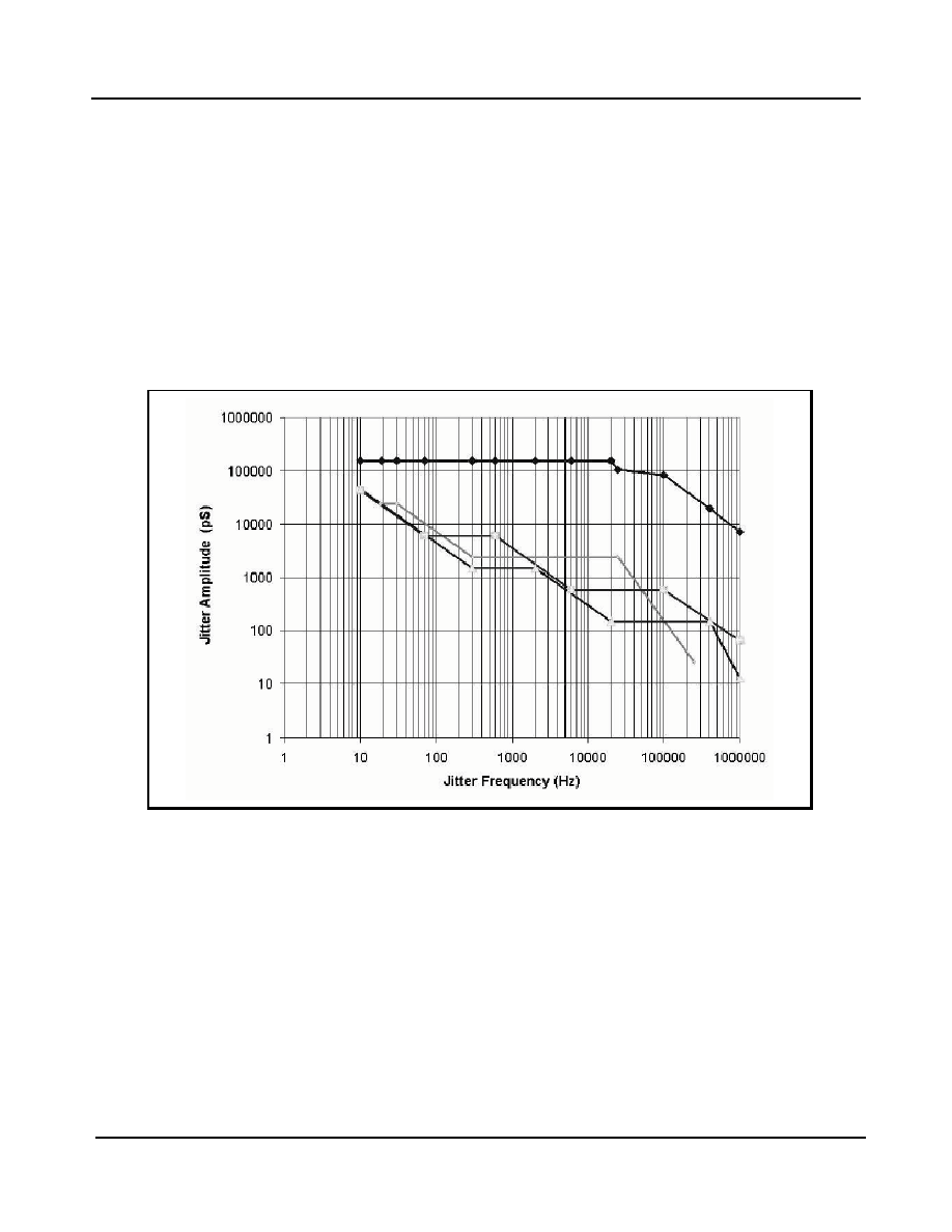
3.1 Input Jitter Tolerance
Jitter tolerance is a measure of the PLL's ability to operate properly (i.e., remain in lock and/or regain lock in the
presence of large jitter magnitudes at various jitter frequencies) in the presence of jitter applied to its input
reference. The input jitter tolerance of the ZL30416 is shown in Figure 4. On this graph, the single line at the top
represents the input jitter tolerance and the three overlapping lines below represent the specification for minimum
input jitter tolerance for OC-192, OC-48 and OC-12 network interfaces. The jitter tolerance is expressed in
picoseconds (pk-pk) to accommodate requirements for interfaces operating at different rates.
Figure 4 - Input Jitter Tolerance
3.2 Jitter Transfer Characteristic
Jitter Transfer Characteristic represents a ratio of the jitter at the output of a PLL to the jitter applied to the input of a
PLL. This ratio is expressed in dB and it characterizes the PLL's ability to attenuate (filter) jitter. The ZL30416 jitter
transfer characteristic complies with the maximum 0.1 dB jitter gain specified in Telcordia's GR-253-CORE.
ZL30416
Data Sheet
8
Zarlink Semiconductor Inc.
4.0 Applications
4.1 Generation of Low Jitter SONET/SDH Equipment Clocks
The functionality and performance of the ZL30416 complements the entire family of the Zarlink's advanced network
synchronization PLL's. Its jitter filtering characteristics exceed requirements of SONET/SDH optical interfaces
operating up to OC-192/STM-64. The ZL30416 in combination with the MT90401 or the ZL30407 (SONET/SDH
Network Element PLL's) provides the core building blocks for high quality equipment clocks suitable for network
synchronization (see Figure 5).
Figure 5 - SONET/SDH Equipment Clock
ZL30416
38.88 MHz
19.44 MHz
OC-CLKoP/N LVPECL
C19o CMOS
C19i
C19o CMOS
C155o LVDS
C34o/C44o CMOS
C16o CMOS
C8o CMOS
C6o CMOS
19.44 MHz
C2o CMOS
C1.5o CMOS
F8o CMOS
F0o CMOS
77.76 MHz
19.44 MHz
622.08 MHz
155.52 MHz
C4o CMOS
34.368 MHz or 44.736 MHz
16.384 MHz
8.192 MHz
6.312 MHz
4.096 MHz
2.048 MHz
1.544 MHz
8 kHz
8 kHz
PRI
SEC
PRIOR
SECOR
LOCK
HOLDOVER
RefSel
RefAlign
R
F
LPF
C
F
F
S
1
155.52 MHz
R
E
F
_
S
E
L
R
E
F
_
F
R
E
Q
F
S
3
F
S
2
C
1
9
o
E
N
D
S
C
S
R
/
W
A
0
-
A
6
D
0
-
D
7
uP
Data Port
Controller Port
Synchronization
Reference
Clocks
Note: Only main functional connections are shown
20 MHz
C
2
0
i
F16o CMOS
OCXO
8 kHz
ZL30407
L
O
C
K
REFinP/N
R
F
= 1 k
C
F
= 470 nF

ZL30416
Data Sheet
9
Zarlink Semiconductor Inc.
4.2 Recommended Interface Circuit
4.2.1 Interfacing to REFin Receiver
4.2.1.1 Interfacing REFin Receiver to LVPECL Driver
The ZL30416 REFin differential receiver can be connected to LVPECL compatible driver with an interface circuit, as
shown in Figure 7. The R1s and R2s terminating resistors should be placed close to the REFin input balls.
Figure 6 - Interfacing to LVPECL Driver
4.2.1.2 Interfacing REFin Receiver to LVDS or CML Drivers
The ZL30416 REFin differential receiver can be connected to LVDS or CML driver with an interface circuit, as
shown in Figure 7. The 100
terminating resistors should be placed close to the REFin input balls.
Figure 7 - Interfacing to LVDS or CML Driver
LVPECL
Z=50
Z=50
Typical resistor values: R1 = 127
, R2 =82.5
Typical capacitor values: Cc = 0.1
µ
F
R1
VCC=+3.3V
R1
Driver
ZL30416
Receiver
Cc
VDD/2
Cc
REFinP
REFinN
R2
R2
ZL30416
Z=50
Driver
Receiver
Z=50
Cc
VDD/2
LVDS
Cc
100
REFinP
REFinN
or
CML
Typical capacitor values: Cc = 0.1
µ
F
ZL30416
Data Sheet
10
Zarlink Semiconductor Inc.
4.2.2 Interfacing to OC-CLKo Output
4.2.2.1 LVPECL to LVPECL Interface
The OC-CLKo outputs provide differential LVPECL clocks at 622.08 MHz, 155.52 MHz, 77.76 MHz, 38.88 MHz and
19.44 MHz selectable with FS3, FS2 and FS1 frequency select inputs. The LVPECL output drivers require a 50
termination connected to the Vcc-2V source for each output terminal at the terminating end as shown below. The
terminating resistors should be placed close to the LVPECL receiver.
Figure 8 - LVPECL to LVPECL Interface
LVPECL
LVPECL
ZL30416
Z=50
Z=50
OC-CLKoP
OC-CLKoN
Receiver
GND
Typical resistor values: R1 = 127
, R2 =82.5
R1
R2
VCC=+3.3 V
R1
R2
VCC
0.1 uF
+3.3 V
Driver
ZL30416
Data Sheet
11
Zarlink Semiconductor Inc.
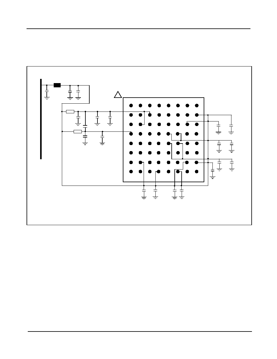
4.3 Power supply and BIAS Circuit Filtering Recommendations
Figure 9 presents a complete filtering arrangement that is recommended for applications requiring maximum jitter
performance. The level of required filtering is subject to further optimization and simplification. Please check
Zarlink's web site for updates.
Figure 9 - Power Supply and BIAS Circuit Filtering
Notes:
1. All the ground pins (GND) are connected to the same ground plane.
2. Select Ferrite Bead with I
DC
> 400 mA and R
DC
in a range from 0.10
to 0.15
.
B
C
D
E
F
G
H
1
2
3
4
5
6
7
8
1
A
LOCK
VCC2
NC
NC REF_FREQ
NC
NC
NC
VDD
VDD
GND
C19o
VCC
VDD
REF_SEL
GND
GND
VCC
VCC
BIAS
GND
GND
REFinP
FS1
FS2
GND
FS3
VCC
GND
C19i
GND
NC
GND
GND
OC-CLKoP OC-CLKoN GND
GND
NC
NC
VCC1
NC
NC
GND
LPF
GND
GND
GND
GND
NC
REFinN
VDD
VDD
C19oEN
NC
NC
VDD
VDD
NC
NC
NC
NC
GND
NC
0.1 uF
10 uF
0.1 uF
Ferrite Bead
33 uF
0.1 uF
4.7
220
33 uF
0.1 uF
33 uF
0.1 uF
0.1 uF
0.1 uF
0.1 uF
0.1 uF
0.1 uF
0.1 uF
0.1 uF
0.1 uF 0.1 uF
0.1 uF
0.1 uF
+3.3 V Power Rail

ZL30416
Data Sheet
12
Zarlink Semiconductor Inc.
5.0 Characteristics
Voltages are with respect to ground unless otherwise stated.
Exceeding these values may cause permanent damage. Functional operation under these conditions is not implied.
Voltages are with respect to ground unless otherwise stated.
Typical figures are for design aid only: not guaranteed and not subject to production testing.
Absolute Maximum Ratings
Characteristics
Sym.
Min.
Max.
Units
1
Supply voltage
V
DDR
, V
CCR
TBD
TBD
V
2
Voltage on any
ball
V
BALL
-0.5
V
CC
+ 0.5
V
DD
+ 0.5
V
3
Current on any ball
I
BALL
-0.5
30
mA
4
ESD rating
V
ESD
1250
V
5
Storage temperature
T
ST
-55
125
∞
C
6
Package power dissipation
P
PD
1.0
W
Recommended Operating Conditions
Characteristics
Sym.
Min.
Typ.
Max.
Units
Notes
1
Operating temperature
T
OP
-40
25
+85
∞
C
2
Positive supply
V
DD,
V
CC
3.0
3.3
3.6
V
DC Electrical Characteristics
Characteristics
Sym.
Min.
Typ.
Max.
Units
Notes
1
Supply current
I
DD
+I
CC
185
mA
Note 1
Note 2
2
CMOS: High-level input
voltage
V
IH
0.7 V
DD
V
DD
V
3
CMOS: Low-level input
voltage
V
IL
0
0.3 V
DD
V
4
CMOS: Input leakage current
I
IL
1
5
uA
V
I
= V
DD
or 0 V
5
CMOS: Input bias current for
pulled-down inputs: FS1, FS2
and FS3
I
B-PU
300
uA
V
I
= V
DD
6
CMOS: Input bias current for
pulled-up inputs: C19oEN
I
B-PD
90
uA
V
I
= 0 V
7
CMOS: High-level output
voltage
V
OH
2.4
V
I
OH
= 8 mA
ZL30416
Data Sheet
13
Zarlink Semiconductor Inc.
Voltages are with respect to ground unless otherwise stated.
Typical figures are for design aid only: not guaranteed and not subject to production testing.
Supply voltage and operating temperature are as per Recommended Operating Conditions.
Note 1: The I
LVPECL
current is determined by the external termination network connected to LVPECL outputs. More than 25% of this
current (10 mA) flows outside the chip and it does not contribute to the internal power dissipation. The Supply Current value
listed in the table includes this current to reflect total current consumption of the ZL30416 and the attached LVPECL
termination network.
Note 2: LVPECL outputs terminated with Z
T
= 50
resistors biased to V
CC
-2V (see Figure 8).
Voltages are with respect to ground unless otherwise stated.
Figure 10 - Output Timing Parameter Measurement Voltage Levels
8
CMOS: Low-level output
voltage
V
OL
0.4
V
I
OL
= 4 mA
9
CMOS: C19o output rise time
T
R
1.8
3.3
ns
18 pF load
10
CMOS: C19o output fall time
T
F
1.1
1.4
ns
18 pF load
11
LVPECL: Differential output
voltage
IV
OD_LVPEC
L
I
1.30
V
for 622 MHz
Note 2
12
LVPECL: Offset voltage
V
OS_LVPECL
Vcc-
1.38
Vcc-
1.27
Vcc-
1.15
V
for 622 MHz
Note 2
13
LVPECL: Output rise/fall times
T
RF
260
ps
for 622 MHz
Note 2
AC Electrical Characteristics
- Output Timing Parameters Measurement Voltage Levels
Characteristics
Sym.
CMOS
LVPECL
Units
1
Threshold voltage
V
T-CMOS
V
T-LVPECL
0.5 V
DD
0.5 V
OD_LVPECL
V
2
Rise and fall threshold voltage high
V
HM
0.7 V
DD
0.8 V
OD_LVPECL
V
3
Rise and fall threshold voltage low
V
LM
0.3 V
DD
0.2 V
OD_LVPECL
V
DC Electrical Characteristics
(continued)
Characteristics
Sym.
Min.
Typ.
Max.
Units
Notes
V
T
All Signals
V
HM
V
LM
t
IF
, t
OF
t
IR
, t
OR
Timing Reference Points
ZL30416
Data Sheet
14
Zarlink Semiconductor Inc.
Supply voltage and operating temperature are as per Recommended Operating Conditions.
Typical figures are for design aid only: not guaranteed and not subject to production testing.
Figure 11 - C19i Input to C19o Output Timing
AC Electrical Characteristics
- REFin to C19o Output Timings
Figure 12 - REFin Input to C19o Output Timing
AC Electrical Characteristics
- C19i Input to C19o Output Timing
Characteristics
Sym.
Min.
Typ.
Max.
Units
Notes
1
C19i to C19o delay
t
C19D
4.4
6.7
9.4
ns
Characteristics
Sym.
Min.
Typ.
Max.
Units
Notes
1
REFin (19.44 MHz) to C19o
(19.44 MHz) delay
t
R19OC19D
1.4
7.8
10
ns
2
REFin (77.76 MHz) to C19o
(19.44 MHz) delay
t
R77OC77D
7.9
9.9
13
ns
C19i
V
T-CMOS
(19.44 MHz)
t
C19D
C19o
V
T-CMOS
(19.44 MHz)
Note: All output clocks have nominal 50% duty cycle.
C19o
V
T-CMOS
V
T-LVPECL
t
RW
(77.76 MHz)
REFin
V
T-LVPECL
(19.44 MHz)
t
R19OC19D
t
R77OC77D
(19.44 MHz)
REFin
ZL30416
Data Sheet
15
Zarlink Semiconductor Inc.
AC Electrical Characteristics
- C19i Input to OC-CLKo Output Timing
Supply voltage and operating temperature are as per Recommended Operating Conditions.
Typical figures are for design aid only: not guaranteed and not subject to production testing.
Figure 13 - C19i Input to OC-CLKo Output Timing
Characteristics
Sym.
Min.
Typ.
Max.
Units
Notes
1
C19i(CMOS) to C19o(LVPECL) delay
t
C19D
1.4
3.3
5.1
ns
2
C19i(CMOS) to OC-CLKo(38) delay
t
C38D
1.2
3.0
4.8
ns
3
C19i(CMOS) to OC-CLKo(77) delay
t
C77D
0.9
2.6
4.4
ns
4
C19i(CMOS) to OC-CLKo(155) delay
t
C155D
0.6
2.3
4.1
ns
5
C19i(CMOS) to OC-CLKo(622) delay
t
C622D
0
0.8
1.6
ns
6
All Output Clock duty cycle
d
C
48
50
52
%
OC-CLKo(38)
V
T-LVPECL
C19i
V
T-CMOS
(19.44 MHz)
t
C19D
OC-CLKo(19)
V
T-LVPECL
(19.44 MHz)
t
C38D
(38.88 MHz)
OC-CLKo(155)
V
T-LVPECL
(155.52 MHz)
OC-CLKo(77)
V
T-LVPECL
(77.76 MHz)
t
C77D
t
C155D
Note: All output clocks have nominal 50% duty cycle.
OC-CLKo(622)
V
T-LVPECL
(622.08 MHz)
t
C622D
ZL30416
Data Sheet
16
Zarlink Semiconductor Inc.
AC Electrical Characteristics
- REFin (19.44 MHz) Input to OC-CLKo Output Timing
Supply voltage and operating temperature are as per Recommended Operating Conditions.
Typical figures are for design aid only: not guaranteed and not subject to production testing.
Figure 14 - REFin (19.44 MHz) Input to OC-CLKo Output Timing
Characteristics
Sym.
Min.
Typ.
Max.
Units
Notes
1
REFin(19.44 MHz) to OC-CLKo(19) delay
t
C19-19D
2.4
4.3
6.2
ns
2
REFin(19.44 MHz) to OC-CLKo(38) delay
t
C19-38D
1.9
4.0
6.0
ns
3
REFin(19.44 MHz) to OC-CLKo(77) delay
t
C19-77D
1.7
3.7
5.6
ns
4
REFin(19.44 MHz) to OC-CLKo(155) delay
t
C19-155D
1.4
3.4
5.3
ns
5
REFin(19.44 MHz) to OC-CLKo(622) delay
t
C19-622D
0
0.8
1.6
ns
OC-CLKo(38)
REFin
V
T-LVPECL
(19.44 MHz)
t
C19-19D
OC-CLKo(19)
V
T-LVPECL
(19.44 MHz)
(38.88 MHz)
OC-CLKo(155)
(155.52 MHz)
OC-CLKo(77)
(77.76 MHz)
Note: All output clocks have nominal 50% duty cycle.
OC-CLKo(622)
(622.08 MHz)
V
T-LVPECL
t
C19-38D
V
T-LVPECL
V
T-LVPECL
t
C19-77D
t
C19-155D
V
T-LVPECL
t
C19-622D
ZL30416
Data Sheet
17
Zarlink Semiconductor Inc.
AC Electrical Characteristics
- REFin (77.76 MHz) Input to OC-CLKo Output Timing
Supply voltage and operating temperature are as per Recommended Operating Conditions.
Typical figures are for design aid only: not guaranteed and not subject to production testing.
Figure 15 - REFin (77.76 MHz) Input to OC-CLKo Output Timing
Characteristics
Sym.
Min.
Typ.
Max.
Units
Notes
1
REFin(77.76 MHz) to OC-CLKo(19) delay
t
C77-19D
3.5
6.5
9.5
ns
2
REFin(77.76 MHz) to OC-CLKo(38) delay
t
C77-38D
3.2
6.2
9.2
ns
3
REFin(77.76 MHz) to OC-CLKo(77) delay
t
C77-77D
2.9
5.9
8.8
ns
4
REFin(77.76 MHz) to OC-CLKo(155) delay
t
C77-155D
2.6
5.6
8.6
ns
5
REFin(77.76 MHz) to OC-CLKo(622) delay
t
C77-622D
0
0.8
1.6
ns
OC-CLKo(38)
V
T-LVPECL
REFin
V
T-LVPECL
(77.76 MHz)
t
C77-19D
OC-CLKo(19)
V
T-LVPECL
(19.44 MHz)
t
C77-38D
(38.88 MHz)
OC-CLKo(155)
V
T-LVPECL
(155.52 MHz)
OC-CLKo(77)
V
T-LVPECL
(77.76 MHz)
t
C77-77D
t
C77-155D
Note: All output clocks have nominal 50% duty cycle.
OC-CLKo(622)
V
T-LVPECL
(622.08 MHz)
t
C77-622D
ZL30416
Data Sheet
18
Zarlink Semiconductor Inc.
Performance Characteristics
- Functional -
(V
CC
= 3.3 V
±
10%; T
A
= -40 to 85
∞
C)
Performance Characteristics: Output Jitter Generation - GR-253-CORE conformance
(V
CC
= 3.3 V
±
10%;
T
A
= -40 to 85
∞
C)
Typical figures are for design aid only: not guaranteed and not subject to production testing.
Loop Filter components: R
F
=8.2 k
,
C
F
=470 nF.
Characteristics
Min.
Typ.
Max.
Units
Notes
1
Pull-in range
±
1000
ppm
At nominal input
reference frequency
C19i = 19.44 MHz
2
Lock Time
300
ms
GR-253-CORE Jitter Generation Requirements
ZL30416 Jitter Generation
Performance
Interface
(Category II)
Jitter
Measurement
Filter
Limit in
UI
Equivalent
limit in time
domain
Typ.
Max.
Units
1
OC-192
STS-192
50 kHz - 80 MHz
0.1 UI
PP
10.0
-
7.31
ps
P-P
0.01 UI
RMS
1.0
0.52
0.94
ps
RMS
2
OC-48
STS-48
12 kHz - 20 MHz
0.1 UI
PP
40.2
-
7.32
ps
P-P
0.01 UI
RMS
4.02
0.58
0.83
ps
RMS
3
OC-12
STS-12
12 kHz - 5 MHz
0.1 UI
PP
161
-
4.37
ps
P-P
0.01 UI
RMS
16.1
0.34
0.60
ps
RMS

ZL30416
Data Sheet
19
Zarlink Semiconductor Inc.
Performance Characteristics: Output Jitter Generation - G.813
conformance (Option 1 and 2)
(V
CC
= 3.3 V
±
10%; T
A
= -40 to 85
∞
C)
Typical figures are for design aid only: not guaranteed and not subject to production testing.
Loop Filter components: R
F
=8.2 k
,
C
F
=470 nF.
G.813 Jitter Generation Requirements
ZL30416 Jitter Generation
Performance
Interface
Jitter
Measurement
Filter
Limit in
UI
Equivalent
limit in time
domain
Typ.
Max.
Units
Option 1
1
STM-64
4 MHz to 80 MHz
0.1 UIpp
10.0
-
6.95
ps
P-P
0.49
0.89
ps
RMS
20 kHz to 80 MHz
0.5 UIpp
50.2
-
11.5
ps
P-P
0.82
1.04
ps
RMS
2
STM-16
1 MHz to 20 MHz
0.1 UIpp
40.2
-
6.40
ps
P-P
0.50
0.68
ps
RMS
5 kHz to 20 MHz
0.5 UIpp
201
-
8.67
ps
P-P
0.68
1.06
ps
RMS
3
STM-4
250 kHz to 5 MHz
0.1 UIpp
161
-
3.33
ps
P-P
0.26
0.42
ps
RMS
1 kHz to 5 MHz
0.5 UIpp
804
-
19.1
ps
P-P
1.51
2.88
ps
RMS
Option 2
5
STM-64
4 MHz to 80 MHz
0.1 UIpp
10.0
-
6.95
ps
P-P
0.49
0.89
ps
RMS
20 kHz to 80 MHz
0.3 UIpp
30.1
-
11.5
ps
P-P
0.82
1.04
ps
RMS
6
STM-16
12 kHz - 20 MHz
0.1 UIpp
40.2
-
7.32
ps
P-P
0.58
0.83
ps
RMS
7
STM-4
12 kHz - 5 MHz
0.1 UIpp
161
-
4.37
ps
P-P
0.34
0.60
ps
RMS
ZL30416
Data Sheet
20
Zarlink Semiconductor Inc.
Performance Characteristics: Output Jitter Generation - ETSI EN 300 462-7-1conformance
(V
CC
= 3.3 V
±
10%;
T
A
= -40 to 85
∞
C)
Typical figures are for design aid only: not guaranteed and not subject to production testing.
Loop Filter components: R
F
=8.2 k
,
C
F
=470 nF
EN 300 462-7-1 Jitter Generation Requirements
ZL30416 Jitter Generation
Performance
Interface
Jitter
Measurement
Filter
Limit in
UI
Equivalent
limit in time
domain
Typ.
Max.
Units
1
STM-16
1 MHz to 20 MHz
0.1 UIpp
40.2
-
6.40
ps
P-P
0.50
0.68
ps
RMS
5 kHz to 20 MHz
0.5UIpp
201
-
8.67
ps
P-P
0.68
1.06
ps
RMS
2
STM-4
250 kHz to 5 MHz
0.1 UIpp
161
-
3.33
ps
P-P
0.26
0.42
ps
RMS
1 kHz to 5 MHz
0.5 UIpp
804
-
19.1
ps
P-P
1.51
2.88
ps
RMS

c Zarlink Semiconductor 2003 All rights reserved.
ISSUE
APPRD.
DATE
ACN
Package Code
Previous package codes

www.zarlink.com
Information relating to products and services furnished herein by Zarlink Semiconductor Inc. or its subsidiaries (collectively "Zarlink") is believed to be reliable.
However, Zarlink assumes no liability for errors that may appear in this publication, or for liability otherwise arising from the application or use of any such
information, product or service or for any infringement of patents or other intellectual property rights owned by third parties which may result from such application or
use. Neither the supply of such information or purchase of product or service conveys any license, either express or implied, under patents or other intellectual
property rights owned by Zarlink or licensed from third parties by Zarlink, whatsoever. Purchasers of products are also hereby notified that the use of product in
certain ways or in combination with Zarlink, or non-Zarlink furnished goods or services may infringe patents or other intellectual property rights owned by Zarlink.
This publication is issued to provide information only and (unless agreed by Zarlink in writing) may not be used, applied or reproduced for any purpose nor form part
of any order or contract nor to be regarded as a representation relating to the products or services concerned. The products, their specifications, services and other
information appearing in this publication are subject to change by Zarlink without notice. No warranty or guarantee express or implied is made regarding the
capability, performance or suitability of any product or service. Information concerning possible methods of use is provided as a guide only and does not constitute
any guarantee that such methods of use will be satisfactory in a specific piece of equipment. It is the user's responsibility to fully determine the performance and
suitability of any equipment using such information and to ensure that any publication or data used is up to date and has not been superseded. Manufacturing does
not necessarily include testing of all functions or parameters. These products are not suitable for use in any medical products whose failure to perform may result in
significant injury or death to the user. All products and materials are sold and services provided subject to Zarlink's conditions of sale which are available on request.
Purchase of Zarlink's I
2
C components conveys a licence under the Philips I
2
C Patent rights to use these components in and I
2
C System, provided that the system
conforms to the I
2
C Standard Specification as defined by Philips.
Zarlink, ZL and the Zarlink Semiconductor logo are trademarks of Zarlink Semiconductor Inc.
Copyright Zarlink Semiconductor Inc. All Rights Reserved.
TECHNICAL DOCUMENTATION - NOT FOR RESALE
For more information about all Zarlink products
visit our Web Site at