 | –≠–ª–µ–∫—Ç—Ä–æ–Ω–Ω—ã–π –∫–æ–º–ø–æ–Ω–µ–Ω—Ç: ZL40122 | –°–∫–∞—á–∞—Ç—å:  PDF PDF  ZIP ZIP |
1
Features
∑ 450MHz small signal bandwidth
∑ 1500V/
µs slew rate
∑ 5.2mA/channel static supply current
∑ 65mA output current
∑ 120MHz gain flatness to +/- 0.1dB
∑ 14 pin SOIC
Applications
∑ Video switchers/routers
∑ Video line drivers
∑ Twisted pair driver/receiver
∑ Active filters
Description
The ZL40122 is a high speed, quad, current feedback
operational amplifier offering high performance at a
low cost. The device has a very high output current
drive capability of 65mA while requiring only 5.2mA of
static supply current. This feature makes the ZL40122
the ideal choice where a high density of high speed
devices is required.
The flat gain response to 120MHz, 450MHz small
signal bandwidth and 1500V/
µs slew rate make the
device an excellent solution for video applications such
as driving video signals down significant cable lengths.
Other applications which may take advantage of the
ZL40122 superior dynamic performance features
include low cost high order active filters and twisted pair
driver/receivers.
April 2003
Ordering Information
ZL40122/DCA (tubes) 14 lead SOIC
ZL40122/DCB (tape and reel) 14 lead SOIC
-40
∞C to +85∞C
ZL40122
High Speed, Current Feedback
Quad Operational Amplifier
Data Sheet
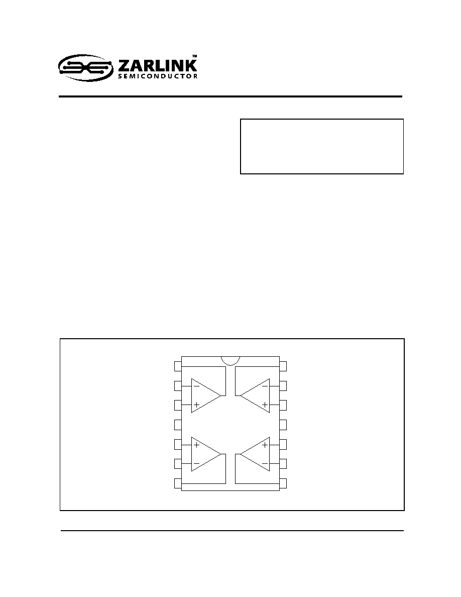
Figure 1 - Functional Block Diagram and Pin Connection
7
Out_1
In_n_1
In_p_1
In_p_2
In_n_2
Out_2
Out_4
In_n_4
In_p_4
V-
In_p_3
In_n_3
Out_3
ZL40122
V+
1
2
3
4
5
6
8
9
10
11
12
13
14
1
2
3
4

ZL40122
Data Sheet
2
Zarlink Semiconductor Inc.
Application Notes
Current Feedback Op Amps
Current feedback op amps offer several advantages over voltage feedback amplifiers:
∑ AC bandwidth not dependent on closed loop gain
∑ High Slew Rate
∑ Fast settling time
The architecture of the current feedback opamp consists of a high impedance non-inverting input and a low
impedance inverting input which is always feedback connected. The error current is amplified by a transimpedance
amplifier which can be considered to have gain
where Z
o
is the DC gain.
It can be shown that the closed loop non-inverting gain is given by
where Av is the DC closed loop gain, R
f
is the feedback resistor. The closed loop bandwidth is therefore given by
and for low values of closed loop gain Av depends only on the feedback resistor R
f
and not the closed loop gain.
Increasing the value of R
f
∑ Increases closed loop stability
∑ Decreases loop gain
∑ Decreases bandwidth
∑ Reduces gain peaking
∑ Reduces overshoot
Using a resistor value of R
f
=510
for Av=+2 V/V gives good stability and bandwidth. However since requirements
for stability and bandwidth vary it may be worth experimentation to find the optimal R
f
for a given application.
Layout Considerations
Correct high frequency operation requires a considered PCB layout as stray capacitances have a strong influence
over high frequency operation for this device. The Zarlink evaluation board serves as a good example layout that
should be copied. The following guidelines should be followed:
∑ Include 6.8uF tantalum and 0.1uF ceramic capacitors on both positive and negative supplies
∑ Remove the ground plane under and around the part, especially near the input and output pins to reduce
parasitic capacitances
∑ Minimize all trace lengths to reduce series inductance
+
=
o
o
f
f
j
Z
f
Z
1
)
(
+
=
o
o
f
Z
f
fR
j
Av
Vin
Vout
1
f
OL
f
o
o
CL
R
GB
R
Z
f
BW
=
=

Data Sheet
ZL40122
3
Zarlink Semiconductor Inc.
Application Diagrams
Figure 2 - Non-inverting Gain
Figure 3 - Inverting Gain
6.8uF
0.1uF
0.1uF
6.8uF
Vcc
Vin
Vout
Rin
Ra
Rf
Vee
º ZL40122
Ra
Rf
Av
Vin
Vout
+
=
=
1
∑
∑
∑
∑
∑
∑
∑
∑
∑
6.8uF
0.1uF
0.1uF
6.8uF
Vcc
Vin
Vout
Rin
Ra
Rf
Vee
º ZL40122
Rb
Ra
Rf
Av
Vin
Vout
-
=
=
∑
∑
∑
∑
∑
∑
∑
∑
∑

ZL40122
Data Sheet
4
Zarlink Semiconductor Inc.
Absolute Maximum Ratings
Note 1: Absolute Maximum Ratings indicate limits beyond which damage to the device may occur. Operating Ratings indicate
conditions for which the device is intended to be functional, but specific performance is not guaranteed. For guaranteed
specifications and the test conditions, see the Electrical Characteristics.
Note 2: Human body model, 1.5k
in series with 100pF. Machine model, 20in series with 100pF.
Note 3: 0.8kV between the pairs of +INA, -INA and +INB pins only. 2kV between supply pins, OUTA or OUTB pins and any input pin.
Note 4: ±100mA applied to input and output pins to force the device to go into "latch-up". The device passes this test to JEDEC spec
17.
Note 5: Positive and Negative supply transient testing increases the supplies by 20% for 100ms.
Operating Range
Parameter
Symbol
Min
Max
Units
1
Vin Differential
V
IN
±1.2
V
2
Output Short Circuit Protection
V
OS/C
See Apps
Note in this
data sheet
3
Supply voltage
V+, V-
±6.5
V
4
Voltage at Input Pins
V
(+IN)
, V
(-IN)
V-
V+
V
5
Voltage at Output Pins
V
O
V-
V+
V
6
EDS Protection
(HBM Human Body Model)
(see Note 2)
2
(see Note 3)
kV
7
Storage Temperature
-55
+150
∞C
8
Latch-up test
±100
mA
for 100ms
(see Note 4)
9
Supply transient test
20% pulse
for 100ms
(see Note 5)
Characteristic
Min
Typ
Max
Units
Comments
Supply Voltage (Vcc)
±4.0
±
6.0
V
Operating Temperature (Ambient)
-40
+85
∞C
Junction to Ambient resistance
Rth(j-a)
150
∞C
4 layer
FR4 board
Junction to Case resistance
Rth(j-c)
60
∞C
4 layer
FR4 board

Data Sheet
ZL40122
5
Zarlink Semiconductor Inc.
Electrical Characteristics
- Vcc=
±5V, T
amb
=25C(typ.),T
amb
=-40C to +85C(min-max), Av=+2V/V,
Rf=510
, Rload=100 unless specified.
Characteristic
Conditions
Typ
25C
Min/
Max
25C
Min/
Max
≠
40 to
+85C
Units
Test
Type
1
Frequency Domain Response
-3dB Bandwidth
Av=+1; Vo < 0.5Vp-p;
Rf=1.5k
450
-
-
MHz
C
Av=+2; Vo < 0.5Vp-p;
Rf=510
380
-
-
MHz
C
Av=+2; Vo < 5V p-p;
Rf=510
170
-
-
MHz
C
+/- 0.1dB Flatness
Av=+2; Vo < 0.5Vp-p;
Rf=510
120
-
-
MHz
C
Differential Gain (NTSC)
Rload=150
0.01
-
-
%
C
Differential Phase (NTSC)
Rload=150
0.015
-
-
deg.
C
Time Domain Response
Rise and Fall Time
Vout=0.5V Step
1
-
-
ns
C
Vout=5V Step
2.8
-
-
ns
C
Settling Time to 0.1%
Vout=2V Step
6
-
-
ns
C
Overshoot
Vout=0.5V Step
4
-
-
%
C
Slew Rate
Vout=5V Step
1500
-
-
V/
µs
C
Noise and Distortion
2
nd
Harmonic Distortion
Vout=2Vp-p, 1MHz
-84
-
-
dBc
C
3
nd
Harmonic Distortion
Vout=2Vp-p, 1MHz
-85
-
-
dBc
C
Equivalent Input Noise
Voltage
>1MHz
5.5
-
-
nV
C
Non-Inverting Current
>1MHz
1.3
-
-
pV
C
Inverting Current
>1MHz
11
-
-
pA
C
Static, DC Performance
Input Offset Voltage
2.7
±6.3
±7.7
mV
A
Average Drift
-
-
15
µV/deg. C
C
Input Bias Current ≠ Non-inverting
2.6
±5.6
±6
uA
A
Average Drift
-
-
6
nA/deg. C
C
Hz
Hz
Hz