Document Outline
- Features
- Applications
- Figure 2 - Pinout of 16 Pin SSO16 Package (Top View)
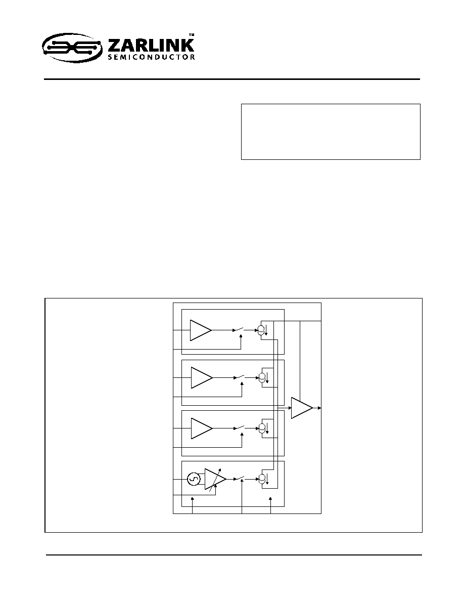
- Figure 1 - Functional Block Diagram
- Description
- Application Notes
- Read and Write Channel Operation
- On-Chip RF Oscillator
- Thermal Considerations
- Electrical and Optical Pulse Response
- Figure 3 - Pulse Response Model
- Specified Electrical Performance with 15�mm Interconnect and Zarlink ZLE40518 Evaluation Board
- Application Layer Guide Lines
- ZLE40518 Interconnect
- Figure 4 - ZLE40518 Application Board Electrical Interconnect
- Application Diagram
- Figure 5 - Evaluation Board Circuit
- Pin List
- Absolute Maximum Ratings
- Operating Range
- Package Thermal Resistance
- Electrical Characteristics - Vcc = 5�V, Tamb = 25∞C, PWR_UP = High, Ch2 and Ch3 disabled (/EN2 = ...
- Electrical Characteristics - Vcc = 5�V, Tamb = 25∞C, PWR_UP = High, unless otherwise specified.
- Electrical Characteristics: AC Performance - Vcc = 5�V, Iout = 40�mA DC with 40�mA pulse, Tamb = ...
- Characteristic Curves
- Figure 6 - Oscillator Frequency vs RF (RS=7.5�kW)
- Figure 7 - Oscillator Swing vs RS (RF=7.5�W)
- Figure 8 - Oscillator Frequency Dependency of Swing
- Figure 9 - Transfer Characteristic of Channel 2
- Figure 10 - Voltage Compliance R (IOUT to VCC) = 2.0�W
- Figure 11 - Step Response, Read Channel: 50�mA, Channel 2: 50mApp
- Figure 12 - Step Response, Read Channel: 50�mA, Channel 2: 250mApp
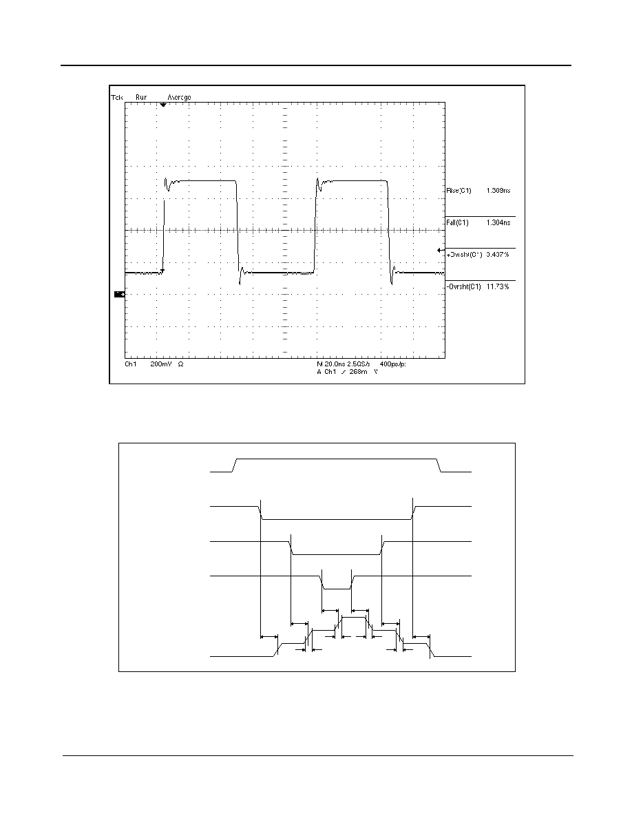
- Timing Waveforms
- Figure 13 - Output Waveform Showing Addition of Read and Write Levels
1
Zarlink Semiconductor Inc.
Zarlink, ZL and the Zarlink Semiconductor logo are trademarks of Zarlink Semiconductor Inc.
Copyright 2004-2005, Zarlink Semiconductor Inc. All Rights Reserved.
Features
∑ Current-controlled Output Current source
∑ Output Current per Channel to 250 mA
∑ Total Output Current to 300 mA
∑ Rise Time 1.0 ns, Fall Time 1.1 ns
∑ On-chip RF Oscillator
∑ External Resistor Control of Oscillator Swing and
Frequency
∑ 200 to 500 MHz Oscillator Range
∑ 100 mA Maximum Oscillator Swing
∑ Single +5 V Power Supply (±10%)
∑ Low-power Consumption
∑ Common Enable, Disable Input
∑ TTL/CMOS control signals
∑ Small SS016 Package
Applications
∑ DVD R/RW
∑ CD R/RW
February 2005
Ordering Information
ZL40518DGE1
16 Pin QSOP*
Tubes
*Pb Free Matte Tin
0
∞C to +70∞C
ZL40518
3 Channel Laser Diode Driver
Data Sheet
Figure 1 - Functional Block Diagram
IOUT
VCC
CH_2
CH_3
CH_R
RF_freq
RF_mag
INR
/ENR
IN2
/EN2
IN3
/EN3
RF
RS
GND
OSCEN
PWR_UP

ZL40518
Data Sheet
2
Zarlink Semiconductor Inc.
Figure 2 - Pinout of 16 Pin SSO16 Package (Top View)
Description
The ZL40518 is a laser diode driver for high speed operation of a grounded laser diode. The driver consists of 3
controllable channels: a switchable, low noise, read channel and two switchable write channels. Write current
pulses are enabled with the application of a low signal on the /EN pins. A summed output of all channels is
available at the IOUT pin. Each channel can contribute up to 250 mA to the total output current of up to 300 mA. A
total read channel gain of 100 and write channels 2 and 3 with a gain of 250 and 150 respectively are provided
between each reference current input and output.
Laser mode hopping noise during read mode can be reduced by the use of an on-chip RF oscillator. The oscillator
frequency and swing can be set by two external resistors. The oscillator is enabled by a high signal on the OSCEN
pin and the entire device can be switched off by the application of a low signal on the PWR_UP pin.
Application Notes
Read and Write Channel Operation
The read channel is activated by applying a 'High' signal to the PWR_UP pin and applying a 'low' signal to /ENR. In
this mode, the fast write channels can be enabled by applying a 'Low signal to the respective pair of write enable
pins (/EN2) or (/EN3). The output currents of the three channels are summed together and output as a composite
signal at IOUT.
Voltage control of the channel reference inputs (INR, IN2 and IN3) can be achieved quite easily using an external
resistor R
ref
in series with the reference channel input to convert a given reference potential V
ref
to an input current,
I
in
:
where R
in
is the input impedance of the respective reference channel.
On-Chip RF Oscillator
An on-chip RF oscillator is enabled if OSCEN = 'High', and its output signal is added to the current output.The
oscillator amplitude is set by an external resistor from RS to GND. Its frequency is set by an external resistor RF to
GND. The oscillator signal is summed with the programmed Write and Read levels before amplification to the
output. The oscillator signal has zero DC level and +I_pk to -I_pk signal swing. Consequently, if the programmed
DC level from the Write and Read Channels is less than the PK level programmed for the Oscillator, the combined
INR
IN2
GND
RF
IN3
/ENR
/EN2
/EN3
VCC_IN
VCC
IOUT
GND
RS
OSCEN
VCC
1
3
12
13
6
8
4
2
10
5
7
9
11
14
15
16
PWR_UP
in
ref
ref
in
R
R
V
I
+
=
,

ZL40518
Data Sheet
3
Zarlink Semiconductor Inc.
signal will be clipped on the negative cycle of the signal. This will increase the harmonic content of the output signal
and reduce the pk to pk amplitude output.
Thermal Considerations
Package thermal resistance is 40
∞ C/W under the EIA/JESD51-3 compliant PCB test board condition. Users should
ensure that the junction temperature does not exceed 150
∞C. Thermal resistance from junction to case and to
ambient is very much dependent on how the IC is mounted onto the board, on the PCB layout and on any heat
extraction arrangements. Power consumption and system ambient operating temperature limits should be noted
and careful thermal gradient calculations undertaken to ensure that the junction temperature never exceeds 150
∞C.
Electrical and Optical Pulse Response
Figure 3 - Pulse Response Model
Figure 3 illustrates a simplified model of the typical ZL40518 and the application. The ZL40518 consist of an ideal
switched current source and an equivalent model of the ZL40518 output stage. The Electrical Model for the Laser
Diode is a Voltage source Vd (V_on) in series with the On Resistance Rd all in parallel with the Junction
Capacitance Cd. This simplified model approximately represents the Laser Diode Electrical load when operated
beyond the Laser Threshold. To a first approximation, the Optical output is proportional to the current flow in the
Resistor Rd.
The Laser Diode and the ZL40518 are connected together by interconnect tracks with the return current passing
through the supply decoupling bypass capacitor between ground and output Vcc. The ZL40518 will typically switch
the programmed output current in 400 ps and can be approximated to an ideal switch with a propagation delay of
Iout_on (1.2 nS). The electrical pulse response parameters, Trise, Tfall, Overshoot and Undershoot are determined
by the combined electrical network as illustrated in Figure 3.
For example, the Rise Time and Fall time for large current steps can be slew rate limited by the combined
interconnect and fixed interconnect inductance. The Fixed Inductance represents that associated with packaging
and minimum interconnect distance . The Interconnect Inductance is that associated with the additional tracking
between Laser Diode and the ZL40518 to accommodate application physical limitations.
For example, if a pulse of 260 mA amplitude (40 mA to 300 mA) is to be switched in a time of 1 ns with the Vd =
1.6 V, then the maximum volt drop across the interconnect inductance is approximately 3.5 V (maximum Vpin for
300 mA output) - 1.6 V (Vdiode) = 1.9 V. Consequently, L*di/dt < 1.9 V. Hence , L < 1.9/ (0.26A/1ns)
= 7.3 nH.
En
Iout
500
17p
15
2p
ZL40518 Model
Vd
Rd
Cd
Lint
C_out
Lfix = 3nH
Lint=5nH , BW = 460MHz, Rd=7, Q=j20/(15+7) =0.9
Lint=5nH, BW = 460MHz, Rd=3, Q=j20/(15+3) = 1.11
Lint=7nH, BW = 411MHz, Rd=7, Q=j18/(15+7) = 0.8
Lint=7nH, BW = 411MHz,
Rd=3, Q=j18/(15+3) = 1.0
Lint
Lfix = 3nH
C_bypass
K
K
Vcc _A
OutA

ZL40518
Data Sheet
4
Zarlink Semiconductor Inc.
Small current step size Rise and Fall time will be determined by the Bandwidth of the combined network. This is
dominated by the Interconnect Inductance and the output Capacitance. Similarly, the overshoot and undershoot will
be determined by the Q of the network. This is a function of the Source Impedance from the ZL40518, the
Interconnect inductance and the Load impedance of the Laser Diode. Figure 3 includes example simplified
estimates of the Q and BW of the combined Laser Diode, ZL40518 and interconnect network for two different
interconnect inductance values (5 nH & 7 nH) and two different Diode On resistance (3 Ohm & 7 Ohm) . This
simple analysis illustrates the change in BW and Q of the network depending on these parameters. This in Turn
effects the Rise Time and Fall time and the Overshoot and Undershoot performance achieved in the application.
Specified Electrical Performance with 15 mm Interconnect and Zarlink ZLE40518 Evaluation Board
The specified performance in the table are results based on the electrical measurements and simulations across
full process corners using the Zarlink Evaluation Board using a 6.8 Ohm resistive load to ground. The track
interconnect between ZL40518 and the 6.8 Ohm Resistor is 15 mm long and uses a 2 mm wide track on single
sided FR4 board. The return path is via two 2 mm wide tracks spaced 0.25 mm either side of the track between
output and the 6.8 ohm resistor. The combined forward and return path forms a co planar transmission line with a
characteristic impedance of approximately 120 ohms. The tight coupled return paths carrying the return current
reduce the effective series inductance (Leff) which can be approximated to:-
L
eff
= 2 * Lint * (1 - K) + 2 * Lfix * (1 - K).
The ZLE40518 board has two positions for the Laser Diode at two different distances. (15 and 30 mm).
The measured value of L
eff
is 7 nH.
The estimated value of L
eff
= 2 * 8 (1 - 0.5) = 8 nH.
The actual pulse response achieved in an application is thus dependent on the application.
Application Layer Guide Lines
Minimize Interconnect Inductance by:-
a. Using Short Interconnect Distance
b. Use wide interconnect tracks
c. Keep the return path tightly coupled to the forward path

ZL40518
Data Sheet
5
Zarlink Semiconductor Inc.
ZLE40518 Interconnect
Figure 4 - ZLE40518 Application Board Electrical Interconnect
Application Diagram
Figure 5 - Evaluation Board Circuit
INR
IN2
GND
RF
IN3
/ENR
/EN2
/EN3
VCC
IOUT
GND
RS
PWR_UP
OSCEN
VCC
1
3
12
13
4
8
4
2
10
5
7
9
11
14
15
16
DIGITAL
INPUTS
ANALOG
INPUTS
VCC
LASER
DIODE
VCC_IN

ZL40518
Data Sheet
6
Zarlink Semiconductor Inc.
Pin List
Pin No.
Pin name
Type
Function
1
INR
Analog
Read Channel Input Current
2
IN2
Analog
Channel 2 Input Current
3
GND
Supply
Ground
4
RF
Analog
External Resistor to ground to set Oscillator Frequency
5
IN3
Analog
Channel 3 Input Current
6
/ENR
Digital
Digital control of Read Channel (active low)
7
/EN2
Digital
Digital control of Channel 2 (active low)
8
/EN3
Digital
Digital control of Channel 3 (active low)
9
VCC
Supply
+5 V supply
10
OSCEN
Digital
Enables RF oscillator (active high)
11
PWR_UP
Digital
Device Power Up (active high)
12
RS
Analog
External Resistor to ground to set Oscillator Amplitude
13
GND
Supply
Ground
14
IOUT
Analog
Output current for laser diode
15
VCC
Supply
+5 V supply
16
VCC_IN
Supply
+5 V supply

ZL40518
Data Sheet
7
Zarlink Semiconductor Inc.
Absolute Maximum Ratings
Permanent damage may occur to any device stressed beyond the "Absolute Maximum Ratings". Operation at or beyond this stress rating is not
implied for this or following sections of this specification. Device reliability can be affected by prolonged exposure to absolute maximum ratings.
Note 1: R
thJA
115∞C/W, T
amb
= 70 C
Note 2: R
thJA
115∞C/W, T
amb
= 25∞C
Operating Range
Package Thermal Resistance
Note 1: Measured with a multilayer test board (JEDEC standard).
Parameters
Symbol
Value
Unit
Supply voltage
V
cc
-0.5 to +6.0
V
Input voltage at INR, IN2, IN3
V
IN1
-0.5 to +2.0
V
Input voltage at PWR_UP, /ENR, /EN2,
/EN3, OSCEN
V
IN2
-0.5 to V
cc
+ 0.5
V
Output voltage
V
OUT
-0.5 to V
cc
- 1
V
Power dissipation
P
Max
0.7
1
to 1
2
W
Junction temperature
T
J
150
C
Storage temperature range
T
Stg
-65 to +125
C
Characteristic
Symbol
Units
Unit
Supply voltage range
V
cc
4.5 to 5.5
V
Input current
I
INR
I
IN2
I
IN3
<2.5
<1.0
<1.7
mA
External resistor to GND to set oscillator
frequency
RF
>3
k
External resistor to GND to set oscillator
swing
RS
>2
k
Operating temperature range
T
amb
0 to +70
C
Parameters
Symbol
Value
Unit
Junction ambient
R
thJA
115
1
K/W

ZL40518
Data Sheet
8
Zarlink Semiconductor Inc.
Electrical Characteristics -
Vcc = 5 V, T
amb
= 25
∞
C, PWR_UP = High, Ch2 and Ch3 disabled (/EN2 = /EN3 = high), Read enabled
(/ENR = low), OSCEN = Low, unless otherwise specified.
* A = 100% tested, B = 100% correlation tested, C = Characterized on samples, D = Design parameter
Parameters
Test
Conditions
Pin.
Symbol
Min.
Typ.
Max.
Unit
Type*
Power Supply
Supply current, power
down
PWR_UP =
Low, /EN2 =
/EN3 = Low
9, 15,
16
ICC
PD2
0.4
mA
A
Supply current, read
mode, oscillator disabled
I
INR
=500
µA,
I
IN2
= 200
µA,
I
IN3
= 333
µA
9, 15,
16
ICC
R1
86
mA
A
Supply current, read
mode, oscillator enabled
I
INR
=500
µA,
I
IN2
= 200
µA,
I
IN3
= 333
µA,
OSCEN = High,
RS = 7.5 k
,
RF = 7.5 k
9, 15,
16
ICC
R2
90
mA
A
Supply current, write
mode
I
INR
=500
µA,
I
IN2
= 200
µA,
I
IN3
= 333
µA,
/EN2 = /EN3 =
Low
9, 15,
16
ICC
W
180
mA
A
Supply current, input off
I
INR
= I
IN2
= I
IN3
= 0
µA
9, 15,
16
ICC
off
15
mA
A
Digital Inputs
/ENR, /EN2, /EN3 low
voltage
6, 7, 8
VNE
LO
1.2
V
A
/ENR, /EN2, /EN3 high
voltage
6, 7, 8
VNE
HI
1.9
V
A
PWR_UP Low Voltage
11
VEN
LO
0.5
V
A
PWR_UP High Voltage
11
VEN
HI
2.7
V
A
OSCEN low voltage
10
VEO
LO
0.5
V
A
OSCEN high voltage
10
VEO
HI
3.0
V
A
Current at Digital Inputs
/ENR, /EN2, /EN3 low
current
/EN = 0 V
6, 7, 8
INE
LO
-300
µA
C
/ENR, /EN2, /EN3 high
current
/EN = 5 V
6, 7, 8
INE
HI
800
µA
C
PWR_UP Low Current
PWR_UP = 0 V
11
IEN
LO
-150
µA
C
PWR_UP High Current
PWR_UP = 5 V
11
IEN
HI
100
µA
C
OSCEN low current
OSCEN = 0 V
10
IEO
LO
-100
µA
C
OSCEN high current
OSCEN = 5 V
10
IEO
HI
800
µA
C

ZL40518
Data Sheet
9
Zarlink Semiconductor Inc.
Electrical Characteristics
- Vcc = 5 V, Tamb = 25
∞
C, PWR_UP = High, unless otherwise specified.
*A = 100% tested, B = 100% correlation tested, C = Characterized on samples, D = Design parameter
Note 1: Linearity of the amplifier is calculated using a best fit method at three operating points of I
OUT
at 20 mA, 40 mA, and 60 mA.
I
OUT
= (I
IN
x GAIN) + I
OS
Parameters
Test Conditions
Pin
Symbol
Min.
Typ.
Max.
Unit
Type*
Output IOUT
Total output current
Output is sourcing
14
I
OUT
350
mA
A
Output current per
channel
Output is sourcing
14
I
OUTR
250
mA
A
I
OUT
series resistance
Total R
OUT
to V
CC
rail
14
R
OUT
2
C
Best fit current gain
INR
Channel R
1
14
GAINR
90
100
130
mA/
mA
A
Best fit current gain
IN2
Channel 2
1
14
GAIN2
225
250
325
mA/
mA
A
Best fit current gain
IN3
Channel 3
1
14
GAIN3
135
150
195
mA/
mA
A
Best fit current offset
Any channel
1
14
IOS
2.6
mA
A
Output current linearity
Any channel
1
14
ILIN
-3
+3
%
A
I
IN
input impedance
R
IN,INR
is to GND
1
R
IN,INR
500
C
I
IN
input impedance
R
IN,IN2
is to GND
2
R
IN,IN2
1250
C
I
IN
input impedance
R
IN,IN3
is to GND
5
R
IN,IN3
750
C
EN threshold
Temperature
stabilised
6, 7, 8
VTH
1.6
V
C
Output off current 1
PWR_UP = Low
14
IOFF
1
1
mA
C
Output off current 2
/EN2 = /EN3 = High,
I
INR
= 0,
I
IN2
= 200
µA,
I
IN3
= 333
µA
14
IOFF
2
1
mA
C
Output off current 3
/EN2 = /EN3 = Low,
I
INR
= I
IN2
= I
IN3
=
0
µA
14
IOFF
3
5
mA
C
I
OUT
supply sensitivity,
write mode
IOUT = 80 mA,
40 mA read + 40 mA
write, VCC = 5 V +/-
10%
14
VSE
W
6
%/V
C
I
OUT
current output
noise
IOUT = 40 mA,
OSCEN = Low
14
INO
O
3
nA/rt-
Hz
C

ZL40518
Data Sheet
10
Zarlink Semiconductor Inc.
Electrical Characteristics: AC Performance
- Vcc = 5 V, Iout = 40 mA DC with 40 mA pulse, Tamb = 25
∞C, unless otherwise
specified.
*
A = 100% tested, B = 100% correlation tested, C = Characterized on samples, D = Design parameter
Note 1: Load resistor at I
OUT
6.8 ohms, measurement with 50 ohm oscilloscope and 39 ohm series resistor.
Parameters
Test Conditions
Pin.
Symbol
Min.
Typ.
Max.
Unit
Type*
Output AC Performance
Write rise time
I
OUT
= 40 mA (read) +
40 mA (10 to 90%)
1
14
t
RISE
1.0
ns
C
Write fall time
I
OUT
= 40 mA (read) +
40 mA (10 to 90%)
1
14
t
FALL
1.1
ns
C
Output current
overshoot
I
OUT
= 40 mA (read) +
40 mA
1
14
OS
5
%
C
I
OUT
ON propagation
delay
/EN 50% High-Low to
I
OUT
at 50% of final value
14
t
ON
2.2
ns
C
I
OUT
OFF propagation
delay
/EN 50% Low-High to
I
OUT
at 50% of final value
14
t
OFF
2.0
ns
C
Disable time
PWR_UP 50% High-Low
to Iout at 50% of final
value
14
t
DIS
20
ns
C
Enable time
PWR_UP 50% Low-High
to Iout at 50% of final
value
14
t
EN
23
ns
C
Amplifier bandwidth
I
OUT
= 50 mA, all
channels, -3 dB value
14
BW
LCA
28
MHz
C
Oscillator
Oscillator frequency
RF = 7.5 k
14
F
OSC
288
322
352
MHz
A
Osc. Temperature
coefficient
RF = 7.5 k
14
TC
OSC
+150
ppm/
C
C
Disable time oscillator
OSCEN 50% High-Low to
I
OUT
at 50% of final value
14
T
DISO
4
ns
C
Enable time oscillator
OSCEN 50% Low-High to
I
OUT
at 50% of final value
14
T
ENO
2
ns
C

ZL40518
Data Sheet
11
Zarlink Semiconductor Inc.
Characteristic Curves
Figure 6 - Oscillator Frequency vs RF (RS=7.5 k
)
Vcc = 5 V, Temp = 25
∞C
Figure 7 - Oscillator Swing vs RS (RF=7.5
)
Vcc = 5 V, Temp = 25
∞C
2 0 0
3 0 0
4 0 0
5 0 0
6 0 0
7 0 0
8 0 0
2 .0 0
3 .0 0
4 .0 0
5 .0 0
6 .0 0
7 .0 0
8 .0 0
9 .0 0
1 0 .0 0
1 1 .0 0
1 2 .0 0
R F (k O h m )
Frequency (MHz)
0
20
40
60
80
100
120
2
3
4
5
6
7
8
9
10
RS (kOhm s)
Amplitude (mApk-pk)

ZL40518
Data Sheet
12
Zarlink Semiconductor Inc.
Figure 8 - Oscillator Frequency Dependency of Swing
Vcc = 5 V, Temp = 25
∞C
Figure 9 - Transfer Characteristic of Channel 2
(Gain = 278, Load Resistor at IOUT = 6.8
)
0
10
20
30
40
50
60
200
250
300
350
400
450
500
Frequency (MHz)
Amplitude (mApk-pk
)
0
100
200
300
400
500
0
200
400
600
800
1000
1200
1400
1600
1800
2000
Input Current (uA)
Iout (mA)

ZL40518
Data Sheet
13
Zarlink Semiconductor Inc.
Figure 10 - Voltage Compliance R (IOUT to VCC) = 2.0
Figure 11 - Step Response, Read Channel: 50 mA, Channel 2: 50mApp
0
0 . 0 5
0 . 1
0 . 1 5
0 . 2
0 . 2 5
0 . 3
0 . 3 5
0 . 4
0
1
2
3
4
5
6
V o u t (V )
Iout (A)
ZL40518
Data Sheet
14
Zarlink Semiconductor Inc.
Figure 12 - Step Response, Read Channel: 50 mA, Channel 2: 250mApp
Timing Waveforms
Figure 13 - Output Waveform Showing Addition of Read and Write Levels
t
PWR_UP
/ENR
/EN2
/EN3
EN
t
ON
t
ON
t
OFF
t
OFF
t
DIS
t
R
t
R
t
R
t
R


www.zarlink.com
Information relating to products and services furnished herein by Zarlink Semiconductor Inc. or its subsidiaries (collectively "Zarlink") is believed to be reliable.
However, Zarlink assumes no liability for errors that may appear in this publication, or for liability otherwise arising from the application or use of any such
information, product or service or for any infringement of patents or other intellectual property rights owned by third parties which may result from such application or
use. Neither the supply of such information or purchase of product or service conveys any license, either express or implied, under patents or other intellectual
property rights owned by Zarlink or licensed from third parties by Zarlink, whatsoever. Purchasers of products are also hereby notified that the use of product in
certain ways or in combination with Zarlink, or non-Zarlink furnished goods or services may infringe patents or other intellectual property rights owned by Zarlink.
This publication is issued to provide information only and (unless agreed by Zarlink in writing) may not be used, applied or reproduced for any purpose nor form part
of any order or contract nor to be regarded as a representation relating to the products or services concerned. The products, their specifications, services and other
information appearing in this publication are subject to change by Zarlink without notice. No warranty or guarantee express or implied is made regarding the
capability, performance or suitability of any product or service. Information concerning possible methods of use is provided as a guide only and does not constitute
any guarantee that such methods of use will be satisfactory in a specific piece of equipment. It is the user's responsibility to fully determine the performance and
suitability of any equipment using such information and to ensure that any publication or data used is up to date and has not been superseded. Manufacturing does
not necessarily include testing of all functions or parameters. These products are not suitable for use in any medical products whose failure to perform may result in
significant injury or death to the user. All products and materials are sold and services provided subject to Zarlink's conditions of sale which are available on request.
Purchase of Zarlink's I
2
C components conveys a licence under the Philips I
2
C Patent rights to use these components in and I
2
C System, provided that the system
conforms to the I
2
C Standard Specification as defined by Philips.
Zarlink, ZL and the Zarlink Semiconductor logo are trademarks of Zarlink Semiconductor Inc.
Copyright Zarlink Semiconductor Inc. All Rights Reserved.
TECHNICAL DOCUMENTATION - NOT FOR RESALE
For more information about all Zarlink products
visit our Web Site at