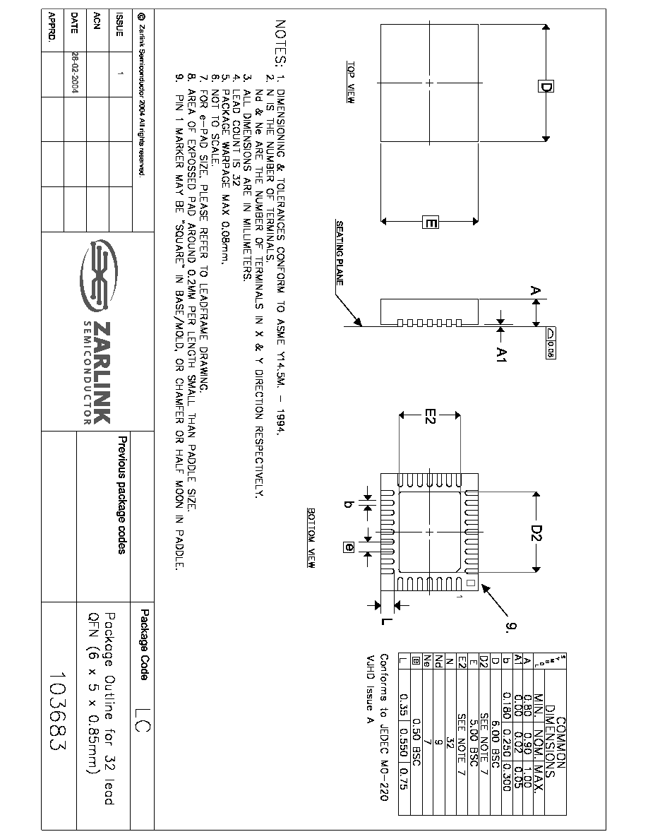
Document Outline
- Features
- Applications
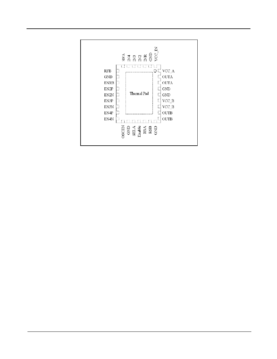
- Figure 2 - Pinout for 5 x 6�mm 32 pin QFN (top view)
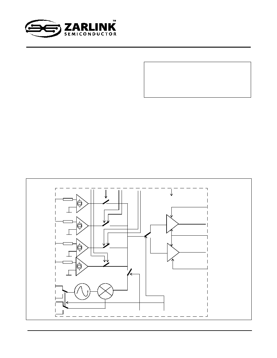
- Figure 1 - ZL40539 Block Diagram
- Description
- Application Notes
- Read and Write Channel Operation
- On-chip RF Oscillator
- Thermal Considerations
- Electrical and Optical Pulse Response
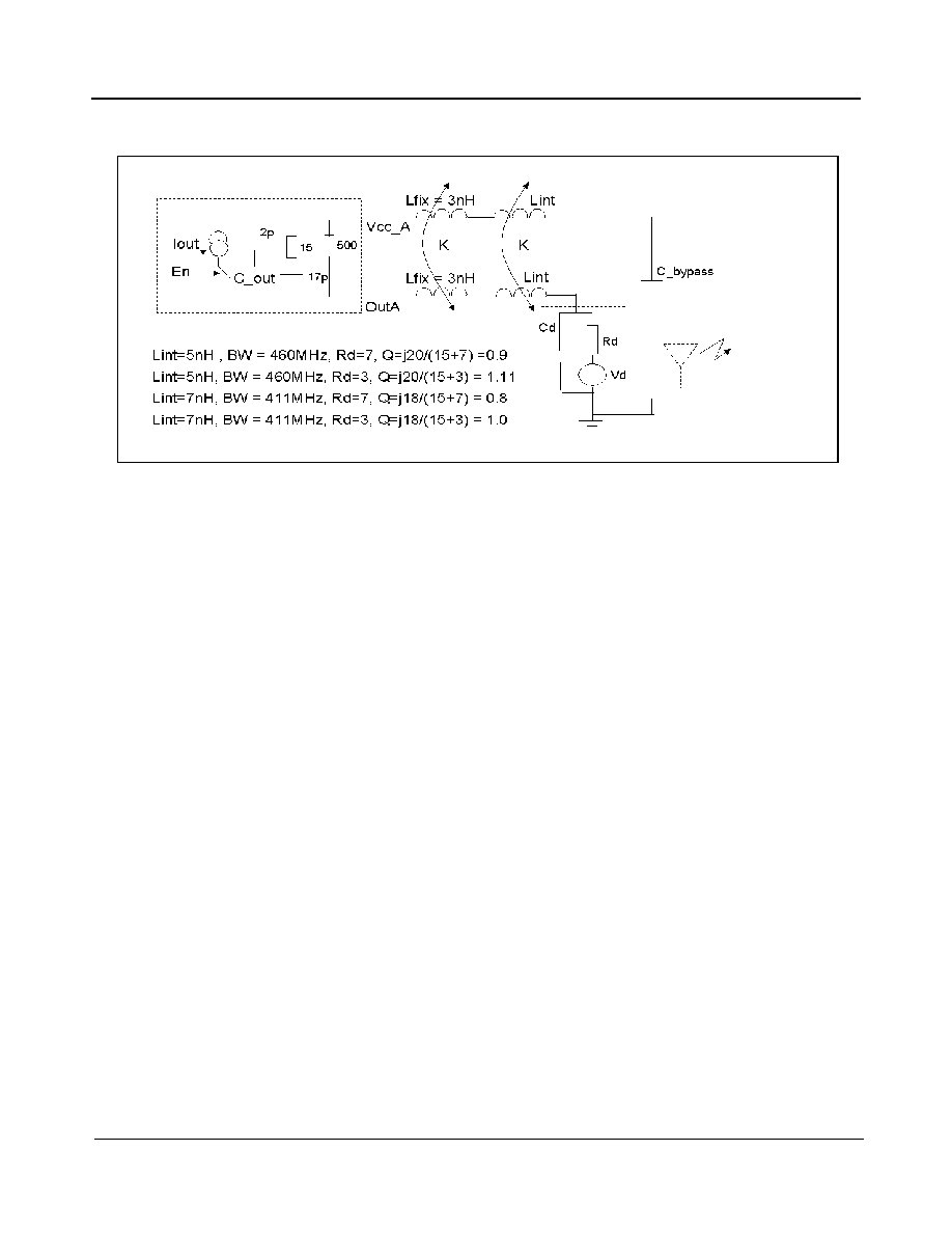
- Figure 3 - Pulse Response Model
- Specified Electrical Performance with 15 mm Interconnect and Zarlink ZLE40539 Evaluation Board
- ZL40539E Interconnect
- Figure 4 - ZLE40539 Application Board Electrical Interconnect
- Application Diagram
- Figure 5 - Application Schematic Diagram
- Evaluation Boards From Zarlink Semiconductor
- Pin List
- Absolute Maximum Ratings
- Operating Range
- Package Thermal Resistance
- Electrical Characteristics - Supply Current and Digital Inputs - Vcc = 5�V, Tamb = 25�C, INR = IN...
- Electrical Characteristics - Outputs A and B - Vcc = 5�V, Tamb = 25�C, Enable = High, ChR, Ch2, C...
- Electrical Characteristics - Timing - Vcc = 5�V, Tamb = 25�C, Enable = High, Ch2, Ch3, Ch4 disabl...
- Min.
- Typ.
- Max.
- Electrical Characteristics - Oscillator - Vcc = 5�V, Tamb = 25�C, INR = 400�uA, IN2 = IN3 = IN4 =...
- Characteristic Curves
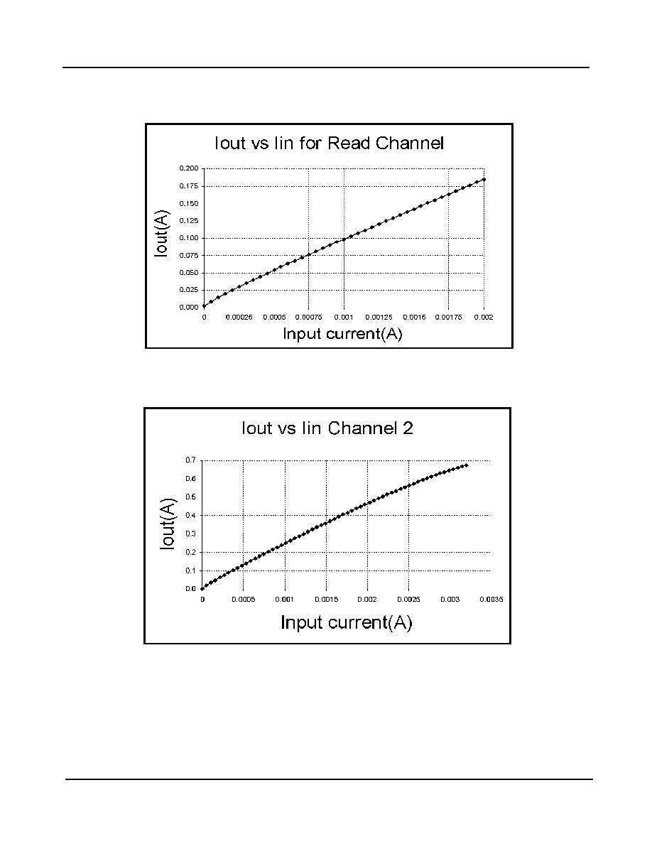
- Figure 6 - Iout vs Iin for Read Channel
- Figure 7 - Iout vs Iin Channel 2
- Figure 8 - Iout vs Iin Channel 3
- Figure 9 - Iout vs Iin Channel 4
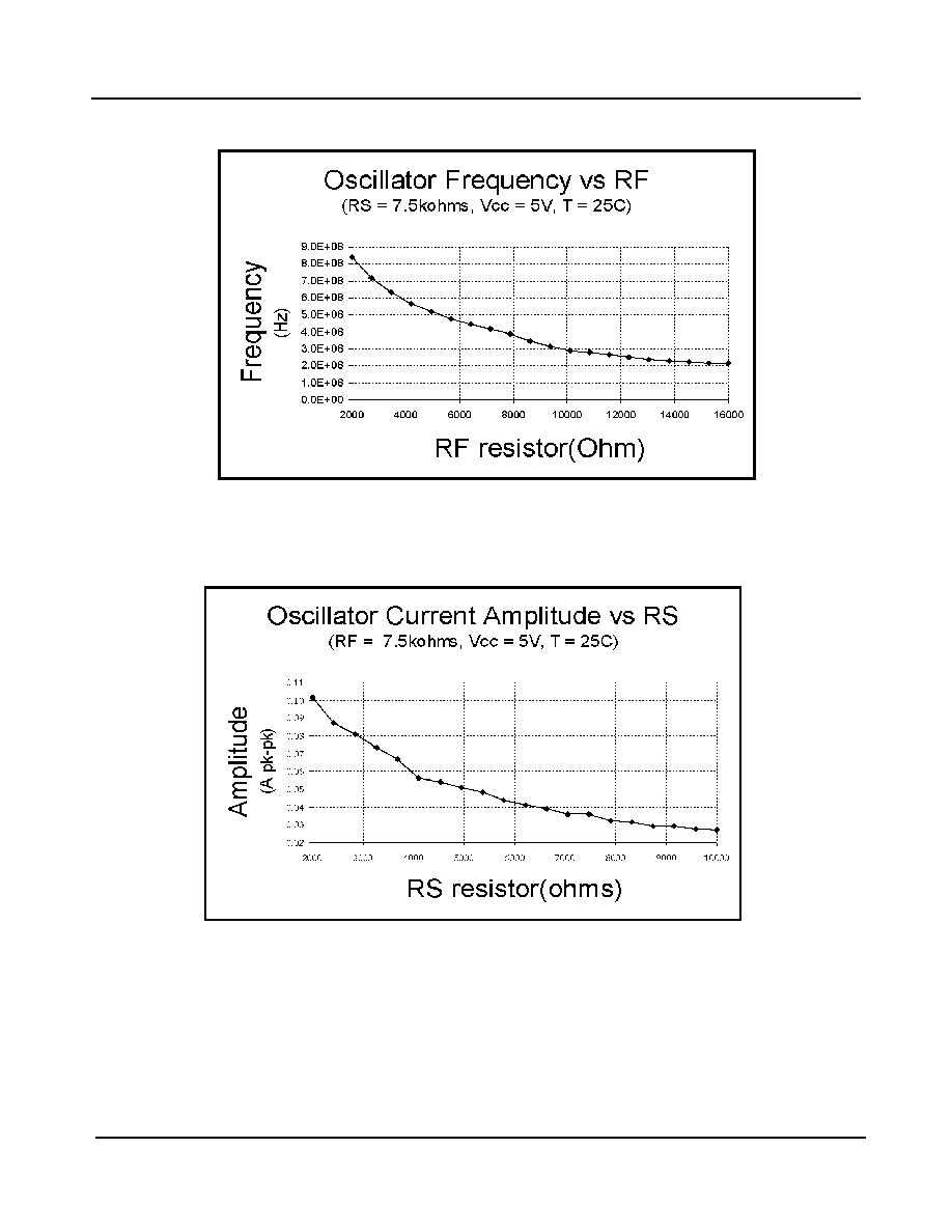
- Figure 10 - Oscillator Frequency vs RF
- Figure 11 - Oscillator Current Amplitude vs RS
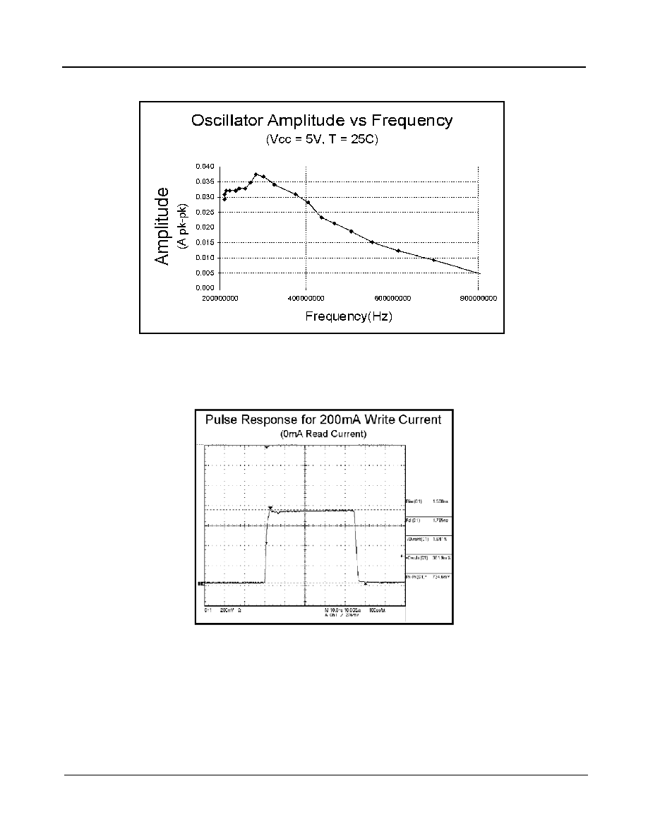
- Figure 12 - Oscillator Amplitude vs Frequency
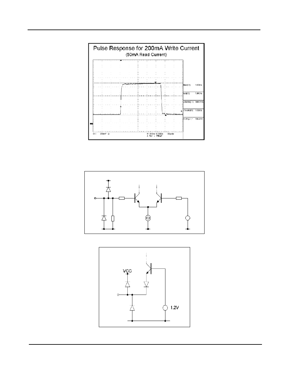
- Figure 13 - Pulse Response for 200�mA Write Current
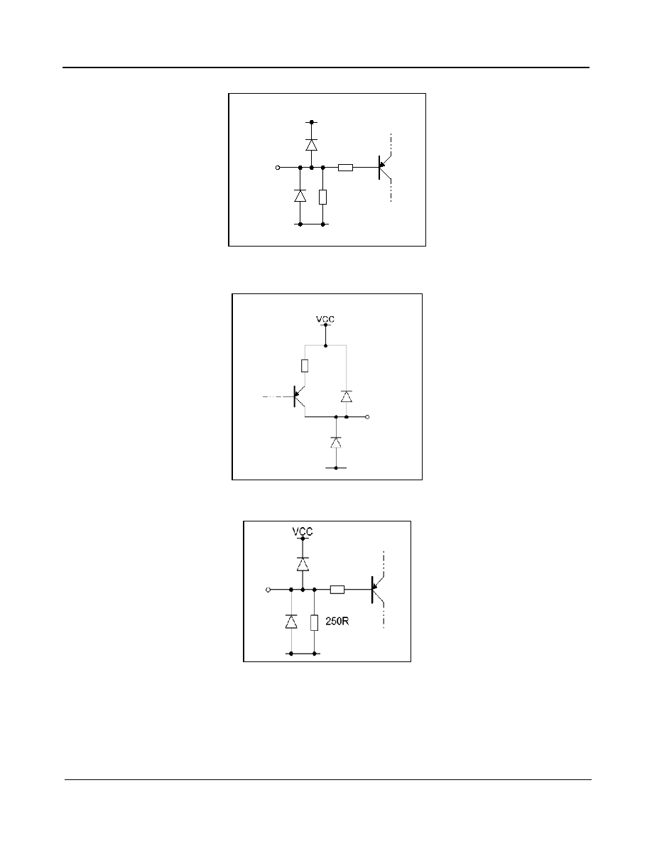
- Figure 14 - Pulse Response for 200�mA Write Current
- I/O diagrams
- Figure 15 - CMOS/LVTTL Input (Enable, OSCEN)
- Figure 16 - Oscillator Resistors (RF, RS)
- Figure 17 - Read Current Input (INR)
- Figure 18 - Output (OUTA, OUTB)
- Figure 19 - Write Current Input (IN2, IN3, IN4)
- Figure 20 - LVDS Input (EN2, /EN2), (EN3, /EN3), (EN4, /EN4)
- OUTA and OUTB Control
- Table 1 - Output Function for Set Logic Inputs
- Oscillator Control
- Table 2 - Output Function for Set Logic Inputs
- Timing Diagrams
- Figure 21 - Timing of Read or Write Channels
- Figure 22 - Timing of Output with Enable, Read and Write Levels
- Write Waveform
- Figure 23 - Write Waveform Example
- Oscillator Waveform
- Figure 24 - Example of the Oscillator Waveform Superimposed on the Read Waveform
1
Zarlink Semiconductor Inc.
Zarlink, ZL and the Zarlink Semiconductor logo are trademarks of Zarlink Semiconductor Inc.
Copyright 2004-2005, Zarlink Semiconductor Inc. All Rights Reserved.
Features
� Pin compatible with EL6839
� Dual output for CD/DVD laser
� LVDS control signal, internal 100 ohms
� Rise time 1.0 ns, Fall time 1.1 ns typical
� Low noise read channel with gain of 100x to
150 mA
� Channel 2 gain of 250x to 550 mA
� Channel 3 gain of 150x to 500 mA
� Channel 4 gain of 100x to 450 mA
� Combined total output current 700 mA
� On-chip oscillator with frequency and amplitude
control by external resistors
� Oscillator frequency to 575 MHz, amplitude to
100 mA pk to pk
� Power Up/Down control
� > 2 kV ESD Single 5 V supply (�10%)
� 32-pin QFN package
Applications
� DVD
�RW/RAM
� DVD
�R
� CD-RW
� CD-R
� Write optical drives
� Laser Diode current switch
� Supports double density DVD
February 2005
ZL40539
Dual Output CD and DVD
4 Channel Laser Diode Driver
Data Sheet
Figure 1 - ZL40539 Block Diagram
OSCEN
SELA
Chip Enable/Power
Enable
EN4
P/N ENRB
P/N
EN2
P/N
EN3
INR
IN2
IN3
IN4
VCC_A
OUTA
GND
OUTB
VCC_B
RFA
RFB
RSA
RSB
Ordering Information
ZL40539LCG Trays/Bake/Dry Pack
ZL40539LCF Tape/Reel Bake/Dry Pack
0
�C to +70�C
ZL40539
Data Sheet
2
Zarlink Semiconductor Inc.
Figure 2 - Pinout for 5 x 6 mm 32 pin QFN (top view)
Description
The ZL40539 is a high performance laser diode driver capable of driving two separate cathode grounded laser
diodes (e.g., 650 nm and 780 nm laser diodes).
The ZL40539 contains a 150 mA low noise read channel (ChR), and three >450 mA write channels (Ch2, Ch3 and
Ch4). Each channel amplifies the positive current supplied at its reference input (INR, IN2, IN3, IN4) by a fixed
factor of 100, 250, 150 and 100 respectively.
The device is enabled with a High level applied to the Enable Pin. The read channel is activated by applying a 'Low'
signal to the ENRB pin. Each fast write channel can be enabled by applying a positive voltage difference between
the enable pins (EN2P, EN2N), (EN3P, EN3N) and (EN4P, EN4N). The output currents of the four channels are
summed together and output as a composite signal at either OUTA (if SELA select is 'High') or OUTB (if SELA
select is 'Low'). This provides the ability to drive two different laser diodes with just one ZL40539.
Voltage control of the channel reference inputs (INR, IN2, IN3 and IN4) can be achieved by using an external
resistor in series with the reference channel input to convert a given reference potential to an input current.
An on-chip RF oscillator is provided for the reduction of laser mode hopping noise. The oscillator is enabled if
OSCEN = 'High', and its output signal is added to the appropriate current output (OUTA, if SELA select is 'High', or
OUTB, if SELA select is 'Low'). The oscillator amplitude is set by external resistors from RSA or RSB to GND. Its
frequency is set by an external resistor RFA or RFB to GND. RFA and RSA are selected when SELA = `High' and
RFB and RSB when SELA = 'Low'

ZL40539
Data Sheet
3
Zarlink Semiconductor Inc.
Application Notes
Read and Write Channel Operation
The device is activated by applying a 'High' signal to the Enable pin. In this mode, the read channel can be enabled
with a low signal on ENRB. The fast write channels can be enabled by applying a 'High' signal to the respective pair
of write enable pins (EN2P, EN2N), (EN3P, EN3N), or (EN4P, EN4N). The output currents of the four channels are
summed together and output as a composite signal at either OUTA (if SELA select is 'High') or OUTB (if SELA
select is 'Low'). This provides the ability to drive two different laser diodes with just one ZL40539.
Voltage control of the channel reference inputs (INR, IN2, IN3 and IN4) can be achieved quite easily using an
external resistor R
ref
in series with the reference channel input to convert a given reference potential V
ref
to an input
current, I
in
:
,
where R
in
is the input impedance of the respective reference channel.
On-chip RF Oscillator
An on-chip RF oscillator is enabled if OSCEN = 'High', and its output signal is added to the appropriate current
output (OUTA, if SELA select is 'High', or OUTB, if SELA select is 'Low'). The oscillator amplitude is set by an
external resistor from RSA or RSB to GND. Its frequency is set by an external resistor RFA or RFB to GND. RSA
and RFA are selected when SELA is `High'
The oscillator signal is summed with the programmed Write and Read levels before amplification to the output. The
oscillator signal has zero DC level and +I_pk to �I_pk signal swing. Consequently, if the programmed DC level from
the Write and Read Channels is less than the PK level programmed for the Oscillator, the combined signal will be
clipped on the negative cycle of the signal. This will increase the harmonic content of the output signal and reduce
the pk to pk amplitude output.
Thermal Considerations
Package thermal resistance is 40
�C/W under the EIA/JESD51-3 compliant PCB test board condition.
Users should ensure that the junction temperature does not exceed 150
�C. Thermal resistance from junction to
case and to ambient is very much dependent on how the IC is mounted onto the board, on the PCB layout and on
any heat extraction arrangements.
Power consumption and system ambient operating temperature limits should be noted and careful thermal gradient
calculations undertaken to ensure that the junction temperature never exceeds 150
�C.
in
ref
ref
in
R
R
V
I
+
=
ZL40539
Data Sheet
4
Zarlink Semiconductor Inc.
Electrical and Optical Pulse Response
Figure 3 - Pulse Response Model
Figure 3 illustrates a simplified model of the ZL40539 output and the application. The ZL40539 consists of an ideal
switched current source and an equivalent model of the ZL40539 output stage. The Electrical Model for the Laser
Diode is a Voltage source Vd (V_on) in series with the On Resistance Rd all in parallel with the Junction
Capacitance Cd. This simplified model approximately represents the Laser Diode Electrical load when operated
beyond the Laser Threshold. To a first approximation, the Optical output is proportional to the current flow in the
Resistor Rd.
The Laser Diode and the ZL40539 are connected together buy interconnect tracks with the return current passing
through the supply decoupling bypass capacitor between ground and output Vcc.
The ZL40539 will typically switch the programmed output current in 400 ps and can be approximated to an ideal
switch with a propagation delay of Iout_on (1.2 nS). The electrical pulse response parameters, Trise, Tfall,
Overshoot and Undershoot are determined by the combined electrical network as illustrated in Figure 3.
For example, the Rise Time and Fall time for large current steps can be slew rate limited by the combined
interconnect and fixed interconnect inductance. The Fixed Inductance represents that associated with packaging
and minimum interconnect distance. The Interconnect Inductance is that associated with the additional tracking
between Laser Diode and the ZL40539 to accommodate application physical limitations. For example:-
if a pulse of 360 mA amplitude (40 mA to 400 mA) is to be switched in a time of 1 nS with the Vd =
1.6 V, then:-
the maximum volt drop across the interconnect inductance is approximately 3.5 V (maximum Vpin
for 500 mA output) � 1.6 V (Vdiode) = 1.9 V.
Consequently, L*di/dt < 1.9 V.
Hence, L < 1.9/ (0.36A/1nS) = 5.3 nH.
Small current step size Rise and Fall time will be determined by the Bandwidth of the combined network. This is
dominated by the Interconnect Inductance and the output Capacitance. Similarly, the overshoot and undershoot will
be determined by the Q of the network. This is a function of the Source Impedance from the ZL40539, the
Interconnect inductance and the Load impedance of the Laser Diode. Figure 3 includes example simplified
estimates of the Q and BW of the combined Laser Diode, ZL40539 and interconnect network for two different
interconnect inductance values (5 nH & 7 nH) and two different Diode On resistance (3 Ohm & 7 Ohm). This simple
analysis illustrates the change in BW and Q of the network depending on these parameters. This in turn effects the
Rise Time and Fall time and the Overshoot and Undershoot performance achieved in the application.
ZL40539 Model

ZL40539
Data Sheet
5
Zarlink Semiconductor Inc.
Specified Electrical Performance with 15 mm Interconnect and Zarlink ZLE40539 Evaluation Board
The specified transient pulse performance in the table are results based on the electrical measurements and
simulations across full process corners using the Zarlink Evaluation Board using a 3.9 Ohm resistive load to
ground.
The track interconnect between ZL40539 and the 3.9 Ohm Resistor is 15 mm long and uses a 2 mm wide track on
single sided FR4 board. The return path is via two 2 mm wide tracks spaced 0.25 mm either side of the track
between output and the 3.9 ohm resistor. The combined forward and return path forms a co planar transmission
line with a characteristic impedance of approximately 120 ohms.
The tight coupled return paths carrying the return current reduce the effective series inductance (Leff) which can be
approximated to:-
Leff = 2 * Lint * (1 - K) + 2 * Lfix * (1 - K).
The ZLE40539 board has two positions for the Laser Diode at two different distances. (15 and 30 mm).
The measured value of Leff is 7 nH.
The estimated value of Leff = 2 * 8 (1 � 0.5) = 8 nH.
The actual pulse response achieved in an application is thus dependent on the application.
Application Layout Guide Lines
Minimize Interconnect Inductance by:
1. Using Short Interconnect Distance
2. Use wide interconnect tracks
3. Keep the return path tightly coupled to the forward path
ZL40539E Interconnect
Figure 4 - ZLE40539 Application Board Electrical Interconnect

ZL40539
Data Sheet
6
Zarlink Semiconductor Inc.
Application Diagram
Figure 5 - Application Schematic Diagram
Evaluation Boards From Zarlink Semiconductor
Zarlink Semiconductor provide an LDD evaluation board. This is primarily for those interested in performing their
own assessment of the operation of the LDD. Figure 5 shows a recommended application configuration. The inputs
are connected via side launch SMA connectors.
Please order as ZLE40539.
ZL40539
Data Sheet
7
Zarlink Semiconductor Inc.
Pin List
Pin
Pin Name
Type
Function
1
VCC_IN
Supply
Input Vcc
2
GND
Supply
Ground
3
INR
Analog
Current input, R
in
= 500
to GND
4
IN2
Analog
Current input, R
in
= 500
to GND
5
IN3
Analog
Current input, R
in
= 500
to GND
6
IN4
Analog
Current input, R
in
= 500
to GND
7
RFA
Analog
Resistor to GND sets oscillator frequency when SELA='High'
8
RFB
Analog
Resistor to GND sets oscillator frequency when SELA='Low'
9
GND
Supply
Ground
10
ENRB
Digital, CMOS
Enable Read Bar for Read Channel
11
EN2P
Digital, LVDS
Positive channel 2 enable input (EN2P>EN2N channel 2 enabled)
12
EN2N
Digital, LVDS
Negative channel 2 enable input
13
EN3P
Digital, LVDS
Positive channel 3 enable input (EN3P>EN3N channel 3 enabled)
14
EN3N
Digital, LVDS
Negative channel 3 enable input
15
EN4P
Digital, LVDS
Positive channel 4 enable input (EN4P>EN4N channel 4 enabled)
16
EN4N
Digital, LVDS
Negative channel 4 enable input
17
OSCEN
Digital, CMOS
Oscillator enable control input (OSCEN = Hi the oscillator is ON)
18
GND
Supply
Ground
19
SELA
Digital, CMOS
'Output select' input; 'High' selects OUTA, 'Low' selects OUTB
20
ENABLE
Digital, CMOS
Chip enable input, Enable = high the chip is active
21
RSA
Analog
External resistor to GND sets oscillator amplitude when SELA
='High'
22
RSB
Analog
External resistor to GND sets oscillator amplitude when SELA ='Low'
23
GND
Supply
Ground
24
OUTB
Analog
Output current source B (sum of all channels)
25
OUTB
Analog
Output current source B (sum of all channels)
26
VCC_B
Supply
Output B Vcc
27
VCC_B
Supply
Output B Vcc
28
GND
Supply
Ground
29
GND
Supply
Ground
30
OUTA
Analog
Output current source A
31
OUTA
Analog
Output current source A
32
VCC_A
Supply
Output A Vcc
ZL40539
Data Sheet
8
Zarlink Semiconductor Inc.
Absolute Maximum Ratings
CAUTION: Stresses outside these ranges may cause permanent damage to the device.
Operating Range
Characteristic
Value
Units
Comments
Min.
Typ.
Max.
Supply voltage (VCC,
VCC_IN)
-0.5
6.0
V
Input voltage (INR, IN2, IN3,
IN4)
-0.5
VCC_IN + 0.5
V
Input voltage
(ENABLE, EN2P, EN2N,
EN3P, EN3N, EN4P, EN4N,
OSCEN, SELA)
-0.5
VCC_IN + 0.5
V
Output voltage (OUTA, OUTB)
-0.5
VCC
V
Output current (OUTA, OUTB)
700
mA pk
Junction temperature
150
�C
Characteristic
Value
Units
Comments
Min.
Typ.
Max.
Supply voltage (VCC,
VCC_IN)
4.5
5.5
V
INR input voltage range
0
1.0
V
IN2 input voltage range
0
1.0
V
IN3 input voltage range
0
1.7
V
IN4 input voltage range
0
2.3
V
INR input current range
0
2.0
mA
IN2 input current range
0
2.8
mA
IN3 input current range
0
4.7
mA
IN4 input current range
0
6.3
mA
Output voltage (OUTA, OUTB)
-0.3
VCCA, B-0.9
V
Oscillator frequency range
100
600
MHz
Oscillator amplitude range
40
100
mA
RFA and RFB
1
k
External resistors to GND
RSA and RSB
1
k
External resistors to GND
ZL40539
Data Sheet
9
Zarlink Semiconductor Inc.
Package Thermal Resistance
Electrical Characteristics - Supply Current and Digital Inputs -
Vcc = 5 V, T
amb
= 25�C, INR = IN4 = 400
�A, IN2 = 160�A,
IN3 = 267
�A, Enable = High, ChR, Ch2, Ch3, Ch4 disabled, OSCEN = Low, unless otherwise specified.
Operating ambient
temperature range
0
70
�C
Operating temperature range,
junction
0
150
�C
Package Type
Junction to
Units
Comments
Case
R
thJC
ambient
R
thJA
32 pin QFN
40
K/W
Exposed paddle soldered
to multi-layer PCB
Characteristic
Value
Unit
Comments
Type
Min.
Typ.
Max.
Supply Current (into VCC-
pin)
Supply current, power down,
I
ccPD
80
220
�A
ENABLE = Low
A
Supply current, read mode,
oscillator disabled, I
ccR0
69
84
mA
INR = 400
�A, ChR enabled
A
Supply current, read mode,
oscillator enabled, I
ccR1
70
85
mA
OSCEN = High, ChR
enabled
RF = 6.8 kOhm,
RS = 8.2 kOhm,
Supply current, write mode,
I
ccW
150
198
mA
Ch2, Ch3, Ch4 enabled
B
Supply current, input off
20
25
mA
ChR, Ch2, Ch3, Ch4
enabled
INR = IN2 = IN3 = IN4 =
0uA
B
Characteristic
Value
Units
Comments
Min.
Typ.
Max.
ZL40539
Data Sheet
10
Zarlink Semiconductor Inc.
Notes:
A = 100% Tested
B = Guaranteed by Characterisation and Design
C = Guaranteed by Simulation
SELA & OSCEN Digital
Inputs
Logic low voltage
0.8
V
TTL compatible level
A
Logic high voltage
2.0
V
TTL compatible level
A
Threshold level
1.68
V
Temperature stabilised
B
Logic low input current
-50
�A
V
in
= 0 V
B
Logic high input current
50
�A
V
in
= 3.3 V
B
ENRB & Enable digital
inputs
Logic low voltage
0.5
V
CMOS compatible level
A
Logic high voltage
2.8
V
CMOS compatible level
A
Logic low input current
-50
�A
V
in
= 0 V
B
Logic high input current
70
300
�A
V
in
= 3.3 V
B
Logic high input current
700
800
�A
V
in
= 5.0 V, 2 k
external
resistor in series with input
LVDS Digital Inputs
Input voltage range
0
2.4
V
B
Differential input voltage
100
600
mV
V(EN2P-EN2N),
V(EN3P-EN3N),
V(EN4P-EN4N),
All LVDS Compatible
A
Differential Input impedance
87
110
133
V
B
Common mode input
impedance
10
k
internal resistor to Vcc
B
Characteristic
Value
Unit
Comments
Type
Min.
Typ.
Max.
ZL40539
Data Sheet
11
Zarlink Semiconductor Inc.
Electrical Characteristics - Outputs A and B -
Vcc = 5 V, T
amb
= 25�C, Enable = High, ChR, Ch2, Ch3, Ch4 disabled, OSCEN =
Low, unless otherwise specified.
Characteristic
Value
Unit
Comments
Type
Min.
Typ.
Max.
Read channel output current
150
180
mA
ChR enabled, V
out
3.0 V
B
Channel 2 output current
550
650
mA
Ch2 enabled, V
out
3.0 V
A
Channel 3 output current
500
600
mA
Ch3 enabled, V
out
3.0 V
A
Channel 4 output current
450
570
mA
Ch4 enabled, V
out
3.0 V
A
Total output current
700
900
mA
ChR, 2, 3, 4 enabled,
V
out
3.0 V
B
Read Output current, zero input
1.3
2.5
mA
INR = 0
�A, ChR enabled
A
Ch2 Output Current, zero input
1.5
10
mA
IN2 = 0
�A, Ch2 enabled
Ch3 Output Current, zero input
0
2
IN3 = 0
�A, Ch3 enabled
Ch4 Output Current, zero input
0
2
IN4 = 0
�A, Ch4 enabled
Input impedance
(INR, IN2, IN3, IN4)
410
500
590
W
R
in
to GND
B
I
out
supply sensitivity, any
channel
+3.0
+4.2
+6.0
%/V
I
out
= 80 mA, R
diode
= 3.9
V
diode
= 1.6 V
B
I
out
temperature sensitivity,
any channel
300 ppm/
�C
I
out
= 160 mA,
I
in
temp coefficient = 0 ppm/�C
C
I
out
current output noise
3
nA/
Hz
I
out
= 50 mA InR=500 uA
B
Current gain, ChR, best fit *
85
100
115
mA/
mA
I
out
= 20 mA to 60 mA
*
ChR enabled
A
Current gain, Ch2, best fit **
205
250
275
mA/
mA
I
out
= 40 mA to 120 mA
**
Ch2 enabled
A
Current gain, Ch3, best fit **
120
150
180
mA/
mA
I
out
= 40 mA to 120 mA
**
Ch3 enabled
A
Current gain, Ch4, best fit **
85
100
115
mA/
mA
I
out
= 40 mA to 120 mA
**
Ch4 enabled
A
Output current offset, ChR, best
fit
-1
+3
8
mA
I
out
= 20 mA to 60 mA
*
ChR enabled
A
ZL40539
Data Sheet
12
Zarlink Semiconductor Inc.
Notes: A = 100% Tested, B = Guaranteed by Characterisation and Design, C= Guaranteed by Design
Electrical Characteristics - Timing -
Vcc = 5 V, T
amb
= 25�C, Enable = High, Ch2, Ch3, Ch4 disabled, OSCEN = Low, unless
otherwise specified.
Output current offset, Ch2, best
fit
-2.5
+5
12
mA
I
out
= 40 mA to 120 mA
**
Ch2 enabled
A
Output current offset, Ch3, best
fit
-2
+3.2
8
mA
I
out
= 40 mA to 120 mA
**
Ch3 enabled
A
Output current offset, Ch4, best
fit
-2
+2.5
7
mA
I
out
= 40 mA to 120 mA
**
Ch4 enabled
A
Output current linearity (any
channel) *
-0.5
+0.8
1.5
%
I
out
= 40 mA to 120 mA
**
A
Characteristic
Value
Unit
Comments
Type
Min.
Typ.
Max.
Current Output OutA & OutB
Channel rise time, (10% to 90%),
t
r2
1.1
2.0
ns
40 mA RD + 40 mA WR,
Ch2, 3 or 4 pulsed*
B
Channel fall time, (10% to 90%),
t
f2
1.2
2.0
ns
40 mA RD + 40 mA WR,
Ch2, 3 or 4 pulsed*
B
Output current overshoot
(any write channel)
5
%
40 to 375 mA Ch2 3, 4 pulsed*
B
Output current undershoot
(any write channel)
5
%
40 to 375 mA Ch2 3, 4 pulsed*
B
Channel to Channel Enable Skew
Tr
50
ps
B
Channel to Channel Enable Skew
Tf
50
ps
B
I
out
ON propagation delay, t
onCh
2.0
ns
50% En High-Low to 50% I
out
,
any write channel
B
I
out
OFF propagation delay, t
offCh
2.0
ns
50% En Low-High to 50% I
out
,
any write channel
B
Characteristic
Value
Unit
Comments
Type
Min.
Typ.
Max.

ZL40539
Data Sheet
13
Zarlink Semiconductor Inc.
Notes:-
A = 100% Tested
B = Guaranteed by Characterisation and Design
C= Guaranteed by Design
* (EN2P, EN2N), (EN3P, EN3N), (EN4P, EN4N) input pulse rise and fall time = 0.4 ns.
Parameter is measured Electrical Pulse Response using 3.9 Ohm load to gnd and Zarlink Application Board. Pulse response performance
parameters Trise, Tfall, Overshoot and Undershoot can be limited by interconnect inductance. Optical response is influenced by Laser Diode
response. See Application Notes.
Read amplifier -3 dB bandwidth
41
55
69
MHz
INR=400
�A, ChR enabled
C
Ch2 Wr amplifier -3 dB bandwidth
15
21
27
MHz
IN2=400 uA, Ch2 enabled
Ch3 Wr amplifier -3 dB bandwidth
22
30
39
MHz
IN3=400 uA, Ch3 enabled
Ch4 Wr amplifier -3 dB bandwidth
28
40
52
IN4=400 uA, Ch4 enabled
Power_Up & SelA
Power_Up time, t
on
1.5
3.5
�s
50% PowerUp-High to 50% I
out
C
Power_Up time, t
off
20
33
ns
50% PowerUp-Low to 50% I
out
C
Output A select delay
5
8
ns
50% CD/DVD select Low-High
to 50% I
OUTA
C
Output A deselect delay
5
8
ns
50% CD/DVD select High-Low
to 50% I
OUTA
C
Characteristic
Value
Unit
Comments
Type
Min.
Typ.
Max.
ZL40539
Data Sheet
14
Zarlink Semiconductor Inc.
Electrical Characteristics - Oscillator -
Vcc = 5 V, T
amb
= 25�C, INR = 400 uA, IN2 = IN3 = IN4 = 160
�A, PWR_UP = High, Ch2,
Ch3, Ch4 disabled, OSCEN = Low, unless otherwise specified.
Notes:
A = 100% Tested
B = Guaranteed by Characterisation and Design
C= Guaranteed by Design
* (EN2P, EN2N), (EN3P, EN3N), (EN4P, EN4N) pulse rise and fall time = 0.4 ns.
Characteristic
Value
Unit
Comments
Type
Min.
Typ.
Max.
Oscillator
Frequency adjust Low
250
MHz
RF = 16 k
, OSCEN = High
B
Frequency adjust High
575
MHz
RF = 2 k
OSCEN = High
B
Frequency tolerance
335
381
427
MHz
RF = 7.5 k
, OSCEN = High
A
Frequency temperature
coefficient
-100
ppm/�C
RF = 7.5 k
, OSCEN = High
C
Amplitude adjust Low
(RS=11 K
)
26
mA pk to
pk
RS = 11 k
, OSCEN = High
RF=9 K (350 MHz) InR=1 mA
B
Amplitude adjust High
(RS=1 K
)
83
mA pk to
pk
RS = 1 k
, OSCEN = High
RF=9 K (330 MHz) INR=1 mA
B
Third Harmonic
-30
dBC
RS = 10 k
to 2 k,
OSCEN = High
RF=9 K (330 MHz) INR=400 uA
C
Second Harmonic
-20
dBC
RS = 10 k
to 2 k,
OSCEN = High
RF=9 K (330 MHz) INR=400 uA
C
Amplitude tolerance
-20
0
20
%
Fosc= 250 MHz to 450 MHz,
OSCEN = High, RSA/B 1%
C
Amplitude RS=7.5 K
35
mA pk to
pk
f = 400 MHz, RS = 7.5 k
,
OSCEN = High
C
Amplitude flatness
9
dB
RS = 7.5 k
, RF = 9 k to 4 k
B
Amplitude temperature
coefficient
800
ppm/
�C
RF = 5.6 k
, OSCEN = High
C
Oscillator enable time, t
onOsc
2
ns
50% OSCEN High-Low to 50%
I
out
B
Oscillator disable time, t
offOsc
3
ns
50% OSCEN Low-High to 50%
I
out
B
ZL40539
Data Sheet
15
Zarlink Semiconductor Inc.
Characteristic Curves
Figure 6 - Iout vs Iin for Read Channel
Figure 7 - Iout vs Iin Channel 2

ZL40539
Data Sheet
16
Zarlink Semiconductor Inc.
Figure 8 - Iout vs Iin Channel 3
Figure 9 - Iout vs Iin Channel 4
ZL40539
Data Sheet
17
Zarlink Semiconductor Inc.
Figure 10 - Oscillator Frequency vs RF
Figure 11 - Oscillator Current Amplitude vs RS
ZL40539
Data Sheet
18
Zarlink Semiconductor Inc.
Figure 12 - Oscillator Amplitude vs Frequency
Vcc = 5 V, Temp = 25C
Figure 13 - Pulse Response for 200 mA Write Current
ZL40539
Data Sheet
19
Zarlink Semiconductor Inc.
Figure 14 - Pulse Response for 200 mA Write Current
I/O diagrams
Figure 15 - CMOS/LVTTL Input (Enable, OSCEN)
Figure 16 - Oscillator Resistors
(RF, RS)
VCC
300k
ZL40539
Data Sheet
20
Zarlink Semiconductor Inc.
Figure 17 - Read Current Input
(INR)
Figure 18 - Output (OUTA, OUTB)
Figure 19 - Write Current Input
(IN2, IN3, IN4)
VCC
400R
ZL40539
Data Sheet
21
Zarlink Semiconductor Inc.
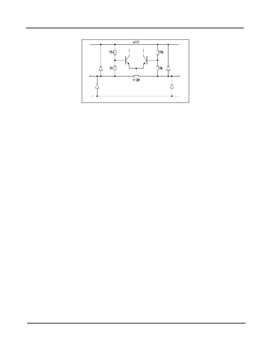
Figure 20 - LVDS Input (EN2, /EN2), (EN3, /EN3), (EN4, /EN4)
ZL40539
Data Sheet
22
Zarlink Semiconductor Inc.
OUTA and OUTB Control
Table 1 - Output Function for Set Logic Inputs
Note: 1 = logic high, 0 = logic low and X = "don't care"
Oscillator Control
Table 2 - Output Function for Set Logic Inputs
Note: 1 = logic high, 0 = logic low and X = "don't care"
Enable
SELA
ENRB
EN2P-
EN2N
EN3P-
EN3N
EN4P-
EN4N
OUTA
OUTB
0
X
X
X
X
X
OFF
OFF
1
X
1
0
0
0
OFF
OFF
1
1
0
0
0
0
100xINR
OFF
1
1
0
1
0
0
100xINR +250xIN2
OFF
1
1
0
0
1
0
100xINR +150xIN3
OFF
1
1
0
0
0
1
100xINR +100xIN4
OFF
1
1
0
1
1
1
100xINR+250xIN2+1
50xIN3+100xIN4
OFF
1
0
0
0
0
0
OFF
100xINR
1
0
0
1
0
0
OFF
100xINR +250xIN2
1
0
0
0
1
0
OFF
100xINR +150xIN3
1
0
0
0
0
1
OFF
100xINR +100xIN4
1
0
0
1
1
1
OFF
100xINR+250xIN2+
150xIN3+100xIN4
Enable
SELA
ENRB
OSCEN
OUTA
OUTB
0
X
X
X
OFF
OFF
1
X
X
0
OFF
OFF
1
1
0
1
Frequency A,
Amplitude A
OFF
1
0
0
1
OFF
Frequency B,
Amplitude B
ZL40539
Data Sheet
23
Zarlink Semiconductor Inc.
Timing Diagrams
Figure 21 - Timing of Read or Write Channels
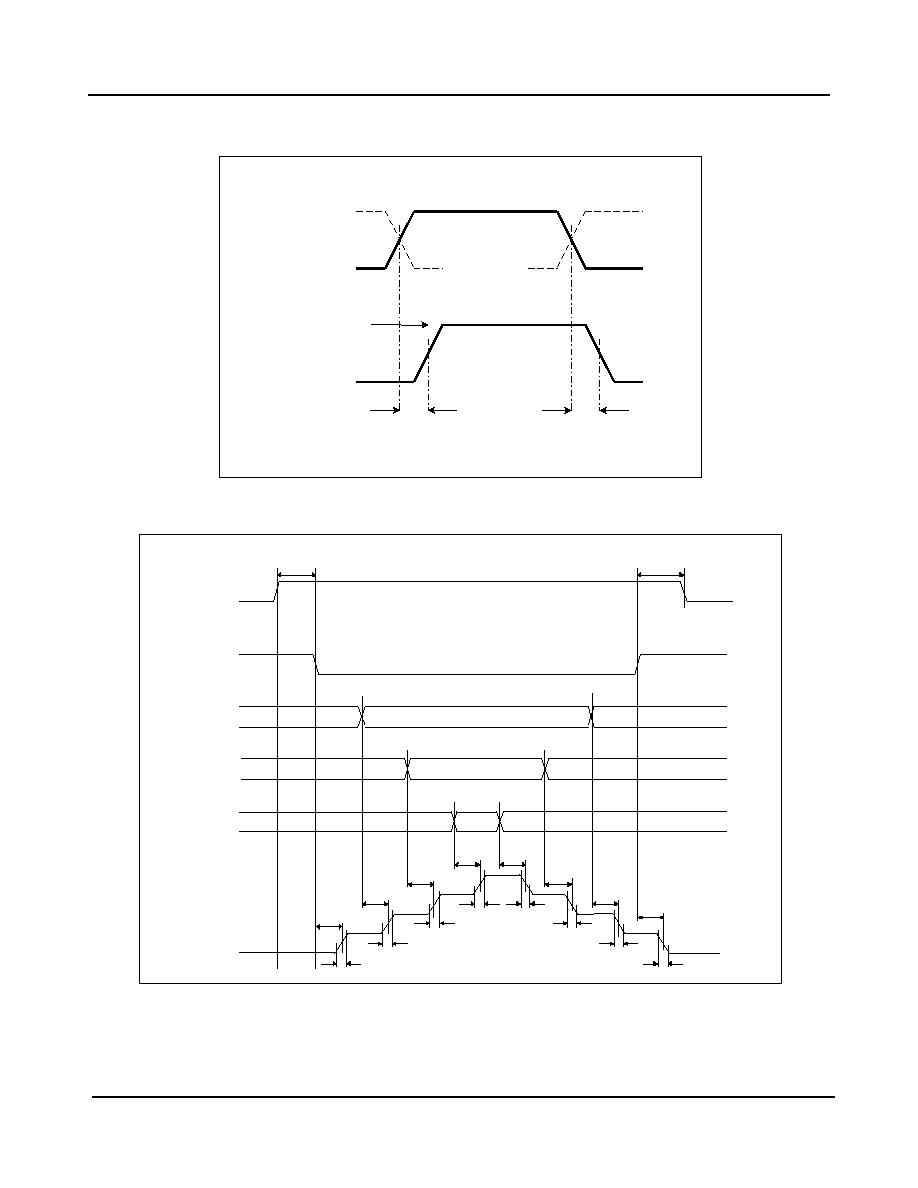
Figure 22 - Timing of Output with Enable, Read and Write Levels
EN(n)P
EN(n)N
t_on_ch
t_off_ch
Iout=IN(n)*gain
Iout=0
t
r
t
r
t
f
t
f
t
on
t
on
t
off
t
off
NE4N
ENABLE
ENRB
NE3N
NE2N
t
en
t
on
t
r
t
r
t
f
t
f
t
dis
t
off
t
off
t
on
IOUT
NE2P
NE3P
NE4P

ZL40539
Data Sheet
24
Zarlink Semiconductor Inc.
Example Waveforms
Write Waveform
The Write output waveform may be produced as shown in Figure 23. The Erase level is set by switching off both the
Bias level and the Write level. The Write switching waveform is produced by switching off the Erase level and
Switching on the Bias level and then modulating that with the Write level. The peak of the Write waveform is the
sum of the Bias and the Write levels.
Figure 23 - Write Waveform Example
Note 1: Only the Write signal changes to modulate the output during the Write pulse.
Note 2: Each of the Write Channels can provide typically 570 mA. It is not necessary to add together the output of more than one
Write Channel to achieve 570 mA.
Oscillator Waveform
The Oscillator may be enabled independently and is summed with the selected level.
Figure 24 - Example of the Oscillator Waveform Superimposed on the Read Waveform
Note: The amplitude of the Oscillator must be less than the programmed DC output level to avoid clipping and subsequent increase in
harmonic distortion.
W RITE
ERASE
BIAS
OUTPUT
BIAS
ERASE
W RITE
INPUT
ERASE
W RITE
ENRB
50%
OFF
READ
Osc_tON
Osc_tOFF
ENOSC

www.zarlink.com
Information relating to products and services furnished herein by Zarlink Semiconductor Inc. or its subsidiaries (collectively "Zarlink") is believed to be reliable.
However, Zarlink assumes no liability for errors that may appear in this publication, or for liability otherwise arising from the application or use of any such
information, product or service or for any infringement of patents or other intellectual property rights owned by third parties which may result from such application or
use. Neither the supply of such information or purchase of product or service conveys any license, either express or implied, under patents or other intellectual
property rights owned by Zarlink or licensed from third parties by Zarlink, whatsoever. Purchasers of products are also hereby notified that the use of product in
certain ways or in combination with Zarlink, or non-Zarlink furnished goods or services may infringe patents or other intellectual property rights owned by Zarlink.
This publication is issued to provide information only and (unless agreed by Zarlink in writing) may not be used, applied or reproduced for any purpose nor form part
of any order or contract nor to be regarded as a representation relating to the products or services concerned. The products, their specifications, services and other
information appearing in this publication are subject to change by Zarlink without notice. No warranty or guarantee express or implied is made regarding the
capability, performance or suitability of any product or service. Information concerning possible methods of use is provided as a guide only and does not constitute
any guarantee that such methods of use will be satisfactory in a specific piece of equipment. It is the user's responsibility to fully determine the performance and
suitability of any equipment using such information and to ensure that any publication or data used is up to date and has not been superseded. Manufacturing does
not necessarily include testing of all functions or parameters. These products are not suitable for use in any medical products whose failure to perform may result in
significant injury or death to the user. All products and materials are sold and services provided subject to Zarlink's conditions of sale which are available on request.
Purchase of Zarlink's I
2
C components conveys a licence under the Philips I
2
C Patent rights to use these components in and I
2
C System, provided that the system
conforms to the I
2
C Standard Specification as defined by Philips.
Zarlink, ZL and the Zarlink Semiconductor logo are trademarks of Zarlink Semiconductor Inc.
Copyright Zarlink Semiconductor Inc. All Rights Reserved.
TECHNICAL DOCUMENTATION - NOT FOR RESALE
For more information about all Zarlink products
visit our Web Site at