 | –≠–ª–µ–∫—Ç—Ä–æ–Ω–Ω—ã–π –∫–æ–º–ø–æ–Ω–µ–Ω—Ç: ZL40818 | –°–∫–∞—á–∞—Ç—å:  PDF PDF  ZIP ZIP |
Document Outline
- Features
- Prescaler Modulus
- Applications
- Figure 1 - Functional Block Diagram
- Description
- Figure 2 - Pin Connections - Top View
- 1.0 Application Configuration
- Figure 3 - Recommended circuit configuration.
- 2.0 Evaluation Boards From Zarlink Semiconductor
- Absolute Maximum Ratings
- AC/DC Electrical Characteristics (Tamb = 25C, Vcc = 5V) Å
- Input and Output Characteristics Å
- Figure 4 - Graph of Input Sensitivity @ +25�Deg�C
- Supply Current Table
- Input and Output Characteristics Table
- Figure 5 - Graph of Input Sensitivity @�-40, +25, +70 and +85�Deg�C.
- Figure 6 - 13.5GHz Prescalers; Phase Noise vs Offset Frequency
- Figure 7 - ZL40813; Phase Noise vs Offset Frequency
- Figure 8 - ZL40814; Phase Noise vs Offset Frequency
- Figure 9 - ZL40818; Phase Noise vs Offset Frequency
- 3.0 Single Ended Output Power.
- Figure 10 - ZL40813 (div by 8) Pout vs Input Frequency (Vcc = 4.75V)
- Figure 11 - ZL40813 (div by 8) Pout vs Input Frequency (Vcc = 5.0V)
- Figure 12 - ZL40813 (div by 8) Pout vs Input Frequency (Vcc = 5.25V)
- Figure 13 - ZL40818 (div by 4) Pout vs Input Frequency (Vcc = 4.75V)
- Figure 14 - ZL40818 (Div by 4) Pout vs Input Frequency (Vcc = 5.0V)
- Figure 15 - ZL40818 (Div by 4) Pout vs Input Frequency (Vcc = 5.25V)
- 4.0 Oscillographs of the divider output waveforms
- Figure 16 - Single-ended output waveform, showing some feedthrough of the input waveform.
- Figure 17 - Differential output waveform, showing reduced feedthrough of the input waveform
- 5.0 Application Notes
- 5.1 Application Circuit
- 5.2 Single Ended or Differential Load
1
Zarlink Semiconductor Inc.
Zarlink, ZL and the Zarlink Semiconductor logo are trademarks of Zarlink Semiconductor Inc.
Copyright 2003, Zarlink Semiconductor Inc. All Rights Reserved.
Features
∑
Very High Operating Speed
∑
Low Phase Noise (Typically better than
-146dBc/Hz at 10kHz offset)
∑
5V Single Supply Operation
∑
Low Power Dissipation: 500mW (Typ)
∑
Surface Mount Plastic Package with Exposed
Pad (See Application Notes)
Prescaler Modulus
∑
ZL40813 - Divide by 8
∑
ZL40814 - Divide by 16
∑
ZL40818 - Divide by 4
Applications
∑
10.5 to 13.5GHz PLL applications
∑
LMDS
∑
Instrumentation
∑
Satellite Communications
∑
Fibre Optic Communications; OC48, OC192
∑
Ultra Low Jitter Clock Systems
Description
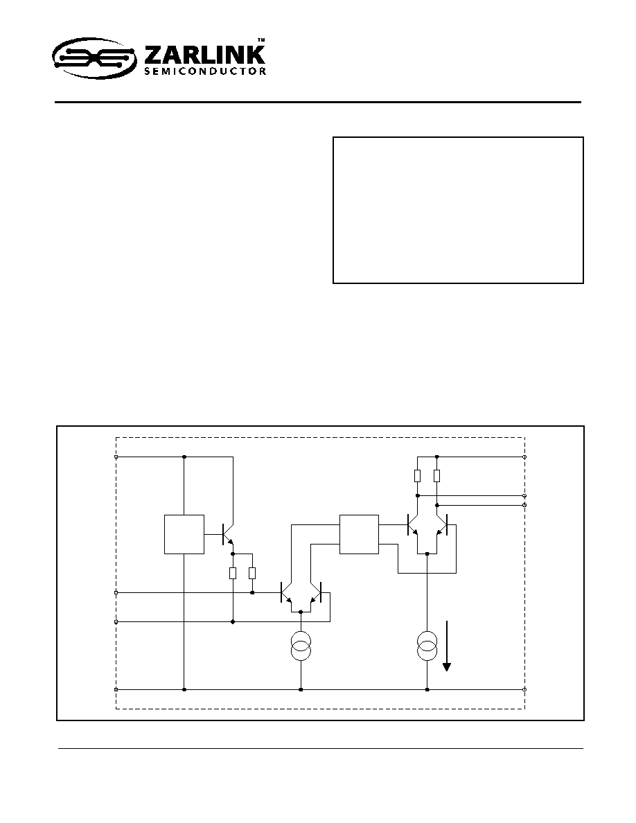
The ZL40813, 14 and 18 are 5V supply, very high
speed low power prescalers for professional
applications with a fixed modulus of 8, 16, or 4
respectively. The dividing elements are dynamic D type
flip flops and allow operation from 10.5GHz to 13.5GHz
with a sinewave input (Note these prescalers are not
suitable for D.C. operation). The output stage has
internal 50 ohm pull up giving a 1v p-p output. See
application notes for more details.
July 2003
Ordering Information
ZL40813/DCE (tubes)
8 pin SOIC
ZL40813/DCF (tape and reel) 8 pin SOIC
ZL40814/DCE (tubes)
8 pin SOIC
ZL40814/DCF (tape and reel) 8 pin SOIC
ZL40818/DCE (tubes)
8 pin SOIC
ZL40818/DCF (tape and reel) 8 pin SOIC
-40
∞
C to +85
∞
C
ZL40813/14/18
13.5GHz Fixed Modulus Dividers
Data Sheet
Figure 1 - Functional Block Diagram
Vref
Div N
20mA
50 Ohm
400 Ohm
VCC IN
VCC OUT
OUTPUT
OUTPUT B
INPUT
INPUT B
GND
GND
1
2
3
4
8
7
6
5
ZL40813/14/18
Data Sheet
2
Zarlink Semiconductor Inc.
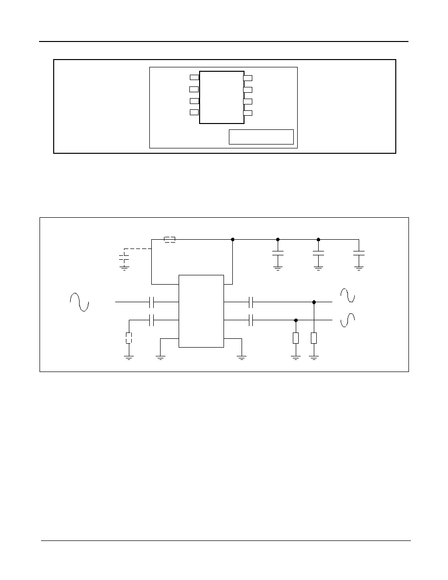
Figure 2 - Pin Connections - Top View
1.0 Application Configuration
Figure 3 shows a recommended application configuration. This example shows the devices set up for single-ended
input and differential output operation.
Figure 3 - Recommended circuit configuration.
The above circuit diagram shows some components in dotted lines. These are optional in many applications.
1. C1 (10 µF) and C2 (10 nF) power supply decoupling capacitors may be available on the board already.
2. R2 (100 Ohm) and C8 (10 nF) can be included if further power supply decoupling is required for the first stage
biasing circuit. This may optimise the noise and jitter performance. The values are suggestions and may have
to be modified if the existing supplies are particularly noisy.
3. R1 (50 Ohm), in series with C5 (100 pF), may reduce feedthrough of the input signal to the output.
Vcc INPUT
INPUT
INPUT B
GND
Vcc OUTPUT
OUTPUT
OUTPUT B
GND
1
2
3
4
5
6
7
8
SOIC (N) E-Pad
1
2
3
4
8
7
6
5
R2:100 Ohm
R1:50 Ohm
C1:10uF
C2:10nF
C3:100pF
C8:10nF
C4:100pF
C5:100pF
C6:100pF
C7:100pF
RL:50 Ohm
ZL40813/14/18
Data Sheet
3
Zarlink Semiconductor Inc.
2.0 Evaluation Boards From Zarlink Semiconductor
Zarlink Semiconductor provides prescaler evaluation boards. These are primarily for those interested in performing
their own assessment of the operation of the prescalers. The boards are supplied unpopulated and may be
assembled for single ended or differential input and output operation, type No. ZLE40008. Fully populated
evaluation boards are also available, type No. ZLE40810. Once assembled, all that is required is an RF source and
a DC supply for operation. The inputs and outputs are connected via side launch SMA connectors.
These characteristics are guaranteed by either production test or design.
Pin 1 is the Vcc pin for the 1
st
stage bias current. In some applications e.g. if the power supply is noisy, it may be advantageous to add further
supply decoupling to this pin (i.e. an additional R, C filter, see diagram of the recommended circuit configuration Figure 3,).
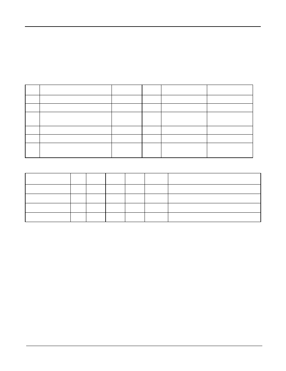
Absolute Maximum Ratings
Parameter
Symbol
Min
Max
Units
1
Supply voltage
Vcc
6.5
V
2
Prescalar Input Voltage
2.5
(vdd_IO+5%)
Vp-p
3
ESD protection (Static
Discharge)
2k
V
4
Storage Temperature
T
ST
-65
+150
∫C
5
Maximum Junction Temp.
T
J
max
+125
∫C
6
Thermal Characteristics
TH
JA
58.6
∫C/W
multi-layer PCB
AC/DC Electrical Characteristics (Tamb = 25C, Vcc = 5V)
Characteristic
Pin
Min.
Typ.
Max.
Units
Conditions
Supply current
1
0.35
mA
Input stage bias current
Supply current
8
58
93
130
mA
ZL40813 Div8
Supply current
8
61
96
134
mA
ZL40814 Div16
Supply current
8
61
100
134
mA
ZL40818 Div4
ZL40813/14/18
Data Sheet
4
Zarlink Semiconductor Inc.
These characteristics are guaranteed by either production test or design.
Input sensitivity and output power values assume 50 Ohm source and load impedances.
The device characterisation test method incremented the amplitude over the entire range of frequency and ensures that there are no "holes"
in the characteristic.
For details of the test set-up, refer to the Application Note for RF Prescalers.
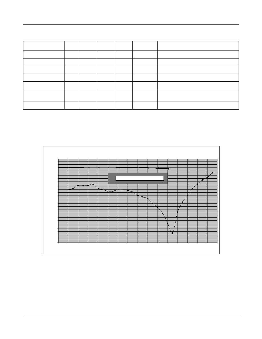
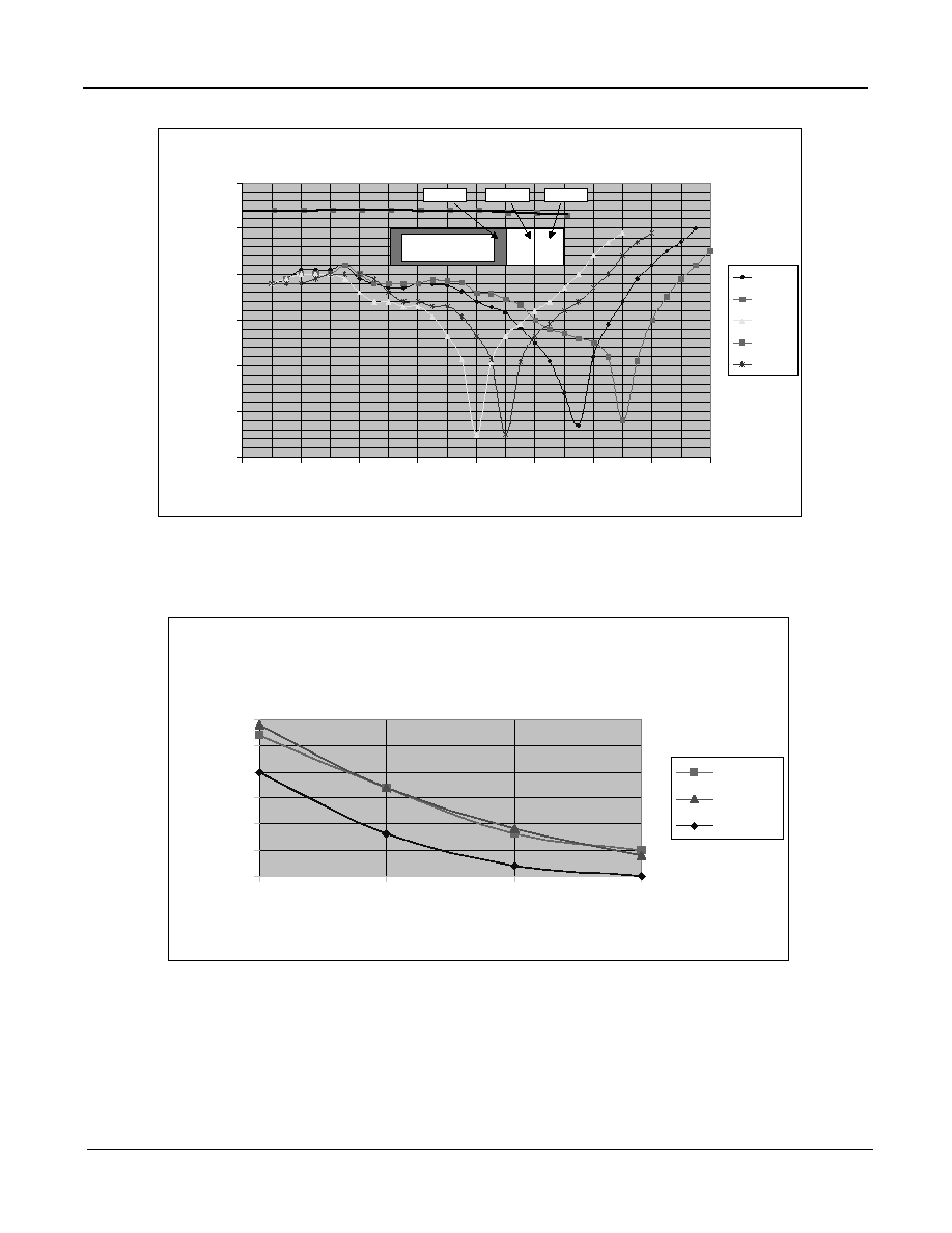
Figure 4 - Graph of Input Sensitivity @ +25 Deg C
Input and Output Characteristics
Characteristic
Pin
Min.
Typ.
Max.
Units
Conditions
Input frequency
2,3
8.5
14.5
GHz
RMS sinewave
Input sensitivity
2,3
-2
2
dBm
fin = 10.5GHz to 13.5Ghz
Input overload
2,3
10
14
dBm
fin = 10.5GHz to 13.5Ghz
Output voltage
6,7
1
Vp-p
Differential Into 50ohm pullup resistors
Output power
6,7
-6
-1
dBm
fin = 10.5GHz to 13.5GHz
Phase Noise
(10kHz offset)
6,7
-140
dBc/Hz
fin = 10GHz, pwr ip = 0dBm
See graphs, Figure 7 to Figure 9
O/P Duty Cycle
6,7
45
50
55
%
Differential output
ZL40814 Typical I nput Sensitivity (Sinewave Drive) @ +25DegC
-40.00
-30.00
-20.00
-10.00
0.00
10.00
20.00
8
9
10
11
12
13
14
15
16
Frequency (GHz)
Vin
i
n
t
o
5
0
O
h
m
(
d
B
m
)
Guaranteed Operating Window

ZL40813/14/18
Data Sheet
5
Zarlink Semiconductor Inc.
Electrical Characteristics (Vcc = 5V ±5%, Tamb = -40 to +85C)
The following characteristics are guaranteed by design and characterisation over the range of operating conditions
unless otherwise stated:
(Input Frequency range 9 to 13.5GHz rms Sinewave)
Pin 1 is the Vcc pin for the 1
st
stage bias current. In some applications e.g. if the power supply is noisy, it may be advantageous to add further
supply decoupling to this pin (i.e. an additional R, C filter, see diagram of the recommended circuit configuration, Figure 9).
For details of the test set-up, refer to the Application Note for RF Prescalers.
Supply Current Table
Characteristic
Pin
Min.
Typ.
Max.
Units
Conditions
Supply current
1
0.35
mA
Input stage bias current
Supply current
8
51
93
144
mA
ZL40813
Supply current
8
54
96
148
mA
ZL40814
Supply current
8
54
100
148
mA
ZL40818
Input and Output Characteristics Table
Input sensitivity and output power values assume 50 Ohm source and load impedances
Characteristic
Pin
Min.
Typ.
Max.
Units
Conditions
Input sensitivity
2,3
-2
2
dBm
fin = 10.5 to 12.5 GHz
Input sensitivity
2,3
10
14
dBm
fin = 10.5 to 13.5 GHz
Output voltage
6,7
1
Vp-p
Differential Into 50ohm pullup
resistors
Output power
6,7
-6
0
5
dBm
Single-ended output, fin = 9GHz to
13GHz, pwr ip= -10dBm .
See graphs, Figure 7 to Figure 9.
O/P Duty Cycle
6,7
45
50
55
%
Trise and Tfall
6,7
110
ps
ZL40813/14/18
Data Sheet
6
Zarlink Semiconductor Inc.
Figure 5 - Graph of Input Sensitivity @ -40, +25, +70 and +85 Deg C.
Figure 6 - 13.5GHz Prescalers; Phase Noise vs Offset Frequency
ZL40814 Typical Input Sensitivity (Sinewave Drive) @ -40 to +85 DegC
-40.00
-30.00
-20.00
-10.00
0.00
10.00
20.00
8
9
10
11
12
13
14
15
16
Input Frequency (GHz)
Vi
n
i
n
t
o
5
0
O
h
m
(
d
B
m
)
25C
-40C
85C
Max
70C
Guaranteed Operating
W indow
85 DegC
70 DegC
25 DegC
Phase Noise vs Offset Freq in = 10GHz
Pin = -1dBm, 5.25V, Temp = 25C
-150
-145
-140
-135
-130
-125
-120
0.1
1
10
100
Offset Frequency in kHz
Ph
ase N
o
i
se i
n
d
B
c/
H
z
ZL40818
ZL40813
ZL40814
ZL40813/14/18
Data Sheet
7
Zarlink Semiconductor Inc.
Figure 7 - ZL40813; Phase Noise vs Offset Frequency
Figure 8 - ZL40814; Phase Noise vs Offset Frequency
ZL40813 Phase Noise vs Offset
Pin = -1dBm, 5.25V, Temp = 25C
-150
-145
-140
-135
-130
-125
-120
0.1
1
10
100
Offset Frequency in kHz
P
h
a
se N
o
i
s
e i
n
d
B
c/
H
z
10GHz
12GHz
ZL40814 Phase Noise vs Offset
Pin = -1dBm, 5.25V, Temp = 25C
-150
-145
-140
-135
-130
-125
-120
0.1
1
10
100
Offset Frequency in kHz
P
h
ase N
o
i
s
e i
n
d
B
c/
H
z
13GHz
12GHz
10GHz

ZL40813/14/18
Data Sheet
8
Zarlink Semiconductor Inc.
Figure 9 - ZL40818; Phase Noise vs Offset Frequency
3.0 Single Ended Output Power.
The following graphs show how the output power varies with supply.
Differential power will be 3dB greater.
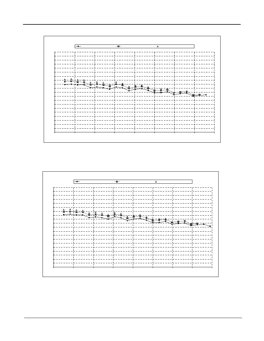
Figure 10 - ZL40813 (div by 8) Pout vs Input Frequency (Vcc = 4.75V)
ZL40818 Phase Noise vs Offset
Pin = -1dBm, 5.25V, Temp = 25C
-150
-145
-140
-135
-130
-125
-120
0.1
1
10
100
Offset Frequency in kHz
P
h
ase N
o
i
se i
n
d
B
c
/
H
z
10GHz
12GHz
Frequency_sweep , Vcc = 4 .75v
-15
-14
-13
-12
-11
-10
-9
-8
-7
-6
-5
-4
-3
-2
-1
0
1
2
3
4
5
8.0E+9
9.0 E+9
10.0E+9
11 .0E+9
12.0 E+9
13.0E+9
14.0 E+9
1 5.0E+9
16.0E+9
i/p frequency (H z)
o/
p
l
e
v
e
l
(
d
B
m
)
Device 1 ,Temperature = -40∞C
Device 1,Temperature = 2 5∞C
D evice 1,Temperature = 85∞C

ZL40813/14/18
Data Sheet
9
Zarlink Semiconductor Inc.
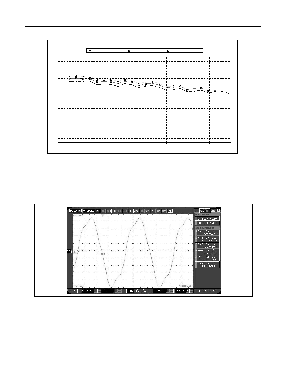
Figure 11 - ZL40813 (div by 8) Pout vs Input Frequency (Vcc = 5.0V)
Figure 12 - ZL40813 (div by 8) Pout vs Input Frequency (Vcc = 5.25V)
Frequency_sweep, Vcc = 5v
-15
-14
-13
-12
-11
-10
-9
-8
-7
-6
-5
-4
-3
-2
-1
0
1
2
3
4
5
8.0E+9
9.0 E+9
10.0E+9
11 .0E+9
12.0 E+9
13.0E+9
14.0 E+9
1 5.0E+9
16.0E+9
i/p frequency (H z)
o/
p
l
e
v
e
l
(
d
B
m
)
Device 1 ,Temperature = -40∞C
Device 1,Temperature = 2 5∞C
D evice 1,Temperature = 85∞C
Frequency_sweep, Vcc = 5.25v
-15
-14
-13
-12
-11
-10
-9
-8
-7
-6
-5
-4
-3
-2
-1
0
1
2
3
4
5
8.0E+9
9.0E+9
10.0E+9
11.0E+9
12.0E+9
13.0E+9
14.0E+9
15.0E+9
16.0E+9
i/p f requency (H z)
o/
p l
e
v
e
l
(
d
B
m
)
Device 1,Temperature = -40∞C
Device 1,Temperature = 25∞C
D evice 1,Tem perature = 85∞C
ZL40813/14/18
Data Sheet
10
Zarlink Semiconductor Inc.
Figure 13 - ZL40818 (div by 4) Pout vs Input Frequency (Vcc = 4.75V)
Figure 14 - ZL40818 (Div by 4) Pout vs Input Frequency (Vcc = 5.0V)
Frequency_sweep, Vcc = 4.75v
-15
-14
-13
-12
-11
-10
-9
-8
-7
-6
-5
-4
-3
-2
-1
0
1
2
3
4
5
8.0E+9
9.0E+9
10.0E+9
11.0E+9
12.0E+9
13.0E+9
14.0E+9
15.0E+9
16. 0E+9
i/p f requency (H z)
o/
p l
e
v
e
l
(
d
B
m
)
Device 1,Temperature = -40∞C
Device 1,Temperature = 25∞C
D evice 1,Temperature = 85∞C
Frequency_sweep, Vcc = 5v
-15
-14
-13
-12
-11
-10
-9
-8
-7
-6
-5
-4
-3
-2
-1
0
1
2
3
4
5
8.0E+9
9.0 E+9
10.0E+9
11 .0E+9
12.0 E+9
13.0E+9
14.0 E+9
1 5.0E+9
16.0E+9
i/p frequency (H z)
o/
p l
e
v
e
l
(
d
B
m
)
Device 1 ,Temperature = -40∞C
Device 1,Temperature = 2 5∞C
D evice 1,Temperature = 85∞C
ZL40813/14/18
Data Sheet
11
Zarlink Semiconductor Inc.
Figure 15 - ZL40818 (Div by 4) Pout vs Input Frequency (Vcc = 5.25V)
4.0 Oscillographs of the divider output waveforms
The following oscillographs show that the low-level feedthrough of the input waveform can be further reduced by
summing the two output pins of the device differentially, refer to Figure 16 and Figure 17.
Figure 16 - Single-ended output waveform, showing some feedthrough of the input waveform.
VCC = 5V, Vin = 2dBm, Fin = 10GHz.
Frequency_sweep, Vcc = 5.25v
-15
-14
-13
-12
-11
-10
-9
-8
-7
-6
-5
-4
-3
-2
-1
0
1
2
3
4
5
8.0E+9
9.0E+9
10.0E+9
11.0E+9
12.0E+9
13.0E+9
14.0E+9
15.0E+9
16.0E+9
i/p frequency (Hz)
o/
p
l
e
v
e
l
(
d
B
m
)
Device 1,Temperature = -40∞C
Device 1,Temperature = 25∞C
Device 1,Temperature = 85∞C

ZL40813/14/18
Data Sheet
12
Zarlink Semiconductor Inc.
Figure 17 - Differential output waveform, showing reduced feedthrough of the input waveform
VCC = 5V, Vin = 2dBm, Fin = 10GHz.
5.0 Application Notes
5.1 Application Circuit
Figure 3 illustrates the recommended Single Ended Application Circuit. This represents the circuit used to complete
characterisation. The tabulated Electrical performance is guaranteed using this application circuit.
A blank application board is available.
5.1.1 Circuit Options
The application circuit includes some optional components that may be required to improve tolerance of system
noise present in the application.
Dummy R source may be added to the inverting input to provide a better matched source impedance at the input.
This will improve the rejection of common mode noise present within the system.
Dummy R load may be added to the inverting output to provide better matched load at the output. This will reduce
the radiated EMI at the output and reduce the Output Noise present on the supply rail.
Rfilter can be inserted between the Vcc in and the Vcc_out to provide additional filtering to the input Vcc. The input
Vcc powers the input bias reference only and can be a sensitive point to system noise. The nominal input current at
Vcc_IN s 0.35mA. An alternative would be to use an inductive choke.
C1 is additional Supply Filtering and should be added with Rfilter. The IC includes 10pF of on Chip Supply Filtering.

ZL40813/14/18
Data Sheet
13
Zarlink Semiconductor Inc.
5.2 Single Ended or Differential Load
Figure 16 and Figure 17 illustrate the output waveform when measured differential and single ended with a 10GHz
waveform at the input at a level of +2dBm. The single ended output contains some input frequency break through
which contributes to the distortion present. This is a common mode signal which is rejected if the output is taken
differentially.
Differential operation also provides an additional 3dBV output power.
Differential Operation reduces the radiated EMI in the system and reduces the susceptibility to common mode
system noise.
NOTE: It is strongly recommended that these devices are used differentially for all applications.
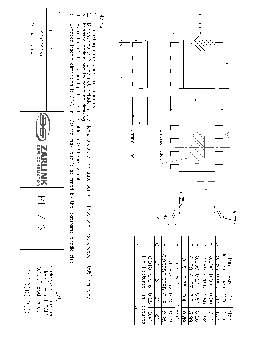
c Zarlink Semiconductor 2003 All rights reserved.
APPRD.
ISSUE
DATE
ACN
Package Code
Previous package codes

www.zarlink.com
Information relating to products and services furnished herein by Zarlink Semiconductor Inc. or its subsidiaries (collectively "Zarlink") is believed to be reliable.
However, Zarlink assumes no liability for errors that may appear in this publication, or for liability otherwise arising from the application or use of any such
information, product or service or for any infringement of patents or other intellectual property rights owned by third parties which may result from such application or
use. Neither the supply of such information or purchase of product or service conveys any license, either express or implied, under patents or other intellectual
property rights owned by Zarlink or licensed from third parties by Zarlink, whatsoever. Purchasers of products are also hereby notified that the use of product in
certain ways or in combination with Zarlink, or non-Zarlink furnished goods or services may infringe patents or other intellectual property rights owned by Zarlink.
This publication is issued to provide information only and (unless agreed by Zarlink in writing) may not be used, applied or reproduced for any purpose nor form part
of any order or contract nor to be regarded as a representation relating to the products or services concerned. The products, their specifications, services and other
information appearing in this publication are subject to change by Zarlink without notice. No warranty or guarantee express or implied is made regarding the
capability, performance or suitability of any product or service. Information concerning possible methods of use is provided as a guide only and does not constitute
any guarantee that such methods of use will be satisfactory in a specific piece of equipment. It is the user's responsibility to fully determine the performance and
suitability of any equipment using such information and to ensure that any publication or data used is up to date and has not been superseded. Manufacturing does
not necessarily include testing of all functions or parameters. These products are not suitable for use in any medical products whose failure to perform may result in
significant injury or death to the user. All products and materials are sold and services provided subject to Zarlink's conditions of sale which are available on request.
Purchase of Zarlink's I
2
C components conveys a licence under the Philips I
2
C Patent rights to use these components in and I
2
C System, provided that the system
conforms to the I
2
C Standard Specification as defined by Philips.
Zarlink, ZL and the Zarlink Semiconductor logo are trademarks of Zarlink Semiconductor Inc.
Copyright Zarlink Semiconductor Inc. All Rights Reserved.
TECHNICAL DOCUMENTATION - NOT FOR RESALE
For more information about all Zarlink products
visit our Web Site at