
1
Zarlink Semiconductor Inc.
Zarlink, ZL and the Zarlink Semiconductor logo are trademarks of Zarlink Semiconductor Inc.
Copyright 2003-2004, Zarlink Semiconductor Inc. All Rights Reserved.
Features
�
512 channel x 512 channel non-blocking switch
at 2.048 Mbps, 4.096 Mbps or 8.192 Mbps
operation
�
Rate conversion between the ST-BUS inputs and
ST-BUS outputs
�
Integrated Digital Phase-Locked Loop (DPLL)
meets Telcordia GR-1244-CORE Stratum 4
enhanced specifications
�
DPLL provides automatic reference switching,
jitter attenuation, holdover and free run functions
�
Per-stream ST-BUS input with data rate selection
of 2.048 Mbps, 4.096 Mbps or 8.192 Mbps
�
Per-stream ST-BUS output with data rate
selection of 2.048 Mbps, 4.096 Mbps or
8.192 Mbps; the output data rate can be different
than the input data rate
�
Per-stream high impedance control output for
every ST-BUS output with fractional bit
advancement
�
Per-stream input channel and input bit delay
programming with fractional bit delay
�
Per-stream output channel and output bit delay
programming with fractional bit advancement
�
Multiple frame pulse outputs and reference clock
outputs
�
Per-channel constant throughput delay
�
Per-channel high impedance output control
�
Per-channel message mode
�
Per-channel Pseudo Random Bit Sequence
(PRBS) pattern generation and bit error detection
�
Control interface compatible to Motorola non-
multiplexed CPUs
�
Connection memory block programming
capability
�
IEEE-1149.1 (JTAG) test port
�
3.3 V I/O with 5 V tolerant input
July 2004
Ordering Information
ZL50010/QCC 160 Pin LQFP
ZL50010/GDC 144 Ball LBGA
-40
�
C to +85
�
C
ZL50010
Flexible 512 Channel DX with Enhanced
DPLL
Data Sheet
Figure 1 - ZL50010 Functional Block Diagram
Zarlink Semiconductor US Patent No. 5,602,884, UK Patent No. 0772912,
France Brevete S.G.D.G. 0772912; Germany DBP No. 69502724.7-08
DS
CS
R/
W
A1
1 -
0
DTA
D15
-
0
Test Port
Microprocessor
Interface
V
SS
V
DD
TD
I
TDO
TCK
TR
ST
TM
S
STo0-15
RESET
Connection Memory
CKo1
STi0-15
APLL
FPo1
ODE
Input Timing
Data Memory
S/P Converter
P/S Converter
Output HiZ Control
STOHZ0-15
CKo0
FPo0
CKo2
FPo2
CKi
FPi
OSC
XT
A
L
o
XT
A
L
i
DPLL
PRI_REF
and
Internal
Registers
Output Timing
SG
1
TM
1
TM
2
CLKBYPS
IC0 - 4
SEC_REF
V
SS_A
P
LL
V
DD
_APLL

ZL50010
Data Sheet
2
Zarlink Semiconductor Inc.
Applications
�
Small and medium digital switching platforms
�
Access Servers
�
Time Division Multiplexers
�
Computer Telephony Integration
�
Digital Loop Carriers
Description
The device has 16 ST-BUS inputs (STi0-15) and 16 ST-BUS outputs (STo0-15). It is a non-blocking digital switch
with 512 64 kbps channels and performs rate conversion between the ST-BUS inputs and ST-BUS outputs. The
ST-BUS inputs accept serial input data streams with the data rate of 2.048 Mbps, 4.096 Mbps or 8.192 Mbps on a
per-stream basis. The ST-BUS outputs deliver serial output data streams with the data rate of 2.048 Mbps,
4.096 Mbps or 8.192 Mbps on a per-stream basis. The device also provides 16 high impedance control outputs
(STOHZ 0-15) to support the use of external high impedance control buffers.
The ZL50010 has features that are programmable on a per-stream or per-channel basis including message mode,
input bit delay, output bit advancement, constant throughput delay and high impedance output control.
The on-chip DPLL meets Telcordia GR-1244-CORE Stratum 4 enhanced specifications (Stratum 4E). It accepts
two dedicated timing reference inputs at either 8 kHz, 1.544 MHz or 2.048 MHz. Alternatively, one reference can be
replaced by an internal 8 kHz signal derived from the ST-BUS input frame boundary. The DPLL provides automatic
reference switching, jitter attenuation, holdover and free run functions. It can be used as a system's ST-BUS timing
source which is synchronized to the network. The DPLL can also be bypassed so that the device operates under
system timing.

ZL50010
Data Sheet
Table of Contents
3
Zarlink Semiconductor Inc.
Features . . . . . . . . . . . . . . . . . . . . . . . . . . . . . . . . . . . . . . . . . . . . . . . . . . . . . . . . . . . . . . . . . . . . . . . . . . . . . . . . . 1
Applications . . . . . . . . . . . . . . . . . . . . . . . . . . . . . . . . . . . . . . . . . . . . . . . . . . . . . . . . . . . . . . . . . . . . . . . . . . . . . 2
Description . . . . . . . . . . . . . . . . . . . . . . . . . . . . . . . . . . . . . . . . . . . . . . . . . . . . . . . . . . . . . . . . . . . . . . . . . . . . . . 2
1.0 Device Overview . . . . . . . . . . . . . . . . . . . . . . . . . . . . . . . . . . . . . . . . . . . . . . . . . . . . . . . . . . . . . . . . . . . . . . 15
2.0 Functional Description . . . . . . . . . . . . . . . . . . . . . . . . . . . . . . . . . . . . . . . . . . . . . . . . . . . . . . . . . . . . . . . . . 15
2.1 ST-BUS Input Data Rate and Input Timing . . . . . . . . . . . . . . . . . . . . . . . . . . . . . . . . . . . . . . . . . . . . . . . . 15
2.1.1 ST-BUS Input Operation Mode . . . . . . . . . . . . . . . . . . . . . . . . . . . . . . . . . . . . . . . . . . . . . . . . . . . . 15
2.1.2 Frame Pulse Input and Clock Input Timing . . . . . . . . . . . . . . . . . . . . . . . . . . . . . . . . . . . . . . . . . . . 15
2.1.3 ST-BUS Input Timing . . . . . . . . . . . . . . . . . . . . . . . . . . . . . . . . . . . . . . . . . . . . . . . . . . . . . . . . . . . . 17
2.2 ST-BUS Output Data Rate and Output Timing . . . . . . . . . . . . . . . . . . . . . . . . . . . . . . . . . . . . . . . . . . . . . 18
2.2.1 ST-BUS Output Operation Mode . . . . . . . . . . . . . . . . . . . . . . . . . . . . . . . . . . . . . . . . . . . . . . . . . . . 18
2.2.2 Frame Pulse Output and Clock Output Timing . . . . . . . . . . . . . . . . . . . . . . . . . . . . . . . . . . . . . . . . 18
2.2.3 ST-BUS Output Timing . . . . . . . . . . . . . . . . . . . . . . . . . . . . . . . . . . . . . . . . . . . . . . . . . . . . . . . . . . 21
2.3 Serial Data Input Delay and Serial Data Output Offset . . . . . . . . . . . . . . . . . . . . . . . . . . . . . . . . . . . . . . . 22
2.3.1 Input Channel Delay Programming . . . . . . . . . . . . . . . . . . . . . . . . . . . . . . . . . . . . . . . . . . . . . . . . . 22
2.3.2 Input Bit Delay Programming . . . . . . . . . . . . . . . . . . . . . . . . . . . . . . . . . . . . . . . . . . . . . . . . . . . . . . 22
2.3.3 Fractional Input Bit Delay Programming . . . . . . . . . . . . . . . . . . . . . . . . . . . . . . . . . . . . . . . . . . . . . 23
2.3.4 Output Channel Delay Programming . . . . . . . . . . . . . . . . . . . . . . . . . . . . . . . . . . . . . . . . . . . . . . . . 23
2.3.5 Output Bit Delay Programming . . . . . . . . . . . . . . . . . . . . . . . . . . . . . . . . . . . . . . . . . . . . . . . . . . . . 24
2.3.6 Fractional Output Bit Advancement Programming. . . . . . . . . . . . . . . . . . . . . . . . . . . . . . . . . . . . . . 24
2.3.7 External High Impedance Control, STOHZ 0 to 15 . . . . . . . . . . . . . . . . . . . . . . . . . . . . . . . . . . . . . 25
2.4 Data Delay Through The Switching Paths. . . . . . . . . . . . . . . . . . . . . . . . . . . . . . . . . . . . . . . . . . . . . . . . . 26
2.5 Connection Memory Description . . . . . . . . . . . . . . . . . . . . . . . . . . . . . . . . . . . . . . . . . . . . . . . . . . . . . . . . 28
2.5.1 Connection Memory Block Programming. . . . . . . . . . . . . . . . . . . . . . . . . . . . . . . . . . . . . . . . . . . . . 28
2.6 Bit Error Rate (BER) Test . . . . . . . . . . . . . . . . . . . . . . . . . . . . . . . . . . . . . . . . . . . . . . . . . . . . . . . . . . . . . 29
2.7 Quadrant frame programming . . . . . . . . . . . . . . . . . . . . . . . . . . . . . . . . . . . . . . . . . . . . . . . . . . . . . . . . . . 30
2.8 Microprocessor Port . . . . . . . . . . . . . . . . . . . . . . . . . . . . . . . . . . . . . . . . . . . . . . . . . . . . . . . . . . . . . . . . . 31
2.9 Digital Phase-Locked Loop (DPLL) Operation . . . . . . . . . . . . . . . . . . . . . . . . . . . . . . . . . . . . . . . . . . . . . 31
2.9.1 DPLL Master Mode . . . . . . . . . . . . . . . . . . . . . . . . . . . . . . . . . . . . . . . . . . . . . . . . . . . . . . . . . . . . . 32
2.9.1.1 Master Mode Reference Inputs . . . . . . . . . . . . . . . . . . . . . . . . . . . . . . . . . . . . . . . . . . . . . . . 32
2.9.1.2 Master Mode Reference Switching. . . . . . . . . . . . . . . . . . . . . . . . . . . . . . . . . . . . . . . . . . . . . 33
2.9.1.3 DPLL Status Reporting. . . . . . . . . . . . . . . . . . . . . . . . . . . . . . . . . . . . . . . . . . . . . . . . . . . . . . 33
2.9.1.4 Master Mode Output Offset Adjustment . . . . . . . . . . . . . . . . . . . . . . . . . . . . . . . . . . . . . . . . . 33
2.9.2 DPLL Freerun Mode. . . . . . . . . . . . . . . . . . . . . . . . . . . . . . . . . . . . . . . . . . . . . . . . . . . . . . . . . . . . . 34
2.9.3 DPLL Bypass Mode . . . . . . . . . . . . . . . . . . . . . . . . . . . . . . . . . . . . . . . . . . . . . . . . . . . . . . . . . . . . . 34
2.10 DPLL Functional Description . . . . . . . . . . . . . . . . . . . . . . . . . . . . . . . . . . . . . . . . . . . . . . . . . . . . . . . . . . 35
2.10.1 CKi/FPi Synchronizer and PRI_REF Select Mux Circuits . . . . . . . . . . . . . . . . . . . . . . . . . . . . . . . 35
2.10.2 Reference Select and Frequency Mode Mux Circuits . . . . . . . . . . . . . . . . . . . . . . . . . . . . . . . . . . 36
2.10.3 Skew Control Circuit. . . . . . . . . . . . . . . . . . . . . . . . . . . . . . . . . . . . . . . . . . . . . . . . . . . . . . . . . . . . 36
2.10.4 Reference Monitor Circuit . . . . . . . . . . . . . . . . . . . . . . . . . . . . . . . . . . . . . . . . . . . . . . . . . . . . . . . 36
2.10.5 LOS Control Circuit . . . . . . . . . . . . . . . . . . . . . . . . . . . . . . . . . . . . . . . . . . . . . . . . . . . . . . . . . . . . 37
2.10.6 State Machine Circuit . . . . . . . . . . . . . . . . . . . . . . . . . . . . . . . . . . . . . . . . . . . . . . . . . . . . . . . . . . . 37
2.10.7 Maximum Time Interval Error (MTIE) Circuit . . . . . . . . . . . . . . . . . . . . . . . . . . . . . . . . . . . . . . . . . 38
2.10.8 Phase-Locked Loop (PLL) Circuit . . . . . . . . . . . . . . . . . . . . . . . . . . . . . . . . . . . . . . . . . . . . . . . . . 38
2.11 DPLL Performance . . . . . . . . . . . . . . . . . . . . . . . . . . . . . . . . . . . . . . . . . . . . . . . . . . . . . . . . . . . . . . . . . 40
2.11.1 Intrinsic Jitter . . . . . . . . . . . . . . . . . . . . . . . . . . . . . . . . . . . . . . . . . . . . . . . . . . . . . . . . . . . . . . . . . 40
2.11.2 Jitter Tolerance . . . . . . . . . . . . . . . . . . . . . . . . . . . . . . . . . . . . . . . . . . . . . . . . . . . . . . . . . . . . . . . 40
2.11.3 Jitter Transfer . . . . . . . . . . . . . . . . . . . . . . . . . . . . . . . . . . . . . . . . . . . . . . . . . . . . . . . . . . . . . . . . . 40
2.11.4 Frequency Accuracy . . . . . . . . . . . . . . . . . . . . . . . . . . . . . . . . . . . . . . . . . . . . . . . . . . . . . . . . . . . 40
2.11.5 Holdover Accuracy . . . . . . . . . . . . . . . . . . . . . . . . . . . . . . . . . . . . . . . . . . . . . . . . . . . . . . . . . . . . . 42
2.11.6 Locking Range . . . . . . . . . . . . . . . . . . . . . . . . . . . . . . . . . . . . . . . . . . . . . . . . . . . . . . . . . . . . . . . . 42
2.11.7 Phase Slope. . . . . . . . . . . . . . . . . . . . . . . . . . . . . . . . . . . . . . . . . . . . . . . . . . . . . . . . . . . . . . . . . . 42

ZL50010
Data Sheet
Table of Contents
4
Zarlink Semiconductor Inc.
2.11.8 MTIE. . . . . . . . . . . . . . . . . . . . . . . . . . . . . . . . . . . . . . . . . . . . . . . . . . . . . . . . . . . . . . . . . . . . . . . . 42
2.11.9 Phase Lock Time . . . . . . . . . . . . . . . . . . . . . . . . . . . . . . . . . . . . . . . . . . . . . . . . . . . . . . . . . . . . . . 43
2.12 Alignment Between Input and Output Frame Pulses. . . . . . . . . . . . . . . . . . . . . . . . . . . . . . . . . . . . . . . . 43
3.0 Oscillator Requirements . . . . . . . . . . . . . . . . . . . . . . . . . . . . . . . . . . . . . . . . . . . . . . . . . . . . . . . . . . . . . . . . 44
3.1 External Crystal Oscillator . . . . . . . . . . . . . . . . . . . . . . . . . . . . . . . . . . . . . . . . . . . . . . . . . . . . . . . . . . . . . 44
3.2 External Clock Oscillator . . . . . . . . . . . . . . . . . . . . . . . . . . . . . . . . . . . . . . . . . . . . . . . . . . . . . . . . . . . . . . 45
4.0 Device Reset and Initialization . . . . . . . . . . . . . . . . . . . . . . . . . . . . . . . . . . . . . . . . . . . . . . . . . . . . . . . . . . . 46
5.0 JTAG Support. . . . . . . . . . . . . . . . . . . . . . . . . . . . . . . . . . . . . . . . . . . . . . . . . . . . . . . . . . . . . . . . . . . . . . . . . 46
5.1 Test Access Port (TAP) . . . . . . . . . . . . . . . . . . . . . . . . . . . . . . . . . . . . . . . . . . . . . . . . . . . . . . . . . . . . . . . 46
5.2 Instruction Register . . . . . . . . . . . . . . . . . . . . . . . . . . . . . . . . . . . . . . . . . . . . . . . . . . . . . . . . . . . . . . . . . . 47
5.3 Test Data Register. . . . . . . . . . . . . . . . . . . . . . . . . . . . . . . . . . . . . . . . . . . . . . . . . . . . . . . . . . . . . . . . . . . 47
5.4 BSDL . . . . . . . . . . . . . . . . . . . . . . . . . . . . . . . . . . . . . . . . . . . . . . . . . . . . . . . . . . . . . . . . . . . . . . . . . . . . . 47
6.0 Register Address Mapping . . . . . . . . . . . . . . . . . . . . . . . . . . . . . . . . . . . . . . . . . . . . . . . . . . . . . . . . . . . . . . 48
7.0 Detail Register description . . . . . . . . . . . . . . . . . . . . . . . . . . . . . . . . . . . . . . . . . . . . . . . . . . . . . . . . . . . . . . 50
8.0 Memory Address Mappings . . . . . . . . . . . . . . . . . . . . . . . . . . . . . . . . . . . . . . . . . . . . . . . . . . . . . . . . . . . . . 68
9.0 Connection Memory Bit Assignment . . . . . . . . . . . . . . . . . . . . . . . . . . . . . . . . . . . . . . . . . . . . . . . . . . . . . . 69

ZL50010
Data Sheet
List of Figures
5
Zarlink Semiconductor Inc.
Figure 1 - ZL50010 Functional Block Diagram . . . . . . . . . . . . . . . . . . . . . . . . . . . . . . . . . . . . . . . . . . . . . . . . . . . . 1
Figure 2 - 24 mm x 24 mm LQFP (JEDEC MS-026) Pinout Diagram . . . . . . . . . . . . . . . . . . . . . . . . . . . . . . . . . . . 8
Figure 3 - 13 mm x 13 mm 144 Ball LBGA Pinout Diagram. . . . . . . . . . . . . . . . . . . . . . . . . . . . . . . . . . . . . . . . . . . 9
Figure 4 - Input Timing when (CKIN2 to CKIN0 Bits = 010) in the Control Register . . . . . . . . . . . . . . . . . . . . . . . 16
Figure 5 - Input Timing when (CKIN2 to CKIN0 Bits = 001) in the Control Register . . . . . . . . . . . . . . . . . . . . . . . 16
Figure 6 - Input Timing when (CKIN2 to CKIN0 Bits = 000) in the Control Register . . . . . . . . . . . . . . . . . . . . . . . 16
Figure 7 - ST-BUS Input Timing for Various Input Data Rates . . . . . . . . . . . . . . . . . . . . . . . . . . . . . . . . . . . . . . . . 17
Figure 8 - FPo0 and CKo0 Output Timing when the CKFP0 Bit = 0 . . . . . . . . . . . . . . . . . . . . . . . . . . . . . . . . . . . 19
Figure 9 - FPo0 and CKo0 Output Timing when the CKFP0 Bit = 1 . . . . . . . . . . . . . . . . . . . . . . . . . . . . . . . . . . . 19
Figure 10 - FPo1 and CKo1 Output Timing when the CKFP1 Bit = 0 . . . . . . . . . . . . . . . . . . . . . . . . . . . . . . . . . . 19
Figure 11 - FPo1 and CKo1 Output Timing when the CKFP1 Bit = 1 . . . . . . . . . . . . . . . . . . . . . . . . . . . . . . . . . . 19
Figure 12 - FPo2 and CKo2 Output Timing when the CKFP2 Bit = 0 . . . . . . . . . . . . . . . . . . . . . . . . . . . . . . . . . . 20
Figure 13 - FPo2 and CKo2 Output Timing when the CKFP2 Bit = 1 . . . . . . . . . . . . . . . . . . . . . . . . . . . . . . . . . . 20
Figure 14 - ST-BUS Output Timing for Various Output Data Rates . . . . . . . . . . . . . . . . . . . . . . . . . . . . . . . . . . . . 21
Figure 15 - Input Channel Delay Timing Diagram . . . . . . . . . . . . . . . . . . . . . . . . . . . . . . . . . . . . . . . . . . . . . . . . . 22
Figure 16 - Input Bit Delay Timing Diagram . . . . . . . . . . . . . . . . . . . . . . . . . . . . . . . . . . . . . . . . . . . . . . . . . . . . . . 23
Figure 17 - Output Channel Delay Timing Diagram . . . . . . . . . . . . . . . . . . . . . . . . . . . . . . . . . . . . . . . . . . . . . . . . 23
Figure 18 - Output Bit Delay Timing Diagram . . . . . . . . . . . . . . . . . . . . . . . . . . . . . . . . . . . . . . . . . . . . . . . . . . . . 24
Figure 19 - Fractional Output Bit Advancement Timing Diagram. . . . . . . . . . . . . . . . . . . . . . . . . . . . . . . . . . . . . . 24
Figure 20 - Example: External High Impedance Control Timing . . . . . . . . . . . . . . . . . . . . . . . . . . . . . . . . . . . . . . 25
Figure 21 - Data Throughput Delay when Input and Output Channel Delay are Disabled for Input Ch0 Switched to
Output Ch0 . . . . . . . . . . . . . . . . . . . . . . . . . . . . . . . . . . . . . . . . . . . . . . . . . . . . . . . . . . . . . . . . . . . . . . 27
Figure 22 - Data Throughput Delay when Input Channel Delay is Enabled and Output Channel Delay is Disabled
for Input Ch0 Switched to Output Ch0 . . . . . . . . . . . . . . . . . . . . . . . . . . . . . . . . . . . . . . . . . . . . . . . . . 27
Figure 23 - Data Throughput Delay when Input Channel Delay is Disabled and Output Channel Delay is Enabled
for Input Ch0 Switch to Output Ch0 . . . . . . . . . . . . . . . . . . . . . . . . . . . . . . . . . . . . . . . . . . . . . . . . . . . 27
Figure 24 - Data Throughput Delay when Input and Output Channel Delay are Enabled for Input Ch0 Switched to
Output Ch0 . . . . . . . . . . . . . . . . . . . . . . . . . . . . . . . . . . . . . . . . . . . . . . . . . . . . . . . . . . . . . . . . . . . . . . 28
Figure 25 - DPLL Functional Block Diagram . . . . . . . . . . . . . . . . . . . . . . . . . . . . . . . . . . . . . . . . . . . . . . . . . . . . . 35
Figure 26 - Skew Control Circuit Diagram . . . . . . . . . . . . . . . . . . . . . . . . . . . . . . . . . . . . . . . . . . . . . . . . . . . . . . . 36
Figure 27 - State Machine Diagram . . . . . . . . . . . . . . . . . . . . . . . . . . . . . . . . . . . . . . . . . . . . . . . . . . . . . . . . . . . . 37
Figure 28 - Block Diagram of the PLL Module . . . . . . . . . . . . . . . . . . . . . . . . . . . . . . . . . . . . . . . . . . . . . . . . . . . . 38
Figure 29 - DPLL Jitter Transfer Function Diagram - Wide Range of Frequencies . . . . . . . . . . . . . . . . . . . . . . . . 41
Figure 30 - Detailed DPLL Jitter Transfer Function Diagram (Wander Transfer Diagram) . . . . . . . . . . . . . . . . . . 41
Figure 31 - Crystal Oscillator Circuit . . . . . . . . . . . . . . . . . . . . . . . . . . . . . . . . . . . . . . . . . . . . . . . . . . . . . . . . . . . 44
Figure 32 - External Clock Oscillator Circuit . . . . . . . . . . . . . . . . . . . . . . . . . . . . . . . . . . . . . . . . . . . . . . . . . . . . . 45
Figure 33 - Frame Pulse Input and Clock Input Timing Diagram . . . . . . . . . . . . . . . . . . . . . . . . . . . . . . . . . . . . . . 72
Figure 34 - Frame Boundary Timing with Input Clock (Cycle-to-Cycle) Variation . . . . . . . . . . . . . . . . . . . . . . . . . 72
Figure 35 - Frame Boundary Timing with Input Frame Pulse (Cycle-to-Cycle) Variation. . . . . . . . . . . . . . . . . . . . 73
Figure 36 - XTALi Input Timing Diagram when Clock Oscillator is Connected . . . . . . . . . . . . . . . . . . . . . . . . . . . 73
Figure 37 - Reference Input Timing Diagram when the Input Frequency = 8 kHz . . . . . . . . . . . . . . . . . . . . . . . . . 74
Figure 38 - Reference Input Timing Diagram when the Input Frequency = 2.048 MHz. . . . . . . . . . . . . . . . . . . . . 74
Figure 39 - Reference Input Timing Diagram when the Input Frequency = 1.544 Hz . . . . . . . . . . . . . . . . . . . . . . 74
Figure 40 - Input and Output Frame Boundary Offset . . . . . . . . . . . . . . . . . . . . . . . . . . . . . . . . . . . . . . . . . . . . . . 75
Figure 41 - FPo0 and CKo0 Timing Diagram. . . . . . . . . . . . . . . . . . . . . . . . . . . . . . . . . . . . . . . . . . . . . . . . . . . . . 76
Figure 42 - FPo1 and CKo1 Timing Diagram. . . . . . . . . . . . . . . . . . . . . . . . . . . . . . . . . . . . . . . . . . . . . . . . . . . . . 77
Figure 43 - FPo2 and CKo2 Timing Diagram. . . . . . . . . . . . . . . . . . . . . . . . . . . . . . . . . . . . . . . . . . . . . . . . . . . . . 78
Figure 44 - ST-BUS Inputs (STi0 - 15) Timing Diagram. . . . . . . . . . . . . . . . . . . . . . . . . . . . . . . . . . . . . . . . . . . . . 79
Figure 45 - ST-BUS Outputs (STo0 - 15) Timing Diagram . . . . . . . . . . . . . . . . . . . . . . . . . . . . . . . . . . . . . . . . . . . 80

ZL50010
Data Sheet
List of Figures
6
Zarlink Semiconductor Inc.
Figure 46 - Serial Output and External Control . . . . . . . . . . . . . . . . . . . . . . . . . . . . . . . . . . . . . . . . . . . . . . . . . . . 81
Figure 47 - Output Driver Enable (ODE) . . . . . . . . . . . . . . . . . . . . . . . . . . . . . . . . . . . . . . . . . . . . . . . . . . . . . . . . 81
Figure 48 - Motorola Non-Multiplexed Bus Timing. . . . . . . . . . . . . . . . . . . . . . . . . . . . . . . . . . . . . . . . . . . . . . . . . 82
Figure 49 - JTAG Test Port Timing Diagram . . . . . . . . . . . . . . . . . . . . . . . . . . . . . . . . . . . . . . . . . . . . . . . . . . . . . 83
Figure 50 - Reset Pin Timing Diagram. . . . . . . . . . . . . . . . . . . . . . . . . . . . . . . . . . . . . . . . . . . . . . . . . . . . . . . . . . 83

ZL50010
Data Sheet
List of Tables
7
Zarlink Semiconductor Inc.
Table 1 - FPi and CKi Input Programming . . . . . . . . . . . . . . . . . . . . . . . . . . . . . . . . . . . . . . . . . . . . . . . . . . . . . . . 16
Table 2 - FPo0 and CKo0 Output Programming . . . . . . . . . . . . . . . . . . . . . . . . . . . . . . . . . . . . . . . . . . . . . . . . . . 18
Table 3 - FPo1 and CKo1 Output Programming . . . . . . . . . . . . . . . . . . . . . . . . . . . . . . . . . . . . . . . . . . . . . . . . . . 18
Table 4 - FPo2 and CKo2 Output Programming . . . . . . . . . . . . . . . . . . . . . . . . . . . . . . . . . . . . . . . . . . . . . . . . . . 18
Table 5 - Variable Range for Input Streams . . . . . . . . . . . . . . . . . . . . . . . . . . . . . . . . . . . . . . . . . . . . . . . . . . . . . . 26
Table 6 - Variable Range for Output Streams. . . . . . . . . . . . . . . . . . . . . . . . . . . . . . . . . . . . . . . . . . . . . . . . . . . . . 26
Table 7 - Data Throughput Delay . . . . . . . . . . . . . . . . . . . . . . . . . . . . . . . . . . . . . . . . . . . . . . . . . . . . . . . . . . . . . . 26
Table 8 - Connection Memory in Block Programming Mode . . . . . . . . . . . . . . . . . . . . . . . . . . . . . . . . . . . . . . . . . 29
Table 9 - Definition of the Four Quadrant Frames . . . . . . . . . . . . . . . . . . . . . . . . . . . . . . . . . . . . . . . . . . . . . . . . . 30
Table 10 - Quadrant Frame 0 LSB Replacement. . . . . . . . . . . . . . . . . . . . . . . . . . . . . . . . . . . . . . . . . . . . . . . . . . 30
Table 11 - Quadrant Frame 1 LSB Replacement . . . . . . . . . . . . . . . . . . . . . . . . . . . . . . . . . . . . . . . . . . . . . . . . . . 30
Table 12 - Quadrant Frame 2 LSB Replacement. . . . . . . . . . . . . . . . . . . . . . . . . . . . . . . . . . . . . . . . . . . . . . . . . . 30
Table 13 - Quadrant Frame 3 LSB Replacement. . . . . . . . . . . . . . . . . . . . . . . . . . . . . . . . . . . . . . . . . . . . . . . . . . 31
Table 14 - DPLL Operating Mode Settings . . . . . . . . . . . . . . . . . . . . . . . . . . . . . . . . . . . . . . . . . . . . . . . . . . . . . . 32
Table 15 - LOS Outputs in the Failure Detect Modes. . . . . . . . . . . . . . . . . . . . . . . . . . . . . . . . . . . . . . . . . . . . . . . 37
Table 16 - Address Map for Device Specific Registers . . . . . . . . . . . . . . . . . . . . . . . . . . . . . . . . . . . . . . . . . . . . . 49
Table 17 - Control Register (CR) Bits. . . . . . . . . . . . . . . . . . . . . . . . . . . . . . . . . . . . . . . . . . . . . . . . . . . . . . . . . . . 50
Table 18 - Internal Mode Selection (IMS) Register Bits . . . . . . . . . . . . . . . . . . . . . . . . . . . . . . . . . . . . . . . . . . . . . 52
Table 19 - BER Start Receiving Register (BSRR) Bits . . . . . . . . . . . . . . . . . . . . . . . . . . . . . . . . . . . . . . . . . . . . . . 53
Table 20 - BER Length Register (BLR) Bits . . . . . . . . . . . . . . . . . . . . . . . . . . . . . . . . . . . . . . . . . . . . . . . . . . . . . . 54
Table 21 - BER Count Register (BCR) Bits . . . . . . . . . . . . . . . . . . . . . . . . . . . . . . . . . . . . . . . . . . . . . . . . . . . . . . 54
Table 22 - DPLL Operation Mode (DOM) Register Bits . . . . . . . . . . . . . . . . . . . . . . . . . . . . . . . . . . . . . . . . . . . . . 55
Table 23 - DPLL Output Adjustment (DPOA) Register Bits . . . . . . . . . . . . . . . . . . . . . . . . . . . . . . . . . . . . . . . . . . 57
Table 24 - DPLL House Keeping (DHKR) Register Bits. . . . . . . . . . . . . . . . . . . . . . . . . . . . . . . . . . . . . . . . . . . . . 57
Table 25 - Stream Input Control Register 0 to 7 (SICR0 to SICR7) . . . . . . . . . . . . . . . . . . . . . . . . . . . . . . . . . . . . 58
Table 26 - Stream Input Control Register 8 to 15 (SICR8 to SICR15) . . . . . . . . . . . . . . . . . . . . . . . . . . . . . . . . . . 60
Table 27 - Stream Input Delay Register 0 to 7 (SIDR0 to SIDR7) . . . . . . . . . . . . . . . . . . . . . . . . . . . . . . . . . . . . . 62
Table 28 - Stream Input Delay Register 8 to 15 (SIDR8 to SIDR15) . . . . . . . . . . . . . . . . . . . . . . . . . . . . . . . . . . . 63
Table 29 - Stream Output Control Register 0 to 7 (SOCR0 to SOCR7). . . . . . . . . . . . . . . . . . . . . . . . . . . . . . . . . 64
Table 30 - Stream Output Control Register 8 to 15 (SOCR8 to SOCR15). . . . . . . . . . . . . . . . . . . . . . . . . . . . . . . 65
Table 31 - Stream Output Offset Register 0 to 7 (SOOR0 to SOOR7). . . . . . . . . . . . . . . . . . . . . . . . . . . . . . . . . . 66
Table 32 - Stream Output Offset Register 8 to 15 (SOOR8 to SOOR15). . . . . . . . . . . . . . . . . . . . . . . . . . . . . . . . 67
Table 33 - Address Map for Memory Locations (512x512 DX, MSB of address = 1). . . . . . . . . . . . . . . . . . . . . . . 68
Table 34 - Connection Memory Bit Assignment when the CMM bit = 0 . . . . . . . . . . . . . . . . . . . . . . . . . . . . . . . . . 69
Table 35 - Connection Memory Bits Assignment when the CMM bit = 1 . . . . . . . . . . . . . . . . . . . . . . . . . . . . . . . . 69

ZL50010
Data Sheet
8
Zarlink Semiconductor Inc.
Figure 2 - 24 mm x 24 mm LQFP (JEDEC MS-026) Pinout Diagram
A0
A2
A3
A10
STi0
STi1
STi8
STi9
VSS
ST
OHZ 15
NC
IC2
STo0
VDD
FP
o
1
CKo
1
VDD
IC1
STi10
RESET
TDo
D9
D8
VSS
NC
SG1
TM
1
TM
2
ODE
160 Pin LQFP
10
3
10
4
10
6
10
8
10
9
11
0
111
11
2
11
3
95
96
94
97
98
99
10
0
10
1
10
2
11
4
11
6
11
7
11
8
92
91
90
11
5
93
89
10
7
10
5
11
9
12
0
135
136
138
140
141
142
143
144
145
127
128
126
129
130
131
132
133
134
146
148
149
150
124
123
122
147
125
121
139
137
151
152
58
57
55
53
52
51
50
49
48
66
65
67
64
63
62
61
60
59
47
45
44
43
69
70
71
46
68
72
54
56
42
41
18
17
15
13
12
11
10
9
8
26
25
27
24
23
22
21
20
19
7
5
4
3
29
30
31
6
28
32
14
16
2
1
CS
R/
W
A5
V
D
D_
AP
LL
A6
A7
A8
STi4
STi5
STi6
STi7
STi13
STi14
D1
2
D1
1
ST
OHZ 12
ST
o
1
5
ST
o
1
3
D1
0
IC3
D2
D1
4
D1
3
D3
87
88
86
84
83
82
85
81
D4
34
33
35
37
38
39
36
40
VSS
XT
AL
o
XT
AL
i
VSS
IC0
153
154
156
157
158
155
159
160
D5
NC
1
NC
2
74
73
75
77
78
79
76
80
STi12
STi11
A4
NC
STi3
STi2
A9
DS
D1
5
D6
D7
ST
OHZ
13
ST
OHZ 14
ST
o
1
2
VD
D
CKo2
FPo2
STi15
DT
A
NC
VDD
CKo
0
FP
o
0
NC
D1
(Top View)
24 mm x 24 mm
0.5mm pin pitch
VSS
VSS
VD
D
D0
VSS
VD
D
VSS
VD
D
VSS
VDD
VSS
VDD
VSS
NC
NC
NC
NC
NC
VSS
VDD
STOHZ 11
STOHZ 8
STo11
STo10
STo9
STOHZ 9
STOHZ 10
STo8
VSS
VDD
STOHZ 7
STOHZ 4
STo7
STo6
STo5
STOHZ 5
STOHZ 6
STo4
STOHZ 3
STOHZ 0
STo3
STo2
STOHZ 1
STOHZ 2
NC
NC
CL
KBYPS
VSS_A
P
LL
NC
NC
NC
NC
STo1
A11
NC
VD
D
VSS
PRI_
REF
SEC_
R
EF
ST
o
1
4
VDD
VD
D
VSS
TD
i
TRST
TC
K
TMS
CK
i
FPi
VSS
A1
VDD
JEDEC MS-026
IC4

ZL50010
Data Sheet
9
Zarlink Semiconductor Inc.
Figure 3 - 13 mm x 13 mm 144 Ball LBGA Pinout Diagram
PINOUT DIAGRAM: (as viewed through top of package)
A1 corner identified by metallized marking, mould indent, ink dot or right-angled corner
1
2
3
4
5
6
7
8
9
10
11
12
A
ODE
FPo2
FPo0
SEC_
REF
IC1
IC0
XTALi
XTALo
TM1
CKi
TDi
TCK
B
CKo2
CKo1
FPo1
CKo0
IC3
IC2
CLK
BYPS
VDD_
APLL
SG1
FPi
TRST
TMS
C
STo2
STo1
STOHZ
0
PRI_
REF
NC
NC
IC4
NC2
NC1
TM2
TDo
STi15
D
STo3
STo0
STOHZ
1
VSS
VDD
VDD
VDD
VSS_
APLL
VSS
STi8
RESET
STi14
E
STo5
STo4
STOHZ
3
STOHZ
2
VSS
VSS
VSS
VSS
VDD
STi9
STi13
STi12
F
STo6
STo7
STOHZ
4
VDD
VSS
VSS
VSS
VSS
VDD
STi7
STi10
STi11
G
STOHZ
6
STOHZ
7
STOHZ
5
VDD
VSS
VSS
VSS
VSS
STi1
STi6
STi5
STi4
H
STo9
STo10
STo8
VDD
VSS
VSS
VSS
VSS
STi0
DS
STi2
STi3
J
STo11
STOHZ
11
STOHZ
8
VSS
D2
VDD
VDD
VDD
A10
A9
A8
A11
K
STOHZ
9
STOHZ
15
STo15 STOHZ
13
D1
D5
CS
D10
D11
A5
A4
A7
L
STOHZ
10
STo12
STo13
D3
D15
D4
D7
D12
D14
A2
A3
A6
M
STo14 STOHZ
12
STOHZ
14
D0
DTA
D6
D8
D9
D13
A0
A1
R/W

ZL50010
Data Sheet
10
Zarlink Semiconductor Inc.
Pin Description
LQFP Pin
Number
LBGA Ball
Number
Name
Description
10, 23, 33,
43, 48, 58,
68, 78, 92,
102, 113,
127, 136,
146, 156
D5, D6, D7
E9
F4, F9
G4
H4
J6, J7, J8
V
DD
Power Supply for the device: +3.3 V
9, 18, 21,
32, 38, 47,
57, 67, 77,
91, 101,
112, 126,
135, 145,
155
D4, D9
E5, E6, E7, E8
F5, F6, F7, F8
G5, G6, G7, G8
H5, H6, H7, H8
J4
V
ss
(GND)
Ground.
3
B12
TMS
Test Mode Select (3.3 V Tolerant Input with internal pull-
up): JTAG signal that controls the state transitions of the TAP
controller. This pin is pulled high by an internal pull-up resistor
when it is not driven.
4
A12
TCK
Test Clock (5 V Tolerant Input): Provides the clock to the
JTAG test logic.
5
B11
TRST
Test Reset (3.3 V Tolerant Input with internal pull-up):
Asynchronously initializes the JTAG TAP controller by putting it
in the Test-Logic-Reset state. This pin should be pulsed low
during power-up to ensure that the device is in the normal
functional mode. When JTAG is not being used, this pin should
be pulled low during normal operation.
6
A11
TDi
Test Serial Data In (3.3 V Tolerant Input with internal pull-
up): JTAG serial test instructions and data are shifted in on this
pin. This pin is pulled high by an internal pull-up resistor when it
is not driven.
7
B10
FPi
ST-BUS Frame Pulse Input (5 V Tolerant Input): This pin
accepts the frame pulse which stays low for 61 ns, 122 ns or
244 ns at the frame boundary. The frame pulse associating
with the highest input data rate has to be applied to this pin.
The frame pulse frequency is 8 kHz. The device also accepts
positive frame pulse if the FPINP bit is high in the Internal
Mode Selection register.
8
A10
CKi
ST-BUS Clock Input (5 V Tolerant Input): This pin accepts an
4.096 MHz, 8.192 MHz or 16.384 MHz clock. The input clock
frequency has to be equal to or greater than twice of the
highest input data rate. The clock falling edge defines the input
frame boundary. The device also allows the clock rising edge to
define the frame boundary by programming the CKINP bit in
the Internal Mode Selection register.
11
B9
SG1
APLL Test Control (3.3 V Input with internal pull-down): For
normal operation, this input MUST be low.

ZL50010
Data Sheet
11
Zarlink Semiconductor Inc.
12
A9
TM1
APLL Test Pin 1: For normal operation, this input MUST be
low.
13
C10
TM2
APLL Test Pin 2: For normal operation, this input MUST be
low.
14, 15
C9, C8
NC1, NC2
No Connection: These pins MUST be left unconnected.
16
D8
V
ss_APLL
Ground for the APLL Circuit.
17
B8
V
DD_APLL
Power Supply for the on-chip Analog Phase-Locked Loop
(APLL) Circuit: +3.3 V
19
A8
XTALo
Oscillator Clock Output (3.3 V Output). This pin is connected
to a 20 MHz crystal (see Figure 31 on page 44), or it is left
unconnected if a clock oscillator is connected to the XTALi pin
(see Figure 32 on page 45). If the device is to be used in DPLL
Bypass mode only, the crystal or clock oscillator can be
omitted, in which case this pin must be left unconnected.
20
A7
XTALi
Oscillator Clock Input (3.3 V Input). This pin is connected to
a 20 MHz crystal (see Figure 31 on page 44), or it is connected
to a clock oscillator (see Figure 32 on page 45). If the device is
to be used in DPLL Bypass mode only, the crystal or clock
oscillator can be omitted, in which case this pin must be held
low.
22
B7
CLKBYPS
Test Clock Input: For device testing only, in normal operation,
this input MUST be low.
24 - 28
A6, A5, B6,
B5, C7
IC0 - 4
Internal connection (3.3 V Tolerant Inputs with internal
pull-down):
In normal mode, these pins must be low.
30
C4
PRI_REF
Primary Reference Input (5 V Tolerant Input): This pin
accepts an 8 kHz, 1.544 MHz or 2.048 MHz timing reference. It
is used as one of the primary references for the DPLL in the
Master mode. This pin is ignored in the DPLL Freerun or
Bypass Mode.
When this pin is not in use, it is required to be driven high or
low by connecting it to Vdd or ground through an external pull-
up resistor or external pull-down resistor.
31
A4
SEC_REF
Secondary Reference Input (5 V Tolerant Inputs): This pins
accept an 8 kHz, 1.544 MHz or 2.048 MHz timing reference. It
is used as the secondary reference for the DPLL in the Master
mode. This pin is ignored in the DPLL Freerun or Bypass
Mode.
When this pin is not in use, it is required to be driven high or
low by connecting it to Vdd ground, through an external pull-up
resistor or external pull-down resistor.
Pin Description (continued)
LQFP Pin
Number
LBGA Ball
Number
Name
Description

ZL50010
Data Sheet
12
Zarlink Semiconductor Inc.
34
A3
FPo0
ST-BUS Frame Pulse Output 0 (5 V Tolerance Three-state
Output): ST-BUS frame pulse output which stays low for
244 ns or 122 ns at the output frame boundary. Its frequency is
8 kHz. The polarity of this signal can be changed using the
Internal Mode Selection register.
35
B4
CKo0
ST-BUS Clock Output 0 (5 V Tolerant Three-state Output):
A 4.094 MHz or 8.192 MHz clock output. The clock falling edge
defines the output frame boundary. The polarity of this signal
can be changed using the Internal Mode Selection register.
36
B3
FPo1
ST-BUS Frame Pulse Output 1 (5 V Tolerant Three-state
Output): ST-BUS frame pulse output which stays low for 61 ns
or 122 ns at the output frame boundary. Its frequency is 8 kHz.
The polarity of this signal can be changed using the Internal
Mode Selection register.
37
B2
CKo1
ST-BUS Clock Output 1 (5 V Tolerant Three-state Output):
A 16.384 MHz or 8.192 MHz clock output. The clock falling
edge defines the output frame boundary. The polarity of this
signal can be changed using the Internal Mode Selection
register.
44
A2
FPo2
ST-BUS Frame Pulse Output 2 (5 V Tolerant High Speed
Three-state Output): ST-BUS frame pulse output which stays
low for 30 ns or 61 ns at the frame boundary. Its frequency is
8 kHz. The polarity of this signal can be changed using the
Internal Mode Selection register.
45
B1
CKo2
ST-BUS Clock Output 2 (5 V Tolerant High Speed Three-
state Output): A 32.768 MHz or 16.384 MHz clock output. The
clock falling edge defines the output frame boundary. The
polarity of this signal can be changed using the Internal Mode
Selection register.
46
A1
ODE
Output Drive Enable (5 V Tolerant Input): This is the
asynchronously output enable control for the STo0 - 15 and the
output driven high control for the STOHZ 0 - 15 serial outputs.
When it is high, the STo0 - 15 and STOHZ 0 - 15 are enabled.
When it is low, the STo0 - 15 are in the high impedance state
and the STOHZ 0 - 15 are driven high.
49 - 52
59 - 62
69 - 72
83 - 86
D2, C2, C1, D1
E2, E1, F1, F2
H3, H1, H2, J1
L2, L3, M1, K3
STo0 - 3
STo4 - 7
STo8 - 11
STo12 - 15
Serial Output Streams 0 to 15 (5 V Tolerant Three-state
Outputs): The data rate of these output streams can be
selected independently using the stream control output
registers. In the 2.048 Mbps mode, these pins have serial TDM
data streams at 2.048 Mbps with 32 channels per stream. In
the 4.096 Mbps mode, these pins have serial TDM data
streams at 4.096 Mbps with 64 channels per stream. In the
8.192 Mbps mode, these pins have serial TDM data streams at
8.192 Mbps with 128 channels per stream.
Pin Description (continued)
LQFP Pin
Number
LBGA Ball
Number
Name
Description

ZL50010
Data Sheet
13
Zarlink Semiconductor Inc.
53 - 56
63 - 66
73 - 76
87 - 90
C3, D3, E4, E3
F3, G3, G1, G2
J3, K1, L1, J2
M2, K4, M3, K2
STOHZ 0 - 3
STOHZ 4 - 7
STOHZ 8 - 11
STOHZ 12 -15
Serial Output Streams High Impedance Control 0 to 15 (5 V
Tolerant Three-state Outputs): These pins are used to enable
(or disable) external three-state buffers. When an output
channel is in the high impedance state, the STOHZ drives high
for the duration of the corresponding output channel. When the
STo channel is active, the STOHZ drives low for the duration of
the corresponding output channel.
93 - 96
97 - 100
103 - 106
107 - 110
M4, K5, J5, L4
L6, K6, M6, L7
M7, M8, K8, K9
L8, M9, L9, L5
D0 - D3
D4 - D7
D8 - D11
D12 - D15
Data Bus 0 - 15 (5 V Tolerant I/Os): These pins form the 16 bit
data bus of the microprocessor port.
111
M5
DTA
Data Transfer Acknowledgment (5 V Tolerant Three-state
Output): This active low output indicates that a data bus
transfer is complete. A pull-up resistor is required to hold this
pin at HIGH level.
114
K7
CS
Chip Select (5 V Tolerant Input): Active low input used by the
microprocessor to enable the microprocessor port access.
115
M12
R/W
Read/Write (5 V Tolerant Input): This input controls the
direction of the data bus lines (D0-D15) during a
microprocessor access.
116
H10
DS
Data Strobe (5 V Tolerant Input): This active low input works
in conjunction with CS to enable the microprocessor port read
and write operations.
117, 118
123 - 125
128 - 130
131 - 134
M10, M11
L10, L11, K11
K10, L12, K12
J11, J10, J9, J12
A0 - A1
A2 - A4
A5 - A7
A8 - A11
Address 0 - 11 (5 V Tolerant Inputs): These pins form the 12
bit address bus to the internal memories and registers.
137 - 139
140 - 142
143, 144
147 - 149
150 - 152
153, 154
H9, G9, H11
H12, G12, G11
G10, F10
D10, E10, F11
F12, E12, E11
D12, C12
STi0 - 2
STi3 - 5
STi6 - 7
STi8 - 10
STi11- 13
STi14 - 15
Serial Input Streams 0 to 15 (5 V Tolerant Inputs): The data
rate of these input streams can be selected independently
using the stream input control registers. In the 2.048 Mbps
mode, these pins accept serial TDM data streams at
2.048 Mbps with 32 channels per stream. In the 4.096 Mbps
mode, these pins accept serial TDM data streams at
4.096 Mbps with 64 channels per stream. In the 8.192 Mbps
mode, these pins accept serial TDM data streams at
8.192 Mbps with 128 channels per stream.
Unused serial input pins are required to connect to either Vdd
or ground, through an external pull-up resistor or external pull-
down resistors.
Pin Description (continued)
LQFP Pin
Number
LBGA Ball
Number
Name
Description

ZL50010
Data Sheet
14
Zarlink Semiconductor Inc.
157
D11
RESET
Device Reset (5 V Tolerant Input): This input (active LOW)
puts the device in its reset state that disables the STo0 - 15
drivers and drives the STOHZ 0 - 15 outputs to high. It also
clears the device registers and internal counters. To ensure
proper reset action, the reset pin must be low for longer than
1 ms. Upon releasing the reset signal to the device, the first
microprocessor access can take place after 600
�
s due to the
time required to stabilize the APLL and crystal oscillator blocks
from the power down state.
158
C11
TDo
Test Serial Data Out (3 V Tolerant Three-state Output):
JTAG serial data is output on this pin on the falling edge of
TCK. This pin is held in high impedance state when JTAG is not
enabled.
1, 2, 29,
39 - 42,
79 - 82,
119 - 122,
159, 160
C5, C6
NC
No Connection Pins. These pins are not connected to the
device internally.
Pin Description (continued)
LQFP Pin
Number
LBGA Ball
Number
Name
Description

ZL50010
Data Sheet
15
Zarlink Semiconductor Inc.
1.0 Device Overview
The device uses the ST-BUS input frame pulse and the ST-BUS input clock to define the input frame boundary and
timing for the ST-BUS input streams with various data rates (2.048 Mbps, 4.096 Mbps and/or 8.192 Mbps). The
output frame boundary is defined by the output frame pulses and the output clock timing for the ST-BUS output
streams with various data rates (2.048 Mbps, 4.096 Mbps and/or 8.192 Mbps).
By using Zarlink's message mode capability, microprocessor data can be broadcast to the data output streams on a
per channel basis. This feature is useful for transferring control and status information for external circuits or other
ST-BUS devices.
The on-chip DPLL can be operated in one of three modes: Master, Freerun or Bypass. In Master mode, the DPLL
can be used as a system's timing source to provide ST-BUS clocks and frame pulses which are synchronized to the
network. In Freerun mode, the DPLL can be used to provide system ST-BUS timing which is independent of the
network. In Bypass mode, the DPLL is completely bypassed and the device operates entirely from system timing
provided by the input ST-BUS clock and frame pulse. An external 20.000 MHz crystal or clock oscillator is required
in Master and Freerun modes. The DPLL intrinsic jitter is 6.25 ns peak to peak.
In Master mode, the DPLL is synchronized to either the PRI_REF input, the SEC_REF input, or to an internal 8 kHz
signal derived from the input ST-BUS clock and frame pulse. The PRI_REF and SEC_REF inputs accept 8 kHz,
1.544 MHz or 2.048 MHz network timing reference signals. The DPLL also provides reference monitoring,
automatic bit-error-free reference switching, jitter attenuation and holdover functions. The DPLL output is an
internal high speed clock from which output ST-BUS clock and frame pulses are generated.
A non-multiplexed microprocessor port allows users to program the device with various operating modes and
switching configurations. Users can use the microprocessor port to perform register read/write, connection memory
read/write and data memory read operations. The microprocessor port has a 12 bit address bus, a 16 bit data bus
and four control signals.
The device also supports the mandatory requirements of the IEEE-1149.1 (JTAG) standard via the test port.
2.0 Functional Description
A functional block diagram of the ZL50010 is shown in Figure 1 on page 1.
2.1 ST-BUS Input Data Rate and Input Timing
The device has 16 ST-BUS serial data inputs. Any of the 16 inputs can be programmed to accept different data
rates, 2.048 Mbps, 4.096 Mbps or 8.192 Mbps.
2.1.1 ST-BUS Input Operation Mode
Any ST-BUS input can be programmed to accept the 2.048 Mbps, 4.096 Mbps or 8.192 Mbps data using Bit 0 to 2
in the stream input control registers, SICR0 to SICR15 as shown in Table 25 on page 58 and Table 26 on page 60.
The maximum number of input channels is 512 channels. External pull-up or pull-down resistors are required for
any unused ST-BUS inputs.
2.1.2 Frame Pulse Input and Clock Input Timing
The frame pulse input FPi accepts the frame pulse used for the highest input data rate. The frame pulse is an
8 kHz input signal which stays low for 244 ns, 122 ns or 61 ns for the input data rate of 2.048 Mbps, 4.096 Mbps or
8.192 Mbps respectively. The frequency of CKi must be twice the highest data rate. For example, if users present
the ZL50010 with 2.048 Mbps and 8.192 Mbps input data, the device should be programmed to accept the input
clock of 16.384 MHz and the frame pulse which stays low for 61 ns.

ZL50010
Data Sheet
16
Zarlink Semiconductor Inc.
Users have to program the CKIN2 - 0 bits in the Control Register (CR), for the width of the frame pulse low cycle
and the frequency of the input clock. See Table 1 for the programming of the CKIN0, CKIN1 and CKIN2 bits in the
Control Register.
Table 1 - FPi and CKi Input Programming
The device also accepts positive or negative input frame pulse and ST-BUS input clock formats via the
programming of the FPINP and CKINP bits in the Internal Mode Selection (IMS) register. By default, the device
accepts the negative input clock format.
Figure 4, Figure 5 and Figure 6 describe the usage of CKIN2 - 0, FPINP and CKINP in the Internal Mode Selection
(IMS) register:
Figure 4 - Input Timing when (CKIN2 to CKIN0 Bits = 010) in the Control Register
Figure 5 - Input Timing when (CKIN2 to CKIN0 Bits = 001) in the Control Register
Figure 6 - Input Timing when (CKIN2 to CKIN0 Bits = 000) in the Control Register
CKIN2 - 0 bits
FPi Low Cycle
CKi
Highest Input Data Rate
000
61 ns
16.384 MHz
8.192 Mbps
001
122 ns
8.192 MHz
4.096 Mbps
010
244 ns
4.096 MHz
2.048 Mbps
011 - 111
Reserved
Input Frame Boundary
Input Frame Boundary
FPi
(4.096 MHz)
CKi
(8 kHz)
FPi
FPINP = 1
FPINP = 0
CKINP = 0
(4.096 MHz)
CKi
CKINP = 1
Input Frame Boundary
(8.192 MHz)
CKi
FPi
FPi
FPINP = 1
FPINP = 0
(8.192 MHz)
CKi
CKINP = 0
CKINP = 1
Input Frame Boundary
(16.384 MHz)
CKi
FPi
FPINP = 0
FPi
FPINP = 1
CKINP = 0
(16.384 MHz)
CKi
CKINP = 1
Input Frame Boundary
Input Frame Boundary

ZL50010
Data Sheet
17
Zarlink Semiconductor Inc.
2.1.3 ST-BUS Input Timing
When the negative input frame pulse and negative input clock formats are used, the input frame boundary is
defined by the falling edge of the CKi input clock while the FPi is low. When the input data rate is 2.048 Mbps,
4.096 Mbps or 8.192 Mbps, there are 32, 64 or 128 channels per every ST-BUS frame respectively. Figure 7 shows
the details:
Figure 7 - ST-BUS Input Timing for Various Input Data Rates
FPi
(4.096 MHz)
CKi
(8 kHz)
(8.192 MHz)
CKi
(16.384 MHz)
CKi
7
2
3
4
5
6
1 0
STi
(8.192 Mbps)
Channel 0
7
2
3
4
5
6
1 0
Channel 1
2
3
1 0
7
2
3
4
5
6
1 0
Channel 127
2
3
4
5
6
1 0
Channel 126
7 6
FPi
Input Frame Boundary
5
6
7
4
STi
(4.096 Mbps)
Channel 0
1
2
3
0
1
0
1
2
3
0
Channel 63
5
6
4
7
7
6
STi
(2.048 Mbps)
Channel 0
5
4
0
1
0
Channel 31
3
2
7
FPi
Input Frame Boundary

ZL50010
Data Sheet
18
Zarlink Semiconductor Inc.
2.2 ST-BUS Output Data Rate and Output Timing
The device has 16 ST-BUS serial data outputs. Any of the 16 outputs can be programmed to deliver different data
rates at 2.048 Mbps, 4.096 Mbps or 8.192 Mbps.
2.2.1 ST-BUS Output Operation Mode
Any ST-BUS output can be programmed to deliver the data at 2.048 Mbps, 4.096 Mbps or 8.192 Mbps mode using
Bit 0 to 2 in the Stream Output Control Registers, SOCR0 to SOCR15 as shown in Table 29 on page 64 and
Table 30 on page 65.
The maximum number of output channels is 512 channels.
2.2.2 Frame Pulse Output and Clock Output Timing
The device offers 3 frame pulse outputs, FPo0, FPo1 and FPo2. All output frame pulses are 8 kHz output signals.
By default, the output frame boundary is defined by the falling edge of the CKo0, CKo1 or CKo2 output clocks while
the FPo0, FPo1 or FPo2 output frame pulse goes low respectively.
In addition to the default settings, users can also select different output frame pulse low cycles and output clock
frequencies by programming the CKFP0, CKFP1 and CKFP2 bits in the Control Register. See Table 2, Table 3 and
Table 4 for the bit usage in the Control Register:
CKFP0
FPo0
Low Cycle
CKo0
0
244 ns
4.096 MHz
1
122 ns
8.192 MHz
Table 2 - FPo0 and CKo0 Output Programming
CKFP1
FPo1
CKo1
0
61 ns
16.384 MHz
1
122 ns
8.192 MHz
Table 3 - FPo1 and CKo1 Output Programming
CKFP2
FPo2
CKo2
0
30 ns
32.768 MHz
1
61 ns
16.384 MHz
Table 4 - FPo2 and CKo2 Output Programming

ZL50010
Data Sheet
19
Zarlink Semiconductor Inc.
The device also delivers positive or negative output frame pulse and ST-BUS output clock formats via the
programming of the FP0P, FP1P, FP2P, CK0P, CK1P and CK2P bits in the Internal Mode Selection (IMS) register.
By default, the device delivers the negative output frame pulse and negative output clock formats.
Figure 8 to Figure 13 describe the usage of the CKFP0, CKFP1, CKFP2, FP0P, FP1P, FP2P, CK0P, CK1P and
CK2P in the Control Register and Internal Mode Selection Register:
Figure 8 - FPo0 and CKo0 Output Timing when the CKFP0 Bit = 0
Figure 9 - FPo0 and CKo0 Output Timing when the CKFP0 Bit = 1
Figure 10 - FPo1 and CKo1 Output Timing when the CKFP1 Bit = 0
Figure 11 - FPo1 and CKo1 Output Timing when the CKFP1 Bit = 1
FPo0
(4.096 MHz)
CKo0
(8 kHz)
FPo0
FP0P = 1
FP0P = 0
CKOP = 0
(4.096 MHz)
CKo0
CKOP = 1
(8.192 MHz)
CKo0
FPo0
FPo0
FPOP =1
FPOP = 0
(8.192 MHz)
CKo0
CKOP = 0
CKOP = 1
(16.384 MHz)
CKo1
FPo1
FP1P = 0
FPo1
FP1P = 1
CK1P = 0
(16.384 MHz)
CKo1
CK1P = 1
(8.192 MHz)
CKo1
FPo1
FPo1
FP1P =1
FP1P = 0
(8.192 MHz)
CKo1
CK1P = 0
CK1P = 1

ZL50010
Data Sheet
20
Zarlink Semiconductor Inc.
Figure 12 - FPo2 and CKo2 Output Timing when the CKFP2 Bit = 0
Figure 13 - FPo2 and CKo2 Output Timing when the CKFP2 Bit = 1
(32.768 MHz)
CKo2
FPo2
FP2P = 0
FPo2
FP2P = 1
CK2P = 0
(32.768 MHz)
CKo2
CK2P = 1
(16.384 MHz)
CKo2
FPo2
FP2P = 0
FPo2
FP2P = 1
CK2P = 0
(16.384 MHz)
CKo2
CK2P = 1

ZL50010
Data Sheet
21
Zarlink Semiconductor Inc.
2.2.3 ST-BUS Output Timing
By default, the output frame boundary is defined by the falling edge of the CKo0, CKo1 or CKo2 output clock while
the FPo0, FPo1 or FPo2 output frame pulse goes low respectively. When the output data rates are 2.048 Mbps,
4.096 Mbps and 8.192 Mbps, there are 32, 64 or 128 output channels per every ST-BUS frame respectively. Figure
14 describes the details.
Figure 14 - ST-BUS Output Timing for Various Output Data Rates
FPo0
(4.096 MHz)
CKo
(8 kHz)
(8.192 MHz)
CKo0 or CKo1
(16.384 MHz)
CKo1 or CKo2
7
2
3
4
5
6
1 0
STo
(8.192 Mbps)
Channel 0
7
2
3
4
5
6
1 0
Channel 1
2
3
1 0
7
2
3
4
5
6
1 0
Channel 127
2
3
4
5
6
1 0
Channel 126
7 6
FPo0 or FPo1
Output Frame Boundary
5
6
7
4
STo
(4.096 Mbps)
Channel 0
1
2
3
0
1
0
1
2
3
0
Channel 63
5
6
4
7
7
6
STo
(2.048 Mbps)
Channel 0
5
4
0
1
0
Channel 31
3
2
7
FPo1 or FPo2
Output Frame Boundary
(32.768 MHz)
CKo2
FPo2

ZL50010
Data Sheet
22
Zarlink Semiconductor Inc.
2.3 Serial Data Input Delay and Serial Data Output Offset
Various registers are provided to adjust the input and output delays for every input and every output data stream.
The input and output channel delay can vary from 0 to 31, 0 to 63 and 0 to 127 channel(s) for the 2.048 Mbps,
4.096 Mbps and 8.192 Mbps modes respectively.
The input and output bit delay can vary from 0 to 7 bits. The fractional input bit delay can vary from 1/4, 1/2, 3/4 to
4/4 bit. The fractional output bit advancement can vary from 0, 1/4, 1/2 to 3/4 bit.
2.3.1 Input Channel Delay Programming
This feature allows each input stream to have a different input frame boundary with respect to the input frame
boundary defined by the FPi and CKi. By default, all input streams have channel delay of zero such that Ch0 is the
first channel that appears after the input frame boundary (see Figure 15).
The input channel delay programming is enabled by setting Bit 3 to 9 in the Stream Input Delay Register (SIDR).
The input channel delay can vary from 0 to 31, 0 to 63 and 0 to 127 for the 2.048 Mbps, 4.096 Mbps and
8.192 Mbps modes respectively.
Figure 15 - Input Channel Delay Timing Diagram
2.3.2 Input Bit Delay Programming
In addition to the input channel delay programming, the input bit delay programming feature provides users with
more flexibility when designing the switch matrices at high speed, in which the delay lines are easily created on
PCM highways which are connected to the switch matrix cards.
By default, all input streams have zero bit delay such that Bit 7 is the first bit that appears after the input frame
boundary, see Figure 16 on page 23. The input delay is enabled by Bit 0 to 2 in the Stream Input Delay Registers
(SIDR). The input bit delay can vary from 0 to 7 bits.
FPi
7
2
3
4
5
6
1 0
Channel Delay = 0
Ch 0
7
2
3
4
5
6
1 0
Ch 1
2
3
1 0
7
2
3
4
5
6
1 0
Last Channel
2
3
4
5
6
1 0
Last Channel -1
7 6
7
2
3
4
5
6
1 0
Channel Delay = 1
Last Channel
7
2
3
4
5
6
1 0
Ch 0
2
3
1 0
7
2
3
4
5
6
1 0
Last Channel -1
2
3
4
5
6
1 0
Last Channel -2
7 6
7
2
3
4
5
6
1 0
Channel Delay = 2
Last Channel -1
7
2
3
4
5
6
1 0
Last Channel
2
3
1 0
7
2
3
4
5
6
1 0
Last Channel -2
2
3
4
5
6
1 0
Ch0
7 6
(Default)
Delay = 1
Delay = 2
7
STiX
STiX
STiX
Note: Last Channel = 31, 63, 127 for 2.048 Mbps, 4.096 Mbps and 8.192 Mbps mode respectively
Input Frame Boundary
Note: X = 0 to 15

ZL50010
Data Sheet
23
Zarlink Semiconductor Inc.
2.3.3 Fractional Input Bit Delay Programming
In addition to the input bit delay feature, the device allows users to change the sampling point of the input bit. By
default, the sampling point is at 3/4 bit. Users can change the sampling point to 1/4, 1/2, 3/4 or 4/4 bit position by
programming Bit 3 and 4 of the Stream Input Control Registers (SICR).
Figure 16 - Input Bit Delay Timing Diagram
2.3.4 Output Channel Delay Programming
This feature allows each output stream to have a different output frame boundary with respect to the output frame
boundary defined by the output frame pulse (FPo0, FPo1 and FPo2) and the output clock (CKo0, CKo1 or CKo2).
By default, all output streams have zero channel delay such that Ch 0 is the first channel that appears after the
output frame boundary as shown in Figure 17. Different output channel delay can be set by programming Bit 5 to 11
in the Stream Output Offset Registers (SOOR). The output channel delay can vary from 0 to 31, 0 to 63 and 0 to
127 for the 2.048 Mbps, 4.096 Mbps and 8.192 Mbps modes respectively.
Figure 17 - Output Channel Delay Timing Diagram
FPi
7
2
3
4
5
6
1
0
STiX
Bit Delay = 0
Ch0
7
4
5
6
Ch1
2
3
1
0
7
2
3
4
5
6
1
0
STiX
Bit Delay = 1
Ch0
7
5
6
Ch1
2
3
1
0
(Default)
Last Channel
Last Channel
Bit Delay = 1
Note: Last Channel = 31, 63, 127 for 2.048 Mbps, 4.096 Mbps and 8.192 Mbps mode respectively
Input Frame Boundary
Note: X = 0 to 15
4
FPo
7
2
3
4
5
6
1 0
Channel Delay = 0
Ch 0
7
2
3
4
5
6
1 0
Ch 1
2
3
1 0
7
2
3
4
5
6
1 0
Last Channel
2
3
4
5
6
1 0
Last Channel -1
7 6
7
2
3
4
5
6
1 0
Channel Delay = 1
Last Channel
7
2
3
4
5
6
1 0
Ch 0
2
3
1 0
7
2
3
4
5
6
1 0
Last Channel -1
2
3
4
5
6
1 0
Last Channel -2
7 6
7
2
3
4
5
6
1 0
Channel Delay = 2
Last Channel -1
7
2
3
4
5
6
1 0
Last Channel
2
3
1 0
7
2
3
4
5
6
1 0
Last Channel -2
2
3
4
5
6
1 0
Ch0
7 6
(Default)
Delay = 1
Delay = 2
7
SToX
SToX
SToX
Note: Last Channel = 31, 63, 127 for 2.048 Mbps, 4.096 Mbps and 8.192 Mbps mode respectively
Output Frame Boundary
Note: X = 0 to 15

ZL50010
Data Sheet
24
Zarlink Semiconductor Inc.
2.3.5 Output Bit Delay Programming
This feature is used to delay the output data bit of individual output streams with respect to the output frame
boundary. Each output stream can have its own bit delay value.
By default, all output streams have zero bit delay such that Bit 7 is the first bit that appears after the output frame
boundary (see Figure 18 on page 24). Different output bit delay can be set by programming Bit 2 to 4 in the Stream
Output Offset Registers. The output bit delay can vary from 0 to 7 bits.
Figure 18 - Output Bit Delay Timing Diagram
2.3.6 Fractional Output Bit Advancement Programming
In addition to the output bit delay, the device is also capable of performing fractional output bit advancement. This
feature offers a better resolution for the output bit delay adjustment. The fractional output bit advancement is useful
in compensating for various parasitic loadings on the serial data output pins.
By default, all output streams have zero fractional bit advancement such that Bit 7 is the first bit that appears after
the output frame boundary as shown in Figure 19. The fractional output bit advancement is enabled by Bit 0 to 1 in
the Stream Output Offset Registers. The fractional bit advancement can vary from 0, 1/4, 1/2 or 3/4 bit.
Figure 19 - Fractional Output Bit Advancement Timing Diagram
FPo
7
2
3
4
5
6
1
0
SToX
Bit Delay = 0
Ch0
7
4
5
6
Ch1
2
3
1
0
7
2
3
4
5
6
1
0
SToX
Bit Delay = 1
Ch0
7
5
6
Ch1
2
3
1
0
(Default)
Last Channel
Last Channel
Bit Delay = 1
Note: Last Channel = 31, 63, 127 for 2.048 Mbps, 4.096 Mbps and 8.192 Mbps mode respectively
Output Frame Boundary
Note: X = 0 to 15
4
FPo
Bit 7
Bit 6
SToY
Fractional Bit Adv. = 0
Ch0
(Default)
SToY
Fractional Bit Adv. = 1/4 bit
Fractional Bit Advancement = 1/4 bit
Bit 7
Bit 6
Ch0
Bit 0
Last Channel
Bit 1
Bit 0
Bit 1
Last Channel
Note: Last Channel = 31, 63, 127 for 2.048 Mbps, 4.096 Mbps and 8.192 Mbps mode respectively
Output Frame Boundary
Note: Y = 0 to 15

ZL50010
Data Sheet
25
Zarlink Semiconductor Inc.
2.3.7 External High Impedance Control, STOHZ 0 to 15
The STOHZ 0 to 15 outputs are provided to control the external tristate ST-BUS drivers for per-channel high
impedance operations. The STOHZ outputs are sent out in 32, 64 or 128 timeslots corresponding to the output
channels for 2.048 Mbps, 4.096 Mbps and 8.192 Mbps output streams respectively. Each control timeslot lasts for
one channel time.
When the ODE pin is high, the STOHZ 0 - 15 are enabled. When the ODE pin or the RESET pin is low, the STOHZ
0 - 15 are driven high. STOHZ outputs are also driven high if their corresponding ST-BUS outputs are not in use.
Figure 20 gives an example when channel 2 of a given ST-BUS output is programmed in the high impedance state,
the corresponding STOHZ pin drives high for one channel time at the channel 2 timeslot.
By default, the output timing of the STOHZ signals follow the same timing as their corresponding STo signals
including any user-programmed channel and bit delay and fractional bit advancement. In addition, the device allows
users to advance the STOHZ signals from their default positions to a maximum of four 15.2 ns steps (or four 1/4 bit
steps) using Bit 3 to 5 of the Stream Output Control Register (SOCR). Bit 6 in the Stream Output Control Register
selects the step resolution as 15.2 ns or 1/4 data bit. The additional advancement feature allows the STOHZ signals
to better match the high impedance timing required by the external ST-BUS drivers.
When the device is in DPLL Master mode (or Freerun mode) and the additional STOHZ advancement is set to zero,
there is no phase difference between the STo0 - 15 and the STOHZ 0 to 15. When the device is in DPLL Master
mode (or Freerun mode) and the additional STOHZ advance is not zero, the phase correction of 6.25 ns could
happen between the STo0 - 15 and STOHZ 0 to 15 because these outputs are clocked by various internal clock
edges and the DPLL output has the intrinsic jitter of 6.25 ns.
When the device is in the DPLL Bypass Mode, there is no phase correction between the STo0 -15 of the STOHZ 0-
15 regardless whether the additional STOHZ advancement is enabled or disabled.
Figure 20 - Example: External High Impedance Control Timing
Output Frame Boundary
Ch1
Ch0
SToY
Ch3
Ch2
Last Ch
Last Ch
Last Ch-1
Last Ch -2
Ch0
FPo
HiZ
STOHZ Y
Note: Last Channel = 31, 63, 127 for 2.048 Mbps, 4.096 Mbps and 8.192 Mbps mode respectively
STOHZ Y
Note: Y = 0 to 15
STOHZ Advancement (Programmable in 4 steps of 15.2 ns or 1/4 bit)
(Default = No Adv.)
(With Adv.)

ZL50010
Data Sheet
26
Zarlink Semiconductor Inc.
2.4 Data Delay Through The Switching Paths
To maintain the channel integrity in the constant delay mode, the usage of the input channel delay and output
channel delay modes affect the data delay through various switching paths due to additional data buffers. The
usage of these data buffers is enabled by the input and output channel delay bits (STIN#CD6-0 and STO#CD6-0) in
the Stream Input Delay and Stream Output Offset Registers. However, the input and output bit delay or the input
and output fractional bit offset have no impact on the overall data throughput delay.
In the following paragraphs, the data throughput delay (T) is expressed as a function of ST-BUS frames, input
channel number (m), output channel number (n), input channel delay (
) and output channel delay (
). Table 5
describes the variable range for input streams and Table 6 describes the variable range for output streams. Table 7
summarizes the data throughput delay under various input channel and output channel delay conditions.
Input Stream
Data Rate
Input Channel
Number (m)
Possible Input channel delay (
)
2 Mbps
0 to 31
1 to 31
4 Mbps
0 to 63
1 to 63
8 Mbps
0 to 127
1 to 127
Table 5 - Variable Range for Input Streams
Output Stream
Data Rate
Output Channel
Number (n)
Possible Output channel
delay (
)
2 Mbps
0 to 31
1 to 31
4 Mbps
0 to 63
1 to 63
8 Mbps
0 to 127
1 to 127
Table 6 - Variable Range for Output Streams
Input Channel Delay OFF
Output Channel Delay OFF
Input Channel Delay ON
Output Channel Delay OFF
Input Channel Delay OFF
Output Channel Delay ON
Input Channel Delay ON
Output Channel Delay ON
T = 2 frames + (n-m)
T = 3 frames -
+ (n-m)
T = frames +
+ (n-m)
T = 3 frames -
+
+ (n-m)
Table 7 - Data Throughput Delay

ZL50010
Data Sheet
27
Zarlink Semiconductor Inc.
By default, when the input channel delay and output channel delay are set to zero, the data throughput delay (T) is:
T = 2 frames + (m-n). Figure 21 shows the throughput delay when the input Ch0 is switched to the output Ch0.
Figure 21 - Data Throughput Delay when Input and Output Channel Delay are Disabled for Input
Ch0 Switched to Output Ch0
When the input channel delay is enabled and the output channel delay is disabled, the data throughput delay is: T =
3 frames -
+ (m-n). Figure 22 shows the data throughput delay when the input Ch0 is switched to the output Ch0.
Figure 22 - Data Throughput Delay when Input Channel Delay is Enabled and Output Channel
Delay is Disabled for Input Ch0 Switched to Output Ch0
When the input channel delay is disabled and the output channel delay is enabled, the throughput delay is: T = 2
frames +
+ (m-n). Figure 23 shows the data throughput delay when the input Ch0 is switched to the output Ch0.
Figure 23 - Data Throughput Delay when Input Channel Delay is Disabled and Output Channel
Delay is Enabled for Input Ch0 Switch to Output Ch0
Frame
Frame N
Frame N+1
Frame N+2
Frame N+3
Frame N+4
Frame N+5
Frame N Data
Frame N+1Data
Frame N+2 Data
Frame N+3 Data
Frame N+4 Data
Frame N+5 Data
Serial Input Data
(No Delay)
Serial Output Data
(No Delay)
Frame N-2 Data
Frame N-1 Data
Frame N Data
Frame N+1 Data
Frame N+2 Data
Frame N+3 Data
2 Frames + 0
Frame
Frame N+1
Frame N+2
Frame N+3
Frame N+4
Frame N+5
Frame N Data
Frame N+1 Data
Frame N+2 Data
Frame N+3 Data
Frame N+4 Data
Frame N+5 Data
Serial Input Data
(
= 1)
Serial Output Data
(No Delay)
Frame N-3 Data
Frame N-2 Data
Frame N-1 Data
Frame N Data
Frame N+1 Data
Frame N+2 Data
Frame N Data
Frame N+1 Data
Frame N+2 Data
Frame N+3 Data
Frame N+4 Data
Serial Input Data
(
> 1)
Frame N-1 Data
Frame N+4 Data
Frame N
Input Channel Delay (from 1 to max# of channels, programmed by the STIN#CD6-0 bit)
3 Frames -
+ 0
3 Frames - 1 channel + 0
Frame
Frame N+1
Frame N+2
Frame N+3
Frame N+4
Frame N+5
Frame N Data
Frame N+1 Data
Frame N+2 Data
Frame N+3 Data
Frame N+4 Data
Frame N+5 Data
Serial Input
(No Delay)
Serial Output Data
(
> 1)
Frame N-3 Data
Frame N-2 Data
Frame N-1 Data
Frame N Data
Frame N+1 Data
Frame N+2 Data
Frame N
Serial Output Data
(
= 1)
Frame N-2 Data
Frame N-1 Data
Frame N Data
Frame N+1 Data
Frame N+2 Data
Frame N+3 Data
2 Frames + 1 + 0
Output Channel Delay:(from 1 to max# of channels,
programmed by the STO#CD6-0 bit)
2 Frames +
+ 0

ZL50010
Data Sheet
28
Zarlink Semiconductor Inc.
When the input channel delay and the output channel delay are enabled, the data throughput delay is: T = 3 frames
-
+
+ (m-n). Figure 24 shows the data throughput delay when the input Ch0 is switched to the output Ch0.
Figure 24 - Data Throughput Delay when Input and Output Channel Delay are Enabled for Input
Ch0 Switched to Output Ch0
2.5 Connection Memory Description
The connection memory is 12-bit wide. There are 512 memory locations to support the ST-BUS serial outputs
STo0-15. The address of each connection memory location corresponds to an output destination stream number
and an output channel number. See Table on page 68 for the connection memory address map.
When Bit 0 of the connection memory is low, Bit 1 to 7 define the source (input) channel address and Bit 8 to 11
define the source (input) stream address. Once the source stream and channel addresses are programmed by the
microprocessor, the contents of the data memory at the selected address are switched to the mapped output
stream and channel. See Table 34 on page 69 for details on the memory bit assignment when Bit 0 of the
connection memory is low.
When Bit 0 of the connection memory is high, Bit 1 and 2 define the per-channel control modes of the output
streams, the per-channel high impedance output control, the per-channel message and the per-channel BER test
modes. In the message mode, the 8-bit message data located in Bit 3 to 10 of the connection memory will be
transferred directly to the mapped output stream. See Table 35 on page 69 for details on the memory bit
assignment when Bit 0 of the connection memory is high.
2.5.1 Connection Memory Block Programming
This feature allows fast initialization of the entire connection memory after power up. When block programming
mode is enabled, the content of Bit 1 to 3 in the Internal Mode Selection (IMS) Register will be loaded into Bit 0 to 2
of all the 512 connection memory locations. The other bit positions of the connection memory will be loaded
with zeros.
Frame
Frame N+1
Frame N+2
Frame N+3
Frame N+4
Frame N+5
Serial Output Data
(
> 1)
Frame N-4 Data
Frame N-3 Data
Frame N-2 Data
Frame N-1 Data
Frame N Data
Frame N+1 Data
Frame N
Serial Output Data
(
= 1)
Frame N-3 Data
Frame N-2 Data
Frame N-1 Data
Frame N Data
Frame N+1 Data
Frame N+2 Data
Output Channel Delay:(from 1 to max# of channels,
programmed by the STO#CD6-0 bit)
Frame N Data
Frame N+1 Data
Frame N+2 Data
Frame N+3 Data
Frame N+4 Data
Frame N+5 Data
Serial Input Data
(
= 1)
Frame N Data
Frame N+1 Data
Frame N+2 Data
Frame N+3 Data
Frame N+4 Data
Seiail Input Data
(
> 1)
Frame N-1 Data
Frame N+4 Data
Input Channel Delay:(from 1 to max# of channels, programmed by the STIN#CD6-0 bit)
3 Frames - 1 + 1 + 0
3 Frames -
+ 1 + 0
3 Frames - 1 +
+ 0
3 Frames -
+
+ 0

ZL50010
Data Sheet
29
Zarlink Semiconductor Inc.
Memory block programming procedure:
(Assumption: The MBPE and MBPS bits are both low at the start of the procedure)
� Program Bit 1 to 3 (BPD0 to BPD2) in the IMS (Internal Mode Selection) register.
� Set the Memory Block Programming Enable (MBPE) bit in the Control Register to high to enable the block
programming mode.
� Set the Memory Block Programming Start (MBPS) bit to high in the IMS Register to start the block
programming. The BPD0 to BPD2 bits will be loaded into Bit 0 to 2 of the connection memory. The other bit
positions of the connection memory will be loaded with zeros. The memory content after block programming
is shown in Table 8.
� It takes 50
�
s for the connection memory to be loaded with the bit pattern defined by the BPD0 to BPD2 bits.
� After loading the bit pattern to the entire connection memory, the device will reset the MBPS bit to low,
indicating that the process has finished.
� Upon completion of the block programming, set the MBPE bit from high to low to disable the block
programming mode.
Note: Once the block programming is started, it can be terminated at any time prior to completion by setting the
MBPS bit or the MBPE bit to low. If the MBPE bit is used to terminate the block programming before completion,
users have to set the MBPS bit from high to low before enabling other device operation.
Table 8 - Connection Memory in Block Programming Mode
2.6 Bit Error Rate (BER) Test
The ZL50010 has one on-chip BER transmitter and one BER receiver. The transmitter can transmit onto a single
STo output stream only. The transmitter provides a BER sequence (2
15
-1 Pseudo Random Code) which can start
from any channel in the frame and lasts from one channel up to one frame time (125
�
s). The transmitter output
channel(s) are specified by programming the connection memory location(s) corresponding to the channel(s) of the
selected output stream: Bit 0 to 2 of the connection memory location(s) should be programmed to the BER test
mode (see Table 35 on page 69).
Multiple connection memory locations can be programmed for BER test such that the BER patterns can be
transmitted for several output channels which are consecutive. If the transmitting output channels are not
consecutive, the BER receiver will not compare the bit patterns correctly.
The number of output channels which the BER transmitter occupies also has to be the same as the number of
channels defined in the BER Length Register. The BER Length Register defines how many BER channels to be
monitored by the BER receiver.
Registers used for setting up the BER test are as follows:
� Control Register (CR) - The CBER bit is used to clear the bit error counter and the BER Count Register
(BCR). The SBER bit is used to start or stop the BER transmitter and BER receiver.
� BER Start Receiving Register (BSRR) - Defines the input stream and channel from where the BER
sequence will start to be compared.
� BER Length Register (BLR) - Defines how many channels the sequence will last.
11
10
9
8
7
6
5
4
3
2
1
0
0
0
0
0
0
0
0
0
0
BPD2
BPD1
BPD0

ZL50010
Data Sheet
30
Zarlink Semiconductor Inc.
� BER Count Register (BCR) - Contains the number of counted errors. When the error count reaches Hex
FFFF, the bit error counter will stop so that it will not overflow. Consequently the BER Count Register will
also stop at FFFF. The CBER bit in the Control Register is used to reset the bit error counter and the BER
Count Register.
As described above, the SBER bit in the control register controls the BER transmitter and receiver. To carry out the
BER test, users should set the SBER bit to zero to disable the BER transmitter during the programming of the
connection memory for the BER test. When the BER transmitter is disabled, the transmitter output is all ones.
Hence any output channel whose connection memory has been programmed to BER test mode will also output all
ones. Upon the completion of programming the connection memory for the BER test, set the SBER bit to one to
start the BER transmitter and receiver for the BER testing. They must be allowed to run for several frames (2
frames plus the network delay between STo and STi) before the BER receiver can correctly identify errors in the
pattern. Thus after this time the bit error counter should be reset by using the CBER bit in the Control Register - set
CBER to one then back to zero. From now on, the count will be the actual number of errors which occurred during
the test. The count will stop at FFFF and the counter will not increment even if more errors occurred.
2.7 Quadrant frame programming
By programming the input stream control registers (SICR0 to 15), users can divide 1 frame of input data into 4
quadrant frames and can force the Least Significant Bit (LSB, bit 0 in Figure 7 on page 17) of every input channel in
these quadrants into "1" for the bit robbed signalling purpose. The 4 quadrant frames are defined as shown in
Table 9.
When a quadrant frame enable bit (STIN#QEN0, STIN#QEN1, STIN#QEN2 or STIN#QEN3) is set to high, the LSB
of every input channels in the quadrant is forced to "1". See Table 10 to Table 13 for details:
Data Rate
Quadrant 0
Quadrant 1
Quadrant 2
Quadrant 3
2.048 Mbps
Ch 0 to 7
Ch 8 to 15
Ch 16 to 23
Ch 24 to 31
4.096 Mbps
Ch 0 to 15
Ch 16 to 31
Ch 32 to 47
Ch 48 to 63
8.192 Mbps
Ch 0 to 31
Ch 32 to 63
Ch 64 to 95
Ch 96 to 127
Table 9 - Definition of the Four Quadrant Frames
STIN#QEN0
Action
1
Replace LSB of every channel in Quadrant 0 with "1"
0
No bit replacement occurs in Quadrant 0
Table 10 - Quadrant Frame 0 LSB Replacement
STIN#QEN1
Action
1
Replace LSB of every channel in Quadrant 1 with "1"
0
No bit replacement occurs in Quadrant 1
Table 11 - Quadrant Frame 1 LSB Replacement
STIN#QEN2
Action
1
Replace LSB of every channel in Quadrant 2 with "1"
0
No bit replacement occurs in Quadrant 2
Table 12 - Quadrant Frame 2 LSB Replacement

ZL50010
Data Sheet
31
Zarlink Semiconductor Inc.
2.8 Microprocessor Port
The device supports the non-multiplexed microprocessor. The microprocessor port consists of a 16 bit parallel data
bus (D0 to 15), a 12 bit address bus (A0 to 11) and four control signals (CS, DS, R/W and DTA). The parallel
microprocessor port provides fast access to the internal registers, the connection and the data memories.
The connection memory locations can be read or written via the 16 bit microprocessor port. On the other hand, the
data memory locations can only be read (but not written) from the microprocessor port.
For the connection memory write operation, D0 to 11 of the data bus will be used and D12 to 15 are ignored (D12 to
15 should be driven low). For the connection memory read operation, D0 to D11 will be used and D12 to D15 will
output zeros. For the data memory read operation, D0 to D7 will be used and D8 to D15 will output zeros.
See Table on page 68 for the address mapping of the data memory. Refer to Figure 48 on page 82 for the
microprocessor port timing.
2.9 Digital Phase-Locked Loop (DPLL) Operation
The DPLL meets the requirements of Telcordia GR-1244-CORE Stratum 4 enhanced specifications (Stratum 4E). It
can be set into one of three operating modes: Master, Freerun or Bypass.
The input streams STi0-15 are always sampled with the ST-BUS input clock CKi. The ST-BUS input frame pulse
FPi denotes the input frame boundary. The objective of the DPLL is to generate the high speed internal clock
MCKTDM (see Figure 25 on page 35). MCKTDM provides timing for the TDM switching function and timing for the
ST-BUS outputs. (In this context CKo0-2, FPo0-2, STo0-15 and STOHZ0-15 are collectively known as the ST-BUS
outputs.)
� In Master mode, the DPLL synchronizes to one of the timing reference inputs to generate the internal clock
MCKTDM. Typically the timing references are from the network. The DPLL provides functions such as
automatic bit-error-free reference switching, jitter attenuation and holdover. The Master mode ST-BUS
output clocks and frame pulses are synchronized to the network reference and can be used as a system's
ST-BUS timing source.
� In Freerun mode, the DPLL is not synchronized to any of the timing references. It synthesizes the internal
clock MCKTDM based on the oscillator clock. Typically Freerun mode is used when a system's timing is
independent of the network. In that case, the Freerun mode ST-BUS output clocks and frame pulses must be
used as the system's ST-BUS timing source.
� In Bypass mode, the DPLL is completely bypassed. The Analog Phase-Locked Loop (APLL) synchronizes to
the ST-BUS input clock CKi to generate the internal clock MCKTDM. Bypass mode is used when the
system's ST-BUS timing is supplied by another device, e.g. another ZL50010 in Master mode.
Table 14 shows the three operating modes of the DPLL. The DPLL is controlled by the DOM (DPLL Operation
Mode) register and bit 14 of the Control Register (CR). The DPLL's status is reported in the DPLL House Keeping
Register (DHKR). The DPOA (DPLL Output Adjustment) register advances or delays the ST-BUS outputs with
respect to the reference. These registers are described in Table 17 on page 50 for CR, Table 22 on page 55 for
DOM, Table 23 on page 57 for DOA, and Table 24 on page 57 for DHKR.
STIN#QEN3
Action
1
Replace LSB of every channel in Quadrant 3 with "1"
0
No bit replacement occurs in Quadrant 3
Table 13 - Quadrant Frame 3 LSB Replacement

ZL50010
Data Sheet
32
Zarlink Semiconductor Inc.
Table 14 - DPLL Operating Mode Settings
The DPLL intrinsic jitter is 6.25 ns peak to peak. In Master and Freerun modes, the DPLL intrinsic jitter will be
added onto the ST-BUS outputs. In Bypass mode, the DPLL is completely bypassed and the DPLL intrinsic jitter will
not be added to the ST-BUS outputs.
2.9.1 DPLL Master Mode
DPLL Master mode is selected by the setting shown in Table 14. Asserting the RESET pin low will also put the
DPLL into Master mode since RESET clears all the registers. In Master mode, the DPLL generates the MCKTDM
clock synchronized to one of 3 timing reference signals. It provides jitter attenuation and holdover functions, and
automatic reference switching between two of the timing references. MCKTDM provides timing for the TDM
switching function and for the ST-BUS outputs. Hence the Master mode ST-BUS output clocks and frame pulses
are synchronized to the reference and can be used to provide a system's ST-BUS timing.
2.9.1.1 Master Mode Reference Inputs
The DPLL has access to two independent external references at the PRI_REF and SEC_REF input pins. Typically
PRI_REF and SEC_REF are from the network. Additionally an internal 8 kHz signal (CKi/FPi) derived from the CKi
and FPi inputs can be selected to replace PRI_REF. The reference chosen from between PRI_REF and CKi/FPi is
called the primary reference. SEC_REF is known as the secondary reference. The P_REFSEL bit of the DOM
register is used to select between PRI_REF and CKi/FPi as the primary reference.
Either the primary reference (selected from between PRI_REF and CKi/FPi) or the secondary reference
(SEC_REF) can be designated as the "preferred" reference via the REFSEL bit of the DOM register. The remaining
reference becomes the "backup" reference. For example, if SEC_REF is the preferred reference, then the backup
reference is the primary reference selected from between PRI_REF and CKi/FPi. The preferred and backup
references are used in automatic reference switching.
The PRI_REF and SEC_REF inputs do not have to be at the same nominal frequency. Each can be independently
programmed to be either 8 kHz, 1.544 MHz or 2.408 MHz via the FP1-0 and FS1-0 bits of the DOM register. When
the internal 8 kHz signal CKi/FPi is selected as the primary reference instead of PRI_REF, the FP1-0 bits must be
set to 00.
The DPLL operates on the rising edge of the selected reference. The polarity of the PRI_REF and SEC_REF inputs
can be inverted via the PINV and SINV bits of the DOM register.
Bit 14 of CR
Bit 0 of DOM
Mode
0
0
Master mode
0
1
Freerun mode
1
1 or 0
Bypass mode

ZL50010
Data Sheet
33
Zarlink Semiconductor Inc.
2.9.1.2 Master Mode Reference Switching
The DPLL monitors both the primary and secondary reference. When the reference the DPLL is currently
synchronized to becomes invalid, the DPLL's response depends on which one of the failure detect modes has been
chosen: autodetect, forced primary or forced secondary. One of these failure detect modes must be chosen via the
FDM1-0 bits of the DOM register. After a device reset via the RESET pin, the autodetect mode is selected.
In autodetect mode (automatic reference switching), if both references are valid, the DPLL will synchronize to the
preferred reference. If the preferred reference becomes unreliable, the DPLL continues driving its output clock in a
stable holdover state until it makes a switch to the backup reference. If the preferred reference recovers, the DPLL
makes a switch back to the preferred reference. If necessary, the switch back can be prevented by changing the
preferred reference using the REFSEL bit in the DOM register after the switch to the backup reference has
occurred.
If both references are unreliable, the DPLL will drive its output clock using stable holdover values until one of the
references becomes valid. If CKi/FPi is selected as the preferred reference, the user must ensure that the FPi and
CKi input signals are re-applied after the CKi/FPi reference is lost (or failed). When the CKi/FPi reference is lost,
since FPi and CKi are used to sample the input data streams STi0-15, the TDM switching from STi to STo will not
work.
In forced primary mode, the DPLL will synchronize to the primary reference only. The DPLL will not switch to the
secondary reference under any circumstance including the loss of the primary reference. If the primary reference
failed, the DPLL will not go into holdover mode and synchronization will be lost. Similarly in forced secondary mode
the DPLL will synchronize to the secondary reference only and will not switch to the primary reference or go into
holdover under any circumstance. The choice of preferred reference has no effect in these forced modes.
When a conventional PLL is locked to its reference, there is no phase difference between the input reference and
the PLL output. For the DPLL, the input references can have any phase relationship between them. During a
reference switch, if the DPLL output follows the phase of the new reference, a large phase jump could occur. The
phase jump would be transferred to the ST-BUS outputs. The DPLL's MTIE (Maximum Time Interval Error) feature
preserves the continuity of the DPLL output so that it appears no reference switch had occurred. The MTIE circuit is
not perfect however, and a small Time Interval Error is still incurred per reference switch. To align the DPLL output
clock to the nearest edge of the selected input reference, the MTIE reset bit (MRST bit in the DOM register) can be
used.
Unlike some designs, switching between references which are at different nominal frequencies do not require
intervention such as device reset.
2.9.1.3 DPLL Status Reporting
Reference switching is managed by the state machine shown in Figure 27 on page 37. The state machine can be in
one of six states corresponding to the names and numbers in the bubbles in Figure 27. The state number is
reported in the ST2-0 bits of the DHKR register. The validity of the primary and secondary references are reported
in the PFD and SFD bits of the DHKR register respectively.
2.9.1.4 Master Mode Output Offset Adjustment
The ST-BUS outputs (CKo0-2, FPo0-2, STo0-15 and STOHZ0-15) can be shifted to lead (advancement) or lag
(delay) the reference. The DPOA register provides this adjustment. Coarse lead or lag adjustment is programmed
via the POS6-0 bits, while fine delay (lag) control is via the SKC2-0 bits.

ZL50010
Data Sheet
34
Zarlink Semiconductor Inc.
2.9.2 DPLL Freerun Mode
DPLL Freerun mode is selected by the setting in Table 14. In Freerun mode, the DPLL is not synchronized to any of
the reference inputs. The DPLL synthesizes the internal clock MCKTDM very accurately. MCKTDM provides timing
for the TDM switching function and for the ST-BUS outputs. Since the DPLL is not synchronized to any of the
reference inputs, the ST-BUS outputs are also not synchronized to any of the reference inputs.
The DPLL can switch to the Freerun mode at any time. Freerun mode is typically used when a master clock
source is required, or immediately following system power-up before network synchronization is achieved. If a
ZL50010 is to be operated exclusively in Freerun mode, then its ST-BUS output clock and frame pulse must be
used as the ST-BUS input clock and frame pulse to all TDM devices in the system, including the device itself.
2.9.3 DPLL Bypass Mode
DPLL Bypass mode is selected by setting high bit 14 of the Control Register (CR), as shown in Table 14. The DPLL
is completely bypassed and the APLL takes its input from CKi instead of the oscillator. The APLL multiplies the ST-
BUS input clock CKi with an appropriate frequency multiplication factor to generate the internal clock MCKTDM.
MCKTDM is synchronized to CKi. MCKTDM provides timing for the TDM switching function and for the ST-BUS
outputs. Hence the ST-BUS outputs are synchronized to CKi. The DPLL intrinsic jitter will not be added onto the ST-
BUS outputs because the DPLL is completely bypassed.
In this mode, the APLL takes its input from CKi instead of the oscillator. If the device is to be used in this mode only,
the oscillator clock is not required and the external crystal oscillator or clock oscillator can be omitted. If the crystal
oscillator or clock oscillator is omitted, the XTALi pin must be held low and the XTALo pin must be left unconnected.
Bypass mode is used when another device, such as another ZL50010 in Master mode, is providing system timing.

ZL50010
Data Sheet
35
Zarlink Semiconductor Inc.
2.10 DPLL Functional Description
Figure 25 shows the functional block diagram of the DPLL. Major functional blocks are described in the following
sections. When the DPLL is in Master or Freerun mode, the APLL input is C20i from the oscillator and the APLL
multiplies C20i to generate the DPLL master clock MCKDPLL.
Figure 25 - DPLL Functional Block Diagram
2.10.1 CKi/FPi Synchronizer and PRI_REF Select Mux Circuits
The ST-BUS input frame pulse (FPi) is sampled with the ST-BUS input clock (CKi) inside the CKi/FPi synchronizer
to create the 8 kHz reference CKi/FPi. Either CKi/FPi or PRI_REF is selected by the reference select bit
(P_REFSEL in the DOM register) as the PRI_REF_INT input to the Reference Select Mux in Figure 25.
PLL
MTIE
PRI_REF
SEC_REF
State
Machine
REF_SELX
FORCED_PRI
FORCED_SEC
MTIE_RESET
RESET Pin
PHASE_OFFSET
SKEW_CONTROL
MCKTDM
FRAME
Skew
FREERUN
Reference
Reference
Monitor
Reference
Monitor
AUTODETECT
Select
MUX
FREQ_MOD_PRI
FREQ_MOD_SEC
Frequency
Mode
MUX
HOLDOVER
MTIE_START
FREQ_MOD
REF_SELECT
REF_IN
REF_VIR
FEEDBACK
LOS_PRI
LOS_SEC
(Fig 27)
(Fig. 25)
Control
F
A
IL_SEC
FA
IL_
P
RI
REF
(REFSEL bit in DOM)
(MRST bit in DOM)
(Selected by FP0-1 bits in DOM)
(Selected by FS0-1 bits in DOM)
(SKC0-2 bits in DPOA)
APLL
MCKDPLL
C20i
(POS0-6 bits in DPOA)
(FREERUN bit in DOM)
(Fig. 26)
PRI_REF
Select
MUX
CKi/FPi
Synchronizer
CKi
FPi
LOS
Control
PRI_REF_INT
P_REFSEL
(P_REFSEL bit in DOM)
REF_SEL
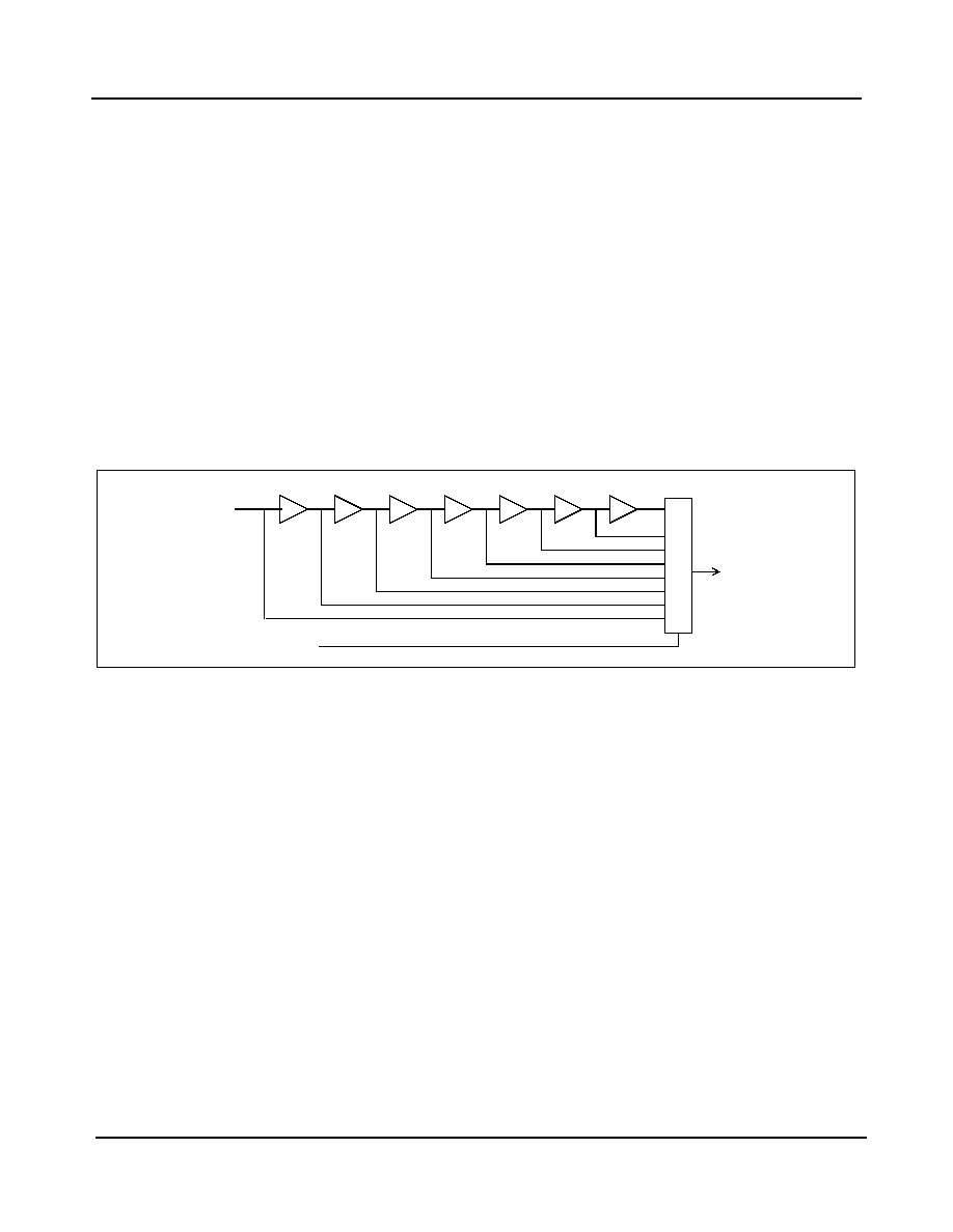
ZL50010
Data Sheet
36
Zarlink Semiconductor Inc.
2.10.2 Reference Select and Frequency Mode Mux Circuits
The DPLL accepts two simultaneous reference inputs and operates on their rising edges. The State Machine output
REF_SELECT chooses either the primary reference (PRI_REF_INT signal) or the secondary reference (SEC_REF
signal) as the REF input to the Skew Control circuit. REF_SELECT also selects the frequency mode input
(FREQ_MOD) to the PLL block from either FREQ_MOD_PRI or FREQ_MOD_SEC. These are two bit wide signals
from the DOM register: FREQ_MOD_PRI corresponds to the FP1-0 bits, FREQ_MOD_SEC corresponds to the
FPS1-0 bits.
2.10.3 Skew Control Circuit
The Skew Control circuit delays the selected reference input with an 8 tap tapped delay line (see Figure 26). The
nominal delay between taps is 1.9 ns. Thus the selected reference can be delayed by 0 to 13.3 ns in steps of 1.9 ns
(0 to 7 steps). The output tap is selected by SKEW_CONTROL which corresponds to the SKC2-0 bits of the DPLL
Output Adjustment (DPOA) register. Skewing the reference will cause the feedback signal in the PLL block
(FEEDBACK in Figure 28 on page 38) to be delayed by the skew amount with respect to the original reference.
This will cause the DPLL output to be delayed by the skew amount. Hence the ST-BUS outputs will be delayed by
the skew amount.
Figure 26 - Skew Control Circuit Diagram
2.10.4 Reference Monitor Circuit
There are two identical Reference Monitor circuits, one for the primary reference PRI_REF_INT and one for the
secondary reference SEC_REF. Each circuit continuously monitors its reference and reports the reference's
validity. The output signals are FAIL_PRI and FAIL_SEC for the primary and secondary monitors respectively. A
logic high on either signal indicates that the corresponding reference has become invalid. The validity criteria
depends on the frequency programmed for the reference. A reference must meet all criteria applicable to its
frequency, which are:
� The "minimum 90 ns" check is performed regardless of the programmed frequency. Both the logic high and
low duration of the reference must be at least 90 ns.
� The "period in specified range" check is performed regardless of the programmed frequency. Each period
must be within a range. For 1.544 MHz and 2.048 MHz, the range is 1-1/4 to 1+1/4 nominal period. For
8 kHz, the range is 1-1/32 to 1+1/32 nominal period.
� If the programmed frequency is 1.544 MHz or 2.048 MHz, the "64 periods in specified range" check will be
performed. The time taken for 64 consecutive cycles must be between 62 and 66 periods of the programmed
frequency.
The FAIL_PRI and FAIL_SEC signals are available at the DHKR register PFD and SFD bits respectively. They are
not affected by the choice of the preferred reference or failure detect mode and will always report the validity of the
primary and secondary references respectively.
MUX
reference
SKEW_CONTROL
delayed
reference
input

ZL50010
Data Sheet
37
Zarlink Semiconductor Inc.
2.10.5 LOS Control Circuit
LOS Control uses the results from the reference monitors to influence the transition of the State Machine. The
outputs of LOS Control are affected by the choice of the failure detect mode (one of autodetect, forced primary, and
forced secondary modes chosen via the DOM register FDM1-0 bits) as shown in Table 15.
Table 15 - LOS Outputs in the Failure Detect Modes
2.10.6 State Machine Circuit
The State Machine manages the reference rearrangement process. The State Machine can be in one of the six
states shown as bubbles in Figure 27. Each bubble shows the state name and state number. Depending on the 3
bit LOS Control output {LOS_PRI, LOS_SEC, REF_SEL} shown in Table 15, the State Machine selects either
PRI_REF_INT or SEC_REF as the current reference. In autodetect mode, the State Machine transitions between
the states during reference rearrangement and switches the PLL circuit between normal and holdover operations.
When the DPLL goes from holdover to normal operation, the State Machine goes through the MTIE PRI or MTIE
SEC state to activate the MTIE circuit. The MTIE circuit prevents any significant phase shift at the PLL output clock
during the reference switch. Note that the PLL is still outputting holdover clock during the MTIE PRI or MTIE SEC
state.
In forced primary mode, the state machine will always stay in "Normal PRI" and never transition to "Holdover PRI".
In forced secondary mode, the state machine will always stay in "Normal SEC" and never transition to "Holdover
SEC".
The DHKR register ST2-0 bits report the state number. In autodetect mode, the ST2-0 bits will follow the state
transitions. In forced primary mode, ST2-0 is always 0. In forced secondary mode, ST2-0 is always 4.
Figure 27 - State Machine Diagram
Failure Detect Mode
LOS_PRI
LOS_SEC
REF_SEL
Autodetect
FAIL_PRI
(from primary
reference monitor)
FAIL_SEC
(from secondary
reference monitor)
REF_SELX
(REFSEL bit in DOM)
(0: primary is preferred reference)
(1: secondary is preferred reference)
Forced Primary
0
1
0
Forced Secondary
1
0
1
Holdover
PRI
Holdover
SEC
MTIE
SEC
Normal
PRI
Normal
SEC
xxx = {LOS_PRI, LOS_SEC, REF_SEL}
1xx or x01
0x0 or 011
0x0
100
1x0
or
x01
or
100 or x01
0x0 or x1x
100 or x01
0x0 or 011
RESET Pin = 0
MTIE
PRI
0x0 or x11
or
x01
0
3
2
7
4
6
011

ZL50010
Data Sheet
38
Zarlink Semiconductor Inc.
2.10.7 Maximum Time Interval Error (MTIE) Circuit
The MTIE circuit prevents any significant change in the DPLL output clock phase during a reference switch. The
input references can have any relationship between their phases. The DPLL output follows the selected input
reference. Thus a switch from one reference to another could cause a large phase jump in the DPLL output if the
MTIE circuit did not exist. The phase jump would be transferred to the ST-BUS outputs. The MTIE circuit works to
preserve the continuity of the DPLL output so that it appears no reference switch had occurred.
The MTIE circuit receives the skewed reference from the Skew Control circuit and delays it. This delayed signal is
used as a virtual reference (REF_VIR in Figure 25 on page 35) to input to the PLL block. Therefore the virtual
reference is a delayed version of the selected reference. During a reference switch, the state machine first changes
the operation of the PLL from normal to holdover. In holdover, the PLL no longer uses the virtual reference signal,
but generates a stable output clock using stored values. When the state machine changes to MTIE PRI or MTIE
SEC, the PLL block remains operating in holdover. The MTIE circuit measures the phase delay between the current
phase (FEEDBACK signal in Figure 25 on page 35) and the phase of the new reference signal (REF_IN in Figure
25). The MTIE circuit stores the measured delay. From now on the MTIE circuit always delays the reference signal
by the stored value to become the virtual reference. The virtual reference is now at the same phase position it
would have been if the reference switch had not taken place. The state machine then returns the PLL to normal
operation.
The PLL now uses the new virtual reference signal. Since no phase step took place at the input of the PLL, no
phase step occurs at the PLL output. In other words, reference switching will not cause a phase change at the PLL
block input, or at the PLL output.
During the measurement process, the new reference is sampled asynchronously with an internal clock. Thus the
delay between the new reference and the old virtual reference has a small measurement error. This measurement
error will cause a small phase change (Time Interval Error) at the PLL output. Even if there is no phase difference
between the primary and secondary references, each time a reference switch is made the delay (phase offset)
between the DPLL input and output will change. The value of the delay is the sum of the measurement errors from
all the reference switches. After many switches, the delay between the selected input reference and the DPLL
output can become unacceptably large. The user should provide MTIE reset (via MRST bit in the DOM register) to
realign the output clock to the nearest edge of the selected input reference. After the realignment, the phase offset
between the input reference and DPLL output is the amount programmed into the DPOA register POS6-0 and
SKC2-0 bits.
2.10.8 Phase-Locked Loop (PLL) Circuit
As shown in Figure 28, the PLL circuit consists of a Phase Detector, Phase Offset Adder, Phase Slope Limiter, Loop
Filter, Digitally Controlled Oscillator, Divider and Frequency Select Mux.
Figure 28 - Block Diagram of the PLL Module
Loop
Filter
DCO
Divider
REF
Phase
Detector
PHASE_OFFSET
Phase
FREQ_MOD
Adder
Offset
Frequency
MCKTDM
FEEDBACK
Phase
Slope
Limiter
MUX
Select
FRAME
C2M
C1M5
HOLDOVER
FREERUN

ZL50010
Data Sheet
39
Zarlink Semiconductor Inc.
Phase Detector - The Phase Detector compares the virtual reference signal from the MTIE circuit (REF_VIR) with
the FEEDBACK signal from the Frequency Select Mux. It provides an error signal corresponding to the phase
difference between the signals' rising edges. This error signal is passed to the Phase Offset Adder.
Phase Offset Adder - The Phase Offset Adder adds the PHASE_OFFSET word (POS6-0 bits of the DPOA register)
to the error signal from the Phase Detector to create the final phase error. This value is passed to the Phase Slope
Limiter. The phase offset word (POS6-0) can be positive or negative. Since the PLL will stabilize to a situation
where the average Phase Offset Adder output is zero, a non-zero phase offset word will result in a static phase
offset between the input and output of the DPLL.
The phase offset word is a 7-bit 2's complement value. If the selected input reference is 8 kHz or 2.048 MHz, the
step size of the static phase offset is 15.2 ns. The static phase offset can be set between -0.96
�
s and +0.97
�
s. If
the selected input reference is 1.544 MHz, the step size is 20.2 ns and the static phase offset can be set between -
1.27
�
s and +1.29
�
s.
The resolution of the Skew Control circuit is 1.9 ns. Its effect is additional to that of the phase offset word. Thus
using the Skew Control bits (SKC2-0 of the DPOA register) together with the phase offset word, users can set a
total static phase offset between -0.96
�
s and +0.99
�
s if the selected input reference is either 8 kHz or 2.048 MHz.
If the selected reference is 1.544 MHz, the total static phase offset can be between -1.27
�
s and +1.30
�
s.
Phase Slope Limiter - The Phase Slope Limiter receives the error signal from the Phase Offset Adder and ensures
that the DPLL output responds to all input transient conditions with an output phase slope below a preset limit. The
limit is based upon telecom standards requirements.
Loop Filter - The Loop Filter is similar to a first order low pass filter with a 1.52 Hz cutoff frequency for all 3
reference frequency selections (8 kHz, 1.544 MHz or 2.048 MHz). This filter defines the jitter transfer characteristic
of the DPLL.
Digitally Controlled Oscillator (DCO) - The DCO generates a high speed digital clock output. The DCO's frequency
is modulated by the frequency offset value from the Loop Filter. The DCO output is the MCKTDM clock in
Figure 25 on page 35 and Figure 28 on page 38. MCKTDM provides timing for the TDM switching function, and
timing for the ST-BUS outputs.
When the State Machine is in the Normal state, the DCO accepts the offset frequency value which represents the
limited and filtered phase error between the input reference and the DCO feedback signal. Based on the offset
value the DCO generates an output clock which is synchronized to the selected input reference.
When the State Machine is in the Holdover state, the DCO uses a frequency offset value which has been stored
32 ms to 64 ms prior to exiting from the Normal state. Thus the DCO is running at the same frequency it was
previously running at when the State Machine was in the Normal state.
When the DPLL is in Freerun mode, the frequency offset is ignored and the DCO is free running at its preset center
frequency.
Divider - The Divider divides down the DCO output frequency. The following signals are generated:
� C2M (a 2.048 MHz clock)
� C1M5 (a 1.544 MHz clock)
� FRAME (an 8 kHz frame pulse)
One of these signals is selected as the PLL feedback reference signal by the Frequency Select Mux circuit. The
clocks have 50% nominal duty cycle. FRAME is a 122 ns wide negative frame pulse. The duty cycle of the clocks
are not affected by the crystal oscillator duty cycle. Since these signals are generated from a common signal inside
the DPLL, the frame pulse and clock outputs are always locked to one another. They are also locked to the selected
input reference when the DPLL is in lock.
Frequency Select Mux - According to the selected input reference of the DPLL, this multiplexer will select the
appropriate divider output C2M, C1M5 or FRAME as the feedback signal to the PLL and MTIE circuits.

ZL50010
Data Sheet
40
Zarlink Semiconductor Inc.
2.11 DPLL Performance
The following are some synchronizer performance indicators and their definitions. The performance of the DPLL is
also indicated.
2.11.1 Intrinsic Jitter
Intrinsic jitter is the jitter produced by a synchronizer and is measured at its output. It is measured by applying a
jitter free reference signal to the input of the device, and measuring its output jitter. Intrinsic jitter may also be
measured when the device is in a non-synchronizing mode, such as free running or holdover, by measuring the
output jitter of the device. Intrinsic jitter is usually measured with various band-limiting filters depending on the
applicable standards.
Intrinsic jitter is applicable only in Master and Freerun modes since in Bypass mode the DPLL is completely
bypassed.
The DPLL's intrinsic jitter is 6.25 ns peak to peak. The intrinsic jitter will be added to the ST-BUS outputs CKo0-2,
FPo0-2, STo0-15 and STOHZ0-15. Since the DPLL master clock (MCKDPLL) comes from the on chip APLL which
is driven by the oscillator, any jitter on the oscillator will be added unattenuated onto the intrinsic jitter.
2.11.2 Jitter Tolerance
Jitter tolerance is a measure of the ability of a PLL to operate properly without cycle slips (i.e., remain in lock and/or
regain lock in the presence of large jitter magnitudes at various jitter frequencies) when jitter is applied to its
reference. The applied jitter magnitude and the jitter frequency depends on the applicable standards.
The DPLL's jitter tolerance meets Telcordia GR-1244-CORE DS1 reference input jitter tolerance requirements.
2.11.3 Jitter Transfer
Jitter transfer or jitter attenuation refers to the magnitude of jitter at the output of a device for a given amount of jitter
at the input of the device. Input jitter is applied at various amplitudes and frequencies, and output jitter is measured
with various filters depending on the applicable standards.
Since intrinsic jitter is always present, jitter attenuation will appear to be lower for small input jitter signals than for
large ones. Consequently, accurate jitter transfer function measurements are usually made with large input jitter
signals (e.g., 75% of the specified maximum jitter tolerance).
The DPLL's jitter transfer characteristic is determined by the internal 1.52 Hz low pass Loop Filter and the Phase
Slope Limiter. The DPLL is a second order, Type 2 PLL. Figure 29 on page 41 shows the DPLL jitter transfer
characteristic over a wide range of frequencies, while Figure 30 on page 41 expands the portion of Figure 29
around the 0 dB jitter transfer region. The jitter transfer function can be described as a low pass filter to 1.52 Hz, -
20 dB/decade, with peaking less then 0.5 dB.
2.11.4 Frequency Accuracy
Frequency accuracy is defined as the absolute tolerance of an output clock when the synchronizer is not locked to
an external reference, but is in a free running mode.
In Freerun mode, the DPLL is not synchronized to any reference. The DPLL provides output clocks and frame
pulses based on the DPLL master clock. The PLL block's DCO circuit ignores its frequency offset input and free
runs at its center frequency. Because of the granularity of the center frequency control value, the DCO free run
frequency is -0.03 ppm off the ideal frequency. The DCO is clocked by the DPLL master clock MCKDPLL. The
APLL generates the DPLL master clock from the oscillator. Thus the DPLL free run accuracy is affected by the
oscillator accuracy. The DPLL free run accuracy is -0.03 ppm plus the accuracy of the oscillator.

ZL50010
Data Sheet
41
Zarlink Semiconductor Inc.
Figure 29 - DPLL Jitter Transfer Function Diagram - Wide Range of Frequencies
Figure 30 - Detailed DPLL Jitter Transfer Function Diagram (Wander Transfer Diagram)

ZL50010
Data Sheet
42
Zarlink Semiconductor Inc.
2.11.5 Holdover Accuracy
Holdover accuracy is defined as the absolute tolerance of an output clock signal, when the synchronizer is not
locked to an external reference signal but is operating using storage techniques.
In the Holdover state, the DPLL is not locked to any reference. The DPLL generates its output clock MCKTDM
using values which were stored while the DPLL was locked to the selected reference in the Normal state. The
values were stored 32 ms to 64 ms prior to exiting from the Normal state.
Two factors affect the holdover accuracy: large jitter on the reference prior to the state change, and the oscillator
frequency drift since the state change. Note that it is the change in the oscillator frequency between the Normal and
Holdover states which affect holdover accuracy, not the absolute frequency of the oscillator.
The DPLL master clock is derived from the oscillator. When the DPLL is in lock, the DPLL output frequency is
exactly the same as that of the input reference. The DPLL will compensate for any changes in the absolute
frequency of the oscillator. In Holdover, the DPLL output frequency is generated using values stored while the DPLL
was in lock. Thus the DPLL can no longer compensate for changes in the oscillator frequency. The holdover
frequency will change if the oscillator frequency has deviated since the DPLL was in lock.
When there was no jitter in the reference, and there is no change in the oscillator frequency, the DPLL holdover
accuracy is within +/-0.07 ppm, which translates into maximum 49 frame slips (6.125 ms) in 24 hours.
Any change in the oscillator frequency since the transition out of the Normal state will change the holdover
frequency. For example, a +/-32 ppm oscillator may have a temperature coefficient of +/-0.1 ppm/
�
C. Thus a 10
�
C
change since the DPLL was last in the Normal state will change the holdover frequency by an additional +/-1 ppm,
which is much greater than the +/-0.07 ppm of the DPLL.
2.11.6 Locking Range
The locking range is the input frequency range over which the DPLL must be able to pull into synchronization and to
maintain the synchronization. The locking range is defined by the Loop Filter circuit and is equal to +/- 298 ppm.
Note that the locking range is related to the oscillator frequency. If the oscillator frequency is -100 ppm, the whole
locking range also shifts by -100 ppm downwards to become -398 ppm to +198 ppm.
2.11.7 Phase Slope
The phase slope, or phase alignment speed, is the rate at which a given signal changes phase with respect to an
ideal signal. The given signal is typically the output signal. The ideal signal is of constant frequency and is nominally
equal to the value of the final output signal or final input signal. Many telecom standards state that the phase slope
may not exceed a certain value, usually 81 ns/1.327 ms (61 ppm). This can be achieved by limiting the phase
detector output to 61 ppm or less.
For the DPLL, the Phase Slope Limiter circuit limits the maximum phase slope to 56 ppm or 7 ns/125
�
s. The phase
slope limit meets Telcordia GR-1244-CORE requirements.
2.11.8 MTIE
MTIE (Maximum Time Interval Error) is the maximum peak to peak delay between a given timing signal and an
ideal timing signal within a particular observation period.
For the DPLL, MTIE is less than 21 ns per reference switch.

ZL50010
Data Sheet
43
Zarlink Semiconductor Inc.
2.11.9 Phase Lock Time
The Phase Lock Time is the time it takes a synchronizer to phase lock to the input signal. Phase lock occurs when
the input and the output signals are not changing in phase with respect to each other (not including jitter).
Lock time is very difficult to determine because it is affected by many factors which include:
i) initial input to output phase difference
ii) initial input to output frequency difference
iii) PLL loop filter
iv) PLL limiter
Although a short phase lock time is desirable, it is not always achievable due to other synchronizer requirements.
For instance, better jitter transfer performance is obtained with a lower frequency loop filter which increases lock
time; and better (smaller) phase slope performance (limiter) will increase lock time.
The DPLL loop filter and limiter have been optimized to meet the Telcordia GR-1244-CORE jitter transfer and
phase alignment speed requirements. If the frequency of the DPLL internal feedback signal is -50 ppm and the
frequency of the input reference is +50 ppm, then the phase lock time is typically 15 seconds. However, in a device
power up situation, phase lock time can be up to 50 seconds. The phase lock time meets Telcordia GR-1244-CORE
Stratum 4E requirements.
2.12 Alignment Between Input and Output Frame Pulses
When the device is in DPLL Master mode, and CKi/FPi is the selected input reference and has no jitter, then the
ST-BUS output frame pulses align very closely to the ST-BUS input frame pulse. See Figure 40 on page 75 for
details. (The alignment shown is for when all bits in the DPOA register are 0.) If the CKi/FPi reference has jitter, the
output frame pulses will still align to the input frame pulse but the offset value is a function of the input jitter.
When the device is in DPLL Master mode, and the selected input reference is not CKi/FPi, then the output frame
pulses have no relationship with respect to the input frame pulse. In this case, the device's output frame pulse(s)
must be used as the frame pulse(s) for the system, which means that the output frame pulse(s) will be supplied as
the input frame pulse to all devices, including the device itself.
When the device is in DPLL Bypass Mode, the output frame pulses align closely to the input frame pulse. See
Figure 40 for details.

ZL50010
Data Sheet
44
Zarlink Semiconductor Inc.
3.0 Oscillator Requirements
In DPLL Master and Freerun modes, the APLL module requires a 20 MHz clock source at the XTALi pin. The
20 MHz clock can be generated by connecting an external crystal oscillator to the XTALi and XTALo pins, or by
connecting an external clock oscillator to the XTALi pin.
If the device is to be used in DPLL Bypass mode only, the 20 MHz clock is not required and the crystal oscillator or
clock oscillator can be omitted. If the crystal oscillator or clock oscillator is omitted, the XTALi pin must be held low
and the XTALo pin must be left unconnected.
3.1 External Crystal Oscillator
A complete external crystal oscillator circuit made up of a crystal, resistor and capacitors is shown in Figure 31.
Figure 31 - Crystal Oscillator Circuit
The accuracy of a crystal oscillator circuit depends on the crystal tolerance as well as the load capacitance
tolerance. Typically, for a 20 MHz crystal specified with a 32 pF load capacitance, each 1 pF change in load
capacitance contributes approximately 9ppm to the frequency deviation. Consequently, capacitor tolerances, and
stray capacitances have a major effect on the accuracy of the oscillator frequency.
The trimmer capacitor may be used to compensate for capacitive effects. If accuracy is not a concern, then the
trimmer may be removed, the 39 pF capacitor may be increased to 56 pF, and a wider tolerance crystal may be
substituted.
The crystal should be a fundamental mode type - not an overtone. The fundamental mode crystal permits a simpler
oscillator circuit with no additional filter components and is less likely to generate spurious responses. The crystal
accuracy only affects the output clock accuracy in the freerun mode. The crystal specification is as follows.
Frequency: 20 MHz
Tolerance: As required
Oscillation Mode: Fundamental
Resonance Mode: Parallel
Load Capacitance: 32 pF
Maximum Series Resistance: 35
Approximate Drive Level: 1 mW
e.g., R1B23B32-20.0 MHz
(20 ppm absolute,
�
6 ppm 0C to 50C, 32 pF, 25
)
XTALo
56 pF
1 M
39 pF
3-50 pF
20 MHz
ZL50010
XTALi
100
1 uH
1 uH inductor: may improve stability and is optional

ZL50010
Data Sheet
45
Zarlink Semiconductor Inc.
3.2 External Clock Oscillator
When an external clock oscillator is used, numerous parameters must be considered. This includes absolute
frequency, frequency change over temperature, output rise and fall times, output levels and duty cycle.
For applications requiring
�
32 ppm clock accuracy, the following clock oscillator module may be used:
FOX F7C-2E3-20.0 MHz
Frequency: 20 MHz
Tolerance: 25 ppm 0C to 70C
Rise & Fall Time: 10 ns (0.33V 2.97V 15 pF)
Duty Cycle: 40% to 60%
The output clock should be connected directly (not AC coupled) to the XTALi input of the device, and the XTALo
output should be left open as shown in Figure 32.
Figure 32 - External Clock Oscillator Circuit
+3.3 V
20 MHz OUT
GND
0.1 uF
+3.3 V
XTALo
XTALi
No Connection
ZL50010

ZL50010
Data Sheet
46
Zarlink Semiconductor Inc.
4.0 Device Reset and Initialization
The RESET pin is used to reset the device. When the pin is low, it synchronously puts the device into its reset state.
It disables the STo0 - 15 outputs, drives the STOHZ 0 - 15 outputs to high, clears the device registers and the
internal counters.
Upon power up, the device should be initialized as follows:
� Set ODE pin to low to disable the STo0-15 output and to drive the STOHZ 0-15 to high.
� Set the TRST pin to low to disable the JTAG TAP controller.
� Reset the device by pulsing the RESET pin to low for longer than 1 ms.
� After releasing the RESET pin from low to high, wait for 600
�
s for the APLL module and the crystal
oscillator to be stabilized before starting the first microprocessor port access cycle.
� Program the register to define the frequency of the CKi input.
� Wait for 600
�
s for the APLL module to be stabilized before starting the next microprocessor port access
cycle.
� Configure the DPLL. After a device reset, the DPLL defaults are: Master mode, failure detect mode is
Autodetect, primary reference is PRI_REF at 8 kHz, SEC_REF frequency is 8 kHz, preferred reference is
the primary reference, polarities of PRI_REF and SEC_REF are not inverted.
� If DPLL Master mode is selected, wait 50 seconds for the DPLL to synchronize to the reference.
� Use the memory block programming mode to initialize the connection memory.
� Release the ODE pin to high after the connection memory is programmed such that bus contention will not
occur at the serial stream outputs STo0-15.
5.0 JTAG Support
The ZL50010 JTAG interface conforms to the Boundary-Scan IEEE1149.1 standard. The operation of the
boundary-scan circuitry is controlled by an external Test Access Port (TAP) Controller.
5.1 Test Access Port (TAP)
The Test Access Port (TAP) accesses the ZL50010 test functions. It consists of 3 input pins and 1 output pin as
follows:
� Test Clock Input (TCK) - TCK provides the clock for the test logic. The TCK does not interfere with any on-
chip clock and thus remains independent in the functional mode. The TCK permits shifting of test data into or
out of the Boundary-Scan register cells concurrently with the operation of the device and without interfering
with the on-chip logic.
� Test Mode Select Input (TMS) - The TAP Controller uses the logic signals received at the TMS input to
control test operations. The TMS signals are sampled at the rising edge of the TCK pulse. This pin is
internally pulled to Vdd when it is not driven from an external source.
� Test Data Input (TDi) - Serial input data applied to this port is fed either into the instruction register or into a
test data register, depending on the sequence previously applied to the TMS input. Both registers are
described in a subsequent section. The received input data is sampled at the rising edge of TCK pulses.
This pin is internally pulled to Vdd when it is not driven from an external source.
� Test Data Output (TDo) - Depending on the sequence previously applied to the TMS input, the contents of
either the instruction register or data register are serially shifted out towards the TDO. The data out of the
TDO is clocked on the falling edge of the TCK pulses. When no data is shifted through the boundary scan
cells, the TDO driver is set to a high impedance state.
� Test Reset (TRST) - Resets the JTAG scan structure. This pin is internally pulled to Vdd when it is not driven
from an external source.

ZL50010
Data Sheet
47
Zarlink Semiconductor Inc.
5.2 Instruction Register
The ZL50010 uses the public instructions defined in the IEEE 1149.1 standard. The JTAG Interface contains a four-
bit instruction register. Instructions are serially loaded into the instruction register from the TDI when the TAP
Controller is in its shifted-IR state. These instructions are subsequently decoded to achieve two basic functions: to
select the test data register that may operate while the instruction is current and to define the serial test data
register path that is used to shift data between TDI and TDO during data register scanning.
5.3 Test Data Register
As specified in IEEE 1149.1, the ZL50010 JTAG Interface contains three test data registers:
� The Boundary-Scan Register - The Boundary-Scan register consists of a series of Boundary-Scan cells
arranged to form a scan path around the boundary of the ZL50010 core logic.
� The Bypass Register - The Bypass register is a single stage shift register that provides a one-bit path from
TDI to its TDO.
� The Device Identification Register - The JTAG device ID for the ZL50010 is 0C35A14B
H
.
Version<31:28>: 0000
Part No. <27:12>: 1100 0011 0101 1010
Manufacturer ID<11:1>: 0001 0100 101
LSB<0>: 1
5.4 BSDL
A BSDL (Boundary Scan Description Language) file is available from Zarlink Semiconductor to aid in the use of the
IEEE 1149 test interface.

ZL50010
Data Sheet
48
Zarlink Semiconductor Inc.
6.0 Register Address Mapping
External
Address
A11 - A0
CPU
Access
Register
000
H
R/W
Control Register, CR
001
H
R/W
Internal Mode Selection, IMS
010
H
R/W
BER Start Receive Register, BSRR
011
H
R/W
BER Length Register, BLR
012
H
Read Only
BER Count Register, BCR
030
H
R/W
DPLL Operation Mode, DOM
031
H
R/W
DPLL Output Adjustment, DPOA
032
H
Read Only
DPLL House Keeping Register, DHKR
100
H
R/W
Stream0 Input Control Register, SICR0
101
H
R/W
Stream0 Input Delay Register, SIDR0
102
H
R/W
Stream1 Input Control Register, SICR1
103
H
R/W
Stream1 Input Delay Register, SIDR1
104
H
R/W
Stream2 Input Control Register, SICR2
105
H
R/W
Stream2 Input Delay Register, SIDR2
106
H
R/W
Stream3 Input Control Register, SICR3
107
H
R/W
Stream3 Input Delay Register, SIDR3
108
H
R/W
Stream4 Input Control Register, SICR4
109
H
R/W
Stream4 Input Delay Register, SIDR4
10A
H
R/W
Stream5 Input Control Register, SICR5
10B
H
R/W
Stream5 Input Delay Register, SIDR5
10C
H
R/W
Stream6 Input Control Register, SICR6
10D
H
R/W
Stream6 Input Delay Register, SIDR6
10E
H
R/W
Stream7 Input Control Register, SICR7
10F
H
R/W
Stream7 Input Delay Register, SIDR7
110
H
R/W
Stream8 Input Control Register, SICR8
111
H
R/W
Stream8 Input Delay Register, SIDR8
112
H
R/W
Stream9 Input Control Register, SICR9
113
H
R/W
Stream9 Input Delay Register, SIDR9
114
H
R/W
Stream10 Input Control Register, SICR10
115
H
R/W
Stream10 Input Delay Register, SIDR10
116
H
R/W
Stream11 Input Control Register, SICR11
117
H
R/W
Stream11 Input Delay Register, SIDR11
118
H
R/W
Stream12 Input Control Register, SICR12
119
H
R/W
Stream12 Input Delay Register, SIDR12
11A
H
R/W
Stream13 Input Control Register, SICR13
11B
H
R/W
Stream13 Input Delay Register, SIDR13
11C
H
R/W
Stream14 Input Control Register, SICR14

ZL50010
Data Sheet
49
Zarlink Semiconductor Inc.
Table 16 - Address Map for Device Specific Registers
11D
H
R/W
Stream14 Input Delay Register, SIDR14
11E
H
R/W
Stream15 Input Control Register, SICR15
11F
H
R/W
Stream15 Input Delay Register, SIDR15
200
H
R/W
Stream0 Output Control Register, SOCR0
201
H
R/W
Stream0 Output Delay Register, SOOR0
202
H
R/W
Stream1 Output Control Register, SOCR1
203
H
R/W
Stream1 Output Delay Register, SOOR1
204
H
R/W
Stream2 Output Control Register, SOCR2
205
H
R/W
Stream2 Output Delay Register, SOOR2
206
H
R/W
Stream3 Output Control Register, SOCR3
207
H
R/W
Stream3 Output Delay Register, SOOR3
208
H
R/W
Stream4 Output Control Register, SOCR4
209
H
R/W
Stream4 Output Delay Register, SOOR4
20A
H
R/W
Stream5 Output Control Register, SOCR5
20B
H
R/W
Stream5 Output Delay Register, SOOR5
20C
H
R/W
Stream6 Output Control Register, SOCR6
20D
H
R/W
Stream6 Output Delay Register, SOOR6
20E
H
R/W
Stream7 Output Control Register, SOCR7
20F
H
R/W
Stream7 Output Delay Register, SOOR7
210
H
R/W
Stream8 Output Control Register, SOCR8
211
H
R/W
Stream8 Output Delay Register, SOOR8
212
H
R/W
Stream9 Output Control Register, SOCR9
213
H
R/W
Stream9 Output Delay Register, SOOR9
214
H
R/W
Stream10 Output Control Register, SOCR10
215
H
R/W
Stream10 Output Delay Register, SOOR10
216
H
R/W
Stream11 Output Control Register, SOCR11
217
H
R/W
Stream11 Output Delay Register, SOOR11
218
H
R/W
Stream12 Output Control Register, SOCR12
219
H
R/W
Stream12 Output Delay Register, SOOR12
21A
H
R/W
Stream13 Output Control Register, SOCR13
21B
H
R/W
Stream13 Output Delay Register, SOOR13
21C
H
R/W
Stream14 Output Control Register, SOCR14
21D
H
R/W
Stream14 Output Delay Register, SOOR14
21E
H
R/W
Stream15 Output Control Register, SOCR15
21F
H
R/W
Stream15 Output Delay Register, SOOR15
External
Address
A11 - A0
CPU
Access
Register

ZL50010
Data Sheet
50
Zarlink Semiconductor Inc.
7.0 Detail Register description
Bit
Name
Description
15
Unused
Reserved. In normal functional mode, these bits MUST be set to zero.
14
SLV
DPLL Bypass Mode Enable.
When this bit is zero, the DPLL is in Master or Freerun mode. When this bit is high, the
DPLL is in Bypass mode.
13
FBDEN
Frame Boundary Determination Disable.
When this bit is low, the long term frame boundary determination mode is disabled.
When it is high, the determination mode is enabled.
Set this bit from low to high after waiting for 600
�
s upon device power up.
12 - 10
CKIN2-0
Input ST Bus Clock (CKi) and Frame Pulse (FPi) Selection.
9
CKFP2
Output ST Bus clock CKo2 and frame pulse FPo2 Selection.
When this bit is low, CKo2 is 32.768 MHz clock and FPo2 is 30 ns wide frame pulse
When this bit is high, CKo2 is 16.384 MHz clock and FPo2 is 61 ns wide frame pulse
8
CKFP1
Output ST Bus clock CKo1 and frame pulse FPo1 Selection.
When this bit is low, CKo1 is 16.384 MHz clock and FPo1 is 61 ns wide frame pulse
When this bit is high, CKo1 is 8.192 MHz clock and FPo1 is 122 ns wide frame pulse
7
CKFP0
Output ST Bus clock CKo0 and frame pulse FPo0 Selection.
When this bit is low, CKo0 is 4.096 MHz clock and FPo0 is 244 ns wide frame pulse
When this bit is high, CKo0 is 8.192 MHz clock and FPo0 is 122 ns wide frame pulse
6
CBER
Bit Error Rate Counter Clear: When this bit is high, it resets the internal bit error
counter and the content of the bit error count register (BCR) to zero. Upon completion of
the reset, set this bit to zero.
5
SBER
Bit Error Rate Test Start: When this bit is high, it enables the BER transmitter and
receiver; starts the bit error rate test. The bit error test result is kept in the bit error count
(BCR) register. Upon the completion of the BER test, set this bit to zero.
4
MBPE
Memory Block Programming Enable: When this bit is high, the connection memory
block programming mode is enabled to program Bit 0 to Bit 2 of the connection memory.
When it is low, the memory block programming mode is disabled.
Table 17 - Control Register (CR) Bits
External Read/Write Address: 000
H
Reset Value: 0000
H
15
14
13
12
11
10
9
8
7
6
5
4
3
2
1
0
0
SLV
FBD
EN
CKIN
2
CKIN
1
CKIN
0
CKFP
2
CKFP
1
CKFP
0
CBER
SBER
MBPE
OSB
MS2
MS1
MS0
CKIN2 - 0
FPi Low Cycle
CKi
000
61 ns
16.384 MHz
001
122 ns
8.192 MHz
010
244 ns
4.096 MHz
011 - 111
Reserved

ZL50010
Data Sheet
51
Zarlink Semiconductor Inc.
3
OSB
Output Stand By Bit: This bit enables the STo0 - 15 and the STOHZ 0 -15 serial outputs.
The
following table describes the HiZ control of the serial data outputs:
2 - 0
MS2-0
Memory Select Bit. These bits are used to select connection memory or data memory:
Bit
Name
Description
Table 17 - Control Register (CR) Bits (continued)
External Read/Write Address: 000
H
Reset Value: 0000
H
15
14
13
12
11
10
9
8
7
6
5
4
3
2
1
0
0
SLV
FBD
EN
CKIN
2
CKIN
1
CKIN
0
CKFP
2
CKFP
1
CKFP
0
CBER
SBER
MBPE
OSB
MS2
MS1
MS0
RESET
Pin
ODE
Pin
OSB
Bit
STo0-15
STOHZ 0-15
0
X
X
HiZ
Driven High
1
0
X
HiZ
Driven High
1
1
0
HiZ
Driven High
1
1
1
Active
Active
MS2 - 0
Memory Selection
000
Connection Memory Read/Write
001
Data memory Read
010 - 111
Reserved

ZL50010
Data Sheet
52
Zarlink Semiconductor Inc.
Bit
Name
Description
15 - 12
Unused
Reserved. In normal functional mode, these bits MUST be set to zero.
11
CKINP
ST Bus Clock Input (CKi) Polarity
When this bit is low, the CKi falling edge aligns with the frame boundary.
When this bit is high, the CKi rising edge aligns with the frame boundary.
10
FPINP
Frame Pulse Input (FPi) Polarity
When this bit is low, the input frame pulse FPi should have the negative frame pulse
format. When this bit is high, the input frame pulse FPi should have the positive frame
pulse format.
9
CK2P
ST Bus Clock Output (CKo2) Polarity
When this bit is low, the output clock CKo2 falling edge aligns with the frame
boundary. When this bit is high, the output clock CKo2 rising edge aligns with the
frame boundary.
8
FP2P
Frame Pulse Output (FPo2) Polarity
When this bit is low, the output frame pulse FPo2 has the negative frame pulse format.
When this bit is high, the output frame pulse FPo2 has the positive frame pulse format.
7
CK1P
ST Bus Clock Output (CKo1) Polarity
When this bit is low, the output clock CKo1 falling edge aligns with the frame bound-
ary. When this bit is high, the output clock CKo1 rising edge aligns with the frame
boundary.
6
FP1P
Frame Pulse Output (FPo1) Polarity
When this bit is low, the output frame pulse FPo1 has the negative frame pulse format.
When this bit is high, the output frame pulse FPo1 has the positive frame pulse format.
5
CK0P
ST Bus Clock Output (CKo0) Polarity
When this bit is low, the output clock CKo0 falling edge aligns with the frame
boundary. When this bit is high, the output clock CKo0 rising edge aligns with the
frame boundary.
4
FP0P
Frame Pulse Output (FPo0) Polarity
When this bit is low, the output frame pulse FPo0 has the negative frame pulse format.
When this bit is high, the output frame pulse FPo0 has the positive frame pulse format.
3 - 1
BPD2 - 0
Block Programming Data: These bits refer to the value to be loaded into the
connection memory. Whenever the memory block programming feature is activated.
After the MBPE bit in the control register is set to high and the MBPS bit is set to high,
the contents of the bits BPD0 to BPD2 are loaded into Bit 0 to Bit 2 of the connection
memory. Bit 3 to Bit 11 of the connection memory are zeroed.
Table 18 - Internal Mode Selection (IMS) Register Bits
External Read/Write Address: 001
H
Reset Value: 0000
H
15
14
13
12
11
10
9
8
7
6
5
4
3
2
1
0
0
0
0
0
CKINP
FPINP
CK2P
FP2P
CK1P
FP1P
CK0P
FP0P
BPD
2
BPD
1
BPD
0
MBPS

ZL50010
Data Sheet
53
Zarlink Semiconductor Inc.
Table 19 - BER Start Receiving Register (BSRR) Bits
0
MBPS
Memory Block Programming Start: A zero to one transition of this bit starts the
memory block programming function. The MBPS, BPD0 to BPD2 bits in this register
must be defined in the same write operation. Once the MBPE bit in the control register
is set to high, the device requires 50
�
s to complete the block programming. After the
programming function has finished, the MBPS bit returns to low indicating the opera-
tion is completed. When the MBPS is high, the MBPS or MBPE can be set to low to
abort the programming operation.
To ensure proper block programming operation, when MBPS is high the BPD0 to
BPD2 bits in this register must not be changed.
Whenever the microprocessor writes a one to the MBPS bit, the block programming
function is started, the user must maintain the same logical value to the other bits in
this register to avoid any change in the device setting.
Bit
Name
Description
15 - 13
8 - 7
Unused
Reserved. In normal functional mode, these bits MUST be set to zero.
12 - 9
BRSA3 - 0
BER Receive Stream Address Bits: The binary value of these bits refers to the input
stream which receives the BER data.
6 - 0
BRCA6 - 0
BER Receive Channel Address Bits: The binary value of these bits refers to the
input channel in which the BER data starts to be compared.
Bit
Name
Description
Table 18 - Internal Mode Selection (IMS) Register Bits (continued)
External Read/Write Address: 001
H
Reset Value: 0000
H
15
14
13
12
11
10
9
8
7
6
5
4
3
2
1
0
0
0
0
0
CKINP
FPINP
CK2P
FP2P
CK1P
FP1P
CK0P
FP0P
BPD
2
BPD
1
BPD
0
MBPS
External Read/Write Address: 010
H
Reset Value: 0000
H
15
14
13
12
11
10
9
8
7
6
5
4
3
2
1
0
0
0
0
BR
SA3
BR
SA2
BR
SA1
BR
SA0
0
0
BR
CA6
BR
CA5
BR
CA4
BR
CA3
BR
CA2
BR
CA1
BR
CA0

ZL50010
Data Sheet
54
Zarlink Semiconductor Inc.
Table 20 - BER Length Register (BLR) Bits
Table 21 - BER Count Register (BCR) Bits
Bit
Name
Description
15 - 8
Unused
Reserved. In normal functional mode, these bits MUST be set to zero.
7 - 0
BL7 - 0
BER Length Bits: The binary value of these bits refers to the number of channels.
The maximum numbers of BER channels are 32, 64 and 128 for the data rate of
2.048 Mbps, 4.096 Mbps and 8.192 Mbps modes respectively. The minimum number
of BER channel is 1. If these bits are set to zero, no BER test will be performed.
Bit
Name
Description
15 - 0
BC15 - 0
BER Count Bits: The binary value of these bits refers to the bit error counts. When it
reaches its maximum value of Hex FFFF, the value will not be changed any more.
External
Read/Write Address: 011
H
Reset Value: 0000H
15
14
13
12
11
10
9
8
7
6
5
4
3
2
1
0
0
0
0
0
0
0
0
0
BL7
BL6
BL5
BL4
BL3
BL2
BL1
BL0
External
Read Address: 012
H
Reset Value: 0000H
15
14
13
12
11
10
9
8
7
6
5
4
3
2
1
0
BC
15
BC
14
BC
13
BC
12
BC
11
BC
10
BC
9
BC
8
BC
7
BC
6
BC
5
BC
4
BC
3
BC
2
BC
1
BC
0

ZL50010
Data Sheet
55
Zarlink Semiconductor Inc.
Bit
Name
Description
15 - 12
Unused
Reserved. In normal functional mode, these bits MUST be set to zero.
11
MRST
MTIE Reset Bit: When MRST is low, the DPLL MTIE circuit is functional. When MRST
is high, the MTIE circuit will be reset - the DPLL output will align with the nearest edge
of the selected reference. (Note: After the realignment, the phase offset between the
input reference and DPLL output is the amount programmed into the DPOA register.)
10 - 9
FDM1 - 0
Failure Detect Mode Bits: These two bits are used to choose among one of three
Failure Detection modes.
8
SINV
SEC_REF Input Inversion: When this bit is low, the SEC_REF input will not be
inverted. When this bit is high, the SEC_REF input will be inverted.
7
PINV
PRI_REF Input Inversion: When this bit is low, the PRI_REF input will not be
inverted. When this bit is high, the PRI_REF input will be inverted.
6 - 5
FS1 - FS0
SEC_REF Frequency Selection Bits: These bits are used to specify the nominal
clock frequency of the SEC_REF input.
Table 22 - DPLL Operation Mode (DOM) Register Bits
External Read/Write Address: 030
H
Reset Value: 0000
H
15
14
13
12
11
10
9
8
7
6
5
4
3
2
1
0
0
0
0
0
MRST
FDM1
FDM0
SINV
PINV
FS1
FS0
FP1
FP0
REF
SEL
P_REF
SEL
FREE
RUN
FDM1
FDM0
Failure Detection Mode
0
0
Autodetect - Automatic Reference Re-arrangement based on
reference monitor results and choice of preferred reference
0
1
Reserved
1
0
Forced Primary - The DPLL is forced to use primary reference
only
1
1
Forced Secondary - The DPLL is forced to use secondary
reference only
FS1
FS0
Secondary Reference
0
0
8 kHz
0
1
1.544 MHz
1
0
2.048 MHz
1
1
Reserved

ZL50010
Data Sheet
56
Zarlink Semiconductor Inc.
4 - 3
FP1 - FP0
PRI_REF Frequency Selection Bits: These bits are used to specify the nominal
clock frequency of the PRI_REF input.
When the P_REFSEL bit is high to select the internal 8 kHz signal (derived from the
FPi and CKi inputs) as primary reference, these bits must be set to 00.
2
REFSEL
Preferred Reference Selection Bit: When this bit is low, the preferred reference is
the primary reference selected via the P_REFSEL bit (PRI_REF or internal 8 kHz from
FPi and CKi). When this bit is high, the preferred reference is the secondary reference
(SEC_REF).
1
P_REFSEL
Primary Reference Source Selection Bit: This bit is used to select the primary
reference input to the DPLL from between 2 sources. When this bit is low, the primary
reference is from the PRI_REF pin. When this bit is high, the primary reference is from
the internal 8 kHz generated from the FPi and CKi inputs. When this bit is high, the
FP1-0 bits must be set to 00.
If the internal 8 kHz signal is selected as the primary reference, the user must ensure
that the FPi and CKi input signals will be re-applied after the internal 8 kHz signal is
lost (or failed). If FPi or CKi is not presented to the device, the device cannot accept
STi0-15 input data.
0
FREERUN
Freerun Control Bit: When this bit is low and bit 14 of the Control Register is low, the
DPLL is in Master mode. When this bit is high and bit 14 of the Control Register is low,
the DPLL is in Freerun mode. This bit has no effect when bit 14 of the Control Register
is high.
Bit
Name
Description
Table 22 - DPLL Operation Mode (DOM) Register Bits (continued)
External Read/Write Address: 030
H
Reset Value: 0000
H
15
14
13
12
11
10
9
8
7
6
5
4
3
2
1
0
0
0
0
0
MRST
FDM1
FDM0
SINV
PINV
FS1
FS0
FP1
FP0
REF
SEL
P_REF
SEL
FREE
RUN
FP1
FP0
Primary Reference
0
0
8 kHz (PRI_REF or CKi/FPi)
0
1
1.544 MHz
1
0
2.048 MHz
1
1
Reserved

ZL50010
Data Sheet
57
Zarlink Semiconductor Inc.
Table 23 - DPLL Output Adjustment (DPOA) Register Bits
Table 24 - DPLL House Keeping (DHKR) Register Bits
Bit
Name
Description
15 - 10
Unused
Reserved. In normal functional mode, these bits MUST be set to zero.
9 - 3
POS6 - 0
Phase Offset Bits: These 7 bits form the 2's complement phase offset word which
controls the DPLL output phase offset. The DPLL output is advanced (leads the refer-
ence) if the word is positive. The DPLL output is delayed (lags the reference) if the
word is negative. The net effect is that the ST-BUS outputs will be advanced or
delayed by the programmed amount.
The offset is in step of 15.2 ns if the input reference is 8 kHz or 2.048 MHz. The offset
is in step of 20.2 ns if the input reference is 1.544 MHz. These bits have no effect in
Freerun or Bypass mode.
2 - 0
SKC2 - 0
Skew Control Bits: These 3 bits control the delay of the DPLL outputs from 0 to
13.3 ns in steps of 1.9 ns. The net effect is that the ST-BUS outputs will be delayed by
the programmed amount. These bits have no effect in Freerun or Bypass mode.
Bit
Name
Description
15 - 6
Unused
Reserved. In normal functional mode, these bits MUST be set to zero.
5
SFD
Secondary Fail Detection Bit (Read only bit): This bit reports the validity of the
SEC_REF signal. When the secondary reference fails, this bit is set to high.
4
PFD
Primary Fail Detection Bit (Read only bit): This bit reports the validity of the primary
reference signal selected by the P_REFSEL bit in the DOM register. When the
selected primary reference fails, this bit is set to high.
3
LMT
DPLL LIMIT Bit (Read only bit): This bit indicates that the Phase Slope Limiter is
limiting the phase difference between the input reference and the feedback reference.
2 - 0
ST2- 0
DPLL State Bits (Read only bit): These bits report the state of the DPLL state
machine. The state numbers are shown in the bubbles in Figure 27 on page 37.
External Read/Write Address: 031
H
Reset Value: 0000
H
15
14
13
12
11
10
9
8
7
6
5
4
3
2
1
0
0
0
0
0
0
0
POS6
POS5
POS4
POS3
POS2
POS1
POS0
SKC2
SKC1
SKC0
External Read Address: 032
H
Reset Value: 0000
H
15
14
13
12
11
10
9
8
7
6
5
4
3
2
1
0
0
0
0
0
0
0
0
0
0
0
SFD
PFD
LMT
ST2
ST1
ST0

ZL50010
Data Sheet
58
Zarlink Semiconductor Inc.
Bit
Name
Description
15 - 9
Unused
Reserved. In normal functional mode, these bits MUST be set to zero.
8
STIN#QEN3
Quadrant Frame 3 Enable. When this bit is low, the device is in normal
operation mode. When this bit is high, the LSB of every channel in this
quadrant frame is replaced by "1". This quadrant frame is defined as Ch24 to
31, Ch48 to 63 and Ch96 to 127 for the 2.048 Mbps, 4.096 Mbps and
8.192 Mbps mode respectively.
7
STIN#QEN2
Quadrant Frame 2 Enable. When this bit is low, the device is in normal
operation mode. When this bit is high, the LSB of every channel in this
quadrant frame is replaced by "1". This quadrant frame is defined as Ch16 to
23, Ch32 to 47 and Ch64 to 95 for the 2.048 Mbps, 4.096 Mbps and
8.192 Mbps mode respectively.
6
STIN#QEN1
Quadrant Frame 1 Enable. When this bit is low, the device is in normal
operation mode. When this bit is high, the LSB of every channel in this
quadrant frame is replaced by "1". This quadrant frame is defined as Ch8 to 15,
Ch16 to 31 and Ch32 to 63 for the 2.048 Mbps, 4.096 Mbps and 8.192 Mbps
mode respectively.
5
STIN#QEN0
Quadrant Frame 0 Enable. When this bit is low, the device is in normal
operation mode. When this bit is high, the LSB of every channel in this
quadrant frame is replaced by "1". This quadrant frame is defined as Ch0 to 7,
Ch0 to 15 and Ch0 to 31 for 2.048 Mbps, the 4.096 Mbps and 8.192 Mbps
mode respectively.
Table 25 - Stream Input Control Register 0 to 7 (SICR0 to SICR7)
External Read/Write Address: 100
H
, 102
H
, 104
H
, 106
H
, 108
H
, 10A
H
, 10C
H
, 10E
H
,
Reset Value: 0000
H
15
14
13
12
11
10
9
8
7
6
5
4
3
2
1
0
SICR0
0
0
0
0
0
0
0
STIN0
QEN3
STIN0
QEN2
STIN0
QEN1
STIN0
QEN0
STIN0
SMP1
STIN0
SMP0
STIN0
DR2
STIN0
DR1
STIN0
DR0
SICR1
0
0
0
0
0
0
0
STIN1
QEN3
STIN1
QEN2
STIN1
QEN1
STIN1
QEN0
STIN1
SMP1
STIN1
SMP0
STIN1
DR2
STIN1
DR1
STIN1
DR0
SICR2
0
0
0
0
0
0
0
STIN2
QEN3
STIN2
QEN2
STIN2
QEN1
STIN2
QEN0
STIN2
SMP1
STIN2
SMP0
STIN2
DR2
STIN2
DR1
STIN2
DR0
SICR3
0
0
0
0
0
0
0
STIN3
QEN3
STIN3
QEN2
STIN3
QEN1
STIN3
QEN0
STIN3
SMP1
STIN3
SMP0
STIN3
DR2
STIN3
DR1
STIN3
DR0
SICR4
0
0
0
0
0
0
0
STIN4
QEN3
STIN4
QEN2
STIN4
QEN1
STIN4
QEN0
STIN4
SMP1
STIN4
SMP0
STIN4
DR2
STIN4
DR1
STIN4
DR0
SICR5
0
0
0
0
0
0
0
STIN5
QEN3
STIN5
QEN2
STIN5
QEN1
STIN5
QEN0
STIN5
SMP1
STIN5
SMP0
STIN5
DR2
STIN5
DR1
STIN5
DR0
SICR6
0
0
0
0
0
0
0
STIN6
QEN3
STIN6
QEN2
STIN6
QEN1
STIN6
QEN0
STIN6
SMP1
STIN6
SMP0
STIN6
DR2
STIN6
DR1
STIN6
DR0
SICR7
0
0
0
0
0
0
0
STIN7
QEN3
STIN7
QEN2
STIN7
QEN1
STIN7
QEN0
STIN7
SMP1
STIN7
SMP0
STIN7
DR2
STIN7
DR1
STIN7
DR0

ZL50010
Data Sheet
59
Zarlink Semiconductor Inc.
4 - 3
STIN#SMP1 - 0
Input Data Sampling Point Selection Bits
:
2 - 0
STIN#DR2 - 0
Input Data Rate Selection Bits:
Note: # denotes input stream from 0 to 7
Bit
Name
Description
Table 25 - Stream Input Control Register 0 to 7 (SICR0 to SICR7) (continued)
External Read/Write Address: 100
H
, 102
H
, 104
H
, 106
H
, 108
H
, 10A
H
, 10C
H
, 10E
H
,
Reset Value: 0000
H
15
14
13
12
11
10
9
8
7
6
5
4
3
2
1
0
SICR0
0
0
0
0
0
0
0
STIN0
QEN3
STIN0
QEN2
STIN0
QEN1
STIN0
QEN0
STIN0
SMP1
STIN0
SMP0
STIN0
DR2
STIN0
DR1
STIN0
DR0
SICR1
0
0
0
0
0
0
0
STIN1
QEN3
STIN1
QEN2
STIN1
QEN1
STIN1
QEN0
STIN1
SMP1
STIN1
SMP0
STIN1
DR2
STIN1
DR1
STIN1
DR0
SICR2
0
0
0
0
0
0
0
STIN2
QEN3
STIN2
QEN2
STIN2
QEN1
STIN2
QEN0
STIN2
SMP1
STIN2
SMP0
STIN2
DR2
STIN2
DR1
STIN2
DR0
SICR3
0
0
0
0
0
0
0
STIN3
QEN3
STIN3
QEN2
STIN3
QEN1
STIN3
QEN0
STIN3
SMP1
STIN3
SMP0
STIN3
DR2
STIN3
DR1
STIN3
DR0
SICR4
0
0
0
0
0
0
0
STIN4
QEN3
STIN4
QEN2
STIN4
QEN1
STIN4
QEN0
STIN4
SMP1
STIN4
SMP0
STIN4
DR2
STIN4
DR1
STIN4
DR0
SICR5
0
0
0
0
0
0
0
STIN5
QEN3
STIN5
QEN2
STIN5
QEN1
STIN5
QEN0
STIN5
SMP1
STIN5
SMP0
STIN5
DR2
STIN5
DR1
STIN5
DR0
SICR6
0
0
0
0
0
0
0
STIN6
QEN3
STIN6
QEN2
STIN6
QEN1
STIN6
QEN0
STIN6
SMP1
STIN6
SMP0
STIN6
DR2
STIN6
DR1
STIN6
DR0
SICR7
0
0
0
0
0
0
0
STIN7
QEN3
STIN7
QEN2
STIN7
QEN1
STIN7
QEN0
STIN7
SMP1
STIN7
SMP0
STIN7
DR2
STIN7
DR1
STIN7
DR0
STIN#SMP1-0
Sampling Point
00
3/4 point
01
4/4 point
10
1/4 point
11
2/4 point
STIN#DR2-0
Data Rate
000
Disabled - External pull-up or pull-down
is required for ST-BUS input
001
2.048 Mbps
010
4.096 Mbps
011
8.192 Mbps
100 - 111
Reserved

ZL50010
Data Sheet
60
Zarlink Semiconductor Inc.
Bit
Name
Description
15 - 9
Unused
Reserved. In normal functional mode, these bits MUST be set to zero.
8
STIN#QEN3
Quadrant Frame 3 Enable. When this bit is low, the device is in normal
operation mode. When this bit is high, the LSB of every channel in this
quadrant frame is replaced by "1". This quadrant frame is defined as Ch24 to
31, Ch48 to 63 and Ch96 to 127 for the 2.048 Mbps, 4.096 Mbps and
8.192 Mbps mode respectively.
7
STIN#QEN2
Quadrant Frame 2 Enable. When this bit is low, the device is in normal
operation mode. When this bit is high, the LSB of every channel in this
quadrant frame is replaced by "1". This quadrant frame is defined as Ch16 to
23, Ch32 to 47 and Ch64 to 95 for the 2.048 Mbps, 4.096 Mbps and
8.192 Mbps mode respectively.
6
STIN#QEN1
Quadrant Frame 1 Enable. When this bit is low, the device is in normal
operation mode. When this bit is high, the LSB of every channel in this
quadrant frame is replaced by "1". This quadrant frame is defined as Ch8 to 15,
Ch16 to 31 and Ch32 to 63 for the 2.048 Mbps, 4.096 Mbps and 8.192 Mbps
mode respectively.
5
STIN#QEN0
Quadrant Frame 0 Enable. When this bit is low, the device is in normal
operation mode. When this bit is high, the LSB of every channel in this
quadrant frame is replaced by "1". This quadrant frame is defined as Ch0 to 7,
Ch0 to 15 and Ch0 to 31 for 2.048 Mbps, the 4.096 Mbps and 8.192 Mbps
mode respectively.
Table 26 - Stream Input Control Register 8 to 15 (SICR8 to SICR15)
External Read/Write Address: 110
H
, 112
H
, 114
H
, 116
H
, 118
H
, 11A
H
, 11C
H
, 11E
H
,
Reset Value: 0000
H
15
14
13
12
11
10
9
8
7
6
5
4
3
2
1
0
SICR8
0
0
0
0
0
0
0
STIN8
QEN3
STIN8
QEN2
STIN8
QEN1
STIN8
QEN0
STIN8
SMP1
STIN8
SMP0
STIN8
DR2
STIN8
DR1
STIN8
DR0
SICR9
0
0
0
0
0
0
0
STIN9
QEN3
STIN9
QEN2
STIN9
QEN1
STIN9
QEN0
STIN9
SMP1
STIN9
SMP0
STIN9
DR2
STIN9
DR1
STIN9
DR0
SICR10
0
0
0
0
0
0
0
STIN10
QEN3
STIN10
QEN2
STIN10
QEN1
STIN10
QEN0
STIN10
SMP1
STIN10
SMP0
STIN10
DR2
STIN10
DR1
STIN10
DR0
SICR11
0
0
0
0
0
0
0
STIN11
QEN3
STIN11
QEN2
STIN11
QEN1
STIN11
QEN0
STIN11
SMP1
STIN11
SMP0
STIN11
DR2
STIN11
DR1
STIN11
DR0
SICR12
0
0
0
0
0
0
0
STIN12
QEN3
STIN12
QEN2
STIN12
QEN1
STIN12
QEN0
STIN12
SMP1
STIN12
SMP0
STIN12
DR2
STIN12
DR1
STIN12
DR0
SICR13
0
0
0
0
0
0
0
STIN13
QEN3
STIN13
QEN2
STIN13
QEN1
STIN13
QEN0
STIN13
SMP1
STIN13
SMP0
STIN13
DR2
STIN13
DR1
STIN13
DR0
SICR14
0
0
0
0
0
0
0
STIN14
QEN3
STIN14
QEN2
STIN14
QEN1
STIN14
QEN0
STIN14
SMP1
STIN14
SMP0
STIN14
DR2
STIN14
DR1
STIN14
DR0
SICR15
0
0
0
0
0
0
0
STIN15
QEN3
STIN15
QEN2
STIN15
QEN1
STIN15
QEN0
STIN15
SMP1
STIN15
SMP0
STIN15
DR2
STIN15
DR1
STIN15
DR0

ZL50010
Data Sheet
61
Zarlink Semiconductor Inc.
4 - 3
STIN#SMP1 - 0
Input Data Sampling Point Selection Bits
:
2 - 0
STIN#DR2 - 0
Input Data Rate Selection Bits:
Note: # denotes input stream from 8 to 15
Bit
Name
Description
Table 26 - Stream Input Control Register 8 to 15 (SICR8 to SICR15) (continued)
External Read/Write Address: 110
H
, 112
H
, 114
H
, 116
H
, 118
H
, 11A
H
, 11C
H
, 11E
H
,
Reset Value: 0000
H
15
14
13
12
11
10
9
8
7
6
5
4
3
2
1
0
SICR8
0
0
0
0
0
0
0
STIN8
QEN3
STIN8
QEN2
STIN8
QEN1
STIN8
QEN0
STIN8
SMP1
STIN8
SMP0
STIN8
DR2
STIN8
DR1
STIN8
DR0
SICR9
0
0
0
0
0
0
0
STIN9
QEN3
STIN9
QEN2
STIN9
QEN1
STIN9
QEN0
STIN9
SMP1
STIN9
SMP0
STIN9
DR2
STIN9
DR1
STIN9
DR0
SICR10
0
0
0
0
0
0
0
STIN10
QEN3
STIN10
QEN2
STIN10
QEN1
STIN10
QEN0
STIN10
SMP1
STIN10
SMP0
STIN10
DR2
STIN10
DR1
STIN10
DR0
SICR11
0
0
0
0
0
0
0
STIN11
QEN3
STIN11
QEN2
STIN11
QEN1
STIN11
QEN0
STIN11
SMP1
STIN11
SMP0
STIN11
DR2
STIN11
DR1
STIN11
DR0
SICR12
0
0
0
0
0
0
0
STIN12
QEN3
STIN12
QEN2
STIN12
QEN1
STIN12
QEN0
STIN12
SMP1
STIN12
SMP0
STIN12
DR2
STIN12
DR1
STIN12
DR0
SICR13
0
0
0
0
0
0
0
STIN13
QEN3
STIN13
QEN2
STIN13
QEN1
STIN13
QEN0
STIN13
SMP1
STIN13
SMP0
STIN13
DR2
STIN13
DR1
STIN13
DR0
SICR14
0
0
0
0
0
0
0
STIN14
QEN3
STIN14
QEN2
STIN14
QEN1
STIN14
QEN0
STIN14
SMP1
STIN14
SMP0
STIN14
DR2
STIN14
DR1
STIN14
DR0
SICR15
0
0
0
0
0
0
0
STIN15
QEN3
STIN15
QEN2
STIN15
QEN1
STIN15
QEN0
STIN15
SMP1
STIN15
SMP0
STIN15
DR2
STIN15
DR1
STIN15
DR0
STIN#SMP1-0
Sampling Point
00
3/4 point
01
4/4 point
10
1/4 point
11
2/4 point
STIN#DR2-0
Data Rate
000
Disabled - External pull-up or pull-down
is required for ST-BUS input
001
2.048 Mbps
010
4.096 Mbps
011
8.192 Mbps
100 - 111
Reserved

ZL50010
Data Sheet
62
Zarlink Semiconductor Inc.
Table 27 - Stream Input Delay Register 0 to 7 (SIDR0 to SIDR7)
Bit
Name
Description
15 - 10
Unused
Reserved. In normal functional mode, these bits MUST be set to zero.
9 - 3
STIN#CD6 - 0
Input Stream# Channel Delay Bits:
The binary value of these bits refers to the number of channels that the input
stream will be delayed. This value should not exceed the maximum channel
number of the stream. Zero means no delay.
2 - 0
STIN#BD2 - 0
Input Stream# Bit Delay Bits:
The binary value of these bits refers to the number of bits that the input stream
will be delayed. This maximum value is 7. Zero means no delay.
Note: # denotes input stream from 0 to 7
External Read/Write Address: 101
H
, 103
H
, 105
H
, 107
H
, 109
H
, 10B
H
, 10D
H
, 10F
H
,
Reset Value: 0000
H
15
14
13
12
11
10
9
8
7
6
5
4
3
2
1
0
SIDR0
0
0
0
0
0
0
STIN0
CD6
STIN0
CD5
STIN0
CD4
STIN0
CD3
STIN0
CD2
STIN0
CD1
STIN0
CD0
STIN0
BD2
STIN0
BD1
STIN0
BD0
SIDR1
0
0
0
0
0
0
STIN1
CD6
STIN1
CD5
STIN1
CD4
STIN1
CD3
STIN1
CD2
STIN1
CD1
STIN1
CD0
STIN1
BD2
STIN1
BD1
STIN1
BD0
SIDR2
0
0
0
0
0
0
STIN2
CD6
STIN2
CD5
STIN2
CD4
STIN2
CD3
STIN2
CD2
STIN2
CD1
STIN2
CD0
STIN2
BD2
STIN2
BD1
STIN2
BD0
SIDR3
0
0
0
0
0
0
STIN3
CD6
STIN3
CD5
STIN3
CD4
STIN3
CD3
STIN3
CD2
STIN3
CD1
STIN3
CD0
STIN3
BD2
STIN3
BD1
STIN3
BD0
SIDR4
0
0
0
0
0
0
STIN4
CD6
STIN4
CD5
STIN4
CD4
STIN4
CD3
STIN4
CD2
STIN4
CD1
STIN4
CD0
STIN4
BD2
STIN4
BD1
STIN4
BD0
SIDR5
0
0
0
0
0
0
STIN5
CD6
STIN5
CD5
STIN5
CD4
STIN5
CD3
STIN5
CD2
STIN5
CD1
STIN5
CD0
STIN5
BD2
STIN5
BD1
STIN5
BD0
SIDR6
0
0
0
0
0
0
STIN6
CD6
STIN6
CD5
STIN6
CD4
STIN6
CD3
STIN6
CD2
STIN6
CD1
STIN6
CD0
STIN6
BD2
STIN6
BD1
STIN6
BD0
SIDR7
0
0
0
0
0
0
STIN7
CD6
STIN7
CD5
STIN7
CD4
STIN7
CD3
STIN7
CD2
STIN7
CD1
STIN7
CD0
STIN7
BD2
STIN7
BD1
STIN7
BD0

ZL50010
Data Sheet
63
Zarlink Semiconductor Inc.
Table 28 - Stream Input Delay Register 8 to 15 (SIDR8 to SIDR15)
Bit
Name
Description
15 - 10
Unused
Reserved. In normal functional mode, these bits MUST be set to zero.
9 - 3
STIN#CD6 - 0
Input Stream# Channel Delay Bits:
The binary value of these bits refers to the number of channels that the input
stream will be delayed. This value should not exceed the maximum channel
number of the stream. Zero means no delay.
2 - 0
STIN#BD2 - 0
Input Stream# Bit Delay Bits:
The binary value of these bits refers to the number of bits that the input stream
will be delayed. This maximum value is 7. Zero means no delay.
Note: # denotes input stream from 8 to 15
External Read/Write Address: 111
H
, 113
H
, 115
H
, 117
H
, 119
H
, 11B
H
, 11D
H
, 11F
H
,
Reset Value: 0000
H
15
14
13
12
11
10
9
8
7
6
5
4
3
2
1
0
SIDR8
0
0
0
0
0
0
STIN8
CD6
STIN8
CD5
STIN8
CD4
STIN8
CD3
STIN8
CD2
STIN8
CD1
STIN8
CD0
STIN8B
BD2
STIN8B
BD1
STIN8B
BD0
SIDR9
0
0
0
0
0
0
STIN9
CD6
STIN9
CD5
STIN9
CD4
STIN9
CD3
STIN9
CD2
STIN9
CD1
STIN9
CD0
STIN9B
BD2
STIN9B
BD1
STIN9B
BD0
SIDR10
0
0
0
0
0
0
STIN10
CD6
STIN10
CD5
STIN10
CD4
STIN10
CD3
STIN10
CD2
STIN10
CD1
STIN10
CD0
STIN10
BD2
STIN10
BD1
STIN10
BD0
SIDR11
0
0
0
0
0
0
STIN11
CD6
STIN11
CD5
STIN11
CD4
STIN11
CD3
STIN11
CD2
STIN11
CD1
STIN11
CD0
STIN11
BD2
STIN11
BD1
STIN11
BD0
SIDR12
0
0
0
0
0
0
STIN12
CD6
STIN12
CD5
STIN12
CD4
STIN12
CD3
STIN12
CD2
STIN12
CD1
STIN12
CD0
STIN12
BD2
STIN12
BD1
STIN12
BD0
SIDR13
0
0
0
0
0
0
STIN13
CD6
STIN13
CD5
STIN13
CD4
STIN13
CD3
STIN13
CD2
STIN13
CD1
STIN13
CD0
STIN13
BD2
STIN13
BD1
STIN13
BD0
SIDR14
0
0
0
0
0
0
STIN14
CD6
STIN14
CD5
STIN14
CD4
STIN14
CD3
STIN14
CD2
STIN14
CD1
STIN14
CD0
STIN14
BD2
STIN14
BD1
STIN14
BD0
SIDR15
0
0
0
0
0
0
STIN15
CD6
STIN15
CD5
STIN15
CD4
STIN15
CD3
STIN15
CD2
STIN15
CD1
STIN15
CD0
STIN15
BD2
STIN15
BD1
STIN15
BD0

ZL50010
Data Sheet
64
Zarlink Semiconductor Inc.
Table 29 - Stream Output Control Register 0 to 7 (SOCR0 to SOCR7)
Bit
Name
Description
15 - 7
Unused
Reserved. In normal functional mode, these bits MUST be set to zero.
6
STOHZ#AC
STOHZ Advancement Control. When this bit is low, the advancement unit is
15.2 ns. When this bit is high, the advancement unit is 1/4 bit.
5 - 3
STOHZ#A2 - 0
STOHZ Additional Advancement Bits
:
2 - 0
STO#DR2 - 0
Output Data Rate Selection Bits:
Note: # denotes input stream from 0 to 7
External Read/Write Address: 200
H
, 202
H
, 204
H
, 206
H
, 208
H
, 20A
H
, 20C
H
, 20E
H
,
Reset Value: 0000
H
15
14
13
12
11
10
9
8
7
6
5
4
3
2
1
0
SOCR0
0
0
0
0
0
0
0
0
0
STOHZ0
AC
STOHZ0
A2
STOHZ0
A1
STOHZ0
A0
STO0
DR2
STO0
DR1
STO0
DR0
SOCR1
0
0
0
0
0
0
0
0
0
STOHZ1
AC
STOHZ1
A2
STOHZ1
A1
STOHZ1
A0
STO1
DR2
STO1
DR1
STO1
DR0
SOCR2
0
0
0
0
0
0
0
0
0
STOHZ2
AC
STOHZ2
A2
STOHZ2
A1
STOHZ2
A0
STO2
DR2
STO2
DR1
STO2
DR0
SOCR3
0
0
0
0
0
0
0
0
0
STOHZ3
AC
STOHZ3
A2
STOHZ3
A1
STOHZ3
A0
STO3
DR2
STO3
DR1
STO3
DR0
SOCR4
0
0
0
0
0
0
0
0
0
STOHZ4
AC
STOHZ4
A2
STOHZ4
A1
STOHZ4
A0
STO4
DR2
STO4
DR1
STO4
DR0
SOCR5
0
0
0
0
0
0
0
0
0
STOHZ5
AC
STOHZ5
A2
STOHZ5
A1
STOHZ5
A0
STO5
DR2
STO5
DR1
STO5
DR0
SOCR6
0
0
0
0
0
0
0
0
0
STOHZ6
AC
STOHZ6
A2
STOHZ6
A1
STOHZ6
A0
STO6
DR2
STO6
DR1
STO6
DR0
SOCR7
0
0
0
0
0
0
0
0
0
STOHZ7
AC
STOHZ7
A2
STOHZ7
A1
STOHZ7
A0
STO7
DR2
STO7
DR1
STO7
DR0
STOHZ#A2-0
Additional Advancement
(STOHZ#AC = 0)
Additional Advancement
(STOHZ#AC = 1)
000
0.0 ns
0 bit
001
15.2 ns
1/4 bit
010
30.5 ns
1/2 bit
011
45.7 ns
3/4 bit
100
61.0 ns
4/4 bit
101-111
Reserved
Reserved
STO#DR2-0
Output Data Rate
000
STo HiZ
STOHZ driven high
001
2.048 Mbps
010
4.096 Mbps
011
8.192 Mbps
100 - 111
Reserved

ZL50010
Data Sheet
65
Zarlink Semiconductor Inc.
Table 30 - Stream Output Control Register 8 to 15 (SOCR8 to SOCR15)
Bit
Name
Description
15 - 7
Unused
Reserved. In normal functional mode, these bits MUST be set to zero.
6
STOHZ#AC
STOHZ Advancement Control. When this bit is low, the advancement unit is
15.2 ns. When this bit is high, the advancement unit is 1/4 bit.
5 - 3
STOHZ#A2 - 0
STOHZ Additional Advancement Bits
:
2 - 0
STO#DR2 - 0
Output Data Rate Selection Bits:
Note: # denotes input stream from 8 to 15
External Read/Write Address: 210
H
, 212
H
, 214
H
, 216
H
, 218
H
, 21A
H
, 21C
H
, 21E
H
,
Reset Value: 0000
H
15
14
13
12
11
10
9
8
7
6
5
4
3
2
1
0
SOCR8
0
0
0
0
0
0
0
0
0
STOHZ8
AC
STOHZ8
A2
STOHZ8
A1
STOHZ8
A0
STO8
DR2
STO8
DR1
STO8
DR0
SOCR9
0
0
0
0
0
0
0
0
0
STOHZ9
AC
STOHZ9
A2
STOHZ9
A1
STOHZ9
A0
STO9
DR2
STO9
DR1
STO9
DR0
SOCR10
0
0
0
0
0
0
0
0
0
STOHZ10
AC
STOHZ10
A2
STOHZ10
A1
STOHZ10
A0
STO10
DR2
STO10
DR1
STO10
DR0
SOCR11
0
0
0
0
0
0
0
0
0
STOHZ11
AC
STOHZ11
A2
STOHZ11
A1
STOHZ11
A0
STO11
DR2
STO11
DR1
STO11
DR0
SOCR12
0
0
0
0
0
0
0
0
0
STOHZ12
AC
STOHZ12
A2
STOHZ12
A1
STOHZ12
A0
STO12
DR2
STO12
DR1
STO12
DR0
SOCR13
0
0
0
0
0
0
0
0
0
STOHZ13
AC
STOHZ13
A2
STOHZ13
A1
STOHZ13
A0
STO13
DR2
STO13
DR1
STO13
DR0
SOCR14
0
0
0
0
0
0
0
0
0
STOHZ14
AC
STOHZ14
A2
STOHZ14
A1
STOHZ14
A0
STO14
DR2
STO14
DR1
STO14
DR0
SOCR15
0
0
0
0
0
0
0
0
0
STOHZ15
AC
STOHZ15
A2
STOHZ15
A1
STOHZ15
A0
STO15
DR2
STO15
DR1
STO15
DR0
STOHZ#A2-0
Additional Advancement
(STOHZ#AC = 0)
Additional Advancement
(STOHZ#AC = 1)
000
0.0 ns
0 bit
001
15.2 ns
1/4 bit
010
30.5 ns
1/2 bit
011
45.7 ns
3/4 bit
100
61.0 ns
4/4 bit
101-111
Reserved
Reserved
STO#DR2-0
Output Data Rate
000
STo HiZ
STOHZ driven high
001
2.048 Mbps
010
4.096 Mbps
011
8.192 Mbps
100 - 111
Reserved

ZL50010
Data Sheet
66
Zarlink Semiconductor Inc.
Table 31 - Stream Output Offset Register 0 to 7 (SOOR0 to SOOR7)
Bit
Name
Description
15 - 12
Unused
Reserved.
11 - 5
STO#CD6-0
Output Stream# Channel Delay Bits:
The binary value of these bits refers to the number of channels that the output
stream is to be advanced. This value should not exceed the maximum channel
number of the stream. Zero means no advancement.
4 - 2
STO#BD2-0
Output Stream# Bit Delay Selection Bits:
The binary value of these bits refers to the number of bits that the output stream
is to be advanced. The maximum value is 7. Zero means no advancement.
1 - 0
STO#FA1-0
Output Stream# Fractional Advancement Bits
Note: # denotes input stream from 0 to 7
External Read/Write Address: 201
H
, 203
H
, 205
H
, 207
H
, 209
H
, 20B
H
, 20D
H
, 20F
H
,
Reset Value: 0000
H
15
14
13
12
11
10
9
8
7
6
5
4
3
2
1
0
SOOR0
0
0
0
0
STO0
CD6
STO0
CD5
STO0
CD4
STO0
CD3
STO0
CD2
STO0
CD1
STO0
CD0
STO0
BD2
STO0
BD1
STO0
BD0
STO0
FA1
STO0
FA0
SOOR1
0
0
0
0
STO1
CD6
STO1
CD5
STO1
CD4
STO1
CD3
STO1
CD2
STO1
CD1
STO1
CD0
STO1
BD2
STO1
BD1
STO1
BD0
STO1
FA1
STO1
FA0
SOOR2
0
0
0
0
STO2
CD6
STO2
CD5
STO2
CD4
STO2
CD3
STO2
CD2
STO2
CD1
STO2
CD0
STO2
BD2
STO2
BD1
STO2
BD0
STO2
FA1
STO2
FA0
SOOR3
0
0
0
0
STO3
CD6
STO3
CD5
STO3
CD4
STO3
CD3
STO3
CD2
STO3
CD1
STO3
CD0
STO3
BD2
STO3
BD1
STO3
BD0
STO3
FA1
STO3
FA0
SOOR4
0
0
0
0
STO4
CD6
STO4
CD5
STO4
CD4
STO4
CD3
STO4
CD2
STO4
CD1
STO4
CD0
STO4
BD2
STO4
BD1
STO4
BD0
STO4
FA1
STO4
FA0
SOOR5
0
0
0
0
STO5
CD6
STO5
CD5
STO5
CD4
STO5
CD3
STO5
CD2
STO5
CD1
STO5
CD0
STO5
BD2
STO5
BD1
STO5
BD0
STO5
FA1
STO5
FA0
SOOR6
0
0
0
0
STO6
CD6
STO6
CD5
STO6
CD4
STO6
CD3
STO6
CD2
STO6
CD1
STO6
CD0
STO6
BD2
STO6
BD1
STO6
BD0
STO6
FA1
STO6
FA0
SOOR7
0
0
0
0
STO7
CD6
STO7
CD5
STO7
CD4
STO7
CD3
STO7
CD2
STO7
CD1
STO7
CD0
STO7
BD2
STO7
BD1
STO7
BD0
STO7
FA1
STO7
FA0
STO#FA1-0
Advanced By
00
0
01
1/4 bit
10
2/4 bit
11
3/4 bit

ZL50010
Data Sheet
67
Zarlink Semiconductor Inc.
Table 32 - Stream Output Offset Register 8 to 15 (SOOR8 to SOOR15)
Bit
Name
Description
15 - 12
Unused
Reserved.
11 - 5
STO#CD6-0
Output Stream# Channel Delay Bits:
The binary value of these bits refers to the number of channels that the output
stream is to be advanced. This value should not exceed the maximum channel
number of the stream. Zero means no advancement.
4 - 2
STO#BD2-0
Output Stream# Bit Delay Selection Bits:
The binary value of these bits refers to the number of bits that the output stream
is to be advanced. The maximum value is 7. Zero means no advancement.
1 - 0
STO#FA1-0
Output Stream# Fractional Advancement Bits
Note: # denotes input stream from 8 to 15
External Read/Write Address: 211
H
, 213
H
, 215
H
, 217
H
, 219
H
, 21B
H
, 21D
H
, 21F
H
,
Reset Value: 0000
H
15
14
13
12
11
10
9
8
7
6
5
4
3
2
1
0
SOOR8
0
0
0
0
STO8C
D6
STO8
CD5
STO8
CD4
STO8
CD3
STO8
CD2
STO8
CD1
STO8
CD0
STO8B
BD2
STO8
BD1
STO8
BD0
STO8
FA1
STO8
FA0
SOOR9
0
0
0
0
STO9C
D6
STO9
CD5
STO9
CD4
STO9
CD3
STO9
CD2
STO9
CD1
STO9
CD0
STO9
BD2
STO9
BD1
STO9
BD0
STO9
FA1
STO9
FA0
SOOR10
0
0
0
0
STO10
CD6
STO10
CD5
STO10
CD4
STO10
CD3
STO10
CD2
STO10
CD1
STO10
CD0
STO10
BD2
STO10
BD1
STO10
BD0
STO10
FA1
STO10
FA0
SOOR11
0
0
0
0
STO11
CD6
STO11
CD5
STO11
CD4
STO11
CD3
STO11
CD2
STO11
CD1
STO11
CD0
STO11
BD2
STO11
BD1
STO11
BD0
STO11
FA1
STO11
FA0
SOOR12
0
0
0
0
STO12
CD6
STO12
CD5
STO12
CD4
STO12
CD3
STO12
CD2
STO12
CD1
STO12
CD0
STO12
BD2
STO12
BD1
STO12
BD0
STO12
FA1
STO12
FA0
SOOR13
0
0
0
0
STO13
CD6
STO13
CD5
STO13
CD4
STO13
CD3
STO13
CD2
STO13
CD1
STO13
CD0
STO13
BD2
STO13
BD1
STO13
BD0
STO13
FA1
STO13
FA0
SOOR14
0
0
0
0
STO14
CD6
STO14
CD5
STO14
CD4
STO14
CD3
STO14
CD2
STO14
CD1
STO14
CD0
STO14
BD2
STO14
BD1
STO14
BD0
STO14
FA1
STO14
FA0
SOOR15
0
0
0
0
STO15
CD6
STO15
CD5
STO1
CD4
STO15
CD3
STO15
CD2
STO15
CD1
STO15
CD0
STO15
BD2
STO15
BD1
STO15
BD0
STO15
FA1
STO15
FA0
STO#FA1-0
Advanced By
00
0
01
1/4 bit
10
2/4 bit
11
3/4 bit

ZL50010
Data Sheet
68
Zarlink Semiconductor Inc.
8.0 Memory Address Mappings
When A11 is high, the data or the connection memory can be accessed by the microprocessor port. The Bit 0 to Bit
2 in the control register determine the access to the data or connection memory
MSB
(Note 1)
Stream Address
(ST. 0-15)
Channel Address
(Ch 0-127)
External
Address
(A11)
A10
A9
A8
A7
Stream #
A6
A5
A4
A3
A2
A1
A0
Channel #
1
1
1
1
1
1
1
1
1
.
.
.
.
.
1
1
0
0
0
0
0
0
0
0
0
.
.
.
.
.
1
1
0
0
0
0
1
1
1
1
1
.
.
.
.
.
1
1
0
0
1
1
0
0
1
1
0
.
.
.
.
.
1
1
0
1
0
1
0
1
0
1
0
.
.
.
.
.
0
1
Stream 0
Stream 1
Stream 2
Stream 3
Stream 4
Stream 5
Stream 6
Stream 7
Stream 8
.
.
.
.
.
Stream 14
Stream 15
0
0
.
.
0
0
0
0
.
.
0
0
.
.
1
1
0
0
.
.
0
0
1
1
.
.
1
1
.
.
1
1
0
0
.
.
1
1
0
0
.
.
1
1
.
.
1
1
0
0
.
.
1
1
0
0
.
.
1
1
.
.
1
1
0
0
.
.
1
1
0
0
.
.
1
1
.
.
1
1
0
0
.
.
1
1
0
0
.
.
1
1
.
.
1
1
0
1
.
.
0
1
0
1
.
.
0
1
.
.
0
1
Ch 0
Ch 1
.
.
Ch 30
Ch 31 (Note 2)
Ch 32
Ch 33
.
.
Ch 62
Ch 63 (Note 3)
.
.
Ch 126
Ch 127 (Note 4)
Notes:
1. MSB of address must be high for access to data and connection memory positions. MSB must be low for access to registers.
2. Channels 0 to 31 are used when serial stream is at 2.048 Mbps.
3. Channels 0 to 63 are used when serial stream is at 4.096 Mbps.
4. Channels 0 to 127 are used when serial stream is at 8.192 Mbps.
Table 33 - Address Map for Memory Locations (512x512 DX, MSB of address = 1)

ZL50010
Data Sheet
69
Zarlink Semiconductor Inc.
9.0 Connection Memory Bit Assignment
When the CMM bit (Bit0) is zero, the connection is in normal switching mode. When the CMM bit is one, the
connection memory is in special transmission mode.
Table 34 - Connection Memory Bit Assignment when the CMM bit = 0
Table 35 - Connection Memory Bits Assignment when the CMM bit = 1
Bit
Name
Description
11 - 8
SSA3-0
Source Stream Address.
The binary value of these 4 bits represents the input stream number.
7 - 1
SCA6-0
Source Channel Address.
The binary value of these 7 bits represents the input channel number.
0
CMM=0
Connection Memory Mode = 0.
If this bit is set low, the connection memory is in normal switching mode. Bit 1
to 11 represent the source stream number and channel number.
Bit
Name
Description
11
Unused
Reserved.
10 - 3
MSG7-0
Message Data Bits: 8 bit data for the message mode.
2 - 1
PCC1-0
Per-Channel Control Bits: These two bits control outputs.
0
CMM=1
Connection Memory Mode = 1. If this bit is set high, the connection memory
is in the per-channel control mode which is per-channel tristate, per-channel
message mode or per-channel BER mode.
11
10
9
8
7
6
5
4
3
2
1
0
SSA3
SSA2
SSA1
SSA0
SCA6
SCA5
SCA4
SCA3
SCA2
SCA1
SCA0
CMM
=0
11
10
9
8
7
6
5
4
3
2
1
0
0
MSG7
MSG6
MSG5
MSG4
MSG3
MSG2
MSG1
MSG0
PCC1
PCC0
CMM
=1
PCC
PCC0
Output
0
0
Per Channel Tristate
0
1
Message Mode
1
0
BER Test Mode
1
1
Reserved

ZL50010
Data Sheet
70
Zarlink Semiconductor Inc.
* Exceeding these values may cause permanent damage. Functional operation under these conditions is not implied.
Typical figures are at 25
�
C and are for design aid only: not guaranteed and not subject to production testing.
Characteristics are over recommended operating conditions unless otherwise stated.
Typical figures are at 25
�
C, V
DD
at 3.3 V and are for design aid only: not guaranteed and not subject to production testing.
* Note 1: Maximum leakage on pins (output or I/O pins in high impedance state) is over an applied voltage (
V
IN
).
Absolute Maximum Ratings*
Parameter
Symbol
Min.
Max.
Units
1
I/O Supply Voltage
V
DD
-0.5
5.0
V
2
Input Voltage
V
I_3V
-0.5
V
DD
+ 0.5
V
3
Input Voltage (5 V tolerant inputs)
V
I_5V
-0.5
7.0
V
4
Continuous Current at digital outputs
I
o
15
mA
5
Package power dissipation
P
D
0.75
W
6
Storage temperature
T
S
- 55
+125
�
C
Recommended Operating Conditions -
Voltages are with respect to ground (V
SS
) unless otherwise stated
.
Characteristics
Sym.
Min.
Typ.
Max.
Units
1
Operating Temperature
T
OP
-40
25
+85
�
C
2
Positive Supply
V
DD
3.0
3.3
3.6
V
3
Input Voltage
V
I
0
V
DD
V
4
Input Voltage on 5 V Tolerant Inputs
V
I_5V
0
5.5
V
DC Electrical Characteristics
-
Voltages are with respect to ground (V
ss
) unless otherwise stated.
Characteristics
Sym.
Min.
Typ.
Max.
Units
Test Conditions
1
Supply Current
I
DD
250
mA
Output unloaded
2
Input High Voltage
V
IH
2.0
V
3
Input Low Voltage
V
IL
0.8
V
4
Input Leakage (input pins)
Input Leakage (bi-directional pins)
I
IL
I
BL
5
5
�
A
�
A
0
<V
IN
V
DD_IO
See Note 1
5
Weak Pullup Current
I
PU
-33
�
A
Input at 0 V
6
Weak Pulldown Current
I
PD
33
�
A
Input at V
DD_IO
7
Input Pin Capacitance
C
I
3
pF
8
Output High Voltage
V
OH
2.4
V
I
OH
= 10 mA
9
Output Low Voltage
V
OL
0.4
V
I
OL
= 10 mA
10 Output High Impedance Leakage
I
OZ
5
�
A
0 < V < V
DD
11 Output Pin Capacitance
C
O
5
10
pF

ZL50010
Data Sheet
71
Zarlink Semiconductor Inc.
Characteristics are over recommended operating conditions unless otherwise stated.
Characteristics are over recommended operating conditions unless otherwise stated.
Typical figures are at 25
�
C, V
DD
at 3.3 V and are for design aid only: not guaranteed and not subject to production testing.
Characteristics are over recommended operating conditions unless otherwise stated.
Typical figures are at 25
�
C, V
DD
at 3.3 V and are for design aid only: not guaranteed and not subject to production testing.
Characteristics are over recommended operating conditions unless otherwise stated.
Typical figures are at 25
�
C, V
DD
at 3.3 V and are for design aid only: not guaranteed and not subject to production testing.
AC Electrical Characteristics
- Timing Parameter Measurement Voltage Levels
Characteristics
Sym.
Level
Units
Conditions
1
CMOS Threshold
V
CT
0.5V
DD_IO
V
2
Rise/Fall Threshold Voltage High
V
HM
0.7V
DD_IO
V
3
Rise/Fall Threshold Voltage Low
V
LM
0.3V
DD_IO
V
AC Electrical Characteristics
- FPi and CKi Timing when CKIN2 to 0 bits = 000
Characteristic
Sym.
Min.
Typ.
Max. Units Notes
1
FPi Input Frame Pulse Width
t
FPIW
40
61
115
ns
2
FPi Input Frame Pulse Setup Time
t
FPIS
20
40
ns
3
FPi Input Frame Pulse Hold Time
t
FPIH
20
40
ns
4
CKi Input Clock Period
t
CKIP
55
61
67
ns
5
CKi Input Clock High Time
t
CKIH
27
33
ns
6
CKi Input Clock Low Time
t
CKIL
27
33
ns
7
CKi Input Clock Rise/Fall Time
t
rCKi
, t
fCKi
0
3
ns
AC Electrical Characteristics
- FPi and CKi Timing when CKIN2 to 0 bits = 001
Characteristic
Sym.
Min.
Typ.
Max. Units Notes
1
FPi Input Frame Pulse Width
t
FPIW
90
122
220
ns
2
FPi Input Frame Pulse Setup Time
t
FPIS
45
90
ns
3
FPi Input Frame Pulse Hold Time
t
FPIH
45
90
ns
4
CKi Input Clock Period
t
CKIP
110
122
135
ns
5
CKi Input Clock High Time
t
CKIH
63
69
ns
6
CKi Input Clock Low Time
t
CKIL
63
69
ns
7
CKi Input Clock Rise/Fall Time
t
rCKi
, t
fCKi
0
3
ns
AC Electrical Characteristics
- FPi and CKi Timing when CKIN2 to 0 bits = 010
Characteristic
Sym.
Min.
Typ.
Max. Units Notes
1
FPi Input Frame Pulse Width
t
FPIW
90
244
420
ns
2
FPi Input Frame Pulse Setup Time
t
FPIS
110
135
ns
3
FPi Input Frame Pulse Hold Time
t
FPIH
120
145
ns
4
CKi Input Clock Period
t
CKIP
220
244
270
ns
5
CKi Input Clock High Time
t
CKIH
110
135
ns
6
CKi Input Clock Low Time
t
CKIL
110
135
ns
7
CKi Input Clock Rise/Fall Time
t
rCKi
, t
fCKi
0
3
ns

ZL50010
Data Sheet
72
Zarlink Semiconductor Inc.
Figure 33 - Frame Pulse Input and Clock Input Timing Diagram
Characteristics are over recommended operating conditions unless otherwise stated.
Typical figures are at 25
�
C, V
DD
at 3.3 V and are for design aid only: not guaranteed and not subject to production testing.
Figure 34 - Frame Boundary Timing with Input Clock (Cycle-to-Cycle) Variation
AC Electrical Characteristics
- Frame Boundary Timing with Input Clock Cycle-to-cycle
Variation
Characteristic
Sym.
Min.
Typ.
Max.
Units
Notes
1
CKi Input Clock cycle-to-cycle variation
t
CKV
0
50
ns
t
FPIW
FPi
t
FPH
t
CKIL
t
CKIH
t
FPIS
t
CKIP
CKi
Input Frame Boundary
CKi
FPi
t
CKV
t
CKV
Input Frame Boundary
N
Input Frame Boundary
N + 1

ZL50010
Data Sheet
73
Zarlink Semiconductor Inc.
Characteristics are over recommended operating conditions unless otherwise stated.
Typical figures are at 25
�
C, V
DD
at 3.3 V and are for design aid only: not guaranteed and not subject to production testing.
Figure 35 - Frame Boundary Timing with Input Frame Pulse (Cycle-to-Cycle) Variation
Characteristics are over recommended operating conditions unless otherwise stated.
Typical figures are at 25
�
C, V
DD
at 3.3 V and are for design aid only: not guaranteed and not subject to production testing.
Figure 36 - XTALi Input Timing Diagram when Clock Oscillator is Connected
AC Electrical Characteristics
- Frame Boundary Timing with Input Frame Pulse Cycle-to-
cycle Variation
Characteristic
Sym.
Min.
Typ.
Max.
Units
Notes
1
FPi Input Frame Pulse cycle-to-cycle variation
t
FPV
0
50
ns
AC Electrical Characteristics
- XTALi Input Timing when Clock Oscillator is connected
Characteristic
Sym.
Min.
Typ.
Max.
Units
Notes
1
C20i Input Clock Period
t
C20MP
49.995
50
50.005
ns
2
C20i Input Clock High Time
t
C20MH
20
30
ns
3
C20i Input Clock Low Time
t
C20ML
20
30
ns
4
C20i Input Rise/Fall Time
t
rC20M
,
t
fC20M
2
ns
CKi
FPi
t
FPV
Input Frame Boundary
N
Input Frame Boundary
N + 1
t
FPV
XTALi
t
fC20M
t
C20ML
t
C20MH
t
rC20M
t
C20MP

ZL50010
Data Sheet
74
Zarlink Semiconductor Inc.
AC Electrical Characteristics
- Reference Input Timing
Figure 37 - Reference Input Timing Diagram when the Input Frequency = 8 kHz
Figure 38 - Reference Input Timing Diagram when the Input Frequency = 2.048 MHz
Figure 39 - Reference Input Timing Diagram when the Input Frequency = 1.544 Hz
Characteristic
Sym.
Min.
Typ.
Max.
Units
Notes
1
PRI_REF, SEC_REF Period
tR8KP
122
125
128
�
s
8 kHz
Mode
2
PRI_REF, SEC_REF High Time
tR8KH
0.09
127.91
�
s
3
PRI_REF, SEC_REF Low Time
tR8KL
0.09
127.91
�
s
4
PRI_REF, SEC_REF Rise/Fall Time
t
rR8K,
t
f
R8K
0
20
ns
5
PRI_REF, SEC_REF Period
tR2MP
370
488
605
ns
2.048 MHz
Mode
6
PRI_REF, SEC_REF High Time
tR2MH
90
244
515
ns
7
PRI_REF, SEC_REF Low Time
tR2ML
90
244
515
ns
8
PRI_REF, SEC_REF Rise/Fall Time
t
rR2M,
t
fR2M
0
20
ns
9
PRI_REF, SEC_REF Period
tR1M5P
490
648
805
ns
1.544 MHz
Mode
10 PRI_REF, SEC_REF High Time
tR1M5h
90
324
715
ns
11 PRI_REF, SEC_REF Low Time
tR1M5L
90
324
715
ns
12 PRI_REF, SEC_REF Rise/Fall Time
t
rR1M5
,
t
fR1M5
0
20
ns
PRI_REF,
t
fK8K
t
rR8K
t
R8KL
t
R8KH
t
R8KP
(8 kHz)
SEC_REF
PRI_REF,
t
fR2M
t
rR2M
t
R2MP
t
R2ML
t
R2MH
(2.048 MHz)
SEC_REF
t
fR1M5
t
rR1M5
t
R1M5P
t
R1M5L
t
R1M5H
(1.544 MHz)
PRI_REF,
SEC_REF

ZL50010
Data Sheet
75
Zarlink Semiconductor Inc.
AC Electrical Characteristics
- Input and Output Frame Boundary Alignment
Figure 40 - Input and Output Frame Boundary Offset
Characteristic
Sym.
Min.
Typ
Max.
Units
Notes
1
Input and Output Frame Offset in
DPLL Master Mode
tFBOS
-20
0
ns
Input reference is internal
8 kHz derived from FPi
and CKi.
Measured when there is
no jitter on the CKi and
FPi inputs.
2
Input and Output Frame Offset in
DPLL Bypass Mode
tFBOS
1
18
ns
Measured when there is
no jitter on the CKi and
FPi inputs.
CKi
FPi
(16.384 MHz)
CKi
FPi
(8.192 MHz)
CKi
FPi
(4.096 MHz)
Input Frame Boundary
CKo2 or FPo1
FPo2 or FPo1
(16.384 MHz)
CKo1 or CKo0
FPo1 or FPo0
(8.192 MHz)
CKo0
FPo0
(4.096 MHz)
CKo2
FPo2
(32.768 MHz)
Output Frame Boundary
t
FBOS
ZL50010
Data Sheet
76
Zarlink Semiconductor Inc.
AC Electrical Characteristics
- FPo0 and CKo0 Timing when CKFP0 = 0
Characteristics are over recommended operating conditions unless otherwise stated.
Typical figures are at 25
�
C, V
DD
at 3.3 V and are for design aid only: not guaranteed and not subject to production testing.
AC Electrical Characteristics
- FPo0 and CKo0 Timing when CKFP0 = 1
Characteristics are over recommended operating conditions unless otherwise stated.
Typical figures are at 25
�
C, V
DD
at 3.3 V and are for design aid only: not guaranteed and not subject to production testing.
Figure 41 - FPo0 and CKo0 Timing Diagram
Characteristic
Sym.
Min. Typ.
Max.
Units
Notes
1
FPo0 Output Pulse Width
t
FPW0
220
244
270
ns
C
L
=30pF
2
FPo0 Output Delay from the CKo0 falling
edge to the output frame boundary
t
FODF0
115
130
ns
3
FPo0 Output Delay from the output frame
boundary to the CKo0 Rising edge
t
FODR0
115
130
ns
4
CKo0 Output Clock Period
t
CKP0
220
244
270
ns
C
L
=30pF
5
CKo0 Output High Time
t
CKH0
115
130
ns
6
CKo0 Output Low Time
t
CKL0
115
130
ns
7
CKo0 Output Rise/Fall Time
t
rCK0
, t
fCK0
10
ns
Characteristic
Sym.
Min. Typ.
Max.
Units
Notes
1
FPo0 Output Pulse Width
t
FPW0
108
122
140
ns
C
L
=30 pF
2
FPo0 Output Delay from the CKo0 falling edge
to the output frame boundary
t
FODF0
54
68
ns
3
FPo0 Output Delay from the output frame
boundary to the CKo0 Rising edge
t
FODR0
54
68
ns
4
CKo0 Output Clock Period
t
CKP0
108
122
140
ns
C
L
=30 pF
5
CKo0 Output High Time
t
CKH0
54
69
ns
6
CKo0 Output Low Time
t
CKL0
54
69
ns
7
CKo0 Output Rise/Fall Time
t
rCK0
, t
fCK0
10
ns
t
FPW0
t
FODR0
t
FODF0
FPo0
CKo0
t
CKL0
t
CKH0
t
CKP0
t
rCK0
t
fCK0
Output Frame Boundary
V
TT
V
TT

ZL50010
Data Sheet
77
Zarlink Semiconductor Inc.
AC Electrical Characteristics
- FPo1 and CKo1 Timing when CKFP1 = 0
Characteristics are over recommended operating conditions unless otherwise stated.
Typical figures are at 25
�
C, V
DD
at 3.3 V and are for design aid only: not guaranteed and not subject to production testing.
AC Electrical Characteristics
- FPo1 and CKo1 Timing when CKFP1 = 1
Characteristics are over recommended operating conditions unless otherwise stated.
Typical figures are at 25
�
C, V
DD
at 3.3 V and are for design aid only: not guaranteed and not subject to production testing.
Figure 42 - FPo1 and CKo1 Timing Diagram
Characteristic
Sym.
Min. Typ.
Max.
Units
Notes
1
FPo1 Output Pulse Width
t
FPW1
47
61
75
ns
C
L
=30 pF
2
FPo1 Output Delay from the CKo1 falling edge
to the output frame boundary
t
FODF1
20
40
ns
3
FPo1 Output Delay from the output frame
boundary to the CKo1 Rising edge
t
FODR1
20
40
ns
4
CKo1 Output Clock Period
t
CKP1
47
61
75
ns
C
L
=30 pF
5
CKo1 Output High Time
t
CKH1
20
40
ns
6
CKo1 Output Low Time
t
CKL1
20
40
ns
7
CKo1 Output Rise/Fall Time
t
rCK1
, t
fCK1
10
ns
Characteristic
Sym.
Min. Typ.
Max.
Units
Notes
1
FPo1 Output Pulse Width
t
FPW1
108
122
140
ns
C
L
=30 pF
2
FPo1 Output Delay from the CKo1 falling edge
to the output frame boundary
t
FODF1
54
68
ns
3
FPo1 Output Delay from the output frame
boundary to the CKo1 Rising edge
t
FODR1
54
68
ns
4
CKo1 Output Clock Period
t
CKP1
108
122
140
ns
C
L
=30 pF
5
CKo1 Output High Time
t
CKH1
54
69
ns
6
CKo1 Output Low Time
t
CKL1
54
69
ns
7
CKo1 Output Rise/Fall Time
t
rCK1
, t
fCK1
10
ns
t
FPW1
t
FODR1
t
FODF1
FPo1
CKo1
t
CKL1
t
CKH1
t
CKP1
t
rCK1
t
fCK1
Output Frame Boundary
V
TT
V
TT

ZL50010
Data Sheet
78
Zarlink Semiconductor Inc.
AC Electrical Characteristics
- FPo2 and CKo2 Timing when CKFP2 = 0
Characteristics are over recommended operating conditions unless otherwise stated.
Typical figures are at 25
�
C, V
DD
at 3.3 V and are for design aid only: not guaranteed and not subject to production testing.
AC Electrical Characteristics
- FPo2 and CKo2 Timing when CKFP2 = 1
Characteristics are over recommended operating conditions unless otherwise stated.
Typical figures are at 25
�
C, V
DD
at 3.3 V and are for design aid only: not guaranteed and not subject to production testing.
Figure 43 - FPo2 and CKo2 Timing Diagram
Characteristic
Sym.
Min. Typ.
Max.
Units
Notes
1
FPo2 Output Pulse Width
t
FPW2
15
30
45
ns
C
L
=30 pF
2
FPo2 Output Delay from the CKo2 falling edge
to the output frame boundary
t
FODF2
8
22
ns
3
FPo2 Output Delay from the output frame
boundary to the CKo2 Rising edge
t
FODR2
8
22
ns
4
CKo2 Output Clock Period
t
CKP2
15
30
45
ns
C
L
=30 pF
5
CKo2 Output High Time
t
CKH2
8
22
ns
6
CKo2 Output Low Time
t
CKL2
8
22
ns
7
CKo2 Output Rise/Fall Time
t
rCK2
, t
fCK2
7
ns
Characteristic
Sym.
Min. Typ.
Max.
Units
Notes
1
FPo2 Output Pulse Width
t
FPW2
47
61
75
ns
C
L
=30 pF
2
FPo2 Output Delay from the CKo2 falling edge
to the output frame boundary
t
FODF2
20
40
ns
3
FPo2 Output Delay from the output frame
boundary to the CKo2 Rising edge
t
FODR2
20
40
ns
4
CKo2 Output Clock Period
t
CKP2
47
61
75
ns
C
L
=30 pF
5
CKo2 Output High Time
t
CKH2
20
40
ns
6
CKo2 Output Low Time
t
CKL2
20
40
ns
7
CKo2 Output Rise/Fall Time
t
rCK2
, t
fCK2
10
ns
t
FPW2
t
FODR2
t
FODF2
FPo2
CKo2
t
CKL2
t
CKH2
t
CKP2
t
rCK2
t
fCK2
Output Frame Boundary
V
TT
V
TT

ZL50010
Data Sheet
79
Zarlink Semiconductor Inc.
AC Electrical Characteristics
- ST-BUS Input Timing
Characteristics are over recommended operating conditions unless otherwise stated.
Typical figures are at 25
�
C, V
DD
at 3.3 V and are for design aid only: not guaranteed and not subject to production testing.
Figure 44 - ST-BUS Inputs (STi0 - 15) Timing Diagram
Characteristic
Sym.
Min.
Typ.
Max.
Units
Test Conditions
1 STi Setup Time
2.048 Mbps
4.096 Mbps
8.192 Mbps
t
SIS2
t
SIS4
t
SIS8
3
3
3
ns
ns
ns
2 STi Hold Time
2.048 Mbps
4.096 Mbps
8.192 Mbps
t
SIH2
t
SIH4
t
SIH8
3
3
3
ns
ns
ns
V
TT
CKi
FPi
(16.384 MHz)
CKi
FPi
(8.192 MHz)
CKi
FPi
(4.096 MHz)
t
SIS2
t
SIH2
Bit7
Ch0
Bit6
Ch0
t
SIS4
t
SIH4
Bit7
Ch0
Bit6
Ch0
Bit5
Ch0
Bit4
Ch0
Bit0
Ch63
Bit7
Ch0
Bit0
Ch127
Bit6
Ch0
Bit5
Ch0
Bit4
Ch0
Bit3
Ch0
Bit2
Ch0
Bit1
Ch0
Bit0
Ch0
Bit1
Ch127
8.192 Mbps
4.096 Mbps
2.048 Mbps
t
SIS8
t
SIH8
Input Frame Boundary
STi0 - 15
STi0 - 15
STi0 - 15
V
TT
V
TT
Bit0
Ch31
V
TT

ZL50010
Data Sheet
80
Zarlink Semiconductor Inc.
AC Electrical Characteristics
- ST-BUS Output Timing
Characteristics are over recommended operating conditions unless otherwise stated.
Typical figures are at 25
�
C, V
DD
at 3.3 V and are for design aid only: not guaranteed and not subject to production testing.
Figure 45 - ST-BUS Outputs (STo0 - 15) Timing Diagram
Characteristic
Sym.
Min.
Typ.
Max.
Units
Test Conditions
1 STo Delay - Active to Active
@2.048 Mbps
@4.096 Mbps
@8.192 Mbps
t
SOD2
t
SOD4
t
SOD8
10
10
10
ns
ns
ns
C
L
= 30 pF
CKo2 or FPo1
FPo2 or FPo1
(16.384 MHz)
CKo1 or CKo0
FPo1 or FPo0
(8.192 MHz)
CKo0
FPo0
(4.096 MHz)
8.192 Mbps
4.096 Mbps
2.048 Mbps
Output Frame Boundary
STo0 - 15
STo0 - 15
STo0 - 15
Bit7
Ch0
Bit7
Ch0
Bit7
Ch0
Bit7
Ch0
Bit7
Ch63
Bit7
Ch0
Bit7
Ch0
Bit7
Ch31
t
SOD2
t
SOD4
t
SOD8
V
TT
V
TT
V
TT
Bit0
Ch127
Bit7
Ch0
Bit6
Ch0
Bit5
Ch0
Bit4
Ch0
Bit3
Ch0
Bit2
Ch0
Bit1
Ch0
Bit0
Ch0
CKo2
FPo2
(32.768 MHz)

ZL50010
Data Sheet
81
Zarlink Semiconductor Inc.
AC Electrical Characteristics
- ST-BUS Output Tristate Timing
Characteristics are over recommended operating conditions unless otherwise stated.
Typical figures are at 25
�
C and are for design aid only: not guaranteed and not subject to production testing.
* Note 1: High Impedance is measured by pulling to the appropriate rail with R
L
, with timing corrected to cancel the time taken to discharge C
L
.
Figure 46 - Serial Output and External Control
Figure 47 - Output Driver Enable (ODE)
Characteristic
Sym.
Min.
Typ.
Max.
Units
Test
Conditions
1 STo Delay - Active to High-Z
STo Delay - High-Z to Active
2.048 Mbps
4.096 Mbps
8.192 Mbps
t
DZ,
t
ZD
15
15
15
ns
ns
ns
R
L
=1 K,
C
L
=30 pF,
See Note 1.
2 Output Driver Enable (ODE) Delay
- High-Z to Active
2.048 Mbps
4.096 Mbps
8.192 Mbps
t
ZD_ODE
45
45
45
ns
ns
ns
2 Output Driver Disable (ODE) Delay
- Active to High-Z
2.048 Mbps
4.096 Mbps
8.192 Mbps
t
DZ_ODE
30
30
30
ns
ns
ns
t
DZ
STo
t
ZD
STo
CKo0-2
V
TT
V
TT
Tri-state
Valid Data
V
TT
Tri-state
Valid Data
V
TT
HiZ
HiZ
STo
ODE
t
ZD_ODE
Valid Data
V
TT
t
DZ_ODE

ZL50010
Data Sheet
82
Zarlink Semiconductor Inc.
AC Electrical Characteristics
- Motorola Non-Multiplexed Bus Mode
Figure 48 - Motorola Non-Multiplexed Bus Timing
Characteristics
Sym.
Min.
Typ.
Max.
Units
Test Conditions
2
1
CS setup from DS falling
t
CSS
0
ns
2
R/W setup from DS falling
t
RWS
10
ns
3
Address setup from DS falling
t
ADS
5
ns
4
DS delay from the rising edge of DTA to
the falling edge of the DS
t
DSD
50
ns
5
CS delay from the rising edge of DTA to
the falling edge of the CS
t
CSD
50
ns
6
CS hold after DS rising
t
CSH
0
ns
7
R/W hold after DS rising
t
RWH
0
ns
8
Address hold after DS rising
t
ADH
0
ns
9
Data setup from DTA Low on Read
t
DDR
20
ns
C
L
=30 pF
10 Data hold on read
t
DHR
3
9
ns
C
L
=30 pF, R
L
=1 K (Note
1)
11
Data setup from DS falling on write
t
WDS
10
ns
12 Data hold on write
t
DHW
0
ns
13 Acknowledgment Delay:
Reading/Writing Registers
Reading/Writing Memory
t
AKD
120/105
200/150
ns
ns
C
L
=30 pF
C
L
=30 pF
14 Acknowledgment Hold Time
t
AKH
20
ns
C
L
=30 pF, R
L
=1 K (Note
1)
Note 1: High Impedance is measured by pulling to the appropriate rail with R
L
, with timing corrected to cancel time taken to discharge C
L
.
Note 2: A delay of 600 microseconds must be applied before the first microprocessor access is performed after the RESET pin is set high.
DS
A0-A11
CS
D0-D15
D0-D15
READ
WRITE
t
CSH
t
ADH
t
DHR
t
RWS
R/W
t
ADS
t
RWH
t
DHW
t
AKD
t
WDS
t
DDR
t
AKH
DTA
V
TT
V
TT
V
TT
V
TT
V
TT
V
TT
V
TT
VALID ADDRESS
VALID READ DATA
VALID WRITE DATA
t
CSS
t
CSD
t
DSD

ZL50010
Data Sheet
83
Zarlink Semiconductor Inc.
AC Electrical Characteristics
- JTAG Test Port and Reset Pin Timing
Characteristics are over recommended operating conditions unless otherwise stated.
Figure 49 - JTAG Test Port Timing Diagram
Figure 50 - Reset Pin Timing Diagram
Characteristic
Sym.
Min.
Typ.
Max.
Units
Notes
1
TCK Clock Period
t
TCKP
100
ns
2
TCK Clock Pulse Width High
t
TCKH
80
ns
3
TCK Clock Pulse Width Low
t
TCKL
80
ns
4
TMS Set-up Time
t
TMSS
10
ns
5
TMS Hold Time
t
TMSH
10
ns
6
TDi Input Set-up Time
t
TDIS
20
ns
7
TDi Input Hold Time
t
TDIH
60
ns
8
TDo Output Delay
t
TDOD
25
ns
C
L
=30 pF
9
TRST pulse width
t
TRSTW
200
ns
10 Reset pulse width
t
RSTW
1.0
ms
t
TMSH
t
TMSS
t
TCKL
t
TCKH
t
TCKP
t
TDIS
t
TDIH
t
TDOD
t
TRSTW
TMS
TCK
TDi
TDo
TRST
t
RSTW
Reset

c Zarlink Semiconductor 2002 All rights reserved.
APPRD.
ISSUE
DATE
ACN
Package Code
Previous package codes

c Zarlink Semiconductor 2002 All rights reserved.
APPRD.
ISSUE
DATE
ACN
Package Code
Previous package codes
213740
1
15Nov02
2
213834
11Dec02

www.zarlink.com
Information relating to products and services furnished herein by Zarlink Semiconductor Inc. or its subsidiaries (collectively "Zarlink") is believed to be reliable.
However, Zarlink assumes no liability for errors that may appear in this publication, or for liability otherwise arising from the application or use of any such
information, product or service or for any infringement of patents or other intellectual property rights owned by third parties which may result from such application or
use. Neither the supply of such information or purchase of product or service conveys any license, either express or implied, under patents or other intellectual
property rights owned by Zarlink or licensed from third parties by Zarlink, whatsoever. Purchasers of products are also hereby notified that the use of product in
certain ways or in combination with Zarlink, or non-Zarlink furnished goods or services may infringe patents or other intellectual property rights owned by Zarlink.
This publication is issued to provide information only and (unless agreed by Zarlink in writing) may not be used, applied or reproduced for any purpose nor form part
of any order or contract nor to be regarded as a representation relating to the products or services concerned. The products, their specifications, services and other
information appearing in this publication are subject to change by Zarlink without notice. No warranty or guarantee express or implied is made regarding the
capability, performance or suitability of any product or service. Information concerning possible methods of use is provided as a guide only and does not constitute
any guarantee that such methods of use will be satisfactory in a specific piece of equipment. It is the user's responsibility to fully determine the performance and
suitability of any equipment using such information and to ensure that any publication or data used is up to date and has not been superseded. Manufacturing does
not necessarily include testing of all functions or parameters. These products are not suitable for use in any medical products whose failure to perform may result in
significant injury or death to the user. All products and materials are sold and services provided subject to Zarlink's conditions of sale which are available on request.
Purchase of Zarlink's I
2
C components conveys a licence under the Philips I
2
C Patent rights to use these components in and I
2
C System, provided that the system
conforms to the I
2
C Standard Specification as defined by Philips.
Zarlink, ZL and the Zarlink Semiconductor logo are trademarks of Zarlink Semiconductor Inc.
Copyright Zarlink Semiconductor Inc. All Rights Reserved.
TECHNICAL DOCUMENTATION - NOT FOR RESALE
For more information about all Zarlink products
visit our Web Site at