1
Zarlink Semiconductor Inc.
Zarlink, ZL and the Zarlink Semiconductor logo are trademarks of Zarlink Semiconductor Inc.
Copyright 2004-2005, Zarlink Semiconductor Inc. All Rights Reserved.
Features
∑ 1024 channel x 1024 channel non-blocking digital
Time Division Multiplex (TDM) switch at 4.096,
8.192 and 16.384 Mbps or using a combination of
ports running at 2.048, 4.096, 8.192 and
16.384 Mbps
∑ 16 serial TDM input, 16 serial TDM output
streams
∑ Integrated Digital Phase-Locked Loop (DPLL)
exceeds Telcordia GR-1244-CORE Stratum 4E
specifications
∑ Output clocks have less than 1 ns of jitter (except
for the 1.544 MHz output)
∑ DPLL provides holdover, freerun and jitter
attenuation features with four independent
reference source inputs
∑ Exceptional input clock cycle to cycle variation
tolerance (20 ns for all rates)
∑ Output streams can be configured as bi-
directional for connection to backplanes
∑ Per-stream input and output data rate conversion
selection at 2.048 Mbps, 4.096 Mbps, 8.192 Mbps
or 16.384 Mbps. Input and output data rates can
differ
∑ Per-stream high impedance control outputs
(STOHZ) for 8 output streams
∑ Per-stream input bit delay with flexible sampling
point selection
July 2005
Ordering Information
ZL50015GAC
256 Ball PBGA
Trays
ZL50015QCC
256 Lead LQFP
Trays
ZL50015QCC1
256 Lead LQFP*
Trays
*Pb Free Matte Tin
-40
∞C to +85∞C
ZL50015
Enhanced 1 K Digital Switch with
Stratum 4E DPLL
Data Sheet
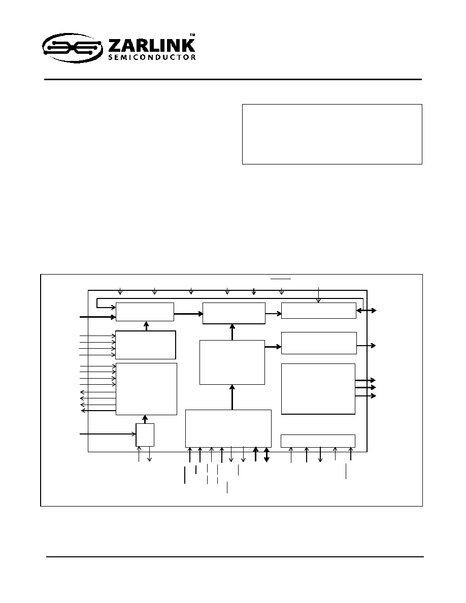
Figure 1 - ZL50015 Functional Block Diagram
Data Memory
Internal Registers &
Microprocessor Interface
Input Timing
Output HiZ
Test Port
Control
OSC
DPLL
S/P Converter
STOHZ[7:0]
FPo[3:0]
CKo[5:0]
STio[15:0]
ODE
RESET
V
SS
V
DD_IO
V
DD_CORE
FPi
CKi
REF0
OSC
i
OSC
o
Connection Memory
MO
T_I
N
TEL
DS
_RD
CS
D[15:
0
]
A[13:0]
TMS
TDi
TDo
TCK
TRST
Output Timing
STi[15:0]
REF1
REF2
REF3
FPo_OFF[2:0]
REF_FAIL0
REF_FAIL1
REF_FAIL2
REF_FAIL3
IR
Q
P/S Converter
DT
A
_RDY
R/W
_WR
OSC_EN
MODE_4M0
MODE_4M1
V
DD_IOA
V
DD_COREA
Zarlink Semiconductor US Patent No. 5,602,884, UK Patent No. 0772912,
France Brevete S.G.D.G. 0772912; Germany DBP No. 69502724.7-08

ZL50015
Data Sheet
2
Zarlink Semiconductor Inc.
∑ Per-stream output bit and fractional bit advancement
∑ Per-channel ITU-T G.711 PCM A-Law/
µ-Law Translation
∑ Four frame pulse and six reference clock outputs
∑ Three programmable delayed frame pulse outputs
∑ Input clock: 4.096 MHz, 8.192 MHz, 16.384 MHz
∑ Input frame pulses: 61 ns, 122 ns, 244 ns
∑ Per-channel constant or variable throughput delay for frame integrity and low latency applications
∑ Per Stream (16) Bit Error Rate Test circuits complying to ITU-O.151
∑ Per-channel high impedance output control
∑ Per-channel message mode
∑ Control interface compatible with Intel and Motorola 16-bit non-multiplexed buses
∑ Connection memory block programming
∑ Supports ST-BUS and GCI-Bus standards for input and output timing
∑ IEEE-1149.1 (JTAG) test port
∑ 3.3 V I/O with 5 V tolerant inputs; 1.8 V core voltage
Applications
∑ PBX and IP-PBX
∑ Small and medium digital switching platforms
∑ Remote access servers and concentrators
∑ Wireless base stations and controllers
∑ Multi service access platforms
∑ Digital Loop Carriers
∑ Computer Telephony Integration

ZL50015
Data Sheet
3
Zarlink Semiconductor Inc.
Description
The ZL50015 is a maximum 1,024 x 1,024 channel non-blocking digital Time Division Multiplex (TDM) switch. It has
sixteen input streams (STi0 - 15) and sixteen output streams (STio0 - 15). The device can switch 64 kbps and
Nx64 kbps TDM channels from any input stream to any output stream. Each of the input and output streams can be
independently programmed to operate at any of the following data rates: 2.048 Mbps, 4.096 Mbps, 8.192 Mbps or
16.384 Mbps. The ZL50015 provides up to eight high impedance control outputs (STOHZ0 - 7) to support the use
of external tristate drivers for the first eight output streams (STio0 - 15). The output streams can be configured to
operate in bi-directional mode, in which case STi0 - 15 will be ignored.
The device contains two types of internal memory - data memory and connection memory. There are four modes of
operation - Connection Mode, Message Mode, BER mode and high impedance mode. In Connection Mode, the
contents of the connection memory define, for each output stream and channel, the source stream and channel
(the actual data to be output is stored in the data memory). In Message Mode, the connection memory is used for
the storage of microprocessor data. Using Zarlink's Message Mode capability, microprocessor data can be
broadcast to the data output streams on a per-channel basis. This feature is useful for transferring control and
status information for external circuits or other TDM devices. In BER mode the output channel data is replaced with
a pseudorandom bit sequence (PRBS) from one of 16 PRBS generators that generates a 2
15
-1 pattern. On the
input side channels can be routed to one of 16 bit error detectors. In high impedance mode the selected output
channel can be put into a high impedance state.
When the device is operating as a timing master, the internal digital PLL is in use. In this mode, an external
20.000 MHz crystal is required for the on-chip crystal oscillator. The DPLL is phase-locked to one of four input
reference signals (which can be 8 kHz, 1.544 MHz, 2.048 MHz, 4.096 MHz, 8.192 MHz, 16.384 MHz or 19.44 MHz
provided on REF0 - 3). The on-chip DPLL operates in normal, holdover or freerun mode and offers jitter
attenuation. The jitter attenuation function exceeds the Stratum 4E specification.
The configurable non-multiplexed microprocessor port allows users to program various device operating modes
and switching configurations. Users can employ the microprocessor port to perform register read/write, connection
memory read/write and data memory read operations. The port is configurable to interface with either Motorola or
Intel-type microprocessors.
The device also supports the mandatory requirements of the IEEE-1149.1 (JTAG) standard via the test port.

ZL50015
Data Sheet
Table of Contents
4
Zarlink Semiconductor Inc.
Features . . . . . . . . . . . . . . . . . . . . . . . . . . . . . . . . . . . . . . . . . . . . . . . . . . . . . . . . . . . . . . . . . . . . . . . . . . . . . . . . . 1
Applications . . . . . . . . . . . . . . . . . . . . . . . . . . . . . . . . . . . . . . . . . . . . . . . . . . . . . . . . . . . . . . . . . . . . . . . . . . . . . 2
Description . . . . . . . . . . . . . . . . . . . . . . . . . . . . . . . . . . . . . . . . . . . . . . . . . . . . . . . . . . . . . . . . . . . . . . . . . . . . . . 3
Changes Summary . . . . . . . . . . . . . . . . . . . . . . . . . . . . . . . . . . . . . . . . . . . . . . . . . . . . . . . . . . . . . . . . . . . . . . . 10
1.0 Pinout Diagrams . . . . . . . . . . . . . . . . . . . . . . . . . . . . . . . . . . . . . . . . . . . . . . . . . . . . . . . . . . . . . . . . . . . . . . 11
1.1 BGA Pinout . . . . . . . . . . . . . . . . . . . . . . . . . . . . . . . . . . . . . . . . . . . . . . . . . . . . . . . . . . . . . . . . . . . . . . . . 11
1.2 QFP Pinout . . . . . . . . . . . . . . . . . . . . . . . . . . . . . . . . . . . . . . . . . . . . . . . . . . . . . . . . . . . . . . . . . . . . . . . . 12
2.0 Pin Description. . . . . . . . . . . . . . . . . . . . . . . . . . . . . . . . . . . . . . . . . . . . . . . . . . . . . . . . . . . . . . . . . . . . . . . . 13
3.0 Device Overview . . . . . . . . . . . . . . . . . . . . . . . . . . . . . . . . . . . . . . . . . . . . . . . . . . . . . . . . . . . . . . . . . . . . . . 20
4.0 Data Rates and Timing . . . . . . . . . . . . . . . . . . . . . . . . . . . . . . . . . . . . . . . . . . . . . . . . . . . . . . . . . . . . . . . . . 21
4.1 External High Impedance Control, STOHZ0 - 7 . . . . . . . . . . . . . . . . . . . . . . . . . . . . . . . . . . . . . . . . . . . . 21
4.2 Input Clock (CKi) and Input Frame Pulse (FPi) Timing . . . . . . . . . . . . . . . . . . . . . . . . . . . . . . . . . . . . . . . 22
5.0 ST-BUS and GCI-Bus Timing . . . . . . . . . . . . . . . . . . . . . . . . . . . . . . . . . . . . . . . . . . . . . . . . . . . . . . . . . . . . 24
6.0 Output Timing Generation . . . . . . . . . . . . . . . . . . . . . . . . . . . . . . . . . . . . . . . . . . . . . . . . . . . . . . . . . . . . . . 24
7.0 Data Input Delay and Data Output Advancement . . . . . . . . . . . . . . . . . . . . . . . . . . . . . . . . . . . . . . . . . . . . 29
7.1 Input Bit Delay Programming. . . . . . . . . . . . . . . . . . . . . . . . . . . . . . . . . . . . . . . . . . . . . . . . . . . . . . . . . . . 29
7.2 Input Bit Sampling Point Programming . . . . . . . . . . . . . . . . . . . . . . . . . . . . . . . . . . . . . . . . . . . . . . . . . . . 30
7.3 Output Advancement Programming . . . . . . . . . . . . . . . . . . . . . . . . . . . . . . . . . . . . . . . . . . . . . . . . . . . . . 31
7.4 Fractional Output Bit Advancement Programming . . . . . . . . . . . . . . . . . . . . . . . . . . . . . . . . . . . . . . . . . . 32
7.5 External High Impedance Control Advancement. . . . . . . . . . . . . . . . . . . . . . . . . . . . . . . . . . . . . . . . . . . . 33
8.0 Data Delay Through the Switching Paths . . . . . . . . . . . . . . . . . . . . . . . . . . . . . . . . . . . . . . . . . . . . . . . . . . 33
8.1 Variable Delay Mode . . . . . . . . . . . . . . . . . . . . . . . . . . . . . . . . . . . . . . . . . . . . . . . . . . . . . . . . . . . . . . . . . 33
8.2 Constant Delay Mode . . . . . . . . . . . . . . . . . . . . . . . . . . . . . . . . . . . . . . . . . . . . . . . . . . . . . . . . . . . . . . . . 34
9.0 Connection Memory Description . . . . . . . . . . . . . . . . . . . . . . . . . . . . . . . . . . . . . . . . . . . . . . . . . . . . . . . . . 35
10.0 Connection Memory Block Programming . . . . . . . . . . . . . . . . . . . . . . . . . . . . . . . . . . . . . . . . . . . . . . . . . 36
10.1 Memory Block Programming Procedure . . . . . . . . . . . . . . . . . . . . . . . . . . . . . . . . . . . . . . . . . . . . . . . . . 36
11.0 Device Operation in Master Mode and Slave Modes . . . . . . . . . . . . . . . . . . . . . . . . . . . . . . . . . . . . . . . . 36
11.1 Master Mode Operation. . . . . . . . . . . . . . . . . . . . . . . . . . . . . . . . . . . . . . . . . . . . . . . . . . . . . . . . . . . . . . 37
11.2 Divided Slave Mode Operation . . . . . . . . . . . . . . . . . . . . . . . . . . . . . . . . . . . . . . . . . . . . . . . . . . . . . . . . 38
11.3 Multiplied Slave Mode Operation. . . . . . . . . . . . . . . . . . . . . . . . . . . . . . . . . . . . . . . . . . . . . . . . . . . . . . . 38
12.0 Overall Operation of the DPLL . . . . . . . . . . . . . . . . . . . . . . . . . . . . . . . . . . . . . . . . . . . . . . . . . . . . . . . . . . 38
12.1 DPLL Timing Modes . . . . . . . . . . . . . . . . . . . . . . . . . . . . . . . . . . . . . . . . . . . . . . . . . . . . . . . . . . . . . . . . 38
12.1.1 Normal Mode . . . . . . . . . . . . . . . . . . . . . . . . . . . . . . . . . . . . . . . . . . . . . . . . . . . . . . . . . . . . . . . . . 38
12.1.2 Holdover Mode. . . . . . . . . . . . . . . . . . . . . . . . . . . . . . . . . . . . . . . . . . . . . . . . . . . . . . . . . . . . . . . . 38
12.1.3 Automatic Mode . . . . . . . . . . . . . . . . . . . . . . . . . . . . . . . . . . . . . . . . . . . . . . . . . . . . . . . . . . . . . . . 38
12.1.3.1 Automatic Reference Switching Without Preferences . . . . . . . . . . . . . . . . . . . . . . . . . . . . . 39
12.1.3.2 Automatic Reference Switching With Preferences . . . . . . . . . . . . . . . . . . . . . . . . . . . . . . . . 40
12.1.4 Freerun Mode. . . . . . . . . . . . . . . . . . . . . . . . . . . . . . . . . . . . . . . . . . . . . . . . . . . . . . . . . . . . . . . . . 42
12.1.5 DPLL Internal Reset Mode. . . . . . . . . . . . . . . . . . . . . . . . . . . . . . . . . . . . . . . . . . . . . . . . . . . . . . . 42
13.0 DPLL Frequency Behaviour . . . . . . . . . . . . . . . . . . . . . . . . . . . . . . . . . . . . . . . . . . . . . . . . . . . . . . . . . . . . 42
13.1 Input Frequencies . . . . . . . . . . . . . . . . . . . . . . . . . . . . . . . . . . . . . . . . . . . . . . . . . . . . . . . . . . . . . . . . . . 42
13.2 Input Frequencies Selection . . . . . . . . . . . . . . . . . . . . . . . . . . . . . . . . . . . . . . . . . . . . . . . . . . . . . . . . . . 42
13.3 Output Frequencies . . . . . . . . . . . . . . . . . . . . . . . . . . . . . . . . . . . . . . . . . . . . . . . . . . . . . . . . . . . . . . . . . 43
13.4 Pull-In/Hold-In Range (also called Locking Range). . . . . . . . . . . . . . . . . . . . . . . . . . . . . . . . . . . . . . . . . 43
14.0 Jitter Performance . . . . . . . . . . . . . . . . . . . . . . . . . . . . . . . . . . . . . . . . . . . . . . . . . . . . . . . . . . . . . . . . . . . . 43
14.1 Input Clock Cycle to Cycle Timing Variation Tolerance. . . . . . . . . . . . . . . . . . . . . . . . . . . . . . . . . . . . . . 43
14.2 Input Jitter Acceptance . . . . . . . . . . . . . . . . . . . . . . . . . . . . . . . . . . . . . . . . . . . . . . . . . . . . . . . . . . . . . . 43
14.3 Jitter Transfer Function . . . . . . . . . . . . . . . . . . . . . . . . . . . . . . . . . . . . . . . . . . . . . . . . . . . . . . . . . . . . . . 43
15.0 DPLL Specific Functions and Requirements . . . . . . . . . . . . . . . . . . . . . . . . . . . . . . . . . . . . . . . . . . . . . . 44
15.1 Lock Detector . . . . . . . . . . . . . . . . . . . . . . . . . . . . . . . . . . . . . . . . . . . . . . . . . . . . . . . . . . . . . . . . . . . . . 44

ZL50015
Data Sheet
Table of Contents
5
Zarlink Semiconductor Inc.
15.2 Maximum Time Interval Error (MTIE) . . . . . . . . . . . . . . . . . . . . . . . . . . . . . . . . . . . . . . . . . . . . . . . . . . . 44
15.3 Phase Alignment Speed (Phase Slope) . . . . . . . . . . . . . . . . . . . . . . . . . . . . . . . . . . . . . . . . . . . . . . . . . 44
15.4 Reference Monitoring . . . . . . . . . . . . . . . . . . . . . . . . . . . . . . . . . . . . . . . . . . . . . . . . . . . . . . . . . . . . . . . 44
15.5 Single Period Reference Monitoring . . . . . . . . . . . . . . . . . . . . . . . . . . . . . . . . . . . . . . . . . . . . . . . . . . . . 45
15.6 Multiple Period Reference Monitoring . . . . . . . . . . . . . . . . . . . . . . . . . . . . . . . . . . . . . . . . . . . . . . . . . . . 45
16.0 Microprocessor Port . . . . . . . . . . . . . . . . . . . . . . . . . . . . . . . . . . . . . . . . . . . . . . . . . . . . . . . . . . . . . . . . . . 46
17.0 Device Reset and Initialization . . . . . . . . . . . . . . . . . . . . . . . . . . . . . . . . . . . . . . . . . . . . . . . . . . . . . . . . . . 46
17.1 Power-up Sequence . . . . . . . . . . . . . . . . . . . . . . . . . . . . . . . . . . . . . . . . . . . . . . . . . . . . . . . . . . . . . . . . 46
17.2 Device Initialization on Reset . . . . . . . . . . . . . . . . . . . . . . . . . . . . . . . . . . . . . . . . . . . . . . . . . . . . . . . . . 46
17.3 Software Reset . . . . . . . . . . . . . . . . . . . . . . . . . . . . . . . . . . . . . . . . . . . . . . . . . . . . . . . . . . . . . . . . . . . . 47
18.0 Pseudo random Bit Generation and Error Detection . . . . . . . . . . . . . . . . . . . . . . . . . . . . . . . . . . . . . . . . 47
19.0 PCM A-law/
µ-law Translation . . . . . . . . . . . . . . . . . . . . . . . . . . . . . . . . . . . . . . . . . . . . . . . . . . . . . . . . . . . 48
20.0 Quadrant Frame Programming. . . . . . . . . . . . . . . . . . . . . . . . . . . . . . . . . . . . . . . . . . . . . . . . . . . . . . . . . . 49
21.0 JTAG Port . . . . . . . . . . . . . . . . . . . . . . . . . . . . . . . . . . . . . . . . . . . . . . . . . . . . . . . . . . . . . . . . . . . . . . . . . . . 49
21.1 Test Access Port (TAP) . . . . . . . . . . . . . . . . . . . . . . . . . . . . . . . . . . . . . . . . . . . . . . . . . . . . . . . . . . . . . . 49
21.2 Instruction Register . . . . . . . . . . . . . . . . . . . . . . . . . . . . . . . . . . . . . . . . . . . . . . . . . . . . . . . . . . . . . . . . . 50
21.3 Test Data Registers. . . . . . . . . . . . . . . . . . . . . . . . . . . . . . . . . . . . . . . . . . . . . . . . . . . . . . . . . . . . . . . . . 50
21.4 BSDL . . . . . . . . . . . . . . . . . . . . . . . . . . . . . . . . . . . . . . . . . . . . . . . . . . . . . . . . . . . . . . . . . . . . . . . . . . . . 50
22.0 Register Address Mapping . . . . . . . . . . . . . . . . . . . . . . . . . . . . . . . . . . . . . . . . . . . . . . . . . . . . . . . . . . . . . 51
23.0 Detailed Register Description . . . . . . . . . . . . . . . . . . . . . . . . . . . . . . . . . . . . . . . . . . . . . . . . . . . . . . . . . . . 53
24.0 Memory . . . . . . . . . . . . . . . . . . . . . . . . . . . . . . . . . . . . . . . . . . . . . . . . . . . . . . . . . . . . . . . . . . . . . . . . . . . . . 86
24.1 Memory Address Mappings. . . . . . . . . . . . . . . . . . . . . . . . . . . . . . . . . . . . . . . . . . . . . . . . . . . . . . . . . . . 86
24.2 Connection Memory Low (CM_L) Bit Assignment. . . . . . . . . . . . . . . . . . . . . . . . . . . . . . . . . . . . . . . . . . 87
24.3 Connection Memory High (CM_H) Bit Assignment . . . . . . . . . . . . . . . . . . . . . . . . . . . . . . . . . . . . . . . . . 88
25.0 Applications . . . . . . . . . . . . . . . . . . . . . . . . . . . . . . . . . . . . . . . . . . . . . . . . . . . . . . . . . . . . . . . . . . . . . . . . . 90
25.1 OSCi Master Clock Requirement . . . . . . . . . . . . . . . . . . . . . . . . . . . . . . . . . . . . . . . . . . . . . . . . . . . . . . 90
25.1.1 External Crystal Oscillator . . . . . . . . . . . . . . . . . . . . . . . . . . . . . . . . . . . . . . . . . . . . . . . . . . . . . . . 90
25.1.2 External Clock Oscillator . . . . . . . . . . . . . . . . . . . . . . . . . . . . . . . . . . . . . . . . . . . . . . . . . . . . . . . . 91
26.0 DC Parameters . . . . . . . . . . . . . . . . . . . . . . . . . . . . . . . . . . . . . . . . . . . . . . . . . . . . . . . . . . . . . . . . . . . . . . . 92
27.0 AC Parameters . . . . . . . . . . . . . . . . . . . . . . . . . . . . . . . . . . . . . . . . . . . . . . . . . . . . . . . . . . . . . . . . . . . . . . . 93

ZL50015
Data Sheet
List of Figures
6
Zarlink Semiconductor Inc.
Figure 1 - ZL50015 Functional Block Diagram . . . . . . . . . . . . . . . . . . . . . . . . . . . . . . . . . . . . . . . . . . . . . . . . . . . . 1
Figure 2 - ZL50015 256-Ball 17 mm x 17 mm PBGA (as viewed through top of package) . . . . . . . . . . . . . . . . . . 11
Figure 3 - ZL50015 256-Lead 28 mm x 28 mm LQFP (top view). . . . . . . . . . . . . . . . . . . . . . . . . . . . . . . . . . . . . . 12
Figure 4 - Input Timing when CKIN1 - 0 bits = "10" in the CR . . . . . . . . . . . . . . . . . . . . . . . . . . . . . . . . . . . . . . . . 23
Figure 5 - Input Timing when CKIN1 - 0 bits = "01" in the CR . . . . . . . . . . . . . . . . . . . . . . . . . . . . . . . . . . . . . . . . 23
Figure 6 - Input Timing when CKIN1 - 0 = "00" in the CR . . . . . . . . . . . . . . . . . . . . . . . . . . . . . . . . . . . . . . . . . . . 24
Figure 7 - Output Timing for CKo0 and FPo0 . . . . . . . . . . . . . . . . . . . . . . . . . . . . . . . . . . . . . . . . . . . . . . . . . . . . 26
Figure 8 - Output Timing for CKo1 and FPo1 . . . . . . . . . . . . . . . . . . . . . . . . . . . . . . . . . . . . . . . . . . . . . . . . . . . . 26
Figure 9 - Output Timing for CKo2 and FPo2 . . . . . . . . . . . . . . . . . . . . . . . . . . . . . . . . . . . . . . . . . . . . . . . . . . . . 27
Figure 10 - Output Timing for CKo3 and FPo3 with CKoFPo3SEL1-0="11" . . . . . . . . . . . . . . . . . . . . . . . . . . . . . 27
Figure 11 - Output Timing for CKo4 . . . . . . . . . . . . . . . . . . . . . . . . . . . . . . . . . . . . . . . . . . . . . . . . . . . . . . . . . . . . 28
Figure 12 - Output Timing for CKo5 and FPo5 (FPo_OFF2) . . . . . . . . . . . . . . . . . . . . . . . . . . . . . . . . . . . . . . . . . 28
Figure 13 - Input Bit Delay Timing Diagram (ST-BUS). . . . . . . . . . . . . . . . . . . . . . . . . . . . . . . . . . . . . . . . . . . . . . 29
Figure 14 - Input Bit Sampling Point Programming . . . . . . . . . . . . . . . . . . . . . . . . . . . . . . . . . . . . . . . . . . . . . . . . 30
Figure 15 - Input Bit Delay and Factional Sampling Point . . . . . . . . . . . . . . . . . . . . . . . . . . . . . . . . . . . . . . . . . . . 31
Figure 16 - Output Bit Advancement Timing Diagram (ST-BUS) . . . . . . . . . . . . . . . . . . . . . . . . . . . . . . . . . . . . . . 32
Figure 17 - Output Fractional Bit Advancement Timing Diagram (ST-BUS) . . . . . . . . . . . . . . . . . . . . . . . . . . . . . 32
Figure 18 - Channel Switching External High Impedance Control Timing . . . . . . . . . . . . . . . . . . . . . . . . . . . . . . . 33
Figure 19 - Data Throughput Delay for Variable Delay . . . . . . . . . . . . . . . . . . . . . . . . . . . . . . . . . . . . . . . . . . . . . 34
Figure 20 - Data Throughput Delay for Constant Delay. . . . . . . . . . . . . . . . . . . . . . . . . . . . . . . . . . . . . . . . . . . . . 35
Figure 21 - No Preferred Reference (Round Robin) with Ref 0-3 available. . . . . . . . . . . . . . . . . . . . . . . . . . . . . . 39
Figure 22 - Automatic Reference Switching State Diagrams with Preferred Reference . . . . . . . . . . . . . . . . . . . . 41
Figure 23 - Crystal Oscillator Circuit . . . . . . . . . . . . . . . . . . . . . . . . . . . . . . . . . . . . . . . . . . . . . . . . . . . . . . . . . . . 90
Figure 24 - Clock Oscillator Circuit. . . . . . . . . . . . . . . . . . . . . . . . . . . . . . . . . . . . . . . . . . . . . . . . . . . . . . . . . . . . . 91
Figure 25 - Timing Parameter Measurement Voltage Levels. . . . . . . . . . . . . . . . . . . . . . . . . . . . . . . . . . . . . . . . . 93
Figure 26 - Motorola Non-Multiplexed Bus Timing - Read Access . . . . . . . . . . . . . . . . . . . . . . . . . . . . . . . . . . . . 94
Figure 27 - Motorola Non-Multiplexed Bus Timing - Write Access. . . . . . . . . . . . . . . . . . . . . . . . . . . . . . . . . . . . . 95
Figure 28 - Intel Non-Multiplexed Bus Timing - Read Access . . . . . . . . . . . . . . . . . . . . . . . . . . . . . . . . . . . . . . . . 96
Figure 29 - Intel Non-Multiplexed Bus Timing - Write Access . . . . . . . . . . . . . . . . . . . . . . . . . . . . . . . . . . . . . . . . 97
Figure 30 - JTAG Test Port Timing Diagram . . . . . . . . . . . . . . . . . . . . . . . . . . . . . . . . . . . . . . . . . . . . . . . . . . . . . 98
Figure 31 - Frame Pulse Input and Clock Input Timing Diagram (ST-BUS). . . . . . . . . . . . . . . . . . . . . . . . . . . . . 100
Figure 32 - Frame Pulse Input and Clock Input Timing Diagram (GCI-Bus) . . . . . . . . . . . . . . . . . . . . . . . . . . . . 100
Figure 33 - ST-BUS Input Timing Diagram when Operated at 2 Mbps, 4 Mbps, 8 Mbps. . . . . . . . . . . . . . . . . . . 101
Figure 34 - ST-BUS Input Timing Diagram when Operated at 16 Mbps . . . . . . . . . . . . . . . . . . . . . . . . . . . . . . . 102
Figure 35 - GCI-Bus Input Timing Diagram when Operated at 2 Mbps, 4 Mbps, 8 Mbps . . . . . . . . . . . . . . . . . . 102
Figure 36 - GCI-Bus Input Timing Diagram when Operated at 16 Mbps . . . . . . . . . . . . . . . . . . . . . . . . . . . . . . . 103
Figure 37 - ST-BUS Output Timing Diagram when Operated at 2, 4, 8 or 16 Mbps . . . . . . . . . . . . . . . . . . . . . . 104
Figure 38 - GCI-Bus Output Timing Diagram when Operated at 2, 4, 8 or 16 Mbps . . . . . . . . . . . . . . . . . . . . . . 105
Figure 39 - Serial Output and External Control . . . . . . . . . . . . . . . . . . . . . . . . . . . . . . . . . . . . . . . . . . . . . . . . . . 106
Figure 40 - Output Drive Enable (ODE) . . . . . . . . . . . . . . . . . . . . . . . . . . . . . . . . . . . . . . . . . . . . . . . . . . . . . . . . 106
Figure 41 - Input and Output Frame Boundary Offset . . . . . . . . . . . . . . . . . . . . . . . . . . . . . . . . . . . . . . . . . . . . . 107
Figure 42 - FPo0 and CKo0 or FPo3 and CKo3 (4.096 MHz) Timing Diagram . . . . . . . . . . . . . . . . . . . . . . . . . . 108
Figure 43 - FPo1 and CKo1 or FPo3 and CKo3 (8.192 MHz) Timing Diagram . . . . . . . . . . . . . . . . . . . . . . . . . . 109
Figure 44 - FPo2 and CKo2 or FPo3 and CKo3 (16.384 MHz) Timing Diagram . . . . . . . . . . . . . . . . . . . . . . . . . 110
Figure 45 - FPo3 and CKo3 (32.768 MHz) Timing Diagram . . . . . . . . . . . . . . . . . . . . . . . . . . . . . . . . . . . . . . . . 111
Figure 46 - FPo4 and CKo4 Timing Diagram (1.544/2.048 MHz) . . . . . . . . . . . . . . . . . . . . . . . . . . . . . . . . . . . . 112
Figure 47 - CKo5 Timing Diagram (19.44 MHz). . . . . . . . . . . . . . . . . . . . . . . . . . . . . . . . . . . . . . . . . . . . . . . . . . 112
Figure 48 - REF0 - 3 Reference Input/Output Timing . . . . . . . . . . . . . . . . . . . . . . . . . . . . . . . . . . . . . . . . . . . . . 114

ZL50015
Data Sheet
List of Figures
7
Zarlink Semiconductor Inc.
Figure 49 - Output Timing (ST-BUS Format) . . . . . . . . . . . . . . . . . . . . . . . . . . . . . . . . . . . . . . . . . . . . . . . . . . . . 116

ZL50015
Data Sheet
List of Tables
8
Zarlink Semiconductor Inc.
Table 1 - CKi and FPi Configurations for Master and Divided Slave Modes . . . . . . . . . . . . . . . . . . . . . . . . . . . . . 22
Table 2 - CKi and FPi Configurations for Multiplied Slave Mode . . . . . . . . . . . . . . . . . . . . . . . . . . . . . . . . . . . . . . 22
Table 3 - Output Timing Generation . . . . . . . . . . . . . . . . . . . . . . . . . . . . . . . . . . . . . . . . . . . . . . . . . . . . . . . . . . . . 25
Table 4 - Delay for Variable Delay Mode . . . . . . . . . . . . . . . . . . . . . . . . . . . . . . . . . . . . . . . . . . . . . . . . . . . . . . . . 34
Table 5 - Connection Memory Low After Block Programming . . . . . . . . . . . . . . . . . . . . . . . . . . . . . . . . . . . . . . . . 36
Table 6 - Connection Memory High After Block Programming. . . . . . . . . . . . . . . . . . . . . . . . . . . . . . . . . . . . . . . . 36
Table 7 - ZL50015 Operating Modes . . . . . . . . . . . . . . . . . . . . . . . . . . . . . . . . . . . . . . . . . . . . . . . . . . . . . . . . . . . 37
Table 8 - Preferred Reference Selection Options . . . . . . . . . . . . . . . . . . . . . . . . . . . . . . . . . . . . . . . . . . . . . . . . . 40
Table 9 - DPLL Input Reference Frequencies . . . . . . . . . . . . . . . . . . . . . . . . . . . . . . . . . . . . . . . . . . . . . . . . . . . . 42
Table 10 - Generated Output Frequencies. . . . . . . . . . . . . . . . . . . . . . . . . . . . . . . . . . . . . . . . . . . . . . . . . . . . . . . 43
Table 11 - Values for Single Period Limits. . . . . . . . . . . . . . . . . . . . . . . . . . . . . . . . . . . . . . . . . . . . . . . . . . . . . . . 45
Table 12 - Multi-Period Hysteresis Limits . . . . . . . . . . . . . . . . . . . . . . . . . . . . . . . . . . . . . . . . . . . . . . . . . . . . . . . . 45
Table 13 - Input and Output Voice and Data Coding . . . . . . . . . . . . . . . . . . . . . . . . . . . . . . . . . . . . . . . . . . . . . . . 48
Table 14 - Definition of the Four Quadrant Frames . . . . . . . . . . . . . . . . . . . . . . . . . . . . . . . . . . . . . . . . . . . . . . . . 49
Table 15 - Quadrant Frame Bit Replacement . . . . . . . . . . . . . . . . . . . . . . . . . . . . . . . . . . . . . . . . . . . . . . . . . . . . 49
Table 16 - Address Map for Registers (A13 = 0) . . . . . . . . . . . . . . . . . . . . . . . . . . . . . . . . . . . . . . . . . . . . . . . . . . 51
Table 17 - Control Register (CR) Bits. . . . . . . . . . . . . . . . . . . . . . . . . . . . . . . . . . . . . . . . . . . . . . . . . . . . . . . . . . . 53
Table 18 - Internal Mode Selection Register (IMS) Bits . . . . . . . . . . . . . . . . . . . . . . . . . . . . . . . . . . . . . . . . . . . . . 56
Table 19 - Software Reset Register (SRR) Bits . . . . . . . . . . . . . . . . . . . . . . . . . . . . . . . . . . . . . . . . . . . . . . . . . . . 57
Table 20 - Output Clock and Frame Pulse Control Register (OCFCR) Bits . . . . . . . . . . . . . . . . . . . . . . . . . . . . . . 58
Table 21 - Output Clock and Frame Pulse Selection Register (OCFSR) Bits . . . . . . . . . . . . . . . . . . . . . . . . . . . . 59
Table 22 - FPo_OFF[n] Register (FPo_OFF[n]) Bits . . . . . . . . . . . . . . . . . . . . . . . . . . . . . . . . . . . . . . . . . . . . . . . 61
Table 23 - Internal Flag Register (IFR) Bits - Read Only . . . . . . . . . . . . . . . . . . . . . . . . . . . . . . . . . . . . . . . . . . . . 62
Table 24 - BER Error Flag Register 0 (BERFR0) Bits - Read Only . . . . . . . . . . . . . . . . . . . . . . . . . . . . . . . . . . . . 62
Table 25 - BER Receiver Lock Register 0 (BERLR0) Bits - Read Only . . . . . . . . . . . . . . . . . . . . . . . . . . . . . . . . . 63
Table 26 - DPLL Control Register (DPLLCR) Bits . . . . . . . . . . . . . . . . . . . . . . . . . . . . . . . . . . . . . . . . . . . . . . . . . 63
Table 27 - Reference Frequency Register (RFR) Bits . . . . . . . . . . . . . . . . . . . . . . . . . . . . . . . . . . . . . . . . . . . . . . 64
Table 28 - Centre Frequency Register - Lower 16 Bits (CFRL) . . . . . . . . . . . . . . . . . . . . . . . . . . . . . . . . . . . . . . . 66
Table 29 - Centre Frequency Register - Upper 10 Bits (CFRU). . . . . . . . . . . . . . . . . . . . . . . . . . . . . . . . . . . . . . . 66
Table 30 - Frequency Offset Register (FOR) Bits - Read Only . . . . . . . . . . . . . . . . . . . . . . . . . . . . . . . . . . . . . . . 67
Table 31 - Lock Detector Threshold Register (LDTR) Bits . . . . . . . . . . . . . . . . . . . . . . . . . . . . . . . . . . . . . . . . . . . 68
Table 32 - Lock Detector Interval Register (LDIR) Bits . . . . . . . . . . . . . . . . . . . . . . . . . . . . . . . . . . . . . . . . . . . . . 68
Table 33 - Slew Rate Limit Register (SRLR) Bits . . . . . . . . . . . . . . . . . . . . . . . . . . . . . . . . . . . . . . . . . . . . . . . . . . 69
Table 34 - Reference Change Control Register (RCCR) Bits . . . . . . . . . . . . . . . . . . . . . . . . . . . . . . . . . . . . . . . . 69
Table 35 - Reference Change Status Register (RCSR) Bits - Read Only . . . . . . . . . . . . . . . . . . . . . . . . . . . . . . . 71
Table 36 - Interrupt Register (IR) Bits - Read Only . . . . . . . . . . . . . . . . . . . . . . . . . . . . . . . . . . . . . . . . . . . . . . . . 72
Table 37 - Interrupt Mask Register (IMR) Bits . . . . . . . . . . . . . . . . . . . . . . . . . . . . . . . . . . . . . . . . . . . . . . . . . . . . 73
Table 38 - Interrupt Clear Register (ICR) Bits . . . . . . . . . . . . . . . . . . . . . . . . . . . . . . . . . . . . . . . . . . . . . . . . . . . . 73
Table 39 - Reference Failure Status Register (RSR) Bits - Read Only . . . . . . . . . . . . . . . . . . . . . . . . . . . . . . . . . 74
Table 40 - Reference Mask Register (RMR) Bits . . . . . . . . . . . . . . . . . . . . . . . . . . . . . . . . . . . . . . . . . . . . . . . . . . 75
Table 41 - Reference Frequency Status Register (RFSR) Bits - Read only. . . . . . . . . . . . . . . . . . . . . . . . . . . . . . 77
Table 42 - Output Jitter Control Register (OJCR) Bits . . . . . . . . . . . . . . . . . . . . . . . . . . . . . . . . . . . . . . . . . . . . . . 79
Table 43 - Stream Input Control Register 0 - 15 (SICR0 - 15) Bits. . . . . . . . . . . . . . . . . . . . . . . . . . . . . . . . . . . . . 79
Table 44 - Stream Input Quadrant Frame Register 0 - 15 (SIQFR0 - 15) Bits . . . . . . . . . . . . . . . . . . . . . . . . . . . . 81
Table 45 - Stream Output Control Register 0 - 15 (SOCR0 - 15) Bits . . . . . . . . . . . . . . . . . . . . . . . . . . . . . . . . . . 83
Table 46 - BER Receiver Start Register [n] (BRSR[n]) Bits . . . . . . . . . . . . . . . . . . . . . . . . . . . . . . . . . . . . . . . . . . 84
Table 47 - BER Receiver Length Register [n] (BRLR[n]) Bits . . . . . . . . . . . . . . . . . . . . . . . . . . . . . . . . . . . . . . . . 84
Table 48 - BER Receiver Control Register [n] (BRCR[n]) Bits . . . . . . . . . . . . . . . . . . . . . . . . . . . . . . . . . . . . . . . . 85

ZL50015
Data Sheet
List of Tables
9
Zarlink Semiconductor Inc.
Table 49 - BER Receiver Error Register [n] (BRER[n]) Bits - Read Only. . . . . . . . . . . . . . . . . . . . . . . . . . . . . . . . 85
Table 50 - Address Map for Memory Locations (A13 = 1) . . . . . . . . . . . . . . . . . . . . . . . . . . . . . . . . . . . . . . . . . . . 86
Table 51 - Connection Memory Low (CM_L) Bit Assignment when CMM = 0 . . . . . . . . . . . . . . . . . . . . . . . . . . . . 87
Table 52 - Connection Memory Low (CM_L) Bit Assignment when CMM = 1 . . . . . . . . . . . . . . . . . . . . . . . . . . . . 88
Table 53 - Connection Memory High (CM_H) Bit Assignment . . . . . . . . . . . . . . . . . . . . . . . . . . . . . . . . . . . . . . . . 89

ZL50015
Data Sheet
10
Zarlink Semiconductor Inc.
Changes Summary
The following table captures the changes from the October 2004 issue.
Page
Item
Change
38, 70, 72 Section 12.1, "DPLL Timing Modes" on
page 38
RCCR Register bits "FDM1 - 0" on page 70
RCCR Register bits "DPM1 - 0" on page 72
∑ The on-chip DPLL's normal, holdover, automatic,
and freerun modes are now collectively referred
to as DPLL timing modes instead of operation
modes. This change is to avoid confusion with
the two main device operating modes; the
master and slave modes.
39
12.1.3.1, "Automatic Reference Switching
Without Preferences" and 12.1.3.2,
"Automatic Reference Switching With
Preferences"
∑ Added two new sections, Section 12.1.3.1 and
Section 12.1.3.2 to clarify the DPLL's automatic
reference switching with and without preference
operations in Automatic Timing Mode.
68
Table 31, Lock Detector Threshold
Register (LDTR) Bits
∑ Clarified threshold calculations.
70
Table 34, Reference Change Control
Register (RCCR) Bits
∑ Added description to clarify that only two
consecutive references can be used in
automatic timing mode with a preferred
reference.
ZL50015
Data Sheet
11
Zarlink Semiconductor Inc.
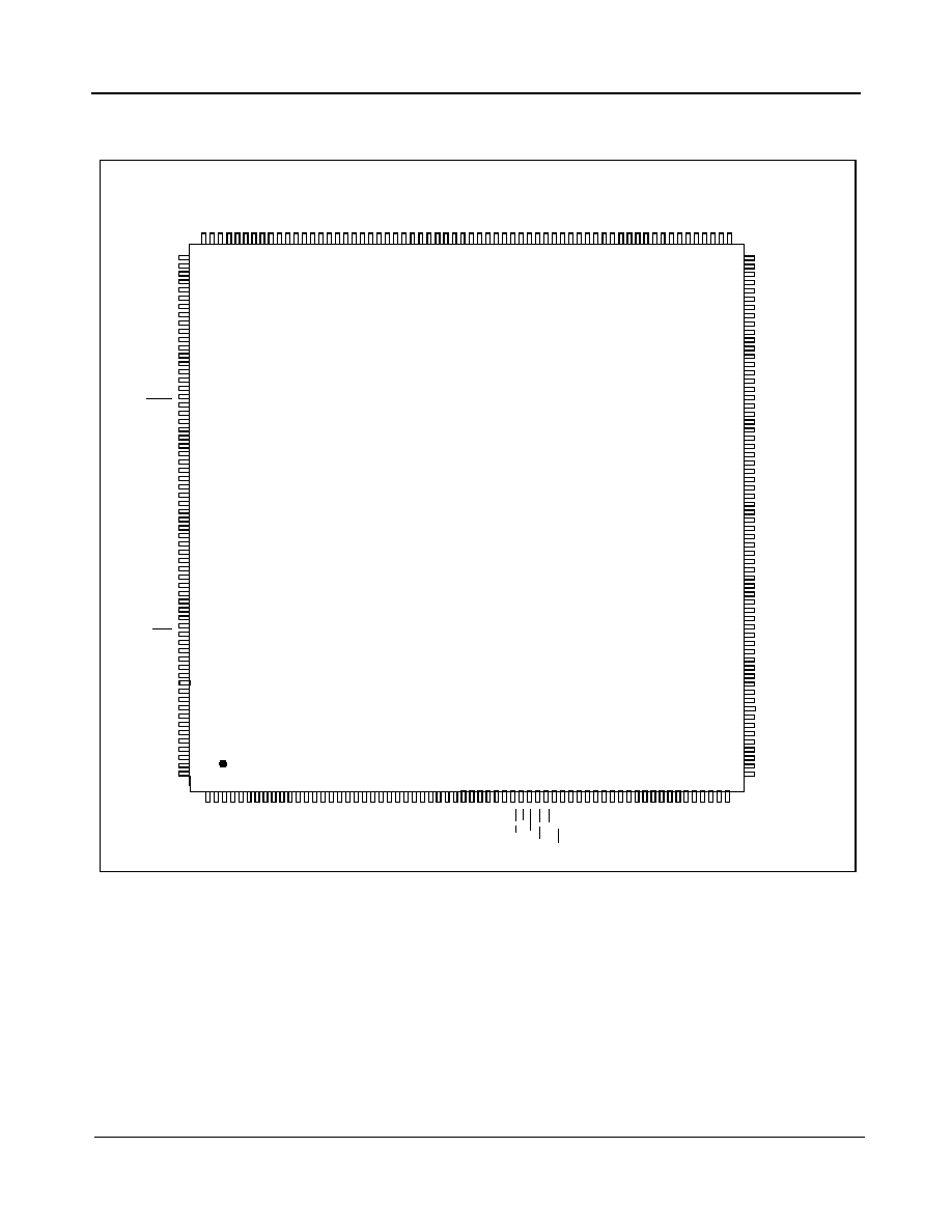
1.0 Pinout Diagrams
1.1 BGA Pinout
Figure 2 - ZL50015 256-Ball 17 mm x 17 mm PBGA (as viewed through top of package)
1
2
3
4
5
6
7
8
9
10
11
12
13
14
15
16
A
V
SS
NC
NC
NC
NC
NC
NC
NC
NC
NC
NC
NC
NC
NC
NC
V
SS
A
B
NC
STi10
STi5
STi4
CKo2
STi0
CKo0
REF2
V
DD_
COREA
FPi
CKi
IC_Open IC_Open
OSCi
ODE
NC
B
C
NC
STi9
V
SS
STi7
STi6
STi1
CKo1
REF_
FAIL2
V
SS
IC_Open IC_Open
OSCo
IC_GND
V
SS
STio15
NC
C
D
NC
STi11
V
DD_IO
STi3
STi2
CKo4
REF3
REF1
REF_
FAIL0
V
SS
FPo_
OFF1
OSC_
EN
STio13
V
DD_IO
STio14
NC
D
E
NC
STi14
STi8
V
DD_IO
V
SS
V
DD_
CORE
REF_
FAIL3
REF_
FAIL1
REF0
NC
V
DD_
CORE
V
SS
V
DD_IO
STio12
FPo2
NC
E
F
NC
STi15
STi12
STi13
V
DD_IO
V
DD_
CORE
V
DD_
CORE
V
SS
V
SS
V
DD_
CORE
V
DD_
CORE
V
DD_IO
IC_Open
FPo3
FPo_
OFF2
NC
F
G
NC
RESET
IC_GND IC_Open
TDo
V
DD_IO
V
SS
V
SS
V
SS
V
SS
V
DD_IO
A12
A13
FPo1
FPo0
NC
G
H
NC
V
SS
V
SS
V
DD_
COREA
CKo5
V
SS
V
SS
V
SS
V
SS
V
SS
A7
A9
A10
FPo_
OFF0
A11
NC
H
J
NC
V
DD_IOA
V
DD_IOA
V
SS
V
SS
CKo3
V
SS
V
SS
V
SS
V
SS
A3
A4
A5
A8
A6
NC
J
K
NC
V
SS
TMS
V
SS
V
DD_
COREA
V
DD_IO
V
SS
V
SS
V
SS
V
SS
V
DD_IO
IC_Open
A0
A2
A1
NC
K
L
NC
V
DD_
COREA
TRST
TCK
V
DD_IO
V
DD_
CORE
V
DD_
CORE
V
SS
V
SS
V
DD_
CORE
V
DD_
CORE
V
DD_IO
STio10
STio11
STio9
NC
L
M
NC
NC
TDi
D0
V
SS
V
DD_
CORE
V
DD_
CORE
D6
D10
V
DD_
CORE
V
DD_
CORE
V
SS
MOT
_INTEL
MODE_
4M0
STio8
NC
M
N
NC
NC
V
DD_IO
STio0
STOHZ3
D1
D5
D7
D11
D13
R/W
_WR
DTA_
RDY
STio4
V
DD_IO
STOHZ5
NC
N
P
NC
NC
V
SS
STio1
STio3
STOHZ1
D3
D8
D14
IRQ
STio5
STOHZ4 STOHZ6
V
SS
STOHZ7
NC
P
R
NC
NC
STOHZ0
STio2
STOHZ2
D2
D4
D9
D12
D15
CS
DS_RD
MODE_
4M1
STio6
STio7
NC
R
T
V
SS
NC
NC
NC
NC
NC
NC
NC
NC
NC
NC
NC
NC
NC
NC
V
SS
T
1
2
3
4
5
6
7
8
9
10
11
12
13
14
15
16
Note: A1 corner identified by metallized marking.
Note: Pinout is shown as viewed through top of package.
ZL50015
Data Sheet
12
Zarlink Semiconductor Inc.
1.2 QFP Pinout
Figure 3 - ZL50015 256-Lead 28 mm x 28 mm LQFP (top view)
152
154
156
158
160
162
164
166
168
170
172
174
176
178
180
22 24 26 28 30
20
18
16
14
12
10
8
6
4
2
120
102
104
106
108
110
114
116
118
112
52 54 56
58 60
50
48
46
44
42
40
38
36
34
32
100
82
84
86
88
90
94
96
98
92
80
66
68
70
74
76
78
72
132
134
136
138
140
142
144
146
148
150
CK
i
FP
i
IC_
O
p
e
n
IC_
O
p
e
n
IC_
O
p
e
n
IC_
O
p
e
n
OS
C
o
OS
C
i
V
DD_
IO
VS
S
IC_
G
ND
OD
E
V
DD_
IO
NC NC NC NC
62 64
122
124
126
128
182
184
186
188
190
NC NC
VS
S
VD
D
_
I
O
ST
i_7
ST
i_6
ST
i_
3
ST
i_
2
ST
i_
1
ST
i_
0
CK
o
4
VS
S
RE
F_
FA
I
L
2
RE
F2
RE
F_
FA
I
L
1
RE
F
1
RE
F_
FA
I
L
0
RE
F0
VS
S
NC
NC
ST
i_
5
ST
i_
4
VD
D
_
I
O
CK
o
2
CK
o
1
VS
S
V
D
D
_
CO
RE
CK
o
0
VSS
V
DD_
IO
RE
F_
FA
I
L
3
RE
F
3
VS
S
V
DD_
CO
RE
A
NC
VDD_IO
NC
NC
NC
NC
NC
NC
VDD_IO
TRST
TCK
TMS
VSS
VDD_CORE
VSS
VDD_COREA
VSS
VSS
CKo3
VDD_IOAAA
VDD_COREA
VSS
VSS
CKo5
VDD_IOA
VSS
VDD_COREA
VSS
VSS
VDD_CORE
TDo
RESET
IC_Open
IC_GND
VSS
VDD_IO
STi_15
STi_14
STi_11
STi_10
STi_9
STi_8
NC
NC
NC
VSS
TDi
NC
VDD_IO
NC
202
220
218
216
214
212
208
206
204
210
222
240
238
236
234
232
228
226
224
230
242
256
254
252
248
246
244
250
200
198
196
194
VSS
STi_13
STi_12
NC NC
NC NC
VDD_I
O
VSS
S
T
i
o_0
S
T
i
o_1
S
T
i
o_2
S
T
i
o_3
STOH
Z
_
0
S
T
OHZ_1
STOH
Z
_
2
STOH
Z
_
3
VDD_I
O
VS
S
D0
V
D
D
_
CO
RE
VS
S
D1
D2
D3
D4 D5
D7 D8 D9
D6
VDD_I
O
VSS
D1
0
V
D
D
_
CO
RE
VS
S
D1
1
D1
2
D1
3
D1
4
D1
5
R/
W
_W
R
CS
M
O
T_I
N
TE
L
DS
_R
D
IR
Q
DT
A
_RDY
MO
DE
_
4
M0
V
D
D
_
CO
RE
VS
S
M
O
D
E
_4M
1
VDD_I
O
VSS
S
T
i
o_4
S
T
i
o_5
S
T
i
o_6
S
T
i
o_7
STOH
Z
_
4
ST
OH
Z
_
5
STOH
Z
_
6
ST
OH
Z_7
VDD_IO
VS
S
NC
NC
NC
NC
NC
VDD_IO
VSS
STio_8
STio_9
STio_10
STio_11
NC
NC
NC
NC
VDD_IO
IC_Open
VSS
VDD_CORE
VSS
A0
A1
A2
A3
A4
A7
A6
A5
A11
A10
A9
A8
VDD_CORE
VSS
A13
A12
IC_Open
VDD_IO
VSS
FPo_OFF0
FPo0
FPo_OFF1
FPo1
FPo2
FPo_OFF2
FPo3
VDD_CORE
VSS
OSC_EN
VDD_IO
VSS
STio_12
STio_13
STio_14
STio_15
NC
NC
NC
NC
VDD_IO
VSS
NC
NC
NC
NC
NC
NC
NC
NC
NC
NC
NC
VS
S
V
DD_
CO
RE
VS
S
VS
S
V
DD_
IO
NC
NC
NC
NC
VSS
NC
NC
NC
192
130
NC
NC
NC
NC NC
NC

ZL50015
Data Sheet
13
Zarlink Semiconductor Inc.
2.0 Pin Description
PBGA Pin
Number
LQFP Pin
Number
Pin Name
Description
E6, E11, F6,
F7, F10,
F11, L6, L7,
L10, L11,
M6, M7,
M10, M11
19, 33,
45, 83,
95, 109,
146, 173,
213, 233
V
DD_CORE
Power Supply for the core logic: +1.8 V
H4, K5, B9,
L2
217, 231,
157, 224
V
DD_COREA
Power Supply for analog circuitry: +1.8 V
D3, D14, E4,
E13, F5,
F12, G6,
G11, K6,
K11, L5,
L12, N3,
N14
5, 15, 29,
49, 57,
69, 79,
101, 113,
121, 133,
143, 160,
169, 177,
186, 195,
207, 241,
249
V
DD_IO
Power Supply for I/O: +3.3 V
J2, J3
220, 226
V
DD_IOA
Power Supply for the CKo5 and CKo3 outputs: +3.3 V
A1, A16, C3,
C9, C14,
D10, E5,
E12, F8, F9,
G7, G8, G9,
G10, H2,
H3, H6, H7,
H8, H9,
H10, J4, J5,
J7, J8, J9,
J10, K2, K4,
K7, K8, K9,
K10, L8, L9,
M5, M12,
P3, P14, T1,
T16
8, 17, 21,
31, 35,
47, 50,
60, 71,
81, 85,
97, 103,
111, 114,
123, 142,
145, 147,
156, 158,
162, 171,
175, 178,
188, 199,
209, 214,
216, 218,
222, 223,
228, 230,
232, 235,
242, 251
V
SS
Ground

ZL50015
Data Sheet
14
Zarlink Semiconductor Inc.
K3
234
TMS
Test Mode Select (5 V-Tolerant Input with Internal Pull-up)
JTAG signal that controls the state transitions of the TAP controller.
This pin is pulled high by an internal pull-up resistor when it is not
driven.
L4
238
TCK
Test Clock (5 V-Tolerant Schmitt-Triggered Input with Internal
Pull-up)
Provides the clock to the JTAG test logic.
L3
239
TRST
Test Reset (5 V-Tolerant Input with Internal Pull-up)
Asynchronously initializes the JTAG TAP controller by putting it in
the Test-Logic-Reset state. This pin should be pulsed low during
power-up to ensure that the device is in the normal functional
mode. When JTAG is not being used, this pin should be pulled low
during normal operation.
M3
240
TDi
Test Serial Data In (5 V-Tolerant Input with Internal Pull-up)
JTAG serial test instructions and data are shifted in on this pin.
This pin is pulled high by an internal pull-up resistor when it is not
driven.
G5
212
TDo
Test Serial Data Out (5 V-Tolerant Three-state Output)
JTAG serial data is output on this pin on the falling edge of TCK.
This pin is held in high impedance state when JTAG is not
enabled.
B12, B13,
C10, C11,
F13, G4,
K12
80, 105,
150, 151,
152, 153,
210
IC_Open
Internal Test Mode (5 V-Tolerant Input with Internal Pull-down)
These pins may be left unconnected.
C13, G3
144, 208
IC_GND
Internal Test Mode Enable (5 V-Tolerant Input)
These pins MUST be low.
PBGA Pin
Number
LQFP Pin
Number
Pin Name
Description

ZL50015
Data Sheet
15
Zarlink Semiconductor Inc.
A8, A9, A14,
A15, E10,
M2, N2, P2,
P16, R2,
R16, T6, T7,
T8, T9, T10,
T11, T12,
T13, T14,
T15, D16,
E16, C16,
B16, A13,
A12, A10,
A11, N1,
M1, P1, R1,
T2, T3, T5,
T4, N16,
M16, L16,
K16, H16,
J16, G16,
F16, E1, D1,
G1, F1, J1,
H1, K1, L1,
A7, A5, A6,
A4, A3, A2,
C1, B1
61, 62,
63, 64,
65, 66,
67, 68,
134, 135,
136, 137,
138, 139,
140, 215,
219, 225,
229, 236,
237, 125,
126, 127,
128, 129,
130, 131,
132, 253,
254, 255,
256, 1, 2,
3, 4, 75,
76, 77,
78, 119,
120, 122,
124, 243,
244, 245,
246, 247,
248, 250,
252, 189,
190, 191,
192, 193,
194, 196,
197
NC
No Connect
These pins MUST be left unconnected.
M14, R13
46, 48
MODE_4M0,
MODE_4M1
4 M Input Clock Mode 0 to 1 (5 V-Tolerant Input with internal
pull-down) These two pins should be tied together and are
typically used to select CKi = 4.096 MHz operation. See Table 7,
"ZL50015 Operating Modes" on page 37 for a detailed explanation.
See Table 17, "Control Register (CR) Bits" on page 53 for CKi and
FPi selection using the CKIN1 - 0 bits.
D12
107
OSC_EN
Oscillator Enable (5 V-Tolerant Input with Internal Pull-down) If
tied high, this pin indicates that there is a 20 MHz external
oscillator interfacing with the device. If tied low, there is no
oscillator and CKi will be used for master clock generation.
If the device is in master mode, an external oscillator is required
and this pin MUST be tied high.
PBGA Pin
Number
LQFP Pin
Number
Pin Name
Description

ZL50015
Data Sheet
16
Zarlink Semiconductor Inc.
C12
149
OSCo
Oscillator Clock Output (3.3 V Output)
If OSC_EN = `1', this pin should be connected to a 20 MHz crystal
(see Figure 23 on page 90) or left unconnected if a clock oscillator
is connected to OSCi pin under normal operation (see Figure 24
on page 91). If OSC_EN = 0, this pin MUST be left unconnected.
B14
148
OSCi
Oscillator Clock Input (3.3 V Input)
If OSC_EN = `1', this pin should be connected to a 20 MHz crystal
(see Figure 23 on page 90) or to a clock oscillator under normal
operation (see Figure 24 on page 91). If OSC_EN = 0, this pin
MUST be driven high or low by connecting either to V
DD_IO
or to
ground.
E9, D8, B8,
D7
161, 164,
166, 168
REF0 - 3
DPLL Reference Inputs 0 to 3 (5 V-Tolerant Schmitt-Triggered
Inputs)
If the device is in Master mode, these input pins accept 8 kHz,
1.544 MHz, 2.048 MHz, 4.096 MHz, 8.192 MHz, 16.384 MHz or
19.44 MHz timing references independently. One of these inputs is
defined as the preferred or forced input reference for the DPLL.
The Reference Change Control Register (RCCR) selects the
control of the preferred reference.These pins are ignored if the
device is in slave mode unless SLV_DPLLEN (bit 13) in the
Control Register (CR) is set. When these input pins are not in use,
they MUST be driven high or low by connecting either to V
DD_IO
or
to ground.
D9, E8, C8,
E7
159, 163,
165, 167
REF_FAIL0 - 3
Failure Indication for DPLL References 0 to 3 (5 V-Tolerant
Three-state Outputs)
These output pins are used to indicate input reference failure when
the device is in master mode.
If REF0 fails, REF_FAIL0 will be driven high.
If REF1 fails, REF_FAIL1 will be driven high.
If REF2 fails, REF_FAIL2 will be driven high.
If REF3 fails, REF_FAIL3 will be driven high.
If the device is in slave mode, these pins are driven low, unless
SLV_DPLLEN (bit 13) in the Control Register (CR) is set.
G15, G14,
E15, F14
102, 106,
110, 112
FPo0 - 3
ST-BUS/GCI-Bus Frame Pulse Outputs 0 to 3 (5 V-Tolerant
Three-state Outputs)
FPo0: 8 kHz frame pulse corresponding to the 4.096 MHz output
clock of CKo0.
FPo1: 8 kHz frame pulse corresponding to the 8.192 MHz output
clock of CKo1.
FPo2: 8 kHz frame pulse corresponding to 16.384 MHz output
clock of CKo2.
FPo3: Programmable 8 kHz frame pulse corresponding to
4.096 MHz, 8.192 MHz, 16.384 MHz, or 32.768 MHz output clock
of CKo3.
In Divided Slave modes, the frame pulse width of FPo0 - 3 cannot
be narrower than the input frame pulse (FPi) width.
PBGA Pin
Number
LQFP Pin
Number
Pin Name
Description

ZL50015
Data Sheet
17
Zarlink Semiconductor Inc.
H14, D11
100, 104
FPo_OFF0 - 1
Generated Offset Frame Pulse Outputs 0 to 1 (5 V-Tolerant
Three-state Outputs)
Individually programmable 8 kHz frame pulses, offset from the
output frame boundary by a programmable number of channels.
F15
108
FPo_OFF2
or
FPo5
Generated Offset Frame Pulse Output 2 or 19.44 MHz Frame
Pulse Output (5 V-Tolerant Three-state Output)
As FPo_OFF2, this is an individually programmable 8 kHz frame
pulse, offset from the output frame boundary by a programmable
number of channels.
By programming the FP19EN (bit 10) of FPOFF2 register to high,
this signal becomes FPo5, a non-offset frame pulse corresponding
to the 19.44 MHz clock presented on CKo5. FPo5 is only available
in Master mode or when the SLV_DPLLEN bit in the Control
Register is set high while the device is in one of the slave modes.
B7, C7, B5,
J6, D6, H5
170, 172,
174, 227,
176, 221
CKo0 - 5
ST-BUS/GCI-Bus Clock Outputs 0 to 5 (5 V-Tolerant
Three-state Outputs)
CKo0: 4.096 MHz output clock.
CKo1: 8.192 MHz output clock.
CKo2: 16.384 MHz output clock.
CKo3: 4.096 MHz, 8.192 MHz, 16.384 MHz or 32.768 MHz
programmable output clock.
CKo4: 1.544 MHz or 2.048 MHz programmable output clock.
CKo5: 19.44 MHz output clock.
See Section 6.0 on page 24 for details. In Divided Slave mode, the
frequency of CKo0 - 3 cannot be higher than input clock (CKi).
CKo4 and CKo5 are only available in Master mode or when the
SLV_DPLLEN bit in the Control Register is set high while the
device is in one of the slave modes.
B10
155
FPi
ST-BUS/GCI-Bus Frame Pulse Input (5 V-Tolerant
Schmitt-Triggered Input)
This pin accepts the frame pulse which stays active for 61 ns,
122 ns or 244 ns at the frame boundary. The frame pulse
frequency is 8 kHz. The frame pulse associated with the highest
input or output data rate must be applied to this pin when the
device is operating in Divided Slave mode or Master mode. The
exception is if the device is operating in Master mode with
loopback (i.e., CKi_LP is set in the Control Register). In that case,
this input must be tied high or low externally. When the device is
operating in Multiplied Slave mode, the frame pulse associated
with the highest input data rate must be applied to this pin. For all
modes (except Master mode with loopback), if the data rate is
16.384 Mbps, a 61 ns wide frame pulse must be used. By default,
the device accepts a negative frame pulse in ST-BUS format, but it
can accept a positive frame pulse instead if the FPINP bit is set
high in the Control Register (CR). It can accept a GCI-formatted
frame pulse by programming the FPINPOS bit in the Control
Register (CR) to high.
PBGA Pin
Number
LQFP Pin
Number
Pin Name
Description

ZL50015
Data Sheet
18
Zarlink Semiconductor Inc.
B11
154
CKi
ST-BUS/GCI-Bus Clock Input (5 V-Tolerant Schmitt Triggered
Input)
This pin accepts a 4.096 MHz, 8.192 MHz or 16.384 MHz clock.
The clock frequency associated with twice the highest input or
output data rate must be applied to this pin when the device is
operating in either Divided Slave mode or Master mode. The
exception is if the device is operating in Master mode with
loopback (i.e., CKi_LP is set in the Control Register). In that case,
this input must be tied high or low externally. The clock frequency
associated with twice the highest input data rate must be applied
to this pin when the device is operating in Multiplied Slave mode.
In all modes of operation (except Master mode with loopback),
when data is running at 16.384 Mbps, a 16.384 MHz clock must be
used. By default, the clock falling edge defines the input frame
boundary, but the device allows the clock rising edge to define the
frame boundary by programming the CKINP bit in the Control
Register (CR).
B6, C6, D5,
D4, B4, B3,
C5, C4, E3,
C2, B2, D2,
F3, F4, E2,
F2
179, 180,
181, 182,
183, 184,
185, 187,
198, 200,
201, 202,
203, 204,
205, 206
STi0 - 15
Serial Input Streams 0 to 15 (5 V-Tolerant Inputs with Enabled
Internal Pull-downs)
The data rate of each input stream can be selected independently
using the Stream Input Control Registers (SICR[n]). In the
2.048 Mbps mode, these pins accept serial TDM data streams at
2.048 Mbps with 32 channels per frame. In the 4.096 Mbps mode,
these pins accept serial TDM data streams at 4.096 Mbps with 64
channels per frame. In the 8.192 Mbps mode, these pins accept
serial TDM data streams at 8.192 Mbps with 128 channels per
frame. In the 16.384 Mbps mode, these pins accept TDM data
streams at 16.384 Mbps with 256 channels per frame.
N4, P4, R4,
P5, N13,
P11, R14,
R15, M15,
L15, L13,
L14, E14,
D13, D15,
C15
6, 7, 9,
10, 51,
52, 53,
54, 70,
72, 73,
74, 115,
116, 117,
118
STio 0 - 15
Serial Output Streams 0 to 15 (5 V-Tolerant Slew-Rate-Limited
Three-state I/Os with Enabled Internal Pull-downs)
The data rate of each output stream can be selected
independently using the Stream Output Control Registers
(SOCR[n]). In the 2.048 Mbps mode, these pins output serial TDM
data streams at 2.048 Mbps with 32 channels per frame. In the
4.096 Mbps mode, these pins output serial TDM data streams at
4.096 Mbps with 64 channels per frame. In the 8.192 Mbps mode,
these pins output serial TDM data streams at 8.192 Mbps with 128
channels per frame. In the 16.384 Mbps mode, these pins output
serial TDM data streams at 16.384 Mbps with 256 channels per
frame.These output streams can be used as bi-directionals by
programming BDL (bit 6) of Internal Mode Selection (IMS) register.
PBGA Pin
Number
LQFP Pin
Number
Pin Name
Description

ZL50015
Data Sheet
19
Zarlink Semiconductor Inc.
R3, P6, R5,
N5, P12,
N15, P13,
P15
11, 12,
13, 14,
55, 56,
58, 59
STOHZ 0 - 7
Serial Output Streams High Impedance Control 0 to 7
(5 V-Tolerant Slew-Rate-Limited Three-state Outputs)
These pins are used to enable (or disable) external three-state
buffers. When an output channel is in the high impedance state,
the STOHZ drives high for the duration of the corresponding output
channel. When the STio channel is active, the STOHZ drives low
for the duration of the corresponding output channel. STOHZ
outputs are available for STio0 - only.
B15
141
ODE
Output Drive Enable (5 V-Tolerant Input with Internal Pull-up)
This is the output enable control for STio0 - 15 and the
output-driven-high control for STOHZ0 - 7. When it is high, STio0 -
15 and STOHZ0 - 7 are enabled. When it is low, STio0 - 15 are
tristated and STOHZ0 - 7 are driven high.
M4, N6, R6,
P7, R7, N7,
M8, N8, P8,
R8, M9, N9,
R9, N10, P9,
R10
16, 18,
20, 22,
23, 24,
25, 26,
27, 28,
30, 32,
34, 36,
37, 38
D0 - 15
Data Bus 0 to 15 (5 V-Tolerant Slew-Rate-Limited Three-state
I/Os)
These pins form the 16-bit data bus of the microprocessor port.
N12
44
DTA_RDY
Data Transfer Acknowledgment_Ready (5 V-Tolerant
Three-state Output)
This active low output indicates that a data bus transfer is
complete for the Motorola interface. For the Intel interface, it
indicates a transfer is completed when this pin goes from low to
high. An external pull-up resistor MUST hold this pin at HIGH level
for the Motorola mode. An external pull-down resistor MUST hold
this pin at LOW level for the Intel mode.
R11
40
CS
Chip Select (5 V-Tolerant Input)
Active low input used by the Motorola or Intel microprocessor to
enable the microprocessor port access.
N11
39
R/W_WR
Read/Write_Write (5 V-Tolerant Input)
This input controls the direction of the data bus lines (D0 - 15)
during a microprocessor access. For the Motorola interface, this
pin is set high and low for the read and write access respectively.
For the Intel interface, a write access is indicated when this pin
goes low.
R12
42
DS_RD
Data Strobe_Read (5 V-Tolerant Input)
This active low input works in conjunction with CS to enable the
microprocessor port read and write operations for the Motorola
interface. A read access is indicated when it goes low for the Intel
interface.
PBGA Pin
Number
LQFP Pin
Number
Pin Name
Description

ZL50015
Data Sheet
20
Zarlink Semiconductor Inc.
3.0 Device Overview
The device has sixteen ST-BUS/GCI-Bus inputs (STi0 - 15) and sixteen ST-BUS/GCI-Bus outputs (STio0 - 15).
STio0 - 15 can also be configured as bi-directional pins, in which case STi0 - 15 will be ignored. It is a non-blocking
digital switch with 1024 64 kbps channels and is capable of performing rate conversion between ST-BUS/GCI-Bus
inputs and ST-BUS/GCI-Bus outputs. The ST-BUS/GCI-Bus inputs accept serial input data streams with data rates
of 2.048 Mbps, 4.096 Mbps, 8.192 Mbps and 16.384 Mbps on a per-stream basis. The ST-BUS/GCI-Bus outputs
deliver serial data streams with data rates of 2.048 Mbps, 4.096 Mbps and, 8.192 Mbps and 16.384 Mbps on a
per-stream basis. The device also provides eight high impedance control outputs (STOHZ0 - 7) to support the use
of external ST-BUS/GCI-Bus tristate drivers for the first eight ST-BUS/GCI-Bus outputs (STio0 -7).
By using Zarlink's message mode capability, microprocessor data stored in the connection memory can be
broadcast to the output streams on a per-channel basis. This feature is useful for transferring control and status
information for external circuits or other ST-BUS/GCI-Bus devices.
The device uses the ST-BUS/GCI-Bus input frame pulse (FPi) and the ST-BUS/GCI-Bus input clock (CKi) to define
the input frame boundary and timing for sampling the ST-BUS/GCI-Bus input streams with various data rates. The
output data streams will be driven by and have their timing defined by FPi and CKi in Divided Slave mode. In
Multiplied Slave mode, the output data streams will be driven by an internally generated clock, which is multiplied
K13, K15,
K14, J11,
J12, J13,
J15, H11,
J14, H12,
H13, H15,
G12, G13
82, 84,
86, 87,
88, 89,
90, 91,
92, 93,
94, 96,
98, 99
A0 - 13
Address 0 to 13 (5 V-Tolerant Inputs)
These pins form the 14-bit address bus to the internal memories
and registers.
M13
41
MOT_INTEL
Motorola_Intel (5 V-Tolerant Input with Enabled Internal
Pull-up)
This pin selects the Motorola or Intel microprocessor interface to
be connected to the device. When this pin is unconnected or
connected to high, Motorola interface is assumed. When this pin is
connected to ground, Intel interface should be used.
P10
43
IRQ
Interrupt (5 V-Tolerant Three-state Output)
This programmable active low output indicates that the internal
operating status of the DPLL has changed. An external pull-up
resistor MUST hold this pin at HIGH level.
G2
211
RESET
Device Reset (5 V-Tolerant Input with Internal Pull-up)
This input (active LOW) puts the device in its reset state that
disables the STio0 - 15 drivers and drives the STOHZ0 - 7 outputs
to high. It also preloads registers with default values and clears all
internal counters. To ensure proper reset action, the reset pin must
be low for longer than 1
µs. Upon releasing the reset signal to the
device, the first microprocessor access cannot take place for at
least 600
µs due to the time required to stabilize the device and
the crystal oscillator from the power-down state. Refer to Section
Section 17.2 on page 46 for details.
PBGA Pin
Number
LQFP Pin
Number
Pin Name
Description

ZL50015
Data Sheet
21
Zarlink Semiconductor Inc.
from CKi internally. In Master mode, the on-chip DPLL will drive the output data streams and provide output clocks
and frame pulses. Refer to Application Note ZLAN-120 for further explanation of the different modes of operation.
When the device is in Master mode, the DPLL is phase-locked to one of four DPLL reference signals, REF0 - 3,
which are sourced by an external 8 kHz, 1.544 MHz, 2.048 MHz, 4.096 MHz, 8.192 MHz, 16.384 MHz or
19.44 MHz reference signal. The on-chip DPLL also offers jitter attenuation, reference switching, reference
monitoring, freerun and holdover functions. The jitter performance exceeds the Stratum 4E specification. The
intrinsic jitter of all output clocks is less than 1 ns (except for the 1.544 MHz output).
There are two slave modes for this device:
The first is the Divided Slave mode. In this mode, output streams are clocked by input CKi. Therefore the output
streams have exactly the same jitter as the input streams. The output data rate can be the same as or lower than
the input data rate, but the output data rate cannot be higher than what CKi can drive. For example, if CKi is
4.096 MHz, the output data rate cannot be higher than 2.048 Mbps. The second slave mode is called Multiplied
Slave mode. In this mode, CKi is used to generate a 16.384 MHz clock internally, and output streams are driven by
this 16.384 MHz clock. In Multiplied Slave mode, the data rate of output streams can be any rate, but output jitter
may not be exactly the same as input jitter.
A Motorola or Intel compatible non-multiplexed microprocessor port allows users to program the device to operate
in various modes under different switching configurations. Users can use the microprocessor port to perform
internal register and memory read and write operations. The microprocessor port has a 16-bit data bus, a 14-bit
address bus and six control signals (MOT_INTEL, CS, DS_RD, R/W_WR, IRQ and DTA_RDY).
The device supports the mandatory requirements of the IEEE-1149.1 (JTAG) standard via the test port.
4.0 Data Rates and Timing
The ZL50015 has 16 serial data inputs and 16 serial data outputs. Each stream can be individually programmed to
operate at 2.048 Mbps, 4.096 Mbps, 8.192 Mbps or 16.384 Mbps. Depending on the data rate there will be 32
channels, 64 channels, 128 channels or 256 channels, respectively, during a 125
µs frame.
The output streams can be programmed to operate as bi-directional streams. By setting BDL (bit 6) in the Internal
Mode Selection (IMS) register, the input streams 0 - 15 (STi0 - 15) are internally tied low, and the output streams 0
- 15 (STio0 - 15) are set to operate in a bi-directional mode.
The input data rate is set on a per-stream basis by programming STIN[n]DR3 - 0 (bits 3 - 0) in the Stream Input
Control Register 0 - 15 (SICR0 - 15). The output data rate is set on a per-stream basis by programming STO[n]DR3
- 0 (bits 3 - 0) in the Stream Output Control Register 0 - 15 (SOCR0 - 15). The output data rates do not have to
match or follow the input data rates.
The maximum number of channels switched is limited to 1024 channels. If all
16 input streams were operating at 16.384 Mbps (256 channels per stream), this would result in 4096 channels.
Memory limitations prevent the device from operating at this capacity. A maximum capacity of 1024 channels will
occur if four of the streams are operating at 16.384 Mbps, eight of the streams are operating at 8.192 Mbps or all
streams operating at 4.096 Mbps. With all streams operating at 2.048 Mbps, the capacity will be reduced to 512
channels. However, as each stream can be programmed to a different data rate, any combination of data rates can
be achieved, as long as the total channel count does not exceed 1024 channels. It should be noted that only full
stream can be programmed for use. The device does not allow fractional streams.
4.1 External High Impedance Control, STOHZ0 - 7
There are 16 external high impedance control signals, STOHZ0 - 7, that are used to control the external drivers for
per-channel high impedance operations. Only the first eight ST-BUS/GCI-Bus (STio0 - 7) outputs are provided with
corresponding STOHZ signals. The STOHZ outputs deliver the appropriate number of control timeslot channels
based on the output stream data rate. Each control timeslot lasts for one channel time. When the ODE pin is high
and the OSB (bit 2) of the Control Register (CR) is also high, STOHZ0 - 7 are enabled. When the ODE pin, OSB (bit
2) of the Control Register (CR) or the RESET pin is low, STOHZ0 - 7 are driven high, together with all the
ST-BUS/GCI-Bus outputs being tristated. Under normal operation, the corresponding STOHZ outputs of any
ZL50015
Data Sheet
22
Zarlink Semiconductor Inc.
unused ST-BUS/GCI-Bus channel (high impedance) are driven high. Refer to Figure 18 on page 33 for a
diagrammatical explanation.
4.2 Input Clock (CKi) and Input Frame Pulse (FPi) Timing
The input clock for the ZL50015 can be arranged in one of three different ways. These different ways will be
explained further in Section 11.1 to Section 11.3 on page 38. Depending on the mode of operation, the input clock,
CKi, will be based on the highest data rate of either the input or both the input and output data rates. The user has
to program the CKIN1 - 0 (bits 6 - 5) in the Control Register (CR) to indicate the width of the input frame pulse and
the frequency of the input clock supplied to the device.
In Master mode and Divided Slave mode, the input clock, CKi, must be at least twice the highest input or output
data rate. For example, if the highest input data rate is 4.096 Mbps and the highest output data rate is 8.192 Mbps,
the input clock, CKi, must be 16.384 MHz, which is twice the highest overall data rate. The only exception to this is
for 16.384 Mbps input or output data. In this case, the input clock, CKi, is equal to the data rate. The input frame
pulse, FPi, must always follow CKi.
In Master mode, CKo2 and FPo2 can be programmed to be used as CKi and FPi by setting CKi_LP (bit 10) in the
Control Register (CR). This will internally loop back the CKo2 and FPo2 timing. When this bit is set, CKi and FPi
must be tied low or high externally.
In Multiplied Slave mode, the input clock, CKi, must be at least twice the highest input data rate, regardless of the
output data rate. Following the example above, if the highest input data rate is 4.096 Mbps, the input clock, CKi,
must be 8.192 MHz, regardless of the output data rate. The only exception to this is for 16.384 Mbps input data. In
this case, the input clock, CKi, is equal to the data rate. The input frame pulse, FPi, must always follow CKi.
The ZL50015 accepts positive and negative ST-BUS/GCI-Bus input clock and input frame pulse formats via the
programming of CKINP (bit 8) and FPINP (bit 7) in the Control Register (CR). By default, the device accepts the
negative input clock format and ST-BUS format frame pulses. However, the switch can also accept a positive-going
clock format by programming CKINP (bit 8) in the Control Register (CR). A GCI-Bus format frame pulse can be
used by programming FPINPOS (bit 9) and FPINP (bit 7) in the Control Register (CR).
Highest Input or Output
Data Rate
CKIN 1-0 Bits
Input Clock Rate (CKi)
Input Frame Pulse (FPi)
16.384 Mbps or 8.192 Mbps
00
16.384 MHz
8 kHz (61 ns wide pulse)
4.096 Mbps
01
8.192 MHz
8 kHz (122 ns wide pulse)
2.048 Mbps
10
4.096 MHz
8 kHz (244 ns wide pulse)
Table 1 - CKi and FPi Configurations for Master and Divided Slave Modes
Highest Input Data Rate
CKIN 1-0 Bits
Input Clock Rate (CKi)
Input Frame Pulse (FPi)
16.384 Mbps or 8.192 Mbps
00
16.384 MHz
8 kHz (61 ns wide pulse)
4.096 Mbps
01
8.192 MHz
8 kHz (122 ns wide pulse)
2.048 Mbps
10
4.096 MHz
8 kHz (244 ns wide pulse)
Table 2 - CKi and FPi Configurations for Multiplied Slave Mode
ZL50015
Data Sheet
23
Zarlink Semiconductor Inc.
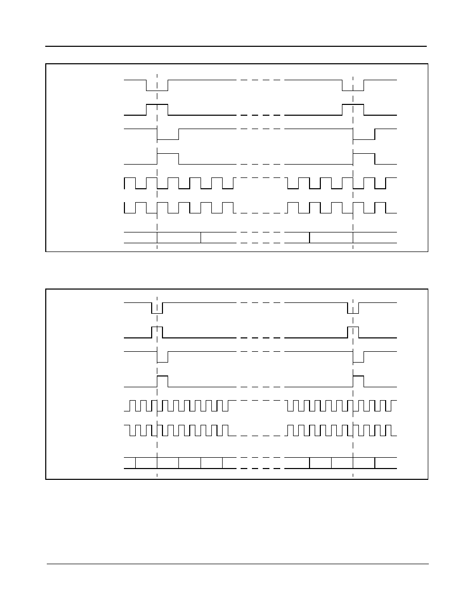
Figure 4 - Input Timing when CKIN1 - 0 bits = "10" in the CR
Figure 5 - Input Timing when CKIN1 - 0 bits = "01" in the CR
FPi (244 ns)
FPINP = 0
FPINPOS = 0
FPi (244 ns)
FPINP = 1
FPINPOS = 0
FPi (244 ns)
FPINP = 0
FPINPOS = 1
FPi (244 ns)
FPINP = 1
FPINPOS = 1
CKi
(4.096 MHz)
CKINP = 0
CKi
(4.096 MHz)
CKINP = 1
7
6
1
0
0
7
STi
(2.048 Mbps)
Channel 0
Channel 31
ST
-BUS
GC
I
-
Bu
s
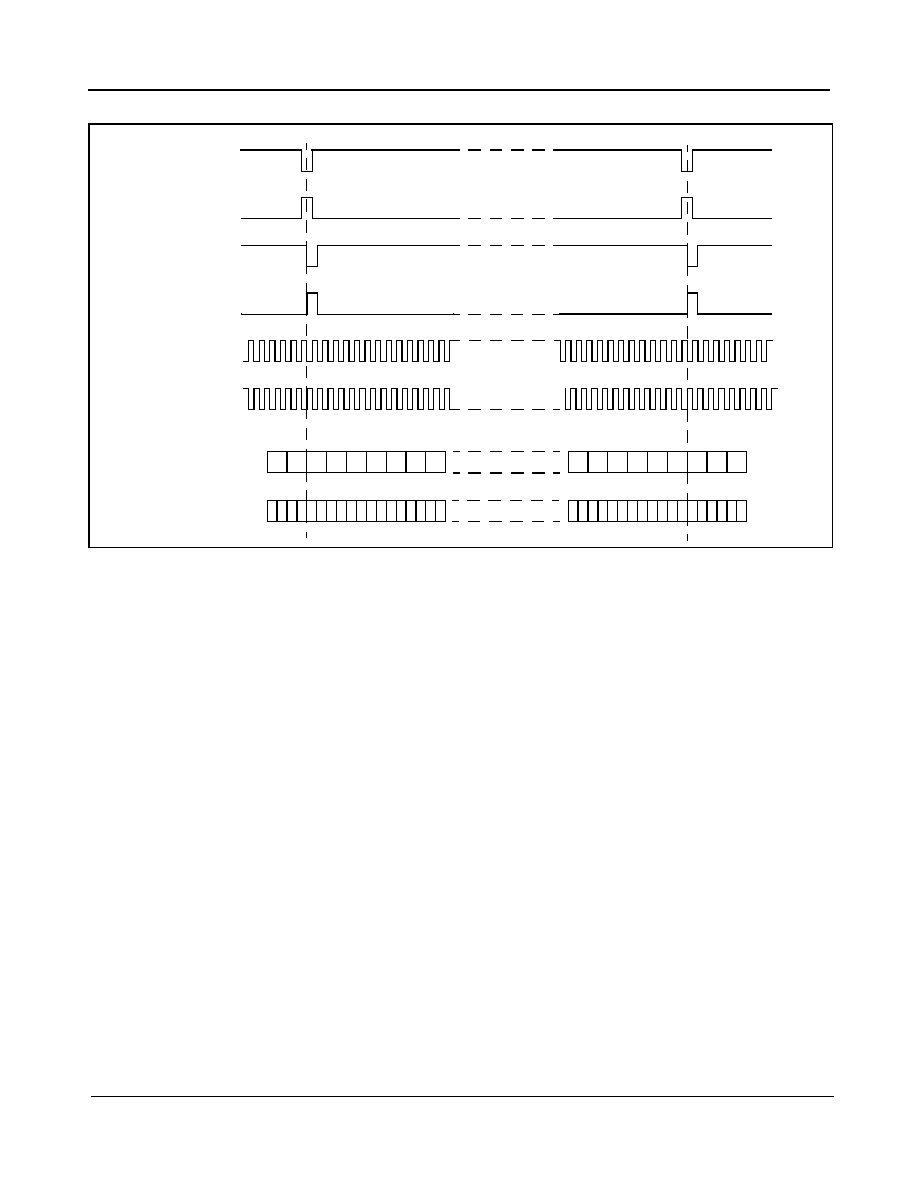
FPi (122 ns)
FPINP = 0
FPINPOS = 0
FPi (122 ns)
FPINP = 1
FPINPOS = 0
FPi (122 ns)
FPINP = 0
FPINPOS = 1
FPi (122 ns)
FPINP = 1
FPINPOS = 1
CKi
(8.192 MHz)
CKINP = 0
CKi
(8.192 MHz)
CKINP = 1
STi
(4.096 Mbps)
Channel 0
Channel 63
6
5
4
1
0
2
7
6
7
1
0
ST
-BUS
GC
I
-
Bu
s
ZL50015
Data Sheet
24
Zarlink Semiconductor Inc.
Figure 6 - Input Timing when CKIN1 - 0 = "00" in the CR
5.0 ST-BUS and GCI-Bus Timing
The ZL50015 is capable of operating using either the ST-BUS or GCI-Bus standards. The output timing that the
device generates is defined by the bus standard. In the ST-BUS standard, the output frame boundary is defined by
the falling edge of CKo while FPo is low. In the GCI-Bus standard, the frame boundary is defined by the rising edge
of CKo while FPo goes high. The data rates define the number of channels that are available in a 125
µs frame
pulse period.
By default, the ZL50015 is configured for ST-BUS input and output timing. To set the input timing to conform to the
GCI-Bus standard, FPINPOS (bit 9) and FPINP (bit 7) in the Control Register (CR) must be set. To set output timing
to conform to the GCI-Bus standard, FPO[n]P and FPO[n]POS must be set in the Output Clock and Frame Pulse
Selection Register (OCFSR). The CKO[n]P bits in the Output Clock and Frame Pulse Selection Register control the
polarity (positive-going or negative-going) of the output clocks.
6.0 Output Timing Generation
The ZL50015 generates frame pulse and clock timing. There are five output frame pulse pins (FPo0 - 3, 5) and six
output clock pins (CKo0 - 5). All output frame pulses are 8 kHz output signals. By default, the output frame
boundary is defined by the falling edge of the CKo0, while FPo0 is low. At the output frame boundary, the CKo1,
CKo2 and CKo3 output clocks will by default have a falling edge, while FPo1, FPo2 and FPo3 will be low. At the
output frame boundary, CKo4 will by default have a falling edge while FPo0 is low (CKo4 has no corresponding
output frame pulse). At the output frame boundary, CKo5 will by default have a rising edge while FPo5 (FPo_OFF2)
will be low. The duration of the frame pulse low cycle and the frequency of the corresponding output clock are
shown in Table 3 on page 25. Every frame pulse and clock output can be tristated by programming the enable bits
in the Internal Mode Selection (IMS) register.
FPi (61 ns)
FPINP = 0
FPINPOS = 0
FPi (61 ns)
FPINP = 1
FPINPOS = 0
FPi (61 ns)
FPINP = 0
FPINPOS = 1
FPi (61 ns)
FPINP = 1
FPINPOS = 1
CKi
(16.384 MHz)
CKINP = 0
CKi
(16.384 MHz)
CKINP = 1
STi
(8.192 Mbps)
Channel 0
Channel N = 127
6 5 4 3 2 1
3 2 1 0
5 4
7
6 5
7
1 0
STi
(16.384 Mbps)
Channel 0
Channel N = 255
6
7
4
5
2
3
0
1
6
7
4
5
2
3
2
3
0
1
6
7
4
5
2
3
6
7
4
5
2
3
0
1
2
3
0
1
ST
-B
US
GC
I
-
Bus

ZL50015
Data Sheet
25
Zarlink Semiconductor Inc.
The output timing is dependent on the operation mode that is selected. When the device is in Divided Slave mode,
the frequencies on CKo0 - 3 cannot be greater than the input clock, CKi. For example, if the input clock is
8.192 MHz, the CKo2 pin will not produce a valid output clock and the CKo3 pin can only be programmed to output
a 4.096 MHz or 8.192 MHz clock signal. The output clocks CKo4 - 5 will not generate valid outputs unless the
SLV_DPLLEN (bit 13) of the Control Register (CR) is set.
In Master mode there are programmable output frame pulse, FPo3, and clock pins, CKo3 and CKo4. The outputs
from FPo3 and CKo3 are programmed by the CKOFPO3SEL1 - 0 (bits 13 - 12) in the Output Clock and Frame
Pulse Selection (OCFSR) register. The output clock pin, CKo4, is controlled by setting the CKO4SEL (bit 14) in the
OCFSR register.
In Multiplied Slave mode, CKo4 and CKo5 are not available unless SLV_DPLLEN is set in the Control Register. All
other clocks and frame pulses correspond to the timing shown in Table 3 above.
The device also delivers positive or negative output frame pulse and ST-BUS/GCI-Bus output clock formats via the
programming of various bits in the Output Clock and Frame Pulse Selection Register (OCFSR). By default, the
device delivers the negative output clock format. The ZL50015 can also deliver GCI-Bus format output frame pulses
by programming bits of the Output Clock and Frame Pulse Selection Register (OCFSR). As there is a separate bit
setting for each frame pulse output, some of the outputs can be set to operate in ST-BUS mode and others in
GCI-Bus mode.
The following figures describe the usage of the FPO0P, FPO1P, FPO2P, FPO3P, CKO0P, CKO1P, CKO2P, CKO3P,
CKO4P and CKO5P bits to generate the FPo0 - 3 and CKo0 - 5 timing. FPo_OFF2 is configured to provide the
non-offset frame pulse corresponding to the 19.44 MHz clock on CKo5 by setting the FP19EN (bit 10) in the
FPOFF2 register. In this instance, FPo_OFF2 can be labeled as FPo5.
Pin Name
Output Timing Rate
Output Timing Unit
FPo0 pulse width
244
ns
CKo0
4.096
MHz
FPo1 pulse width
122
ns
CKo1
8.192
MHz
FPo2 pulse width
61
ns
CKo2
16.384
MHz
FPo3 pulse width
244, 122, 61 or 30
ns
CKo3
4.096, 8.192, 16.384 or 32.768
MHz
CKo4
1.544 or 2.048
MHz
FPo5 pulse width
51
ns
CKo5
19.44
MHz
Table 3 - Output Timing Generation
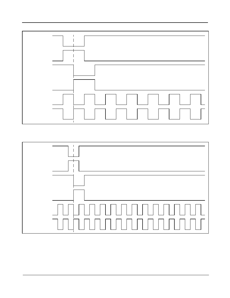
ZL50015
Data Sheet
26
Zarlink Semiconductor Inc.
Figure 7 - Output Timing for CKo0 and FPo0
Figure 8 - Output Timing for CKo1 and FPo1
CKOFPO0EN = 1
FPO0P = 0
FPO0POS = 0
CKOFPO0EN = 1
FPO0P = 1
FPO0POS = 0
CKOFPO0EN = 1
FPO0P = 0
FPO0POS = 1
CKOFPO0EN = 1
FPO0P = 1
FPO0POS = 1
CKOFPO0EN = 1
CKO0P = 0
CKo0 = 4.096 MHz
CKOFPO0EN = 1
CKO0P = 1
CKo0 = 4.096 MHz
ST
-BU
S
GC
I
-
Bu
s
CKOFPO1EN = 1
FPO1P = 0
FPO1POS = 0
CKOFPO1EN = 1
FPO1P = 1
FPO1POS = 0
CKOFPO1EN = 1
FPO1P = 0
FPO1POS = 1
CKOFPO1EN = 1
FPO1P = 1
FPO1POS = 1
CKOFPO1EN = 1
CKO1P = 0
CKo1 = 8.192 MHz
CKOFPO1EN = 1
CKO1P = 1
CKo1 = 8.192 MHz
ST
-BUS
GCI-
Bus
ZL50015
Data Sheet
27
Zarlink Semiconductor Inc.
Figure 9 - Output Timing for CKo2 and FPo2
Figure 10 - Output Timing for CKo3 and FPo3 with CKoFPo3SEL1-0="11"
CKOFPO2EN = 1
FPO2P = 0
FPO2POS = 0
CKOFPO2EN = 1
FPO2P = 1
FPO2POS = 0
CKOFPO2EN = 1
FPO2P = 0
FPO2POS = 1
CKOFPO2EN = 1
FPO2P = 1
FPO2POS = 1
CKOFPO2EN = 1
CKO2P = 0
CKo2 = 16.384 MHz
CKOFPO2EN = 1
CKO2P = 1
CKo2 = 16.384 MHz
ST
-BUS
GCI
-
Bu
s
CKOFPO3EN = 1
CKOFPO3SEL1-0 = 11
FPO3P = 0
FPO3POS = 0
CKOFPO3EN = 1
CKOFPO3SEL1-0 = 11
FPO3P = 1
FPO3POS = 0
CKOFPO3EN = 1
CKOFPO3SEL1-0 = 11
FPO3P = 0
FPO3POS = 1
CKOFPO3EN = 1
CKOFPO3SEL1-0 = 11
FPO3P = 1
FPO3POS = 1
CKOFPO3EN = 1
CKOFPO3SEL1-0 = 11
CKO3P = 0
CKo3 = 32.768 MHz
CKOFPO3EN = 1
CKOFPO3SEL1-0 = 11
CKO3P = 1
CKo3 = 32.768 MHz
NOTE:
When CKOFPO3SEL1-0 = "00," the output for FPo3 and CKo3 follow the same as Figure 7: Output Timing for CKo0 and FPo0
When CKOFPO3SEL1-0 = "01," the output for FPo3 and CKo3 follow the same as Figure 8: Output Timing for CKo1 and FPo1
When CKOFPO3SEL1-0 = "10," the output for FPo3 and CKo3 follow the same as Figure 9: Output Timing for CKo2 and FPo2
ST
-BUS
GC
I
-
Bu
s

ZL50015
Data Sheet
28
Zarlink Semiconductor Inc.
Figure 11 - Output Timing for CKo4
Figure 12 - Output Timing for CKo5 and FPo5 (FPo_OFF2)
CKOFPO0EN = 1
FPO0P = 0
FPO0POS = 0
CKOFPO0EN = 1
FPO0P = 1
FPO0POS = 0
CKOFPO0EN = 1
FPO0P = 0
FPO0POS = 1
CKOFPO0EN = 1
FPO0P = 1
FPO0POS = 1
CKO4EN = 1
CKO4P = 1
CKO4SEL = 0
CKo4 = 2.048 MHz
CKOFPO4EN = 1
CKO4P = 0
CKO4SEL = 0
CKo4 = 2.048 MHz
CKO4EN = 1
CKO4P = 1
CKO4SEL = 1
CKo4 = 1.544 MHz
CKOFPO4EN = 1
CKO4P = 0
CKO4SEL = 1
CKo4 = 1.544 MHz
Note:
While there is no frame pulse output directly tied to the CKo4, the output clocks are based on the frame pulse generated by FPo0
ST
-BUS
GCI-
Bus
FPo5 (FPo_OFF2)
FP19EN = 1
CKO5EN = 1
CK5 = 19.44 MHz
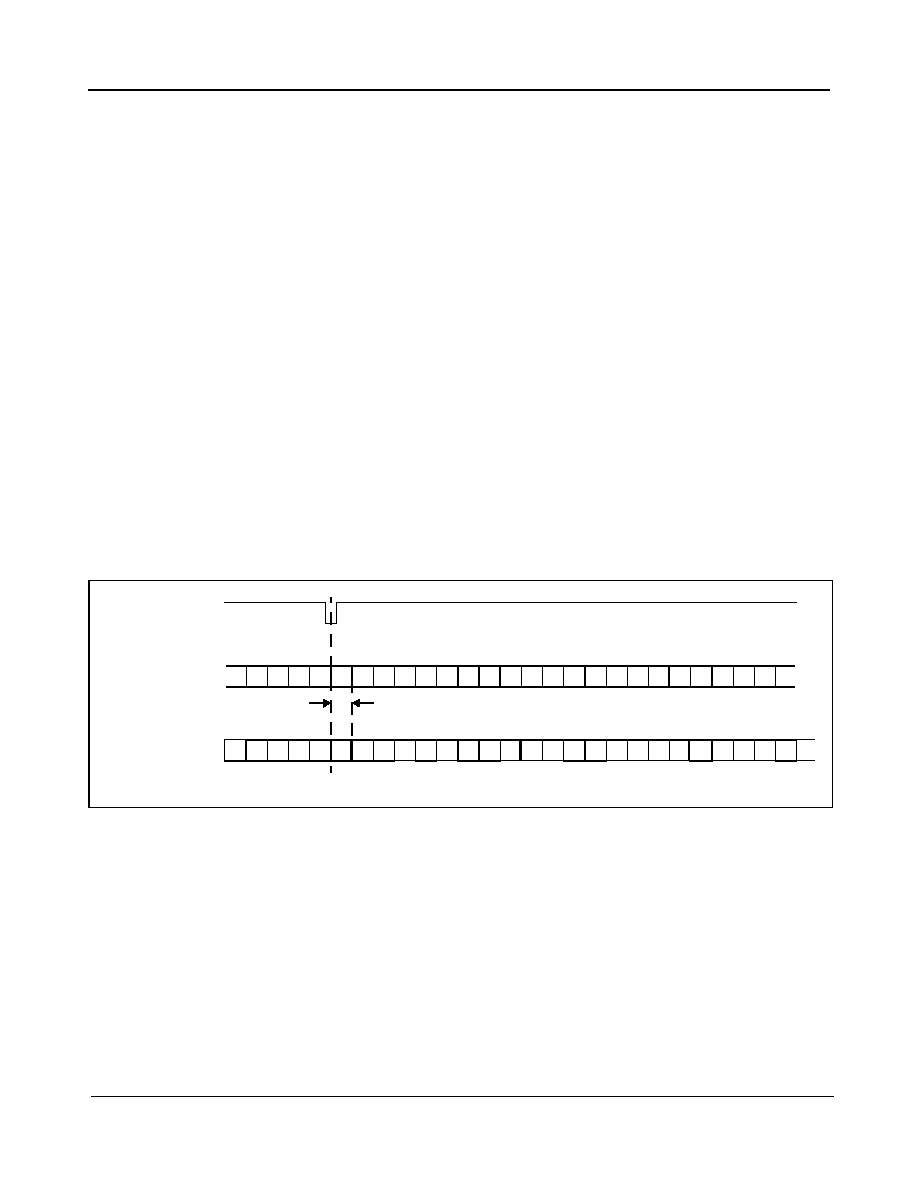
ZL50015
Data Sheet
29
Zarlink Semiconductor Inc.
7.0 Data Input Delay and Data Output Advancement
Various registers are provided to adjust the input delay and output advancement for each input and output data
stream. The input bit delay and output bit advancement can vary from 0 to 7 bits for each individual stream.
If input delay of less than a bit is desired, different sampling points can be used to handle the adjustments. The
sampling point can vary from 1/4 to 4/4 with a 1/4-bit increment for all input streams, unless the stream is operating
at 16.384 Mbps, in which case the fractional bit delay has a 1/2-bit increment. By default, the sampling point is set
to the 3/4-bit location for non-16.384 Mbps data rates and the 1/2-bit location for the 16.384 Mbps data rate.
The fractional output bit advancement can vary from 0 to 3/4 bits, again with a 1/4-bit increment, unless the output
stream is operating at 16.384 Mbps, in which case the output bit advancement has a 1/2-bit increment from 0 to 1/2
bit. By default, there is 0 output bit advancement.
Although input delay or output advancement features are available on streams which are operating in bi-directional
mode it is not recommended, as it can easily cause bus contention. If users require this function, special attention
must be given to the timing to ensure contention is minimized.
7.1 Input Bit Delay Programming
The input bit delay programming feature provides users with the flexibility of handling different wire delays when
designing with source streams for different devices.
By default, all input streams have zero bit delay, such that bit 7 is the first bit that appears after the input frame
boundary (assuming ST-BUS formatting). The input delay is enabled by STIN[n]BD2-0 (bits 8 - 6) in the Stream
Input Control Register 0 - 15 (SICR0 - 15) as described in Table 43 on page 79. The input bit delay can range from
0 to 7 bits.
Figure 13 - Input Bit Delay Timing Diagram (ST-BUS)
FPi
STi[n]
Bit Delay = 0
(Default)
Channel 0
7
Channel 1
6 5 4 3 2 1 0 7 6 5 4 3 2 1 0 7 6 5 4 3 2
Channel 2
2 1 0
4 3
Last Channel
STi[n]
Bit Delay = 1
Channel 0
7
Channel 1
6 5 4 3 2 1 0 7 6 5 4 3 2 1 0 7 6 5 4 3
Channel 2
2 1 0
4 3
Last Channel
Bit Delay = 1
5
Note: Last Channel = 31, 63, 127 and 255 for 2.048, 4.096, 8.192 and 16.384 Mbps modes respectively.
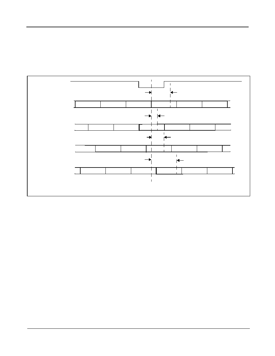
ZL50015
Data Sheet
30
Zarlink Semiconductor Inc.
7.2 Input Bit Sampling Point Programming
In addition to the input bit delay feature, the ZL50015 allows users to change the sampling point of the input bit by
programming STIN[n]SMP 1-0 (bits 5 - 4) in the Stream Input Control Register 0 - 15 (SICR0 - 15). For input
streams operating at any rate except 16.384 Mbps, the default sampling point is at 3/4 bit and users can change the
sampling point to 1/4, 1/2, 3/4 or 4/4 bit position. When the stream is operating at 16.384 Mbps, the default
sampling point is 1/2 bit and can be adjusted to a 4/4 bit position.
Figure 14 - Input Bit Sampling Point Programming
FPi
STi[n]
STIN[n]SMP1-0 = 01
(2, 4 or 8 Mbps)
Channel 0
Last Channel
Sampling Point = 1/4 Bit
STi[n]
STIN[n]SMP1-0 = 10
(2, 4 or 8 Mbps)
STIN[n]SMP1-0 = 00
(16 Mbps - Default)
Channel 0
Last Channel
Sampling Point = 1/2 Bit
STi[n]
STIN[n]SMP1-0 = 00
(2, 4 or 8 Mbps -
Default)
Channel 0
Last Channel
Sampling Point = 3/4 Bit
1
0
7
6
2
Note: Last Channel = 31, 63, 127 and 255 for 2.048, 4.096, 8.192 and 16.384 Mbps mode respectively
STi[n]
STIN[n]SMP1-0 = 11
(2, 4 or 8 Mbps)
STIN[n]SMP1-0 = 10
(16 Mbps)
Channel 0
Last Channel
Sampling Point = 4/4 Bit
5
1
0
7
6
5
1
0
7
6
5
1
0
7
6
2
5

ZL50015
Data Sheet
31
Zarlink Semiconductor Inc.
The input delay is controlled by STIN[n]BD2-0 (bits 8 - 6) to control the bit shift and STIN[n]SMP1 - 0 (bits 5 - 4) to
control the sampling point in the Stream Input Control Register 0 - 15 (SICR0 - 15).
Figure 15 - Input Bit Delay and Factional Sampling Point
7.3 Output Advancement Programming
This feature is used to advance the output data of individual output streams with respect to the output frame
boundary. Each output stream has its own bit advancement value which can be programmed in the Stream Output
Control Register 0 - 15 (SOCR0 - 15).
By default, all output streams have zero bit advancement such that bit 7 is the first bit that appears after the output
frame boundary (assuming ST-BUS formatting). The output advancement is enabled by STO[n]AD 2 - 0 (bits 6 - 4)
of the Stream Output Control Register 0 - 15 (SOCR0 - 15) as described in Table 45 on page 83. The output bit
advancement can vary from 0 to 7 bits.
Nominal Channel n+1 Boundary
7
6
5
4
3
2
1
0
7
0
000 01
000 10
000 00 (Default)
000 11
001 01
001 10
001 00
001 11
010 01
010 10
010 00
010 11
011 01
011 10
011 00
011 11
111 00
111 10
111 01
110 11
110 00
110 10
110 01
101 11
101 00
101 10
101 01
100 11
100 00
100 10
100 01
111 11
The first 3 bits represent STIN[n]BD2 - 0 for setting the bit delay
The second set of 2 bits represent STIN[n]SMP1 - 0 for setting the sampling point offset
STi[n]
Nominal Channel n Boundary
Example: With a setting of 011 10 the offset will be 3 bits at a 1/2 sampling point
Note: Italic settings can be used in 16 Mbps mode (1/2 and 4/4 sampling point)
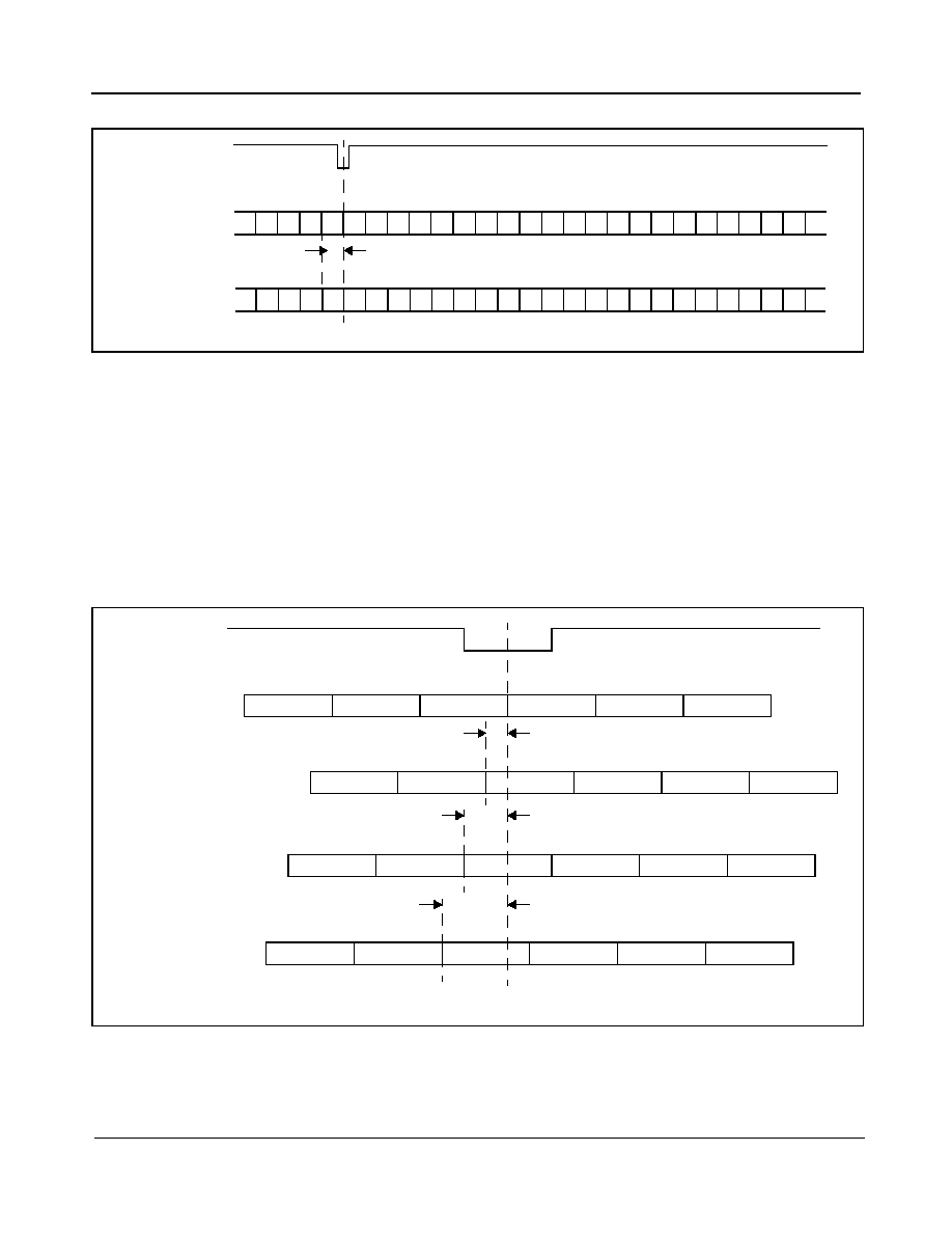
ZL50015
Data Sheet
32
Zarlink Semiconductor Inc.
Figure 16 - Output Bit Advancement Timing Diagram (ST-BUS)
7.4 Fractional Output Bit Advancement Programming
In addition to the output bit advancement, the device has a fractional output bit advancement feature that offers
better resolution. The fractional output bit advancement is useful in compensating for varying parasitic load on the
serial data output pins.
By default all of the streams have zero fractional bit advancement such that bit 7 is the first bit that appears after the
output frame boundary. The fractional output bit advancement is enabled by STO[n]FA 1 - 0 (bits 8 - 7) in the
Stream Output Control Register 0 - 15 (SOCR0 - 15). For all streams running at any data rate except 16.384 Mbps
the fractional bit advancement can vary from 0, 1/4, 1/2 to 3/4 bits. For streams operating at 16.384 Mbps, the
fractional bit advancement can be set to either 0 or 1/2 bit.
Figure 17 - Output Fractional Bit Advancement Timing Diagram (ST-BUS)
FPi
STio[n]
Bit Adv = 0
(Default)
Channel 0
7
Channel 1
6 5 4 3 2 1 0 7 6 5 4 3 2 1 0 7 6 5 4 3 2
Channel 2
2 1 0
4 3
Last Channel
STio[n]
Bit Adv = 1
Channel 0
7
Channel 1
6 5 4 3 2 1 0 7 6 5 4 3 2 1 0 7 6 5 4 3
Channel 2
2 1 0
3
Last Channel
Bit Advancement = 1
Note: Last Channel = 31, 63, 127 and 255 for 2.048, 4.096, 8.192 and 16.384 Mbps modes respectively.
2 1
FPi
STio[n]
STo[n]FA1-0 = 00
(Default 2, 4, 8 or
16Mbps)
Channel 0
7
Last Channel
STio[n]
STo[n]FA1-0 = 01
(2, 4 or 8 Mbps)
Channel 0
Last Channel
Fractional Bit Advancement = 1/4 Bit
6
5
2
1
0
STio[n]
STo[n]FA1-0 = 10
(2, 4 or 8Mbps)
STo[n]FA1-0 = 01
(16 Mbps)
Channel 0
Last Channel
Fractional Bit Advancement = 1/2 Bit
STio[n]
STo[n]FA1-0 = 11
(2, 4 or 8 Mbps)
Channel 0
Last Channel
Fractional Bit Advancement = 3/4 Bit
Note: Last Channel = 31, 63, 127 and 255 for 2.048, 4.096, 8.192 and 16.384 Mbps modes respectively.
7
6
5
1
0
7
6
5
1
0
7
6
5
1
0
4
4
4
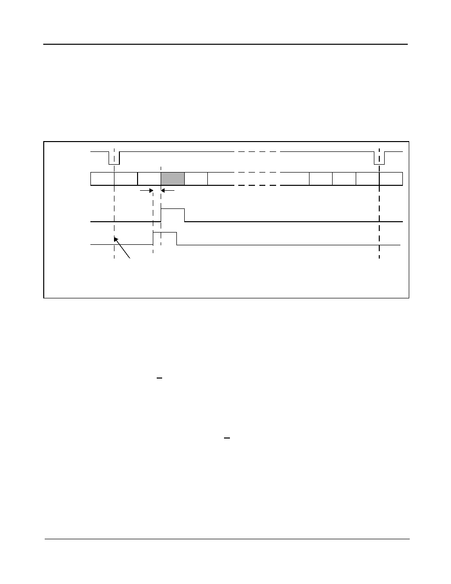
ZL50015
Data Sheet
33
Zarlink Semiconductor Inc.
7.5 External High Impedance Control Advancement
The external high impedance signals can be programmed to better match the timing required by the external
buffers. By default, the output timing of the STOHZ signals follows the programmed channel delay and bit offset of
their corresponding ST-BUS/GCI-Bus output streams. In addition, for all high impedance streams operating at any
data rate except 16.384 Mbps, the user can advance the STOHZ signals a further 0, 1/4, 1/2, 3/4 or 4/4 bits by
programming STOHZ[n]A 2 - 0 (bit 11 - 9) in the Stream Output Control Register. When the stream is operating at
16.384 Mbps, the additional STOHZ advancement can be set to 0, 1/2 or 4/4 bits by programming the same
register.
Figure 18 - Channel Switching External High Impedance Control Timing
8.0 Data Delay Through the Switching Paths
The switching of information from the input serial streams to the output serial streams results in a throughput delay.
The device can be programmed to perform timeslot interchange functions with different throughput delay
capabilities on a per-channel basis. For voice applications, select variable throughput delay to ensure minimum
delay between input and output data. In wideband data applications, select constant delay to maintain the frame
integrity of the information through the switch. The delay through the device varies according to the type of
throughput delay selected by the V/C (bit 14) in the Connection Memory Low when CMM = 0.
8.1 Variable Delay Mode
Variable delay mode causes the output channel to be transmitted as soon as possible. This is a useful mode for
voice applications where the minimum throughput delay is more important than frame integrity. The delay through
the switch can vary from 7 channels to 1 frame + 7 channels. To set the device into variable delay mode, VAREN
(bit 4) in the Control Register (CR) must be set before V/C (bit 14) in the Connection Memory Low when CMM = 0.
If the VAREN bit is not set and the device is programmed for variable delay mode, the information read on the
output stream will not be valid.
CH0
CH1
CH2
CH3
Last-2
Last-1
Last
CH0
Last
HiZ
FPi
STio[n]
STOHZ[n]
STOHZ[n]
(with Advancement)
(Default = No Advancement)
STOHZ Advancement (Programmable in 4 steps of 1/4 bit
for 2.048 Mbps, 4.096 Mbps and 8.192 Mbps
Programmable in 2 steps of 1/2 bit for 16.384 Mbps)
Note: n = 0 to 7
Note: Last = Last Channel of 31, 63, 127 and 255 for 2.048 Mbps, 4.096 Mbps. 8.192 Mbps and 16.384 Mbps modes respectively.
Output Frame Boundary
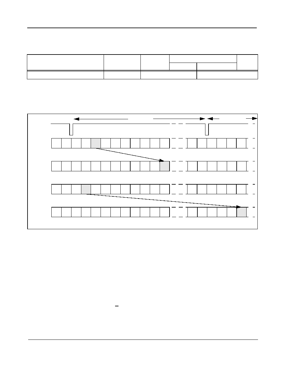
ZL50015
Data Sheet
34
Zarlink Semiconductor Inc.
In variable delay mode, the delay depends on the combination of the source and destination channels of the input
and output streams.
For example, if Stream 4 Channel 2 is switched to Stream 5 Channel 9 with variable delay, the data will be output in
the same 125
µs frame. Contrarily, if Stream 6 Channel 1 is switched to Stream 9 Channel 3, the information will
appear in the following frame.
Figure 19 - Data Throughput Delay for Variable Delay
8.2 Constant Delay Mode
In this mode, frame integrity is maintained in all switching configurations. The delay though the switch is 2 frames -
Input Channel + Output Channel. This can result in a minimum of 1 frame + 1 channel delay if the last channel on a
stream is switched to the first channel of a stream. The maximum delay is 3 frames - 1 channel. This occurs when
the first channel of a stream is switched to the last channel of a stream. The constant delay mode is available for all
output channels.
The data throughput delay is expressed as a function of ST-BUS/GCI-Bus frames, input channel number (m) and
output channel number (n). The data throughput delay (T) is:
T = 2 frames + (n - m)
The constant delay mode is controlled by V/C (bit 14) in the Connection Memory Low when CMM = 0. When this bit
is set low, the channel is in constant delay mode. If VAREN (bit 4) in the Control Register (CR) is set (to enable
variable throughput delay on a chip-wide basis), the device can still be programmed to operate in constant delay
mode.
m = input channel number
n = output channel number
n-m <= 0
0 < n-m < 7
n-m = 7
n-m > 7
STio < STi
STio >= STi
T = Delay between input and output
1 frame - (m-n)
1 frame + (n-m)
n-m
Table 4 - Delay for Variable Delay Mode
L-2
L-1 CH0 CH1 CH2 CH3
L-2
L-1 CH0 CH1 CH2 CH3
L-2
L-1 CH0 CH1 CH2 CH3
L-2
L-1 CH0 CH1 CH2 CH3
L-2
L-1 CH0 CH1 CH2 CH3
L-2
L-1 CH0 CH1 CH2 CH3
L-2
L-1 CH0 CH1 CH2 CH3
L-2
L-1 CH0 CH1 CH2 CH3
CH4 CH5 CH6
CH4 CH5 CH6
CH4 CH5 CH6
CH4 CH5 CH6
CH7 CH8 CH9
CH7 CH8 CH9
CH7 CH8 CH9
CH7 CH8 CH9
STi4
CH2
STio5
CH9
STi6
CH1
STio9
CH3
Frame N
Frame N + 1
L = last channel = 31, 63, 127, or 255 for 2.048 Mbps, 4.096 Mbps
,
8.192 Mbps, or 16.384 Mbps respectively.

ZL50015
Data Sheet
35
Zarlink Semiconductor Inc.
Figure 20 - Data Throughput Delay for Constant Delay
9.0 Connection Memory Description
The connection memory consists of two blocks, Connection Memory Low (CM_L) and Connection Memory High
(CM_H). The CM_L is 16 bits wide and is used for channel switching and other special modes. The CM_H is 5 bits
wide and is used for the voice coding function. When UAEN (bit 15) of the Connection Memory Low (CM_L) is low,
µ-law/A-law conversion will be turned off and the contents of CM_H will be ignored. Each connection memory
location of the CM_L or CM_H can be read or written via the 16 bit microprocessor port within one microprocessor
access cycle. See Table 50 on page 86 for the address mapping of the connection memory. Any unused bits will be
reset to zero on the 16-bit data bus.
For the normal channel switching operation, CMM (bit 0) of the Connection Memory Low (CM_L) is programmed
low. SCA7 - 0 (bits 8 - 1) indicate the source (input) channel address and SSA4 - 0 (bits 13 - 9) indicate the source
(input) stream address. The 5-bit contents of the CM_H will be ignored during the normal channel switching mode
without the
µ-law/A-law conversion when UAEN (bit 15) of the Connection Memory Low (CM_L) is set to zero. If
µ-law/A-law conversion is required, the CM_H bits must be programmed first to provide the voice/data information,
the input coding law and the output coding law before the assertion of UAEN (bit 15) in the Connection Memory
Low.
When CMM (bit 0) of the Connection Memory Low (CM_L) is programmed high, the ZL50015 will operate in one of
the special modes described in Table 52 on page 88. When the per-channel message mode is enabled, MSG7 - 0
(bit 10 - 3) in the Connection Memory Low (CM_L) will be output via the serial data stream as message output data.
When the per-channel message mode is enabled, the
µ-law/A-law conversion can also be enabled as required.
L-2
L-1 CH0 CH1 CH2 CH3
L-2
L-1 CH0 CH1 CH2 CH3
L-2
L-1 CH0 CH1 CH2 CH3
L-2
L-1 CH0 CH1 CH2 CH3
L-2
L-1 CH0 CH1 CH2 CH3
L-2
L-1 CH0 CH1 CH2 CH3
L-2
L-1 CH0 CH1 CH2 CH3
L-2
L-1 CH0 CH1 CH2 CH3
L-2
L-1 CH0 CH1 CH2 CH3
L-2
L-1 CH0 CH1 CH2 CH3
L-2
L-1 CH0 CH1 CH2 CH3
L-2
L-1 CH0 CH1 CH2 CH3
STi
STio
STi
STio
L = last channel = 31, 63, 127, or 255 for 2.048 Mbps, 4.096 Mbps
,
8.192 Mbps, or 16.384 Mbps respectively
Frame N
Frame N + 1
Frame N + 2
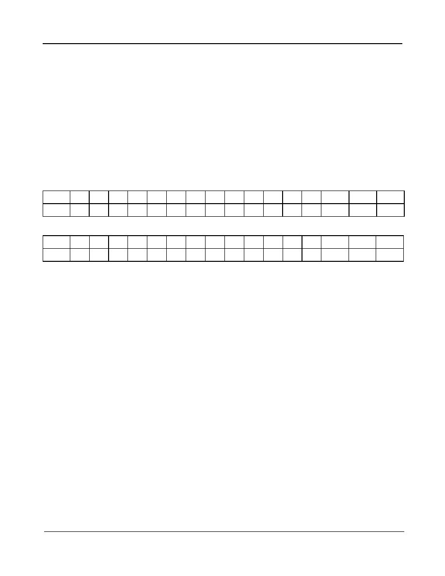
ZL50015
Data Sheet
36
Zarlink Semiconductor Inc.
10.0 Connection Memory Block Programming
This feature allows for fast initialization of the connection memory after power up.
10.1 Memory Block Programming Procedure
1. Set MBPE (bit 3) in the Control Register (CR) from low to high.
2. Configure BPD2 - 0 (bits 3 - 1) in the Internal Mode Selection (IMS) register to the desired values to be loaded
into CM_L.
3. Start the block programming by setting MBPS (bit 0) in the Internal Mode Selection Register (IMS) high. The val-
ues stored in BPD2 - 0 will be loaded into bits 2 - 0 of all CM_L positions. The remaining CM_L locations (bits 15
- 3) and the programmable values in the CM_H (bits 4 - 0) will be loaded with zero values.
The following tables show the resulting values that are in the CM_L and CM_H connection memory locations.
Note: Bits 15 to 5 are reserved in Connection Memory High and should always be 0.
It takes at least two frame periods (250
µs) to complete a block program cycle.
MBPS (bit 0) in the Control Register (CR) will automatically reset to a low position after the block programming
process has completed.
MBPE (bit 3) in the Internal Mode Selection (IMS) register must be cleared from high to low to terminate the block
programming process. This is not an automatic action taken by the device and must be performed manually.
Note: Once the block program has been initiated, it can be terminated at any time prior to completion by setting
MBPS (bit 0) in the Control Register (CR) or MBPE (bit 3) in the Internal Mode Selection (IMS) register to low. If the
MBPE bit was used to terminate the block programming, the MBPS bit will have to be set low before enabling other
device operations.
11.0 Device Operation in Master Mode and Slave Modes
This device has two main operating modes - Master mode and Slave mode. Each operating mode has different
input/output clock and frame pulse setup requirements and usage.
If the device is programmed to work in Master mode, it is expected that the input clock and frame pulse will be
supplied from the embedded DPLL, either directly using the internal loopback mode or indirectly through external
loopback path. Sources and destinations of the device's serial input and output data, respectively, have to be
synchronized with the device's output clock and frame pulse. In Master mode, output clocks and frame pulses are
driven by the DPLL and they are always available with any of the specified frequencies.
The device can also operate in two different Slave modes: Divided Slave mode and Multiplied Slave mode. In either
Slave modes, output clocks and frame pulses are generated based on CKi and FPi. The difference is that, in
Divided Slave mode, the output clocks and frame pulses are directly divided from CKi/FPi, while in Multiplied Slave
mode, the output clocks and frame pulses are generated from an internal high-speed clock synchronized to CKi
Bit
15
14
13
12
11
10
9
8
7
6
5
4
3
2
1
0
Value
0
0
0
0
0
0
0
0
0
0
0
0
0
BPD2
BPD1
BPD0
Table 5 - Connection Memory Low After Block Programming
Bit
15
14
13
12
11
10
9
8
7
6
5
4
3
2
1
0
Value
0
0
0
0
0
0
0
0
0
0
0
0
0
0
0
0
Table 6 - Connection Memory High After Block Programming

ZL50015
Data Sheet
37
Zarlink Semiconductor Inc.
and FPi. Therefore, in Divided Slave mode, the output clock rates cannot exceed the CKi rate (the output data rates
are also limited as per Table 1, but in Multiplied Slave mode, all specified output clock rates and data rates are
available on CKo0-3 and STio0-15. The input data rate cannot exceed the CKi rate in either Slave modes, because
input data are always sampled directly by CKi.
By default, CKo4, CKo5 and FPo5 are not available in Slave mode, as the embedded DPLL is disabled. However,
the DPLL can be activated even in Slave mode by programming the SLV DPLLEN bit in the Control Register. When
the DPLL is enabled in Slave mode, CKo4, CKo5 and FPo5 are generated from the DPLL synchronized to one of
the REF0-3 inputs, while the other clocks, frame pulses, and input/output data are synchronized to CKi/FPi. It
basically creates two separate timing domains - one for the DPLL, and one for data switch logic. The two can be
totally asynchronous to each other. In this case the DPLL will be fully functional, including its capability of reference
monitoring.
Note that an external oscillator is required whenever the DPLL is used.
Table 7, "ZL50015 Operating Modes" on page 37 summarizes the different modes of operation available within the
ZL50015. Each Major mode has various associated Minor modes that are determined by setting the relevant Input
Control pins and Control Register bits (Table 17, "Control Register (CR) Bits" on page 53) indicated in the table.
11.1 Master Mode Operation
When the device is in Master mode, the DPLL is phase-locked to the one of four DPLL reference signals, REF0 to
REF3, which are sourced by an external 8 kHz, 1.544 MHz, 2.048 MHz, 4.096 MHz, 8.192 MHz, 16.384 MHz or
19.44 MHz signal. The on-chip DPLL also offers reference switching and monitoring, jitter attenuation, freerun and
holdover functions. In this mode, STio0 - 15 are driven by a clock generated by the DPLL, which also provides all
the output clocks (CKo0 - 5) and frame pulses (FPo0 - 3 and FPo_OFF0 - 2). One of the output clocks and frame
pulses should be looped back to CKi/FPi as reference for the input data, either by internal loopback (by setting the
CKi_LP bit high in the Control Register) or through some external loopback paths. If external loopback is used, it is
recommended that CKo2 (16.384MHz) and FPo2 (61ns pulse) are used so that all input data rates are available.
Device
Input Pins
CR Register
Output Clock Pins
Data Pins
Operating Mode
Control
Signal
Bits
Reference Lock
Enabled
Clock Source
Major
Minor
OSC_EN MODE_4M
[1:0]
OSCi
CKi
OPM
[1:0]
SLV_DPLLEN CKi_LP
CKo0-3
CKo4-5 CKo0-3 CKo4-5
STi
STo
Master
CKi
1
00
20 MHz 4/8/16 M
00
X
0
Freerun, Holdover
or REF0-3
Yes
Yes
CKi*
Cko2
(DPLL)
Loopback
X
1
Cko2
Divided
Slave
4 M
1
11
20 MHz
4 M
01
1
X
CKi
REF0-3
Yes
CKi
CKo0-3
(CKi)
8/16 M
00
8/16 M
4 M
0
11
X
4 M
X0
0
X
No
8/16 M
00
8/16 M
Multiplied
Slave
4 M
1
11
20 MHz
4 M
11
1
CKi MULT REF0-3
Yes
CKo0-3
(CKi MULT)
8/16 M
00
8/16 M
4 M
0
11
X
4 M
X1
0
X
No
8/16 M
00
8/16 M
Legend:
X - Don't care or not applicable.
Reference Lock - Refers to what signal the output pins are locked to:
REF0-3 = Normal Mode
Cki = Bypass. Cki is passed directly through to CKo0-3.
Cki MULT = Cki is passed through clock multiplier to CKo0-3.
* CKi must be phase aligned (edge synchronous) to CKo0-3.
Clock Source - Refers to which clock samples STi and which clock outputs STo; STi applies when STi or STio is input; STo applies when STio is output.
Table 7 - ZL50015 Operating Modes

ZL50015
Data Sheet
38
Zarlink Semiconductor Inc.
11.2 Divided Slave Mode Operation
When the device is in Divided Slave mode, STio0 - 15 are driven by CKi. In this mode, the output streams and
clocks have the same jitter characteristics as the input clock (CKi), but the input and output data rates cannot
exceed the limit defined by CKi (as per Table 1). For example, if CKi is 4.096 MHz, the input and output data rate
cannot be higher than 2.048 Mbps, and the generated output clock rates cannot exceed 4.096 MHz. If the DPLL is
not enabled, an external oscillator is optional in Divided Slave mode.
11.3 Multiplied Slave Mode Operation
When the device is in Multiplied Slave mode, device hardware is used to multiply CKi internally. STio0 - 15 are
driven by this internally generated clock. In this mode, the output clocks and data can run at any of the specified
rates, but they may have different jitter characteristics from the input clock (CKi). The input data rates are still
limited by the CKi rate (as per Table 1), as input data are always sampled directly by CKi. If the DPLL is not
enabled, an external oscillator is not required in Multiplied Slave mode.
12.0 Overall Operation of the DPLL
The DPLL accepts four input references and delivers six output clocks and five output frame pulses. The DPLL
meets or exceeds all of the requirements of the Telcordia GR-1244-CORE standard for a Stratum 4E compliant
PLL. This includes the freerun, reference switching and monitoring, jitter/wander attenuation and holdover
functions. The intrinsic output jitter of the DPLL does not exceed 1.0 ns (except for the 1.544 MHz output).
The DPLL is able to lock to an input reference presented on the REF0 - 3 inputs. It is possible to force the DPLL
module to lock to a selected reference, to prefer one reference, to enter holdover mode or to freerun.
12.1 DPLL Timing Modes
There are four functional modes for the DPLL: normal, holdover, automatic and freerun modes. In addition to these
four functional modes, the DPLL can also be programmed to internal reset mode.
12.1.1 Normal Mode
In normal mode, the DPLL generates clocks and frame pulses that are phase locked to the active input reference.
Jitter on the input clock is attenuated by the DPLL.
12.1.2 Holdover Mode
In holdover mode, the DPLL no longer synchronizes the output clock to any input reference. It maintains the
frequency that it was at prior to entering holdover mode. The holdover mode typically happens when the input clock
becomes unreliable or is lost altogether. It takes some time for the system to realize that the input clock is
unreliable. Meanwhile, the DPLL tracks an unreliable clock. Therefore the DPLL could hold to an invalid frequency
when it enters holdover mode. In order to prevent this situation, the DPLL stores the current frequency at regular
intervals in holdover memory so that it can restore the frequency of the input clock just after the input clock became
unreliable.
12.1.3 Automatic Mode
In this mode, the state machine controls the DPLL based on the settings in the registers and the quality of the
reference input clocks. The DPLL is internally either in normal or in holdover mode. In the following two sections,
the reference selection and state machine operation in automatic mode will be explained in more details.
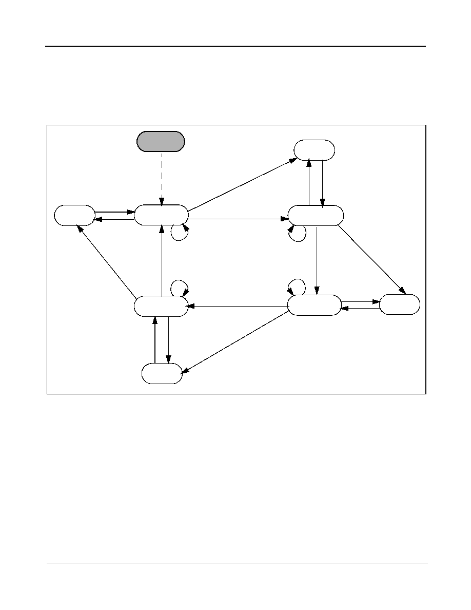
ZL50015
Data Sheet
39
Zarlink Semiconductor Inc.
12.1.3.1 Automatic Reference Switching Without Preferences
When the DPLL is programmed to operate in Automatic mode without Preference (RCCR Register, PMS2-0 bits =
000), all references, REF0-3, will have equal importance. A circulating Round Robin selection sequence
determines the reference to be used as shown in Figure 21. The state machine basically searches for valid
reference in a circular order of REF0 -> REF1 -> REF2 -> REF3 -> REF0, etc.
Figure 21 - No Preferred Reference (Round Robin) with Ref 0-3 available
Free run
Holdover 0
Holdover 1
Ref 0
Ref 1
Ref 3
Ref 2
Holdover 2
Holdover 3
All Ref failed
Ref 0 valid
Ref 0 failed
All Ref failed
All Ref failed
All Ref failed
Ref 1
valid
Ref 1
failed
Ref 2 valid
Re
f 3
va
lid
Ref 2 failed
Ref 3 failed
Re
f 2
v
alid
a
nd
Re
f 1
fa
ile
d
R
ef
0 v
alid
a
nd
R
ef
3 f
aile
d
Re
f 1
va
lid
an
d R
ef
0 f
aile
d
Re
f 3
va
lid
an
d R
ef
2 f
ail
ed
Start
Ref 1
and 2 fai
l
ed
a
nd (Re
f
3 or Ref 0
va
l
i
d
)
Ref 2 and 3 failed
and (Ref 0 or Ref 1 valid)
Ref 3 and 0 failed a
nd (Ref 1 or Ref 1
val
i
d)
Ref 0 and 1 failed
and (Ref 2 or Ref 3 valid)
ZL50015
Data Sheet
40
Zarlink Semiconductor Inc.
12.1.3.2 Automatic Reference Switching With Preferences
If a particular reference needs to have higher priority than the others, the device can be programmed in Automatic
mode with a preferred reference (RCCR Register, PMS2-0 bits = 001). When a preferred reference is selected, the
device can only switch automatically between two references, as shown in Table 8. The preferred reference will be
used as the primary reference and, by default, only its next consecutive reference will be used as the secondary
reference. No more than two references can be used in Automatic mode when a preferred reference is selected.
Figure 22 shows the state diagram for the four valid options of automatic reference switching with a preferred
reference.
Primary Reference (Preferred)
Secondary Reference
Option 1
Ref 0
Ref 1
Option 2
Ref 1
Ref 2
Option 3
Ref 2
Ref 3
Option 4
Ref 3
Ref 0
Table 8 - Preferred Reference Selection Options
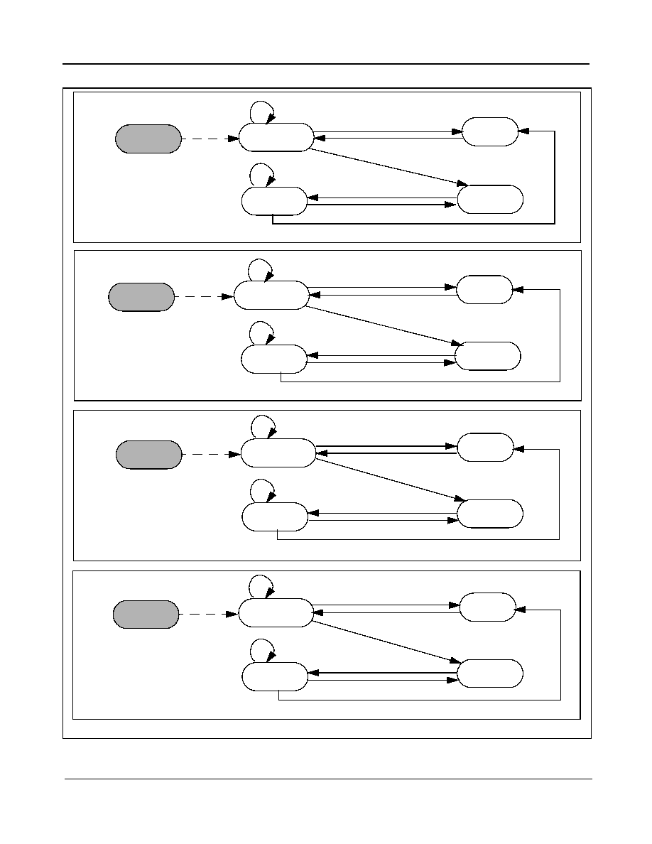
ZL50015
Data Sheet
41
Zarlink Semiconductor Inc.
Figure 22 - Automatic Reference Switching State Diagrams with Preferred Reference
Free run
Holdover 0
Ref 0
Ref 1
Holdover 1
Ref 1 valid
and Ref 0
failed
Ref 1 failed or Ref 0 valid
Ref 1 valid
Ref 0 valid
Preferred References :
Ref 0
Ref 0 valid
and Ref 0 failed
Note : other combinations not shown here are invalid settings and should not be used
DPLL will switch between
Ref 0 and Ref 1
Ref 0 failed
Ref 0 and 1 failed
Ref 0 and 1 failed
Free run
Holdover 2
Ref 2
Ref 3
Holdover 3
Ref 3 vali
d and Re
f 2 failed
Ref 3 failed or Ref 2 valid
Ref 3 valid
Ref 2 valid
Preferred References :
Ref 2
Ref 2 valid
and Ref 2 failed
DPLL will switch between
Ref 2 and Ref 3
Ref 2 failed
Ref 2 and 3 failed
Ref 2 and 3 failed
Free run
Holdover 1
Ref 1
Ref 2
Holdover 2
Ref 2 valid
and Ref 1
failed
Ref 2 failed or Ref 1 valid
Ref 2 valid
Ref 1 valid
Preferred References :
Ref 1
Ref 1 valid
and Ref 1 failed
DPLL will switch between
Ref 1 and Ref 2
Ref 1 failed
Ref 1 and 2 failed
Ref 1 and 2 failed
Free run
Holdover 3
Ref 3
Ref 0
Holdover 0
Ref 0 va
lid and R
ef 3 faile
d
Ref 0 failed or Ref 3 valid
Ref 0 valid
Ref 3 valid
Preferred References :
Ref 3
Ref 3 valid
and Ref 3 failed
DPLL will switch between
Ref 3 and Ref 0
Ref 3 failed
Ref 0 and 3 failed
Ref 0 and 3 failed
Preferred
Preferred
Preferred
Preferred
Start
Start
Start
Start
Option 1
Option 2
Option 3
Option 4

ZL50015
Data Sheet
42
Zarlink Semiconductor Inc.
With a preferred reference, if more than two references are required, or the two references are not in consecutive
order, or the roles of the two references need to be interchanged, then external software is required to manually
control the reference switching of the DPLL (by monitoring the reference failure status and reprogramming the
device accordingly).
12.1.4 Freerun Mode
In freerun mode, the DPLL generates a fixed output frequency based on the crystal oscillator frequency. To meet
Stratum 4E, the accuracy of the circuitry for the freerunning output clock must be 32 ppm or better.
12.1.5 DPLL Internal Reset Mode
DPLL_IRM (bit 0) in the DPLL Control Register (DPLLCR) enables the internal reset mode. In the internal reset
mode, the DPLL module is disabled to save power. The circuit will be reset continuously and no output clocks will
be generated. When the internal DPLL module is in the internal reset mode, all registers remain accessible. Note
that applying the DPLL reset does not reset the DPLL registers: they preserve the values that they had prior to
entering reset.
13.0 DPLL Frequency Behaviour
13.1 Input Frequencies
The DPLL is capable of synchronizing to one of the following input frequencies:
13.2 Input Frequencies Selection
The input frequencies of REF 0 - 3 can be automatically detected or programmed independently by the Reference
Frequency Register (RFR) if RFRE (bit 1) in the DPLL Control Register (DPLLCR) is set. The detected frequency of
the selected reference is indicated in the Reference Change Status Register (RCSR). In addition, the detected
frequencies of all four references are indicated in the Reference Frequency Status Register (RFSR). See Table 26
on page 63, Table 27 on page 64, Table 35 on page 71 and Table 41 on page 77 for the detailed bit description of
the DPLL Control Register (DPLLCR), Reference Frequency Register (RFR), Reference Change Status Register
(RCSR) and Reference Frequency Status Register (RFSR), respectively.
8 kHz
1.544 MHz (DS1)
2.048 MHz (E1)
4.096 MHz
8.192 MHz
16.384 MHz
19.44 MHz
Table 9 - DPLL Input Reference Frequencies

ZL50015
Data Sheet
43
Zarlink Semiconductor Inc.
13.3 Output Frequencies
The DPLL generates a limited number of output signals. All signals are synchronous to each other and in the
normal operating mode, are locked to the selected input reference. The DPLL provides outputs with the following
frequencies:
13.4 Pull-In/Hold-In Range (also called Locking Range)
The widest tolerance required for any of the given input clock frequencies is
±130 ppm for the T1 clock
(1.544 MHz). If the system clock (crystal/oscillator) accuracy is
±30 ppm, it requires a minimum pull-in range of
±160 ppm. Users who do not require the ±30 ppm freerun accuracy of the DPLL can use a ±100 ppm system clock.
Therefore the pull-in range is a minimal
±230 ppm. The pull-in range of this device is ±260 ppm.
14.0 Jitter Performance
14.1 Input Clock Cycle to Cycle Timing Variation Tolerance
The ZL50015 has an exceptional cycle to cycle timing variation tolerance of 20 ns. This allows the ZL50015
to synchronize off a low cost DPLL when it is in either Divided Slave mode or Multiplied Slave mode.
14.2 Input Jitter Acceptance
The input jitter acceptance is specified in standards as the minimum amount of jitter of a certain frequency on the
input clock that the DPLL must accept without making cycle slips or losing lock. The lower the jitter frequency, the
larger the jitter acceptance. For jitter frequencies below a tenth of the cut-off frequency of the DPLL's jitter transfer
function, any input jitter will be followed by the DPLL. The maximum value of jitter tolerance for the DPLL is
±1023UI
p-p
.
14.3 Jitter Transfer Function
The corner frequency (-3 dB) of the Stratum 4E DPLL is 15.2 Hz.
CKo0
4.096 MHz
CKo1
8.192 MHz
CKo2
16.384 MHz
CKo3
4.096 MHz, 8.192 MHz, 16.384 MHz or 32.768 MHz
CKo4
1.544 MHz or 2.048 MHz
CKo5
19.44 MHz
FPo0
8 kHz (244 ns wide pulse)
FPo1
8 kHz (122 ns wide pulse)
FPo2
8 kHz (61 ns wide pulse)
FPo3
8 kHz (244 ns, 122 ns, 61 ns or 30 ns wide pulse)
FPo5
8 kHz (51 ns wide pulse)
Table 10 - Generated Output Frequencies

ZL50015
Data Sheet
44
Zarlink Semiconductor Inc.
15.0 DPLL Specific Functions and Requirements
15.1 Lock Detector
To determine if the DPLL is locked to the input clock, a lock detector monitors the phase value output of the phase
detector, which represents the difference between input reference and output feedback clock. If the phase value is
below a certain threshold for a certain interval, the DPLL is pronounced locked to the input clock. The monitoring is
done in intervals of 4 ms. The lock detector threshold and the interval are programmable by the user through the
Lock Detector Threshold Register (LDTR) and the Lock Detector Interval Register (LDIR) respectively. See
Table 31 on page 68 and Table 32 on page 68 for the bit descriptions of the Lock Detector Threshold Register
(LDTR) and Lock Detector Interval Register (LDIR) respectively. The value of the Lock Detector Threshold Register
(LDTR) should be programmed with respect to the maximum expected jitter frequency and amplitude on the
selected input references.
The lock status can be monitored through the Reference Change Status Register (RCSR). See Table 35 on
page 71 for the bit description of the Reference Change Status Register (RCSR).
15.2 Maximum Time Interval Error (MTIE)
Several standards require that the output clock of the DPLL may not move in phase more than a certain amount. In
order to meet those standards, a special circuit maintains the phase of the DPLL output clock during reference and
mode rearrangements. The total output phase change or Maximum Timing Interval Error (MTIE) during
rearrangements is less than 31 ns per rearrangement, exceeding Stratum 4E requirements. After a large number of
reference switches, the accumulated phase error can become significant, so it is recommended to use MTIE reset
in such situations, to realign outputs to the nearest edge of the selected reference. The MTIE reset can be
programmed by setting MTR (bit 7) in the Reference Change Control Register (RCCR), as described in Table 34 on
page 69.
15.3 Phase Alignment Speed (Phase Slope)
Besides total phase change, standards also require a certain rate of the phase change of the output clock. The
phase alignment speed is programmable by the user through a value in the Slew Rate Limit Register (SRLR) as
described in Table 33 on page 69. Stratum 4E requires that the phase alignment speed not exceed 81 ns per
1.326 ms (61ppm). The width of the register and the limiter circuitry provide a maximum phase change alignment
speed of 186 ppm. The phase alignment speed default value is 56 ppm.
15.4 Reference Monitoring
The quality of the four input reference clocks is continuously monitored by the reference monitors. There are
separate reference monitor circuits for the four DPLL references. References are checked for short phase (single
period) deviations as well as for frequency (multi-period) deviations with hysteresis.
The Reference Status Register (RSR) reports the status of the reference monitors. The register bits are described
in Table 39 on page 74. The Reference Mask Register (RMR) allows users to ignore the monitoring features of the
reference monitors. See Table 40 on page 75 for details.
ZL50015
Data Sheet
45
Zarlink Semiconductor Inc.
15.5 Single Period Reference Monitoring
Values for short phase deviations (upper and lower limit) are programmable through registers. The unit of the binary
values of these numbers is 100 MHz clock period (10 ns). Single period deviation limits are more relaxed than multi
period limits, and are used for early detection of the reference loss, or huge phase jumps.
The values for the upper and lower limits are shown in the following table:
15.6 Multiple Period Reference Monitoring
To monitor reference failure based on frequency offset, multi period checking is performed. Reference validation
time is prescribed by Telcordia GR-1244-CORE and is between 10 and 30 seconds. To meet the criteria for
reference validation time, the time base for multi period monitoring has to be big enough. To implement hysteresis,
the upper limits are split into near upper and far upper limits and the lower limits are split into near lower and far
lower limits. The reference failure is detectable only when the reference passes far limits, but passing is not
detected until the reference is within near limits. The zone between near and far limits, called the "grey zone", is
required by standards and prevents unnecessary reference switching when the selected reference is close to the
boundary of failure.
The monitor makes a decision about reference validity after two consecutive measurements with respect to its time
base. The time base for multi-period monitoring is 10 seconds. The time base is defined in the number of reference
clock cycles.
The device has two sets of limits the Stratum 4E default limits and the Relaxed Stratum 4E limits (see Table 12 on
page 45). The ST4_LIM bit in Table 26, DPLL Control Register (DPLLCR) Bits is used to select between the two
sets of limits.
Reference
Frequency
Comment
8 kHz
10 UIp-p
1.544 MHz
0.3 UIp-p
2.048 MHz
0.2 UIp-p
4.096 MHz
0.2 UIp-p
8.192 MHz
0.2 UIp-p
16.384 MHz
0.2 UIp-p
19.44 MHz
0.2 UIp-p
Table 11 - Values for Single Period Limits
Stratum 4E Default Limits
(in 10 ns units)
Relaxed Stratum 4E Limits
(in 10 ns units)
Far Upper Limit
-82.487 ppm
-250 ppm
Near Upper Limit
-64.713 ppm
-240 ppm
Nominal Value
0 ppm
Near Lower Limit
64.713 ppm
240 ppm
Far Lower Limit
82.487 ppm
250 ppm
Table 12 - Multi-Period Hysteresis Limits

ZL50015
Data Sheet
46
Zarlink Semiconductor Inc.
16.0 Microprocessor Port
The device provides access to the internal registers, connection memories and data memories via the
microprocessor port. The microprocessor port is capable of supporting both Motorola and Intel non-multiplexed
microprocessors. The microprocessor port consists of a 16-bit parallel data bus (D15 - 0), 14 bit address bus (A13 -
0) and six control signals (MOT_INTEL, CS, DS_RD, R/W_WR, IRQ and DTA_RDY).
The data memory can only be read from the microprocessor port. For a data memory read operation, D7 - 0 will be
used and D15 - 8 will output zeros.
For a CM_L read or write operation, all bits (D15 - 0) of the data bus will be used. For a CM_H write operation, D4 -
0 of the data bus must be configured and D15 - 5 are ignored. D15 - 5 must be driven either high or low. For a
CM_H read operation, D4 - 0 will be used and D15 - 5 will output zeros.
Refer to Figure 26 on page 94, Figure 27 on page 95, Figure 28 on page 96 and Figure 29 on page 97 for the
microprocessor timing.
17.0 Device Reset and Initialization
The RESET pin is used to reset the ZL50015. When this pin is low, the following functions are performed:
∑ synchronously puts the microprocessor port in a reset state
∑ tristates the STio0 - 15 outputs
∑ drives the STOHZ0 - 7 outputs to high
∑ preloads all internal registers with their default values (refer to the individual registers for default values)
∑ clears all internal counters
17.1 Power-up Sequence
The recommended power-up sequence is for the V
DD_IO
supply (normally +3.3 V) to be established before the
power-up of the V
DD_CORE
supply (normally +1.8 V). The V
DD_CORE
supply may be powered up at the same time
as V
DD_IO
, but should not "lead" the V
DD_IO
supply by more than 0.3 V.
17.2 Device Initialization on Reset
Upon power up, the ZL50015 should be initialized as follows:
∑ Set the ODE pin to low to disable the STio0 - 15 outputs and to drive STOHZ0 - 7 to high
∑ Set the TRST pin to low to disable the JTAG TAP controller
∑ Reset the device by pulsing the RESET pin to zero for longer than 1
µs
∑ After releasing the RESET pin from low to high, wait for a certain period of time (see Note below) for the
device to stabilize from the power down state before the first microprocessor port access can occur
∑ Program CKIN1 - 0 (bit 6 -5) in the Control Register (CR) to define the frequency of the CKi and FPi inputs
∑ Wait at least 500
µs prior to the next microport access (see Note below)
∑ Use the block programming mode to initialize the connection memory
∑ Release the ODE pin from low to high after the connection memory is programmed
Note: If an external oscillator is used, the waiting time is 500
µs. Without the external oscillator, if CKi is
16.384 MHz, the waiting time is 500
µs; if CKi is 8.192 MHz, the waiting time is 1 ms; if CKi is 4.096 MHz, the
waiting time is 2 ms.

ZL50015
Data Sheet
47
Zarlink Semiconductor Inc.
17.3 Software Reset
In addition to the hardware reset from the RESET pin, the device can also be reset by using software reset. There
are two software reset bits in the Software Reset Register (SRR): SRSTDPLL (bit 0) is used to reset the DPLL while
SRSTSW (bit 1) resets the rest of the switch.
18.0 Pseudo random Bit Generation and Error Detection
The ZL50015 has one Bit Error Rate (BER) transmitter and one BER receiver for each pair of input and output
streams, resulting in 16 transmitters connected to the output streams and 16 receivers associated with the input
streams. Each transmitter can generate a BER sequence with a pattern of 2
15
-1 pseudorandom code (ITU O.151).
Each transmitter can start at any location on the stream and will last for a minimum of 1 channel to a maximum of 1
frame time (125
µs). The BER receivers and transmitters are enabled by programming the RBEREN (bit 5) and
TBEREN (bit 4) in the IMS register. In order to save power, the 16 transmitters and/or receivers can be disabled.
(This is the default state.)
Multiple connection memory locations can be programmed for BER tests such that the BER patterns can be
transmitted for multiple consecutive output channels. If consecutive input channels are not selected, the BER
receiver will not compare the bit patterns correctly. The number of output channels which the BER pattern occupies
has to be the same as the number of channels defined in the BER Length Register (BRLR) which defines how
many BER channels are to be monitored by the BER receiver.
For each input stream, there is a set of registers for the BER test. The registers are as follows:
∑ BER Receiver Control Register (BRCR) - ST[n]CBER (bit 1) is used to clear the Bit Receiver Error Register
(BRER). ST[n]SBER (bit 0) is used to enable the per-stream BER receiver.
∑ BER Receiver Start Register (BRSR) - ST[n]BRS7 - 0 (bit 7 - 0) defines the input channel from which the
BER sequence will start to be compared.
∑ BER Receiver Length Register (BRLR) - ST[n]BL8 - 0 (bit 8 - 0) define how many channels the sequence
will last. Depending on the data rate being used, the BER test can last for a maximum of 32, 64, 128 or 256
channels at the data rates of 2.048, 4.096, 8.192 or 16.384 Mbps, respectively. The minimum length of the
BER test is a single channel. The user must take care to program the correct channel length for the BER test
so that the channel length does not exceed the total number of channels available in the stream.
∑ BER Receiver Error Register (BRER) - This read-only register contains the number of counted errors. When
the error count reaches 0xFFFF, the BER counter will stop updating so that it will not overflow. ST[n]CBER
(bit 1) in the BER Receiver Control Register is used to reset the BRER register.
For normal BER operation, CMM (bit 0) must be 1 in the Connection Memory Low (CM_L). PCC1 - 0 (bits 2 - 1) in
the Connection Memory Low must be programmed to "10" to enable the per-stream based BER transmitters. For
each stream, the length (or total number of channels) of BER testing can be as long as one whole frame, but the
channels MUST be consecutive. Upon completion of programming the connection memory, the corresponding BER
receiver can be started by setting ST[n]SBER (bit 0) in the BRCR to high. There must be at least 2 frames (250
µs)
between completion of connection memory programming and starting the BER receiver before the BER receiver
can correctly identify BER errors. A 16 bit BER counter is used to count the number of bit errors.
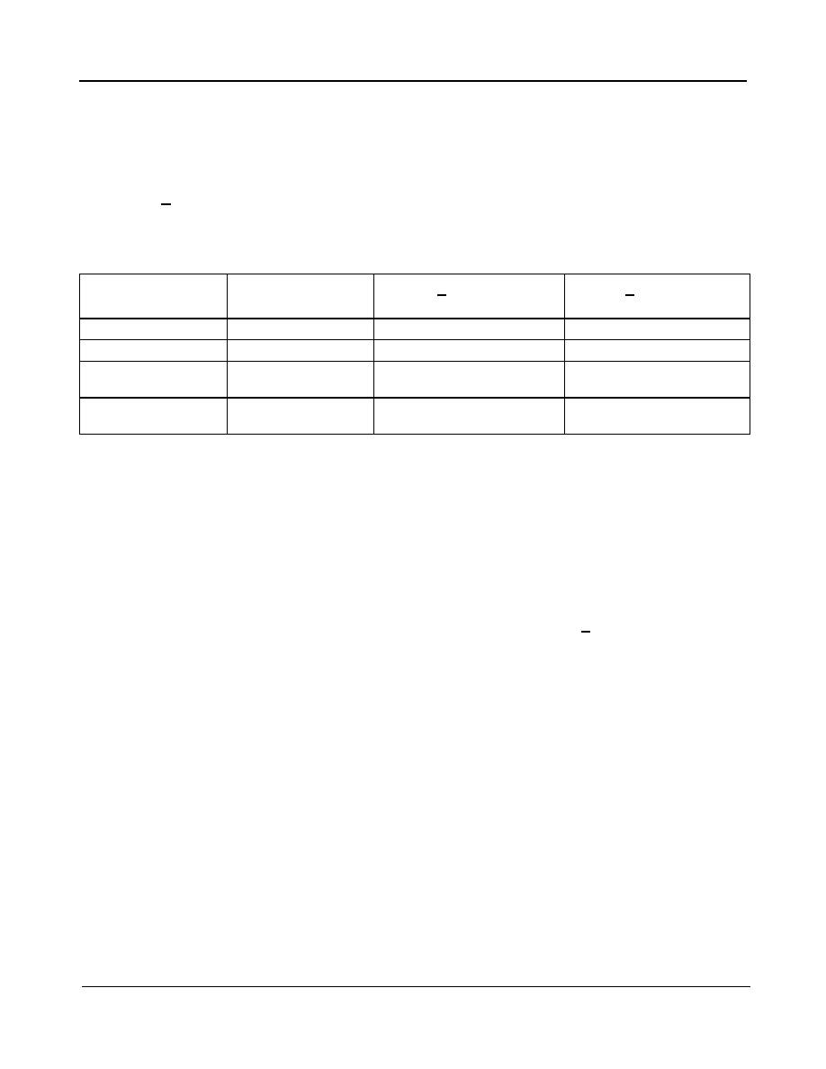
ZL50015
Data Sheet
48
Zarlink Semiconductor Inc.
19.0 PCM A-law/
µ
-law Translation
The ZL50015 provides per-channel code translation to be used to adapt pulse code modulation (PCM) voice or
data traffic between networks which use different encoding laws. Code translation is valid in both Connection Mode
and Message Mode.
In order to use this feature the Connection Memory High (CM_H) entry for the output channel must be
programmed. V/D (bit 4) defines if the traffic in the channel is voice or data. Setting ICL1 - 0 (bits 3 - 2) programs the
input coding law and OCL1 - 0 (bits 1- 0) programs the output coding law as shown in Table 13.
The different code options are:
For voice coding options, the ITU-T G.711 A-law and ITU-T G.711
µ-law are the standard rules for encoding. A-law
without Alternate Bit Inversion (ABI) is an alternative code that does not invert the even bits (6, 4, 2, 0).
µ-law
without Magnitude Inversion (MI) is an alternative code that does not perform inversion of magnitude bits (6, 5, 4, 3,
2, 1, 0).
When transferring data code, the option "no code" does not invert the bits. The Alternate Bit Inversion (ABI) option
inverts the even bits (6, 4, 2, 0) while the Inverted Alternate Bit Inversion (ABI) inverts the odd bits (7, 5, 3, 1). When
the "All bits inverted" option is selected, all of the bits (7, 6, 5, 4, 3, 2, 1, 0) are inverted.
The input channel and output channel encoding law are configured independently. If the output channel coding is
set to be different from the input channel, the ZL50015 performs translation between the two standards. If the input
and output encoding laws are set to the same standard, no translation occurs. As the V/D (bit 4) of the Connection
Memory High (CM_H) must be set on a per-channel basis, it is not possible to translate between voice and data
encoding laws.
Input Coding
(ICL1- 0)
Output Coding
(OCL1 - 0)
Voice Coding
(V/D bit = 0)
Data Coding
(V/D bit = 1)
00
00
ITU-T G.711 A-law
No code
01
01
ITU-T G.711
µ-law
Alternate Bit Inversion (ABI)
10
10
A-law without Alternate Bit
Inversion (ABI)
Inverted Alternate Bit
Inversion (ABI)
11
11
µ-law without Magnitude
Inversion (MI)
All bits inverted
Table 13 - Input and Output Voice and Data Coding
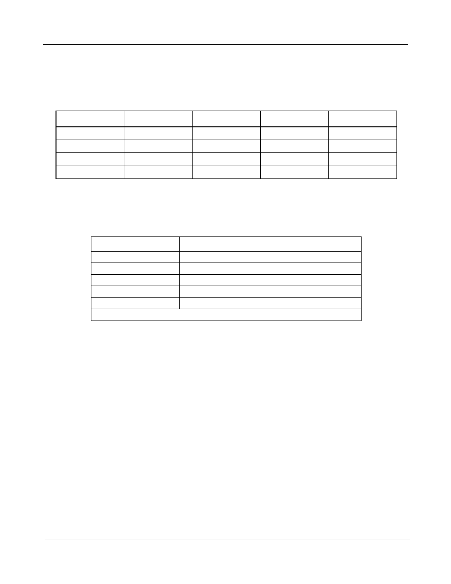
ZL50015
Data Sheet
49
Zarlink Semiconductor Inc.
20.0 Quadrant Frame Programming
By programming the Stream Input Quadrant Frame Registers (SIQFR0 - 15), users can divide one frame of input
data into four quadrant frames and can force the LSB or MSB of every input channel in these quadrants to one or
zero for robbed-bit signaling. The four quadrant frames are defined as follows:
When the quadrant frame control bits, STIN[n]Q3C2 - 0 (bit 11 - 9), STIN[n]Q2C2 - 0 (bit 8 - 6), STIN[n]Q1C2 - 0 (bit
5 - 3) or STIN[n]Q1C2 - 0 (bit 2 - 0), are set, the LSB or MSB of every input channel in the quadrant is forced to "1"
or "0" as shown by the following table:
Note that Quadrant Frame Programming and BER reception cannot be used simultaneously on the same input
stream.
21.0 JTAG Port
The JTAG test port is implemented to meet the mandatory requirements of the IEEE-1149.1 (JTAG) standard. The
operation of the boundary-scan circuitry is controlled by an external Test Access Port (TAP) Controller.
21.1 Test Access Port (TAP)
The Test Access Port (TAP) accesses the ZL50015 test functions. It consists of three input pins and one output pin
as follows:
∑ Test Clock Input (TCK) - TCK provides the clock for the test logic. TCK does not interfere with any on-chip
clock and thus remains independent in the functional mode. TCK permits shifting of test data into or out of
the Boundary-Scan register cells concurrently with the operation of the device and without interfering with
the on-chip logic.
∑ Test Mode Selection Inputs (TMS) - The TAP Controller uses the logic signals received at the TMS input to
control test operations. The TMS signals are sampled at the rising edge of the TCK pulse. This pin is
internally pulled to high when it is not driven from an external source.
Data Rate
Quadrant 0
Quadrant 1
Quadrant 2
Quadrant 3
2.048 Mbps
Channel 0 - 7
Channel 8 - 15
Channel 16 - 23
Channel 24 - 31
4.096 Mbps
Channel 0 - 15
Channel 16 - 31
Channel 32 - 47
Channel 48 - 63
8.192 Mbps
Channel 0 - 31
Channel 32 - 63
Channel 64 - 95
Channel 96 - 127
16.384 Mbps
Channel 0 - 63
Channel 64 - 127
Channel 128 - 191
Channel 192 - 255
Table 14 - Definition of the Four Quadrant Frames
STIN[n]Q[y]C[2:0]
Action
0xx
Normal Operation
100
Replaces LSB of every channel in Quadrant y with `0'
101
Replaces LSB of every channel in Quadrant y with `1'
110
Replaces MSB of every channel in Quadrant y with `0'
111
Replaces MSB of every channel in Quadrant y with `1'
Note: y = 0, 1, 2, 3
Table 15 - Quadrant Frame Bit Replacement

ZL50015
Data Sheet
50
Zarlink Semiconductor Inc.
∑ Test Data Input (TDi) - Serial input data applied to this port is fed either into the instruction register or into a
test data register, depending on the sequence previously applied to the TMS input. The registers are
described in a subsequent section. The received input data is sampled at the rising edge of the TCK pulse.
This pin is internally pulled to high when it is not driven from an external source.
∑ Test Data Output (TDo) - Depending on the sequence previously applied to the TMS input, the contents of
either the instruction register or test data register are serially shifted out towards TDo. The data from TDo is
clocked on the falling edge of the TCK pulses. When no data is shifted through the boundary scan cells, the
TDo driver is set to a high impedance state.
∑ Test Reset (TRST) - Resets the JTAG scan structure. This pin is internally pulled to high when it is not
driven from an external source.
21.2 Instruction Register
The ZL50015 uses the public instructions defined in the IEEE-1149.1 standard. The JTAG interface contains a
four-bit instruction register. Instructions are serially loaded into the instruction register from the TDi when the TAP
Controller is in its shifted-OR state. These instructions are subsequently decoded to achieve two basic functions: to
select the test data register that may operate while the instruction is current and to define the serial test data
register path that is used to shift data between TDi and TDo during data register scanning.
21.3 Test Data Registers
As specified in the IEEE-1149.1 standard, the ZL50015 JTAG interface contains three test data registers:
∑ The Boundary-Scan Register - The Boundary-Scan register consists of a series of boundary-scan cells
arranged to form a scan path around the boundary of the ZL50015 core logic.
∑ The Bypass Register - The Bypass register is a single stage shift register that provides a one-bit path from
TDi to TDo.
∑ The Device Identification Register - The JTAG device ID for the ZL50015 is 0C36F14B
H
21.4 BSDL
A Boundary Scan Description Language (BSDL) file is available from Zarlink Semiconductor to aid in the use of the
IEEE-1149.1 test interface.
Version
<31:28>
0000
Part Number
<27:12>
1100 0011 0110 1111
Manufacturer ID
<11:1>
0001 0100 101
LSB
<0>
1

ZL50015
Data Sheet
51
Zarlink Semiconductor Inc.
22.0 Register Address Mapping
Address
A13 - A0
CPU
Access
Register
Name
Abbreviation
Reset By
0000
H
R/W
Control Register
CR
Switch/Hardware
0001
H
R/W
Internal Mode Selection Register
IMS
Switch/Hardware
0002
H
R/W
Software Reset Register
SRR
Hardware Only
0003
H
R/W
Output Clock and Frame Pulse Control Register
OCFCR
DPLL/Hardware
0004
H
R/W
Output Clock and Frame Pulse Selection
Register
OCFSR
DPLL/Hardware
0005
H
R/W
FPo_OFF0 Register
FPOFF0
DPLL/Hardware
0006
H
R/W
FPo_OFF1 Register
FPOFF1
DPLL/Hardware
0007
H
R/W
FPo_OFF2 Register
FPOFF2
DPLL/Hardware
0010
H
R Only
Internal Flag Register
IFR
Switch/Hardware
0011
H
R Only
BER Error Flag Register 0
BERFR0
Switch/Hardware
0013
H
R Only
BER Receiver Lock Register 0
BERLR0
Switch/Hardware
0040
H
R/W
DPLL Control Register
DPLLCR
DPLL/Hardware
0041
H
R/W
Reference Frequency Register
RFR
DPLL/Hardware
0042
H
R/W
Centre Frequency Register - Lower 16 Bits
CFRL
DPLL/Hardware
0043
H
R/W
Centre Frequency Register - Upper 10 Bits
CFRU
DPLL/Hardware
0045
H
R Only
Frequency Offset Register
FOR
DPLL/Hardware
0047
H
R/W
Lock Detector Threshold Register
LDTR
DPLL/Hardware
0048
H
R/W
Lock Detector Interval Register
LDIR
DPLL/Hardware
0049
H
R/W
Slew Rate Limit Register
SRLR
DPLL/Hardware
004B
H
R/W
Reference Change Control Register
RCCR
DPLL/Hardware
004C
H
R Only
Reference Change Status Register
RCSR
DPLL/Hardware
0066
H
R Only
Interrupt Register
IR
DPLL/Hardware
0067
H
R/W
Interrupt Mask Register
IMR
DPLL/Hardware
0068
H
R/W
Interrupt Clear Register
ICR
DPLL/Hardware
0069
H
R Only
Reference Failure Status Register
RSR
DPLL/Hardware
006A
H
R/W
Reference Mask Register
RMR
DPLL/Hardware
006B
H
R Only
Reference Frequency Status Register
RFSR
DPLL/Hardware
006C
H
R/W
Output Jitter Control Register
OJCR
DPLL/Hardware
0100
H
-
010F
H
R/W
Stream Input Control Registers 0 - 15
SICR0 - 15
Switch/Hardware
Table 16 - Address Map for Registers (A13 = 0)
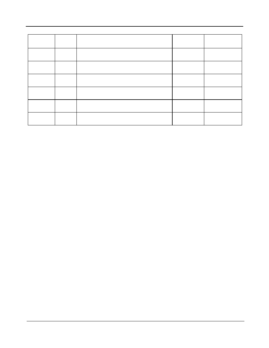
ZL50015
Data Sheet
52
Zarlink Semiconductor Inc.
0120
H
-
012F
H
R/W
Stream Input Quadrant Frame Registers 0 - 15
SIQFR0 - 15
Switch/Hardware
0200
H
-
020F
H
R/W
Stream Output Control Registers 0 - 15
SOCR0 - 15
Switch/Hardware
0300
H
-
030F
H
R/W
BER Receiver Start Registers 0 - 15
BRSR0 - 15
Switch/Hardware
0320
H
-
032F
H
R/W
BER Receiver Length Registers 0 - 15
BRLR0 - 15
Switch/Hardware
0340
H
-
034F
H
R/W
BER Receiver Control Registers 0 - 15
BRCR0 - 15
Switch/Hardware
0360
H
-
036F
H
R Only
BER Receiver Error Registers 0 - 15
BRER0 - 15
Switch/Hardware
Address
A13 - A0
CPU
Access
Register
Name
Abbreviation
Reset By
Table 16 - Address Map for Registers (A13 = 0) (continued)

ZL50015
Data Sheet
53
Zarlink Semiconductor Inc.
23.0 Detailed Register Description
Bit
Name
Description
15 - 14
Unused
Reserved. In normal functional mode, these bits MUST be set to zero.
13
SLV_
DPLLEN
DPLL Enable in Slave Mode (ignored in Master Mode)
When this bit is low, DPLL is disabled in Slave mode.
When this bit is high and OSC_EN = 1, the DPLL is enabled in Slave mode.
When SLV_DPLLEN is set in Slave mode, CKo[3:0] and FPo[3:0] are generated from
CKi and FPi. CKo[5:4] and FPo[5] are locked to the selected input reference (one of
REF[3:0]). In this mode of operation, the DPLL retains its functionality, including the
generation of the REF_FAIL[3:0] output signals. See Table 7, "ZL50015 Operating
Modes" on page 37 for more details.
12 - 11
OPM1 - 0
Operation Mode.
These bits are used to set the device in Master/Slave operation. Refer to Table 7,
"ZL50015 Operating Modes" on page 37 for more details.
10
CKi_LP
CKi and FPi Loopback (Ignored in Slave mode)
When this bit is low, CKi and FPi are used as input pins.
When this bit is high, CKi and FPi are internally looped back from CKo2 (16.384 MHz)
and FPo2 respectively, and CKi pin and FPi pin should be tied low or high externally;
CKIN1 - 0 (bits 6 - 5) of this register should be programmed to be 00. See Table 7,
"ZL50015 Operating Modes" on page 37 for more details.
9
FPINPOS
Input Frame Pulse (FPi) Position
When this bit is low, FPi straddles frame boundary (as defined by ST-BUS).
When this bit is high, FPi starts from frame boundary (as defined by GCI-Bus)
8
CKINP
Clock Input (CKi) Polarity
When this bit is low, the CKi falling edge aligns with the frame boundary.
When this bit is high, the CKi rising edge aligns with the frame boundary.
7
FPINP
Frame Pulse Input (FPi) Polarity
When this bit is low, the input frame pulse FPi has the negative frame pulse format.
When this bit is high, the input frame pulse FPi has the positive frame pulse format.
Table 17 - Control Register (CR) Bits
External Read/Write Address: 0000
H
Reset Value: 0000
H
15
14
13
12
11
10
9
8
7
6
5
4
3
2
1
0
0
0
SLV_
DPLLEN
OPM
1
OPM
0
CKi_
LP
FPIN
POS
CKINP
FPINP
CKIN
1
CKIN
0
VAR
EN
MBPE
OSB
MS1
MS0
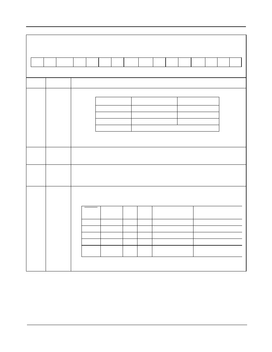
ZL50015
Data Sheet
54
Zarlink Semiconductor Inc.
6 - 5
CKIN1 - 0
Input Clock (CKi) and Frame Pulse (FPi) Selection
The MODE_4M0 and MODE_4M1 pins, as described in "Pin Description" on page 13,
should also be set to define the input clock mode.
4
VAREN
Variable Delay Mode Enable
When this bit is low, the variable delay mode is disabled on a device-wide basis.
When this bit is high, the variable delay mode is enabled on a device-wide basis.
3
MBPE
Memory Block Programming Enable
When this bit is high, the connection memory block programming mode is enabled to
program the connection memory. When it is low, the memory block programming mode is
disabled.
2
OSB
Output Stand By Bit:
This bit enables the STio0 - 15 and the STOHZ0 -7 serial outputs. The following table
describes the HiZ control of the serial data outputs:
Note: Unused output streams are tristated (STio = HiZ, STOHZ = Driven High). Refer to
SOCR0 - 15 (bit2 - 0).
Bit
Name
Description
Table 17 - Control Register (CR) Bits (continued)
External Read/Write Address: 0000
H
Reset Value: 0000
H
15
14
13
12
11
10
9
8
7
6
5
4
3
2
1
0
0
0
SLV_
DPLLEN
OPM
1
OPM
0
CKi_
LP
FPIN
POS
CKINP
FPINP
CKIN
1
CKIN
0
VAR
EN
MBPE
OSB
MS1
MS0
CKIN1 - 0
FPi Active Period
CKi
00
61 ns
16.384 MHz
01
122 ns
8.192 MHz
10
244 ns
4.096 MHz
11
Reserved
RESET
Pin
SRSTSW
(in SRR)
ODE
Pin
OSB
Bit
STio0 - 15
STOHZ0 - 7
0
X
X
X
HiZ
Driven High
1
1
X
X
HiZ
Driven High
1
0
0
X
HiZ
Driven High
1
0
1
0
HiZ
Driven High
1
0
1
1
Active
(Controlled by CM)
Active
(Controlled by CM)
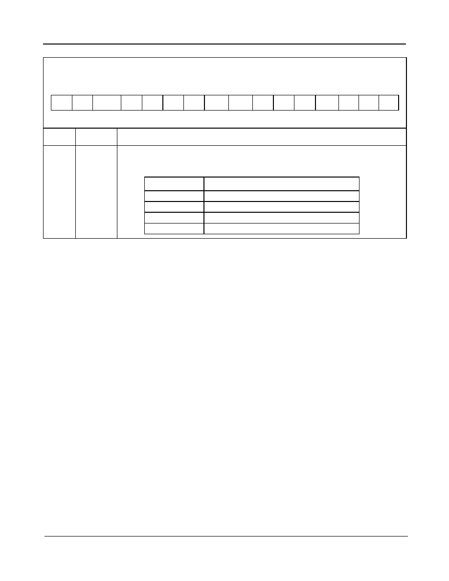
ZL50015
Data Sheet
55
Zarlink Semiconductor Inc.
1 - 0
MS1 - 0
Memory Select Bits
These two bits are used to select connection memory low, connection high or data mem-
ory for access by CPU:
Bit
Name
Description
Table 17 - Control Register (CR) Bits (continued)
External Read/Write Address: 0000
H
Reset Value: 0000
H
15
14
13
12
11
10
9
8
7
6
5
4
3
2
1
0
0
0
SLV_
DPLLEN
OPM
1
OPM
0
CKi_
LP
FPIN
POS
CKINP
FPINP
CKIN
1
CKIN
0
VAR
EN
MBPE
OSB
MS1
MS0
MS1 - 0
Memory Selection
00
Connection Memory Low Read/Write
01
Connection Memory High Read/Write
10
Data Memory Read
11
Reserved
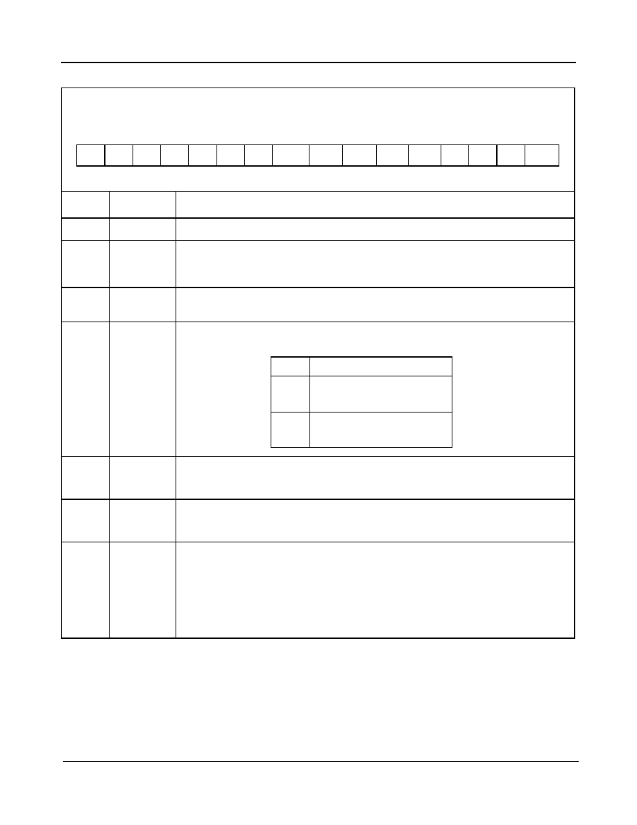
ZL50015
Data Sheet
56
Zarlink Semiconductor Inc.
Bit
Name
Description
15 - 9
Unused
Reserved. In normal functional mode, these bits MUST be set to zero.
8
STIO_PD_
EN
STio Pull-down Enable
When this bit is low, the pull-down resistors on all STio pads will be disabled.
When this bit is high, the pull-down resistors on all STio pads will be enabled.
7
Unused
Reserved. In normal functional mode, these bits MUST be set to zero.
Used in this bi-directional mode.
6
BDL
Bi-directional Control for Streams 0-15
5
RBEREN
PRBS Receiver Enable
When this bit is low, all the BER receivers are disabled. To enable any BER receivers,
this bit MUST be high.
4
TBEREN
PRBS Transmitter Enable
When this bit is low, all the BER transmitters are disabled. To enable any BER
transmitters, this bit MUST be high.
3 - 1
BPD2 - 0
Block Programming Data
These bits refer to the value to be loaded into the connection memory, whenever the
memory block programming feature is activated. After the MBPE bit in the Control
Register is set to high and the MBPS bit in this register is set to high, the contents of
the bits BPD2 - 0 are loaded into bits 2 - 0 of the Connection Memory Low. Bits 15 - 3
of the Connection Memory Low and bits 15 - 0 of Connection Memory High are
zeroed.
Table 18 - Internal Mode Selection Register (IMS) Bits
External Read/Write Address: 0001
H
Reset Value: 0000
H
15
14
13
12
11
10
9
8
7
6
5
4
3
2
1
0
0
0
0
0
0
0
0
STIO_
PD_EN
0
BDL
RBER
EN
TBER
EN
BPD
2
BPD
1
BPD
0
MBPS
BDL
STio0 - 15 Operation
0
normal operation:
STi0-15 are inputs
STio0-15 are outputs
1
bi-directional operation:
STi0-15 tied low internally
STio0-15 are bi-directional
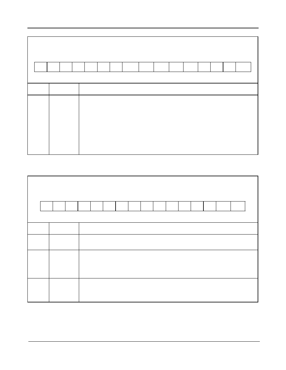
ZL50015
Data Sheet
57
Zarlink Semiconductor Inc.
0
MBPS
Memory Block Programming Start:
A zero to one transition of this bit starts the memory block programming function. The
MBPS and BPD2 - 0 bits in this register must be defined in the same write operation.
Once the MBPE bit in the Control Register is set to high, the device requires two
frames to complete the block programming. After the programming function has fin-
ished, the MBPS bit returns to low, indicating the operation is completed. When MBPS
is high, MBPS or MBPE can be set to low to abort the programming operation.
Whenever the microprocessor writes a one to the MBPS bit, the block programming
function is started. As long as this bit is high, the user must maintain the same logical
value to the other bits in this register to avoid any change in the device setting.
Bit
Name
Description
15 - 2
Unused
Reserved
In normal functional mode, these bits MUST be set to zero.
1
SRSTSW
Software Reset Bit for Switch
When this bit is low, data switching blocks are in normal operation. When this bit is
high, data switching blocks are in software reset state. Refer to Table 16, "Address
Map for Registers (A13 = 0)" on page 51 for details regarding which registers are
affected.
0
SRSTDPLL
Software Reset Bit for DPLL
When this bit is low, the DPLL block is in normal operation. When this bit is high, the
DPLL block is in software reset state. Refer to Table 16, "Address Map for Registers
(A13 = 0)" on page 51 for details regarding which registers are affected.
Table 19 - Software Reset Register (SRR) Bits
Bit
Name
Description
Table 18 - Internal Mode Selection Register (IMS) Bits (continued)
External Read/Write Address: 0001
H
Reset Value: 0000
H
15
14
13
12
11
10
9
8
7
6
5
4
3
2
1
0
0
0
0
0
0
0
0
STIO_
PD_EN
0
BDL
RBER
EN
TBER
EN
BPD
2
BPD
1
BPD
0
MBPS
External Read/Write Address: 0002
H
Reset Value: 0000
H
15
14
13
12
11
10
9
8
7
6
5
4
3
2
1
0
0
0
0
0
0
0
0
0
0
0
0
0
0
0
SRST
SW
SRST
DPLL
ZL50015
Data Sheet
58
Zarlink Semiconductor Inc.
Bit
Name
Description
15 - 9
Unused
Reserved
In normal functional mode, these bits MUST be set to zero.
8
FPOF2EN
FPo_OFF2/FPo5 Enable
When this bit is high, output frame pulse FPo_OFF2/FPo5 is enabled.
When this bit is low, output frame pulse FPo_OFF2/FPo5 is in high impedance state.
7
FPOF1EN
FPo_OFF1 Enable
When this bit is high, output frame pulse FPo_OFF1 is enabled.
When this bit is low, output frame pulse FPo_OFF1 is in high impedance state.
6
FPOF0EN
FPo_OFF0 Enable
When this bit is high, output frame pulse FPo_OFF0 is enabled.
When this bit is low, output frame pulse FPo_OFF0 is in high impedance state.
5
CKO5EN
CKo5 Enable
When this bit is high, output clock CKo5 is enabled.
When this bit is low, output clock CKo5 is in high impedance state.
CKo5 is available in Master mode or in Slave mode with SLV_DPLLEN set.
4
CKO4EN
CKo4 Enable
When this bit is high, output clock CKo4 is enabled.
When this bit is low, output clock CKo4 is in high impedance state.
CKo4 is available in Master mode or in Slave mode with SLV_DPLLEN set.
3
CKOFPO3
EN
CKo3 and FPo3 Enable
When this bit is high, output clock CKo3 and output frame pulse FPo3 are enabled.
When this bit is low, CKo3 and FPo3 are in high impedance state.
2
CKOFPO2
EN
CKo2 and FPo2 Enable
When this bit is high, output clock CKo2 and output frame pulse FPo2 are enabled.
When this bit is low, CKo2 and FPo2 are in high impedance state.
1
CKOFPO1
EN
CKo1 and FPo1 Enable
When this bit is high, output clock CKo1 and output frame pulse FPo1 are enabled.
When this bit is low, CKo1 and FPo1 are in high impedance state.
0
CKOFPO0
EN
CKo0 and FPo0 Enable
When this bit is high, output clock CKo0 and output frame pulse FPo0 are enabled.
When this bit is low, CKo0 and FPo0 are in high impedance state.
Table 20 - Output Clock and Frame Pulse Control Register (OCFCR) Bits
External Read/Write Address: 0003
H
Reset Value: 0000
H
15
14
13
12
11
10
9
8
7
6
5
4
3
2
1
0
0
0
0
0
0
0
0
FPOF2
EN
FPOF1
EN
FPOF0
EN
CKO5
EN
CKO4
EN
CKO
FPO3
EN
CKO
FPO2
EN
CKO
FPO1
EN
CKO
FPO0
EN
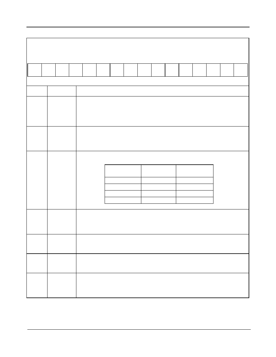
ZL50015
Data Sheet
59
Zarlink Semiconductor Inc.
Bit
Name
Description
15
CKO4P
Output Clock (CKo4) Polarity Selection
When this bit is low, the output clock CKo4 falling edge aligns with the frame
boundary. When this bit is high, the output clock CKo4 rising edge aligns with the
frame boundary.
CKo4 is available in Master mode or in Slave mode with SLV_DPLLEN set.
14
CKO4SEL
Output Clock (CKo4) Frequency Selection
When this bit is low, the output clock CKo4 is 2.048 MHz.
When this bit is high, the output clock CKo4 is 1.544 MHz.
CKo4 is available in Master mode or in Slave mode with SLV_DPLLEN set.
13 - 12
CKOFPO3
SEL1 - 0
Output Clock (CKo3) Frequency and Output Frame Pulse (FPo3) Pulse Cycle
Selection
11
CKO3P
Output Clock (CKo3) Polarity Selection
When this bit is low, the output clock CKo3 falling edge aligns with the frame
boundary. When this bit is high, the output clock CKo3 rising edge aligns with the
frame boundary.
10
FPO3P
Output Frame Pulse (FPo3) Polarity Selection
When this bit is low, the output frame pulse FPo3 has the negative frame pulse format.
When this bit is high, the output frame pulse FPo3 has the positive frame pulse format.
9
FPO3POS
Output Frame Pulse (FPo3) Position
When this bit is low, FPo3 straddles frame boundary (as defined by ST-BUS).
When this bit is high, FPo3 starts from frame boundary (as defined by GCI-Bus).
8
CKO2P
Output Clock (CKo2) Polarity Selection
When this bit is low, the output clock CKo2 falling edge aligns with the frame
boundary. When this bit is high, the output clock CKo2 rising edge aligns with the
frame boundary.
Table 21 - Output Clock and Frame Pulse Selection Register (OCFSR) Bits
External Read/Write Address: 0004
H
Reset Value: 0000
H
15
14
13
12
11
10
9
8
7
6
5
4
3
2
1
0
CKO4
P
CKO4
SEL
CKO
FPO3
SEL1
CKO
FPO3
SEL0
CKO3
P
FPO3
P
FPO3
POS
CKO2
P
FPO2
P
FPO2
POS
CKO1
P
FPO1
P
FPO1
POS
CKO0
P
FPO0
P
FPO0
POS
CKOFPO3
SEL1 - 0
FPo3
CKo3
00
244 ns
4.096 MHz
01
122 ns
8.192 MHz
10
61 ns
16.384 MHz
11
30 ns
32.768 MHz

ZL50015
Data Sheet
60
Zarlink Semiconductor Inc.
7
FPO2P
Output Frame Pulse (FPo2) Polarity Selection
When this bit is low, the output frame pulse FPo2 has the negative frame pulse format.
When this bit is high, the output frame pulse FPo2 has the positive frame pulse format.
6
FPO2POS
Output Frame Pulse (FPo2) Position
When this bit is low, FPo2 straddles frame boundary (as defined by ST-BUS).
When this bit is high, FPo2 starts from frame boundary (as defined by GCI-Bus).
5
CKO1P
Output Clock (CKo1) Polarity Selection
When this bit is low, the output clock CKo1 falling edge aligns with the frame
boundary. When this bit is high, the output clock CKo1 rising edge aligns with the
frame boundary.
4
FPO1P
Output Frame Pulse (FPo1) Polarity Selection
When this bit is low, the output frame pulse FPo1 has the negative frame pulse format.
When this bit is high, the output frame pulse FPo1 has the positive frame pulse format.
3
FPO1POS
Output Frame Pulse (FPo1) Position
When this bit is low, FPo1 straddles frame boundary (as defined by ST-BUS).
When this bit is high, FPo1 starts from frame boundary (as defined by GCI-Bus).
2
CKO0P
Output Clock (CKo0) Polarity Selection
When this bit is low, the output clock CKo0 falling edge aligns with the frame
boundary. When this bit is high, the output clock CKo0 rising edge aligns with the
frame boundary.
1
FPO0P
Output Frame Pulse (FPo0) Polarity Selection
When this bit is low, the output frame pulse FPo0 has the negative frame pulse format.
When this bit is high, the output frame pulse FPo0 has the positive frame pulse format.
0
FPO0POS
Output Frame Pulse (FPo0) Position
When this bit is low, FPo0 straddles frame boundary (as defined by ST-BUS).
When this bit is high, FPo0 starts from frame boundary (as defined by GCI-Bus).
Note: In Divided Slave modes, CKo3 - 1 cannot exceed frequency of CKi.
Note: CKo[5:4] are available in Master mode or in Slave mode with SLV_DPLLEN set.
Bit
Name
Description
Table 21 - Output Clock and Frame Pulse Selection Register (OCFSR) Bits (continued)
External Read/Write Address: 0004
H
Reset Value: 0000
H
15
14
13
12
11
10
9
8
7
6
5
4
3
2
1
0
CKO4
P
CKO4
SEL
CKO
FPO3
SEL1
CKO
FPO3
SEL0
CKO3
P
FPO3
P
FPO3
POS
CKO2
P
FPO2
P
FPO2
POS
CKO1
P
FPO1
P
FPO1
POS
CKO0
P
FPO0
P
FPO0
POS
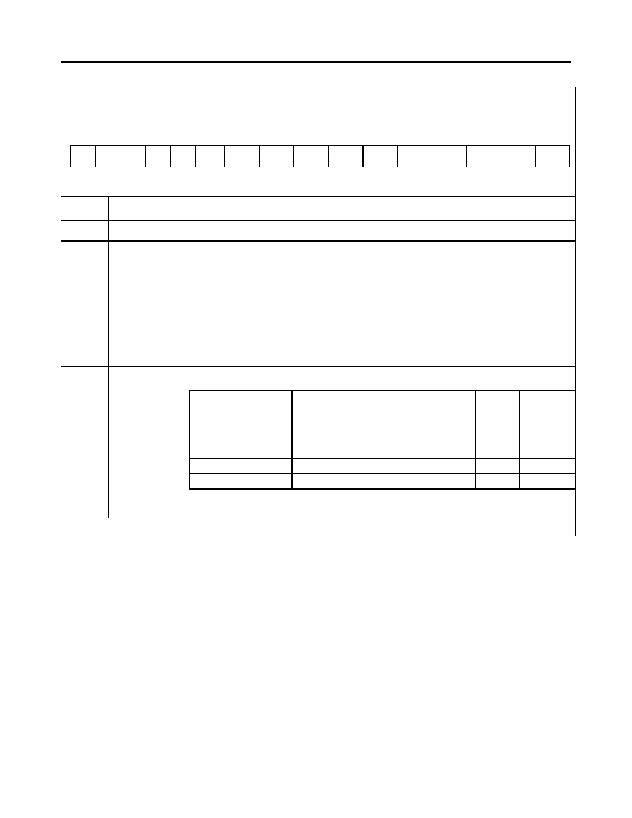
ZL50015
Data Sheet
61
Zarlink Semiconductor Inc.
Bit
Name
Description
15 - 11
Unused
Reserved. In normal functional mode, these bits MUST be set to zero.
10
FP19EN
19.44 MHz Frame Pulse Output Enable. (For FPo_OFF2 only)
This bit is a reserved bit for FPo_OFF0 and FPo_OFF1, and MUST be set to
zero.
When this bit is high, FPo_OFF2 is negative frame pulse output corresponding to
19.44 MHz without channel offset.
When this bit is low, FPo_OFF2 is output frame pulse with channel offset.
9 - 2
FOF[n]OFF7 - 0
FPo_OFF[n] Channel Offset
The binary value of these bits refers to the channel offset from original frame bound-
ary. Permitted channel offset values depend on bits 1-0 of this register.
1 - 0
FOF[n]C1 - 0
FPo_OFF[n] Control bits
Note: [n] denotes output offset frame pulse from 0 to 2.
Table 22 - FPo_OFF[n] Register (FPo_OFF[n]) Bits
External Read/Write Address: 0005
H
- 0007
H
Reset Value: 0000
H
15
14
13
12
11
10
9
8
7
6
5
4
3
2
1
0
0
0
0
0
0
FP19
EN
FOF[n]
OFF7
FOF[n]
OFF6
FOF[n]
OFF5
FOF[n]
OFF4
FOF[n]
OFF3
FOF[n]
OFF2
FOF[n]
OFF1
FOF[n]
OFF0
FOF[n]
C1
FOF[n]
C0
FOF[n]C
1-0
Data Rate
(Mbps)
FPo_OFF[n]
Pulse Cycle Width
FOF[n]OFF7 - 0
Permitted
Channel Offset
Polarity
Control
Position
Control
00
2.048
one 4.096 MHz clock
0 - 31
FPO0P
FPO0POS
01
4.096
one 8.192 MHz clock
0 - 63
FPO1P
FPO1POS
10
8.192
one 16.384 MHz clock
0 - 127
FPO2P
FPO2POS
11
16.384
one 16.384 MHz clock
0 - 255
FPO2P
FPO2POS
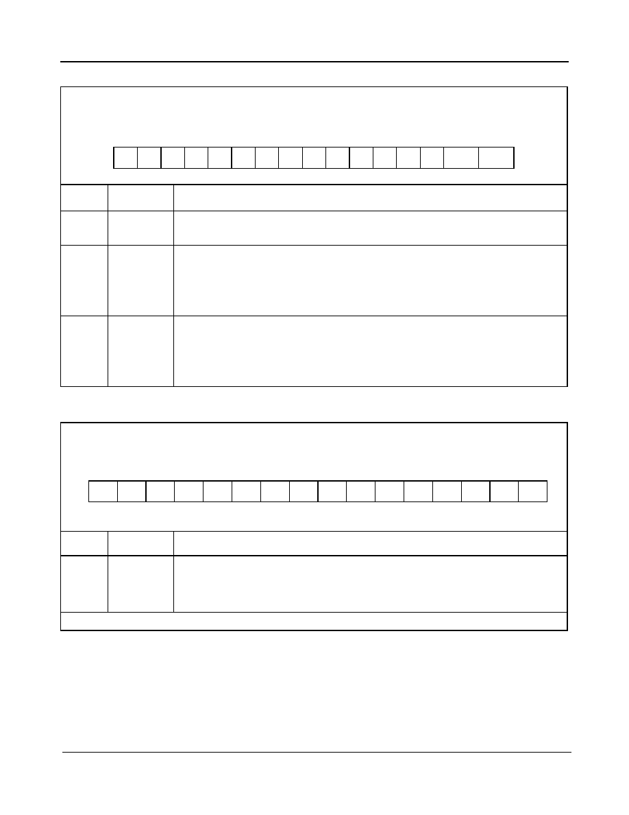
ZL50015
Data Sheet
62
Zarlink Semiconductor Inc.
Bit
Name
Description
15 - 2
Unused
Reserved
In normal functional mode, these bits are zero.
1
OUTERR
Output Error (Read Only)
This bit is set high when the total number of output channels is programmed to be
more than the maximum capacity of 1024, in which case the output channels beyond
the maximum capacity should be disabled.
This bit will be cleared automatically after programming is corrected.
0
INERR
Input Error (Read Only)
This bit is set high when the total number of input channels is programmed to be more
than the maximum capacity of 1024, in which case the input channels beyond the
maximum capacity should be disabled.This bit will be cleared automatically after pro-
gramming is corrected.
Table 23 - Internal Flag Register (IFR) Bits - Read Only
Bit
Name
Description
15 - 0
BERF[n]
BER Error Flag[n]:
If BERF[n] is high, it indicates that BER Receiver Error Register [n] (BRER[n]) is not
zero.
If BERF[n] is low, it indicates that BER Receiver Error Register [n] (BRER[n]) is zero.
Note: [n] denotes input stream from 0 -15.
Table 24 - BER Error Flag Register 0 (BERFR0) Bits - Read Only
External Read Address: 0010
H
Reset Value: 0000
H
15
14
13
12
11
10
9
8
7
6
5
4
3
2
1
0
0
0
0
0
0
0
0
0
0
0
0
0
0
0
OUT
ERR
IN
ERR
External Read Address: 00011
H
Reset Value: 0000
H
15
14
13
12
11
10
9
8
7
6
5
4
3
2
1
0
BER
F15
BER
F14
BER
F13
BER
F12
BER
F11
BER
F10
BER
F9
BER
F8
BER
F7
BER
F6
BER
F5
BER
F4
BER
F3
BER
F2
BER
F1
BER
F0
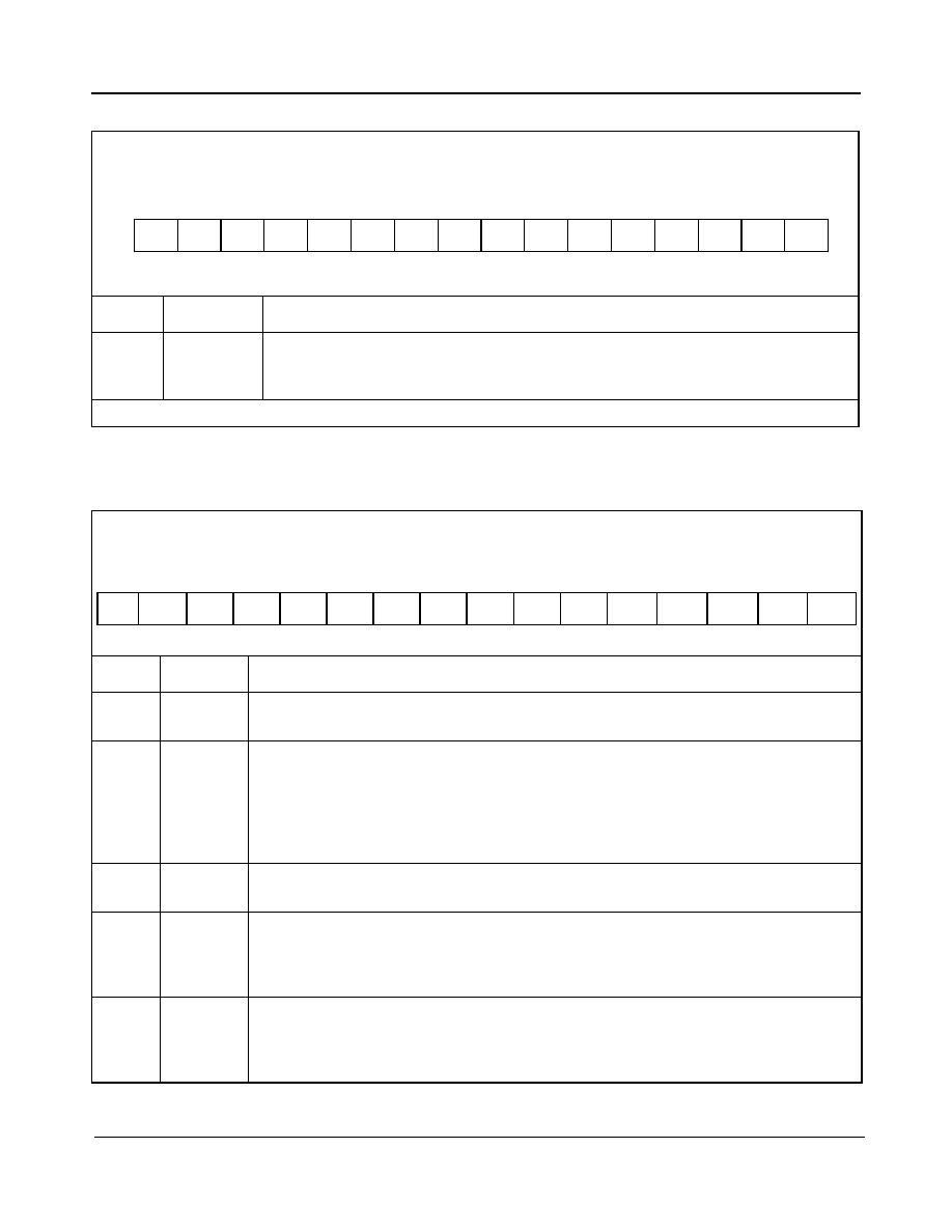
ZL50015
Data Sheet
63
Zarlink Semiconductor Inc.
Bit
Name
Description
15 - 0
BERL[n]
BER Receiver Lock[n]
If BERL[n] is high, it indicates that BER Receiver of STi[n] is locked.
If BERL[n] is low, it indicates that BER Receiver of STi[n] is not locked.
Note: [n] denotes input stream from 0 - 15.
Table 25 - BER Receiver Lock Register 0 (BERLR0) Bits - Read Only
Bit
Name
Description
15-6
Unused
Reserved
In normal functional mode, these bits MUST be set to zero.
5
ST4_LIM
Stratum 4E Limits Select Bit
When this bit is high, the stratum 4E limits are used for reference monitoring (i.e.,
+/-64.713 ppm and +/-82.487 ppm over 10 seconds). When this bit is low, more relaxed
Relaxed Stratum 4E limits are used for reference monitoring (e.g., +/-240 ppm and
+/-250 ppm over 10 seconds). This is used in applications where a low quality clock
(+/-100 ppm) is used as a reference.
4-2
Unused
Reserved
In normal functional mode, these bits MUST be set to zero.
1
RFRE
Reference Frequency Register Enable
When this bit is low, the reference frequency value used in the DPLL comes from
appropriate reference frequency detector. When this bit is high, the reference frequency
value comes from Reference Frequency Register (RFR).
0
DPLL_
IRM
DPLL Internal Reset Mode
When this bit is low, the DPLL module is in the operational state. When this bit is high,
the DPLL module is in the power saving mode. Registers are not reset and are still
accessible in the power saving mode.
Table 26 - DPLL Control Register (DPLLCR) Bits
External Read Address: 00013
H
Reset Value: 0000
H
15
14
13
12
11
10
9
8
7
6
5
4
3
2
1
0
BER
L15
BER
L14
BER
L13
BER
L12
BER
L11
BER
L10
BER
L9
BER
L8
BER
L7
BER
L6
BER
L5
BER
L4
BER
L3
BER
L2
BER
L1
BER
L0
External Read/Write Address: 0040
H
Reset Value: 0000
H
15
14
13
12
11
10
9
8
7
6
5
4
3
2
1
0
0
0
0
0
0
0
0
0
0
0
ST4_
LIM
0
0
0
RFRE
DPLL
_IRM
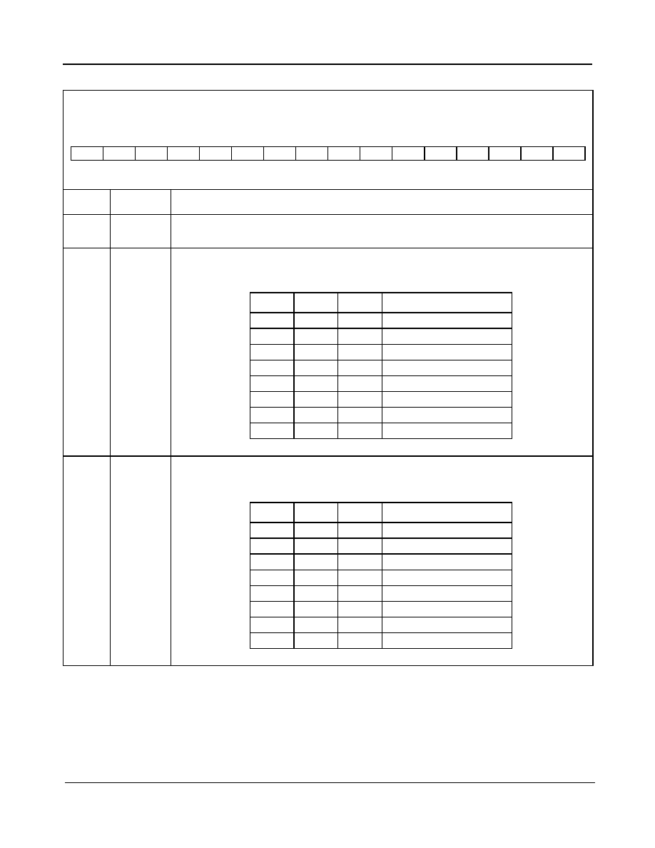
ZL50015
Data Sheet
64
Zarlink Semiconductor Inc.
Bit
Name
Description
15-12
Unused
Reserved
In normal functional mode, these bits MUST be set to zero.
11 - 9
R3F2 - 0
Reference 3 Frequency Bits
When the RFRE bit of the DPLLCR register is high, these bits are used to select the
REF3 input frequency. When the RFRE bit is low, these bits are ignored.
8 - 6
R2F2 - 0
Reference 2 Frequency Bits: When the RFRE bit of the DPLLCR register is high, these
bits are used to select the REF2 input frequency. When the RFRE bit is low, these bits
are ignored.
Table 27 - Reference Frequency Register (RFR) Bits
External Read/Write Address: 0041
H
Reset Value: 0000
H
15
14
13
12
11
10
9
8
7
6
5
4
3
2
1
0
0
0
0
0
R3F2
R3F1
R3F0
R2F2
R2F1
R2F0
R1F2
R1F1
R1F0
R0F2
R0F1
R0F0
R3F2
R3F1
R3F0
REF 3 Input Frequency
0
0
0
8 kHz
0
0
1
1.544 MHz
0
1
0
2.048 MHz
0
1
1
4.096 MHz
1
0
0
8.192 MHz
1
0
1
16.384 MHz
1
1
0
19.44 MHz
1
1
1
Reserved
R2F2
R2F1
R2F0
REF 2 Input Frequency
0
0
0
8 kHz
0
0
1
1.544 MHz
0
1
0
2.048 MHz
0
1
1
4.096 MHz
1
0
0
8.192 MHz
1
0
1
16.384 MHz
1
1
0
19.44 MHz
1
1
1
Reserved

ZL50015
Data Sheet
65
Zarlink Semiconductor Inc.
5 - 3
R1F2 - 0
Reference 1 Frequency Bits
When the RFRE bit of the DPLLCR register is high, these bits are used to select the
REF1 input frequency. When the RFRE bit is low, these bits are ignored.
2 - 0
R0F2 - 0
Reference 0 Frequency Bits
When the RFRE bit of the DPLLCR register is high, these bits are used to select the
REF0 input frequency. When the RFRE bit is low, these bits are ignored.
Bit
Name
Description
Table 27 - Reference Frequency Register (RFR) Bits (continued)
External Read/Write Address: 0041
H
Reset Value: 0000
H
15
14
13
12
11
10
9
8
7
6
5
4
3
2
1
0
0
0
0
0
R3F2
R3F1
R3F0
R2F2
R2F1
R2F0
R1F2
R1F1
R1F0
R0F2
R0F1
R0F0
R1F2
R1F1
R1F0
REF 1 Input Frequency
0
0
0
8 kHz
0
0
1
1.544 MHz
0
1
0
2.048 MHz
0
1
1
4.096 MHz
1
0
0
8.192 MHz
1
0
1
16.384 MHz
1
1
0
19.44 MHz
1
1
1
Reserved
R0F2
R0F1
R0F0
REF 0 Input Frequency
0
0
0
8 kHz
0
0
1
1.544 MHz
0
1
0
2.048 MHz
0
1
1
4.096 MHz
1
0
0
8.192 MHz
1
0
1
16.384 MHz
1
1
0
19.44 MHz
1
1
1
Reserved
ZL50015
Data Sheet
66
Zarlink Semiconductor Inc.
Bit
Name
Description
15 - 0
CFN15 - 0
Center Frequency Number (CFN) Lower 16 Bits: The total binary value of these bits
and the CFRU register bits defines the output center frequency number according to the
following formula:
where, f
OUT
is desired output center frequency, while f
MCLK
is frequency of DPLL master
clock. For given master clock frequency of 100 MHz, and desired output center fre-
quency of 65.536 MHz, the CFN has the value of:
The register contents should be changed only if compensation for input oscillator (or
crystal) frequency offset is required.
e.g., if master clock frequency is off by +20 ppm (100.002 MHz -> 5 times multiplied c20i
of 20.0004 MHz), the CFN should be programmed to be:
The default value of this register SHOULD NOT be changed in any other circumstances.
Table 28 - Centre Frequency Register - Lower 16 Bits (CFRL)
Bit
Name
Description
15 - 10
Unused
Reserved. In normal functional mode, these bits MUST be set to zero.
9 - 0
CFN25 - 16
Center Frequency Number (CFN) Upper 10 Bits: The total binary value of these bits
and the CFRL register bits represents the center frequency number (CFN) explained
under CFRL register bits explanation.
The default value of this register should be changed only if compensation for input oscil-
lator (or crystal) frequency offset is required, and SHOULD NOT be changed in any other
circumstances.
Table 29 - Centre Frequency Register - Upper 10 Bits (CFRU)
External Read/Write Address: 0042
H
Reset Value: 16B1
H
15
14
13
12
11
10
9
8
7
6
5
4
3
2
1
0
CFN
15
CFN
14
CFN
13
CFN
12
CFN
11
CFN
10
CFN
9
CFN
8
CFN
7
CFN
6
CFN
5
CFN
4
CFN
3
CFN
2
CFN
1
CFN
0
f
OUT
CFN
2
26
------------ f
MCLK
◊
=
CFN
2
26
65.536MHz
100MHz
-------------------------------
◊
2
26
0.65536
◊
43980465
29F16B1
H
=
=
=
=
CFN
2
26
65.536MHz
100.002MHz
-----------------------------------
◊
2
26
0.65534689
◊
43979585
29F1341
H
=
=
=
=
External Read/Write Address: 0043
H
Reset Value: 029F
H
15
14
13
12
11
10
9
8
7
6
5
4
3
2
1
0
0
0
0
0
0
0
CFN
25
CFN
24
CFN
23
CFN
22
CFN
21
CFN
20
CFN
19
CFN
18
CFN
17
CFN
16
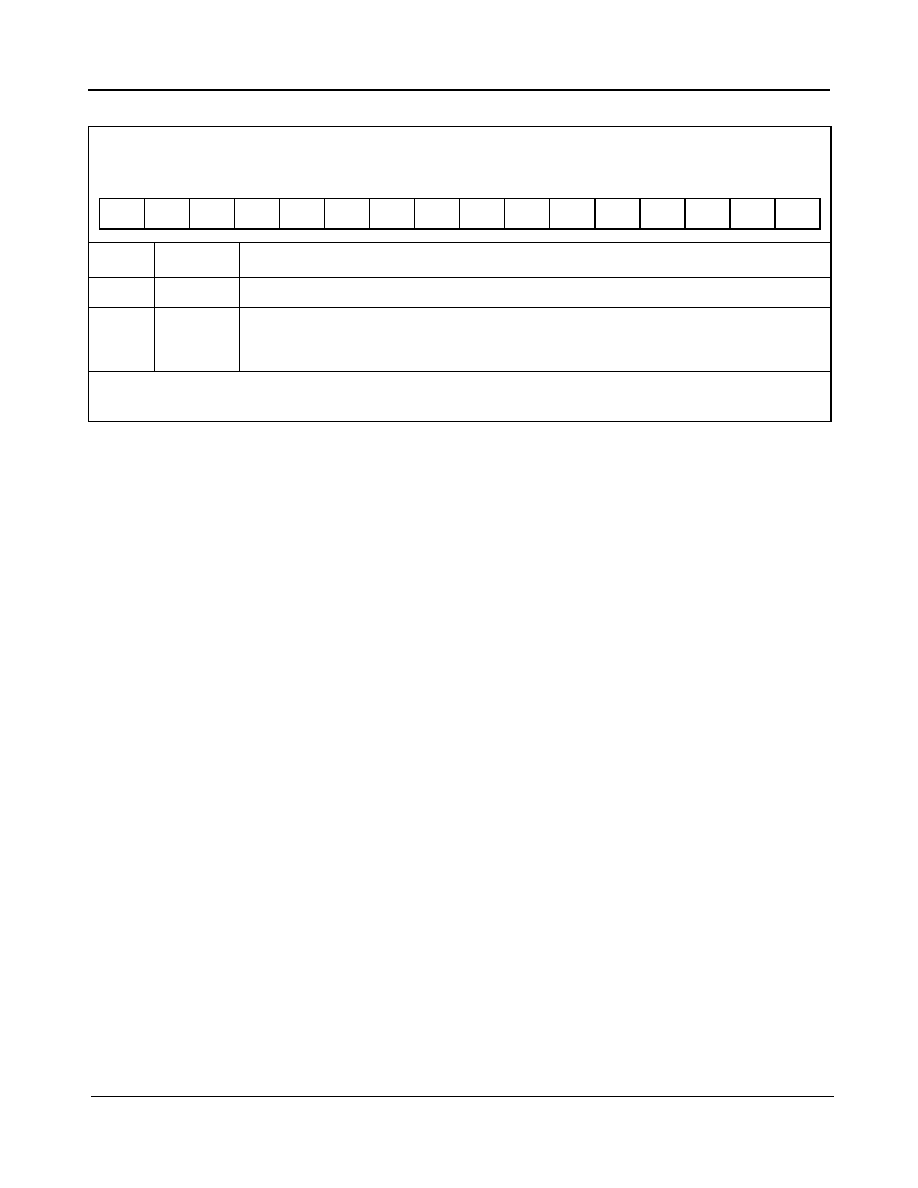
ZL50015
Data Sheet
67
Zarlink Semiconductor Inc.
Bit
Name
Description
15
Unused
Reserved. In normal functional mode, this bit is zero.
14 - 0
FOF14 - 0
Frequency Offset Bits: The binary value of these bits represents the current deviation
of the DPLL output from its center frequency. Defined in same units as CFN in the 2's
complement format.
Note 1: Output frequency offset, relative to master clock, will be represented as the following:
+10 ppm: CFN x 0.00001 = 440 = 01B8
H
-10 ppm: CFN x (-0.00001) = -440 = 7E48
H
Table 30 - Frequency Offset Register (FOR) Bits - Read Only
External Read Only Address: 0045
H
15
14
13
12
11
10
9
8
7
6
5
4
3
2
1
0
0
FOF
14
FOF
13
FOF
12
FOF
11
FOF
10
FOF
9
FOF
8
FOF
7
FOF
6
FOF
5
FOF
4
FOF
3
FOF
2
FOF
1
FOF
0
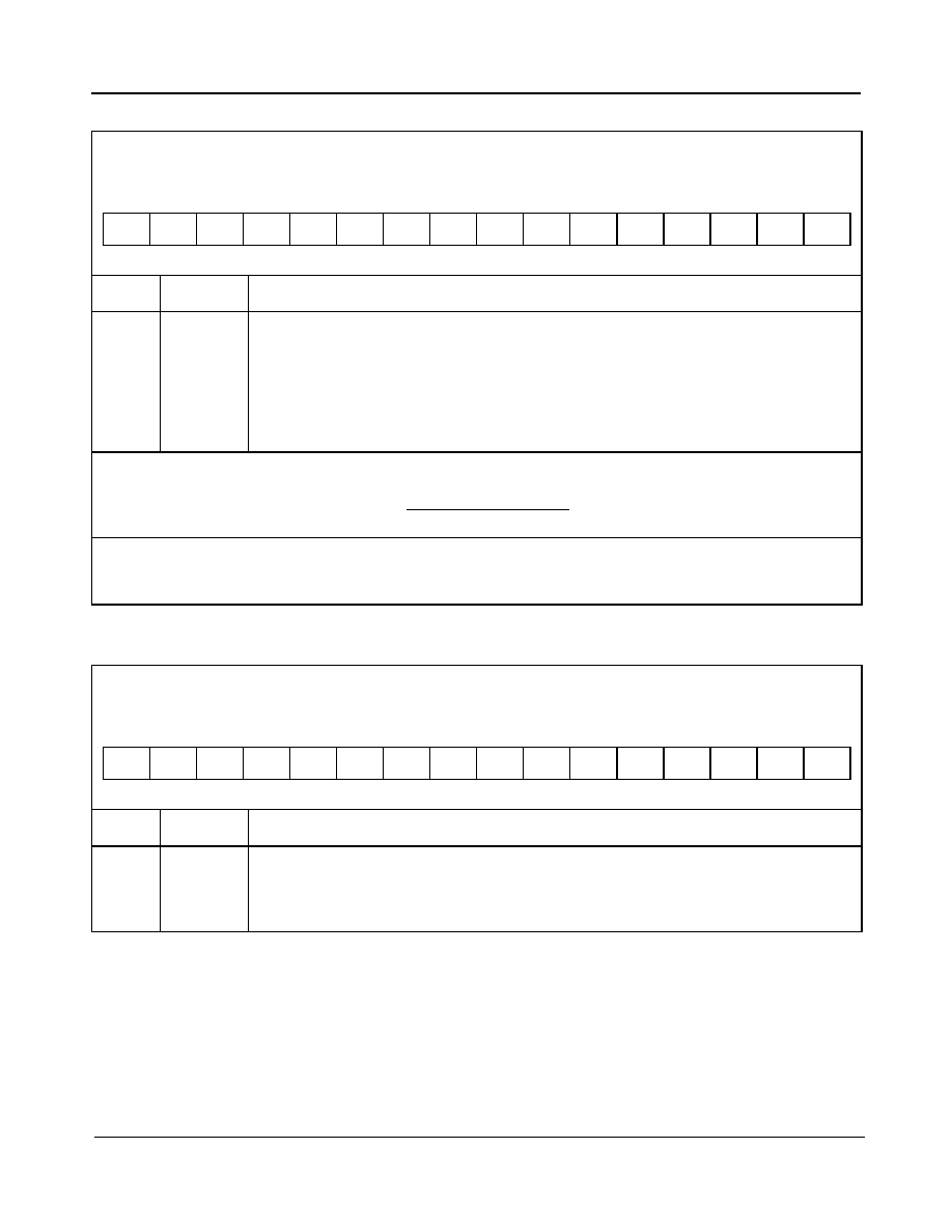
ZL50015
Data Sheet
68
Zarlink Semiconductor Inc.
Table 32 - Lock Detector Interval Register (LDIR) Bits
Bit
Name
Description
15 - 0
LDT15 - 0
Lock Detect Threshold Bits
The binary value of these bits defines the upper limit of the absolute phase from the
phase detector output for lock detection.
When the value of the absolute phase is less than or equal to LDT for duration of time
defined by the LDIR register, the DPLL locks.
When the value of the absolute phase is greater than LDT for duration of time defined by
the LDIR register divided by 256, the DPLL does not lock.
Note: LDT should be calculated as per the maximum expected amplitude of jitter on the active input reference
using the following formula:
LDT = MAX_EXP_JITTER (ns) x 2
15.2 (ns)
Example: If maximum expected jitter amplitude on 2.048 MHz reference is 10UI (i.e., 10 x 488.2 ns = 4882 ns)
(assuming the jitter frequency where DPLL attenuation is big), the LDT should be programmed to be (4882/15.2)
x 2 = 642 = 0282
H
Table 31 - Lock Detector Threshold Register (LDTR) Bits
Bit
Name
Description
15 - 0
LDI15 - 0
Lock Detector Interval Bits
The binary value of these bits defines the time interval that the output phase detector
must be below the lock detect threshold to declare lock. Unsigned representation of the
LDI bits is defined in 4 ms intervals.
External Read/Write Address: 0047
H
Reset Value: 000F
H
15
14
13
12
11
10
9
8
7
6
5
4
3
2
1
0
LDT
15
LDT
14
LDT
13
LDT
12
LDT
11
LDT
10
LDT
9
LDT
8
LDT
7
LDT
6
LDT
5
LDT
4
LDT
3
LDT
2
LDT
1
LDT
0
External Read/Write Address: 0048
H
Reset Value: 2C00
H
15
14
13
12
11
10
9
8
7
6
5
4
3
2
1
0
LDI
15
LDI
14
LDI
13
LDI
12
LDI
11
LDI
10
LDI
9
LDI
8
LDI
7
LDI
6
LDI
5
LDI
4
LDI
3
LDI
2
LDI
1
LDI
0
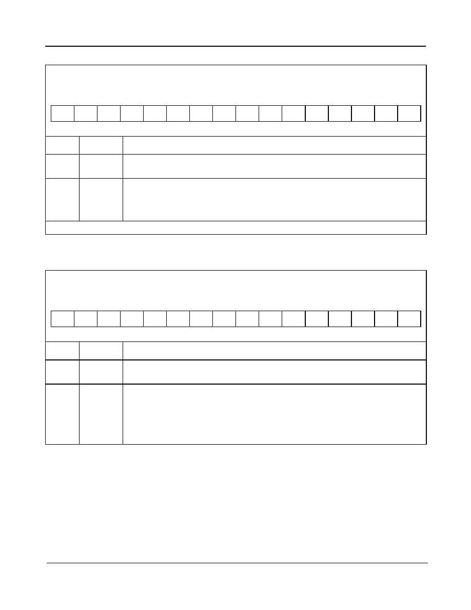
ZL50015
Data Sheet
69
Zarlink Semiconductor Inc.
Bit
Name
Description
15 - 13
Unused
Reserved
In normal functional mode, these bits MUST be set to zero.
12 - 0
SRL12 - 0
Slew Rate Limit Bits
The binary value of these bits defines the maximum rate of DPLL phase change (phase
slope), where the phase represents difference between the input reference and output
feedback clock. Defined in same units as CFN (unsigned).
Note: The default value is
±56 ppm ('h099F/CFN = 56 ppm).
Table 33 - Slew Rate Limit Register (SRLR) Bits
Bit
Name
Description
15 - 8
Unused
Reserved
In normal functional mode, these bits MUST be set to zero.
7
MTR
MTIE Reset
When this bit is low, the MTIE circuit applies a phase offset between the reference input
clock and the DPLL output clock and the phase offset value is maintained. When this bit
is high, MTIE circuit is in its reset state and the phase offset value is reset to zero,
causing alignment of the DPLL output clocks to nearest edge of the selected input
reference.
Table 34 - Reference Change Control Register (RCCR) Bits
External Read/Write Address: 0049
H
Reset Value: 099F
H
(see Note)
15
14
13
12
11
10
9
8
7
6
5
4
3
2
1
0
0
0
0
SRL
12
SRL
11
SRL
10
SRL
9
SRL
8
SRL
7
SRL
6
SRL
5
SRL
4
SRL
3
SRL
2
SRL
1
SRL
0
External Read/Write Address: 004B
H
Reset Value: 0000
H
15
14
13
12
11
10
9
8
7
6
5
4
3
2
1
0
0
0
0
0
0
0
0
0
MTR
PRS
1
PRS
0
PMS
2
PMS
1
PMS
0
FDM
1
FDM
0

ZL50015
Data Sheet
70
Zarlink Semiconductor Inc.
6 - 5
PRS1 - 0
Preferred Reference Selection Bits
These bits select the preferred reference from one of the input references. They are used
only if the PMS2-0 bits are set to 001. Otherwise, these bits are ignored
4 - 2
PMS2 - 0
Preference Mode Selection Bits
These bits select one of the preference modes:
If in automatic mode with a preferred reference (PMS2-0 = 001 and FDM1-0 = 00), the
automatic state machine will only switch between two references (as per Table 8). Please
see Section 12.1.3.2, "Automatic Reference Switching With Preferences" on page 40 for
more details.
1 - 0
FDM1 - 0
Force DPLL Timing Mode
These bits force the DPLL into one of the valid operation modes.
Bit
Name
Description
Table 34 - Reference Change Control Register (RCCR) Bits (continued)
External Read/Write Address: 004B
H
Reset Value: 0000
H
15
14
13
12
11
10
9
8
7
6
5
4
3
2
1
0
0
0
0
0
0
0
0
0
MTR
PRS
1
PRS
0
PMS
2
PMS
1
PMS
0
FDM
1
FDM
0
PRS1
PRS0
Preferred Reference Selection
0
0
REF0
0
1
REF1
1
0
REF2
1
1
REF3
PMS2
PMS1
PMS0
Preference Mode
0
0
0
No Preference
0
0
1
Preference as per the setting
of the PRS1 - 0 bits
0
1
0
Force REF0
0
1
1
Force REF1
1
0
0
Force REF2
1
0
1
Force REF3
110 - 111
Reserved
FDM1
FDM0
DPLL TIMING Mode
0
0
Automatic
0
1
Normal
1
0
Holdover
1
1
Freerun
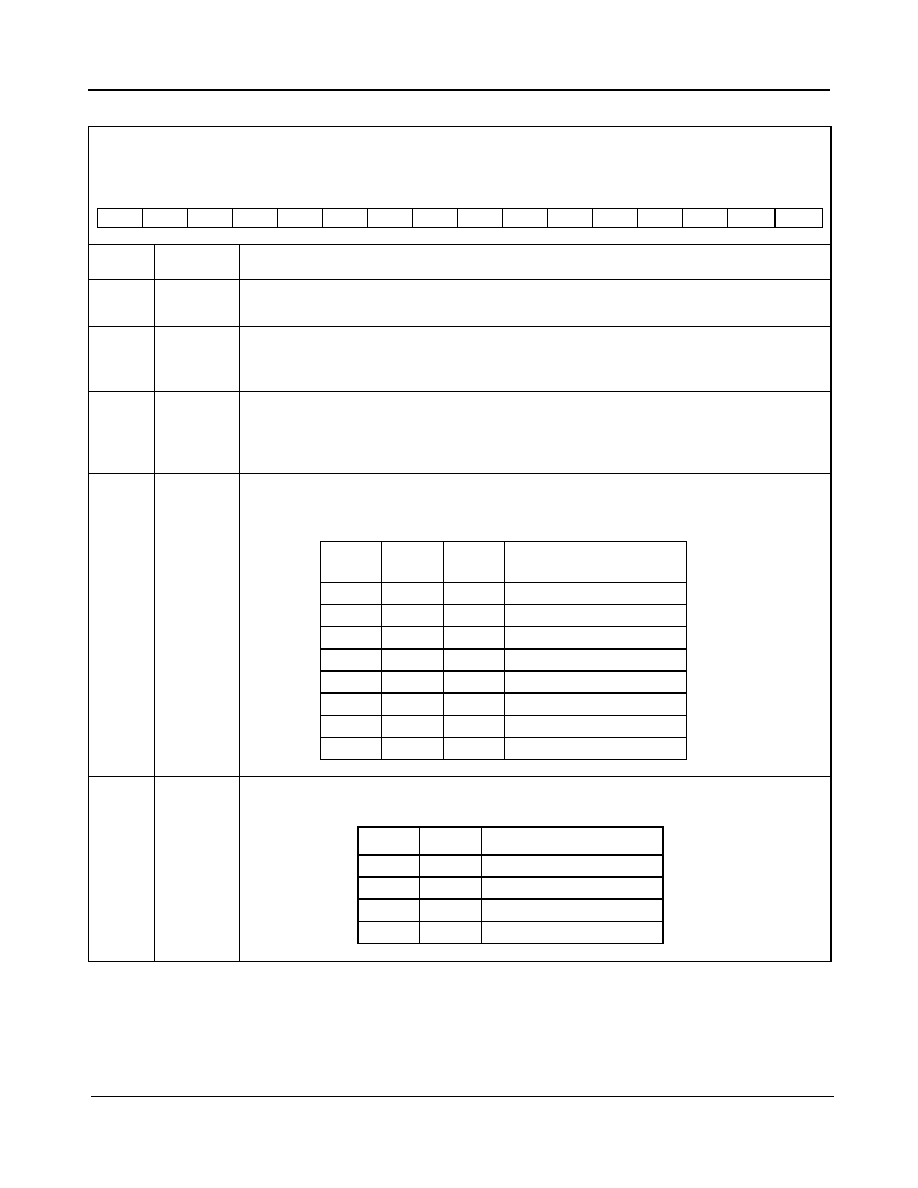
ZL50015
Data Sheet
71
Zarlink Semiconductor Inc.
Bit
Name
Description
15 - 9
Unused
Reserved
In normal functional mode, these bits are zero.
8
SLM
Slew Rate Limiter Status Bit
If the device sets this bit to high, the DPLL phase difference between the input and output
clocks is changing at the slew rate limit defined in the Slew Rate Limit Register (SRLR).
7
LST
Lock Status Bit
If the device sets this bit to high, while the LDTR and LDIR registers are programmed
properly, the DPLL output clocks are locked to the selected input reference.
If this bit is low, the DPLL output clocks are not yet locked to the selected input reference.
6 - 4
RFR2 - 0
Reference Frequency Indicator Bits
These bits represent the frequency of the selected reference indicated by the reference
bits (RES1 - 0) in this register.
3 - 2
RES1 - 0
Reference Select Indicator Bits: These bits indicate which one of the four reference
inputs (REF0 - 3 pins) is being selected by the device.
Table 35 - Reference Change Status Register (RCSR) Bits - Read Only
External Read Only Address: 004C
H
15
14
13
12
11
10
9
8
7
6
5
4
3
2
1
0
0
0
0
0
0
0
0
SLM
LST
RFR2
RFR1
RFR0
RES1
RES0
DPM1
DPM0
RFR2
RFR1
RFR0
Frequency of the Selected
Reference
0
0
0
8 kHz
0
0
1
1.544 MHz
0
1
0
2.048 MHz
0
1
1
4.096 MHz
1
0
0
8.192 MHz
1
0
1
16.384 MHz
1
1
0
19.44 MHz
1
1
1
Reserved
RES1
RES0
Input Reference in use
0
0
REF 0
0
1
REF 1
1
0
REF 2
1
1
REF 3
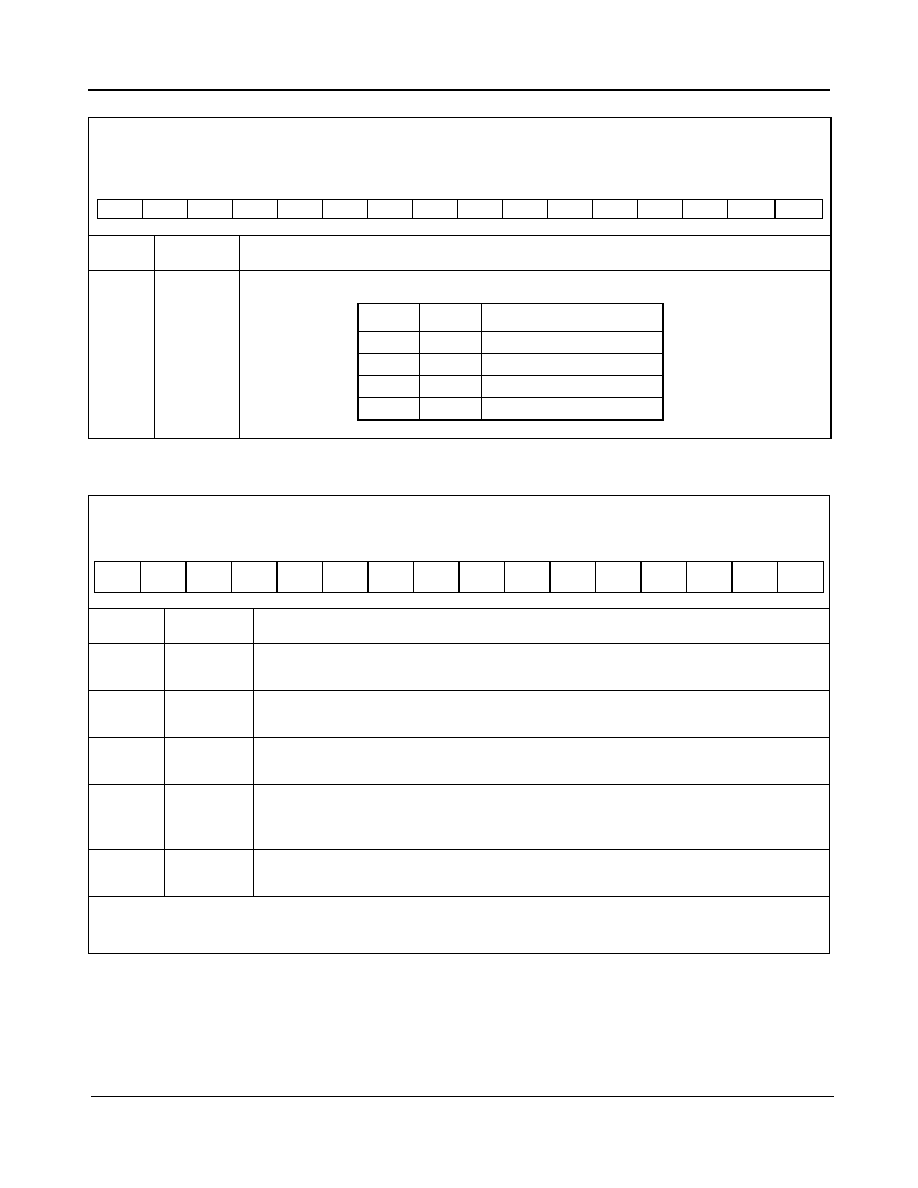
ZL50015
Data Sheet
72
Zarlink Semiconductor Inc.
1 - 0
DPM1 - 0
DPLL Timing Mode Status Bits: These bits indicate the DPLL's timing mode status.
Bit
Name
Description
15 - 4
Unused
Reserved
In normal functional mode, these bits is zero.
3
LCI
Lock Change Interrupt Bit
If the device sets this bit to high, the device lock status has changed.
2
RCI
Reference Change Interrupt Bit
If the device sets this bit to high, the selected reference has changed.
1
HOI
Holdover Interrupt Bit
If the device sets this bit to high, the device has entered or recovered from the
holdover/MTIE mode.
0
Unused
Reserved
In normal functional mode, this bit is zero.
Note 1: If any of these bits are set, the interrupt output will become active unless the Interrupt Mask Register (IMR) has a high
value for that particular bit.
Note 2: Any of these bits can be cleared by setting the appropriate bit in the Interrupt Clear Register.
Table 36 - Interrupt Register (IR) Bits - Read Only
Bit
Name
Description
Table 35 - Reference Change Status Register (RCSR) Bits - Read Only (continued)
External Read Only Address: 004C
H
15
14
13
12
11
10
9
8
7
6
5
4
3
2
1
0
0
0
0
0
0
0
0
SLM
LST
RFR2
RFR1
RFR0
RES1
RES0
DPM1
DPM0
DPM1
DPM0
DPLL
Timing Mode State
0
0
MTIE
0
1
Normal
1
0
Holdover
1
1
Freerun
External Read Only Address: 0066
H
15
14
13
12
11
10
9
8
7
6
5
4
3
2
1
0
0
0
0
0
0
0
0
0
0
0
0
0
LCI
RCI
HOI
0
ZL50015
Data Sheet
73
Zarlink Semiconductor Inc.
Bit
Name
Description
15 - 4
Unused
Reserved
In normal functional mode, these bits MUST be set to zero.
3
LIM
Lock Interrupt Mask Bit
When this bit is high, it masks the lock status change interrupt.
2
RIM
Reference Change Interrupt Mask Bit
When this bit is high, it masks the reference change interrupt.
1
HIM
Holdover Interrupt Mask Bit
When this bit is high, it masks the holdover entry/exit interrupt.
0
Unused
Reserved
In normal functional mode, this bit MUST be set to one.
Table 37 - Interrupt Mask Register (IMR) Bits
Bit
Name
Description
15 - 4
Unused
Reserved
In normal functional mode, these bits MUST be set to zero.
3 - 1
ICB3 - 1
Interrupt Clear Bits
Writing a "1" to any bit in this register will clear the corresponding bit in the Interrupt
Register (IR). The Interrupt Clear Register is self-clearing, i.e. once it has completed
its action, the ICR register bit returns to 0.
0
Unused
Reserved
In normal functional mode, this bit MUST be set to one.
Table 38 - Interrupt Clear Register (ICR) Bits
External Read/Write Address: 0067
H
Reset Value: 000F
H
15
14
13
12
11
10
9
8
7
6
5
4
3
2
1
0
0
0
0
0
0
0
0
0
0
0
0
0
LIM
RIM
HIM
1
External Read/Write Address: 0068
H
Reset Value: 0000
H
15
14
13
12
11
10
9
8
7
6
5
4
3
2
1
0
0
0
0
0
0
0
0
0
0
0
0
0
ICB
3
ICB
2
ICB
1
1

ZL50015
Data Sheet
74
Zarlink Semiconductor Inc.
Bit
Name
Description
15
R3FML
Reference 3 Multi-period Lower Limit Fail Bit
f the device sets this bit to high, the input REF3 fails the multi-period lower limit check.
(See Table 12, "Multi-Period Hysteresis Limits" on page 45)
14
R3FMU
Reference 3 Multi-period Upper Limit Fail Bit
If the device sets this bit to high, the input REF3 fails the multi-period upper limit
check. (See Table 12, "Multi-Period Hysteresis Limits" on page 45)
13
R3FL
Reference 3 Single Period Lower Limit Fail Bit
If the device sets this bit to high, the input REF3 fails the single-period lower limit
check. (See Table 11, "Values for Single Period Limits" on page 45)
12
R3FU
Reference 3 Single Period Upper Limit Fail Bit
If the device sets this bit to high, the input REF3 fails the single-period upper limit
check. (See Table 11, "Values for Single Period Limits" on page 45)
11
R2FML
Reference 2 Multi-period Lower Limit Fail Bit
If the device sets this bit to high, the input REF2 fails the multi-period lower limit check.
(See Table 12, "Multi-Period Hysteresis Limits" on page 45)
10
R2FMU
Reference 2 Multi-period Upper Limit Fail Bit
If the device sets this bit to high, the input REF2 fails the multi-period upper limit
check. (See Table 12, "Multi-Period Hysteresis Limits" on page 45)
9
R2FL
Reference 2 Single Period Lower Limit Fail Bit
If the device sets this bit to high, the input REF2 fails the single-period lower limit
check. (See Table 11, "Values for Single Period Limits" on page 45)
8
R2FU
Reference 2 Single Period Upper Limit Fail Bit
If the device sets this bit to high, the input REF2 fails the single-period upper limit
check.(see Table 11, "Values for Single Period Limits" on page 45)
7
R1FML
Reference 1 Multi-period Lower Limit Fail Bit
If the device sets this bit to high, the input REF1 fails the multi-period lower limit check.
(See Table 12, "Multi-Period Hysteresis Limits" on page 45)
6
R1FMU
Reference 1 Multi-period Upper Limit Fail Bit
If the device sets this bit to high, the input REF1 fails the multi-period upper limit
check. (See Table 12, "Multi-Period Hysteresis Limits" on page 45)
5
R1FL
Reference 1 Single Period Lower Limit Fail Bit
If the device sets this bit to high, the input REF1 fails the single-period lower limit
check. (See Table 11, "Values for Single Period Limits" on page 45)
Table 39 - Reference Failure Status Register (RSR) Bits - Read Only
External Read Only Address: 0069
H
15
14
13
12
11
10
9
8
7
6
5
4
3
2
1
0
R3
FML
R3
FMU
R3
FL
R3
FU
R2
FML
R2
FMU
R2
FL
R2
FU
R1
FML
R1
FMU
R1
FL
R1
FU
R0
FML
R0
FMU
R0
FL
R0
FU
ZL50015
Data Sheet
75
Zarlink Semiconductor Inc.
4
R1FU
Reference 1 Single Period Upper Limit Fail Bit
If the device sets this bit to high, the input REF1 fails the single-period upper limit
check. (See Table 11, "Values for Single Period Limits" on page 45)
3
R0FML
Reference 0 Multi-period Lower Limit Fail Bit
If the device sets this bit to high, the input REF0 fails the multi-period lower limit check.
(See Table 12, "Multi-Period Hysteresis Limits" on page 45)
2
R0FMU
Reference 0 Multi-period Upper Limit Fail Bit
If the device sets this bit to high, the input REF0 fails the multi-period upper limit
check. (See Table 12, "Multi-Period Hysteresis Limits" on page 45)
1
R0FL
Reference 0 Single Period Lower Limit Fail Bit
If the device sets this bit to high, the input REF0 fails the single-period lower limit
check. (See Table 11, "Values for Single Period Limits" on page 45)
0
R0FU
Reference 0 Single Period Upper Limit Fail Bit
If the device sets this bit to high, the input REF0 fails the single-period upper limit
check. (See Table 11, "Values for Single Period Limits" on page 45)
Bit
Name
Description
15
R3MML
Reference 3 Multi-period Lower Limit Mask Bit
When this bit is high, it masks the multi-period lower limit check (or forces pass) for
REF3.
14
R3MMU
Reference 3 Multi-period Upper Limit Mask Bit
When this bit is high, it masks the multi-period upper limit check (or forces pass) for
REF3.
13
R3ML
Reference 3 Single-period Lower Limit Mask Bit
When this bit is high, it masks the single-period lower limit check (or forces pass) for
REF3.
Table 40 - Reference Mask Register (RMR) Bits
Bit
Name
Description
Table 39 - Reference Failure Status Register (RSR) Bits - Read Only (continued)
External Read Only Address: 0069
H
15
14
13
12
11
10
9
8
7
6
5
4
3
2
1
0
R3
FML
R3
FMU
R3
FL
R3
FU
R2
FML
R2
FMU
R2
FL
R2
FU
R1
FML
R1
FMU
R1
FL
R1
FU
R0
FML
R0
FMU
R0
FL
R0
FU
External Read/Write Address: 006A
H
Reset Value: 0000
H
15
14
13
12
11
10
9
8
7
6
5
4
3
2
1
0
R3
MML
R3
MMU
R3
ML
R3
MU
R2
MML
R2
MMU
R2
ML
R2
MU
R1
MML
R1
MMU
R1
ML
R1
MU
R0
MML
R0
MMU
R0
ML
R0
MU

ZL50015
Data Sheet
76
Zarlink Semiconductor Inc.
12
R3MU
Reference 3 Single-period Upper Limit Mask Bit
When this bit is high, it masks the single-period upper limit check (or forces pass) for
REF3.
11
R2MML
Reference 2 Multi-period Lower Limit Mask Bit
When this bit is high, it masks the multi-period lower limit check (or forces pass) for
REF2.
10
R2MMU
Reference 2 Multi-period Upper Limit Mask Bit
When this bit is high, it masks the multi-period upper limit check (or forces pass) for
REF2.
9
R2ML
Reference 2 Single-period Lower Limit Mask Bit
When this bit is high, it masks the single-period lower limit check (or forces pass) for
REF2.
8
R2MU
Reference 2 Single-period Upper Limit Mask Bit
When this bit is high, it masks the single-period upper limit check (or forces pass) for
REF2.
7
R1MML
Reference 1 Multi-period Lower Limit Mask Bit
When this bit is high, it masks the multi-period lower limit check (or forces pass) for
REF1.
6
R1MMU
Reference 1 Multi-period Upper Limit Mask Bit
When this bit is high, it masks the multi-period upper limit check (or forces pass) for
REF1.
5
R1ML
Reference 1 Single-period Lower Limit Mask Bit
When this bit is high, it masks the single-period lower limit check (or forces pass) for
REF1.
4
R1MU
Reference 1 Single-period Upper Limit Mask Bit
When this bit is high, it masks the single-period upper limit check (or forces pass) for
REF1.
3
R0MML
Reference 0 Multi-period Lower Limit Mask Bit
When this bit is high, it masks the multi-period lower limit check (or forces pass) for
REF0.
2
R0MMU
Reference 0 Multi-period Upper Limit Mask Bit
When this bit is high, it masks the multi-period upper limit check (or forces pass) for
REF0.
Bit
Name
Description
Table 40 - Reference Mask Register (RMR) Bits (continued)
External Read/Write Address: 006A
H
Reset Value: 0000
H
15
14
13
12
11
10
9
8
7
6
5
4
3
2
1
0
R3
MML
R3
MMU
R3
ML
R3
MU
R2
MML
R2
MMU
R2
ML
R2
MU
R1
MML
R1
MMU
R1
ML
R1
MU
R0
MML
R0
MMU
R0
ML
R0
MU
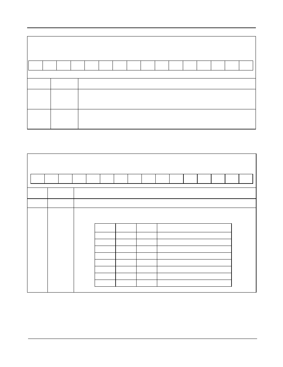
ZL50015
Data Sheet
77
Zarlink Semiconductor Inc.
1
R0ML
Reference 0 Single-period Lower Limit Mask Bit
When this bit is high, it masks the single-period lower limit check (or forces pass) for
REF0.
0
R0MU
Reference 0 Single-period Upper Limit Mask Bit
When this bit is high, it masks the single-period upper limit check (or forces pass) for
REF0.
Bit
Name
Description
15 - 12
Unused
Reserved. In normal functional mode, these bits are zero.
11 - 9
R3FS2 - 0
Reference 3 Frequency Status Bits
These bits report detected frequency of REF3.
Table 41 - Reference Frequency Status Register (RFSR) Bits - Read only
Bit
Name
Description
Table 40 - Reference Mask Register (RMR) Bits (continued)
External Read/Write Address: 006A
H
Reset Value: 0000
H
15
14
13
12
11
10
9
8
7
6
5
4
3
2
1
0
R3
MML
R3
MMU
R3
ML
R3
MU
R2
MML
R2
MMU
R2
ML
R2
MU
R1
MML
R1
MMU
R1
ML
R1
MU
R0
MML
R0
MMU
R0
ML
R0
MU
External Read Only Address: 006B
H
15
14
13
12
11
10
9
8
7
6
5
4
3
2
1
0
0
0
0
0
R3FS
2
R3FS
1
R3FS
0
R2FS
2
R2FS
1
R2FS
0
R1FS
2
R1FS
1
R1FS
0
R0FS
2
R0FS
1
R0FS
0
R3FS2
R3FS1
R3FS0
REF3 Frequency Measurement
0
0
0
8 kHz
0
0
1
1.544 MHz
0
1
0
2.048 MHz
0
1
1
4.096 MHz
1
0
0
8.192 MHz
1
0
1
16.384 MHz
1
1
0
19.44 MHz
1
1
1
Reserved
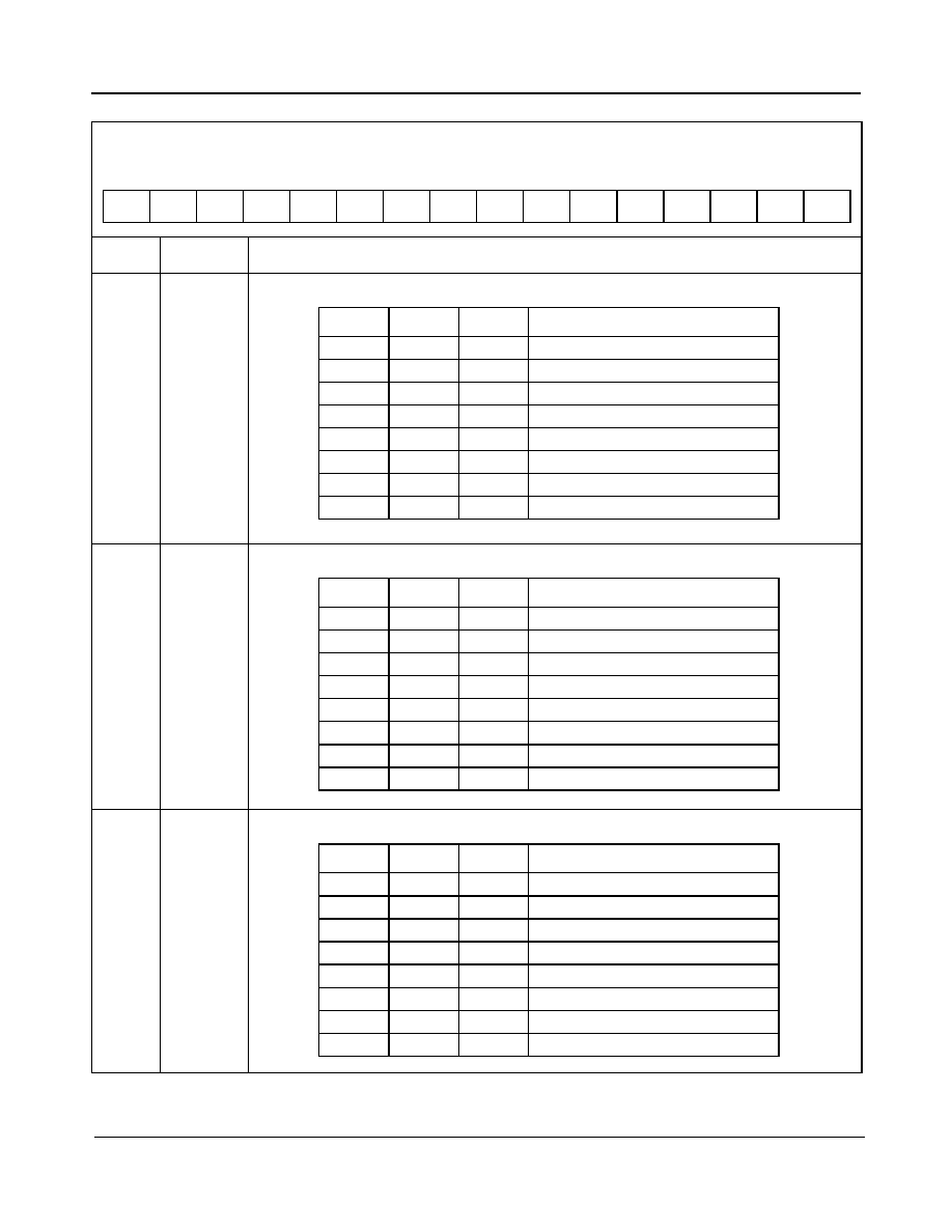
ZL50015
Data Sheet
78
Zarlink Semiconductor Inc.
8 - 6
R2FS2 - 0
Reference 2 Frequency Status Bits: These bits report detected frequency of REF2.
5 - 3
R1FS2 - 0
Reference 1 Frequency Status Bits: These bits report detected frequency of REF1.
2 - 0
R0FS2 - 0
Reference 0 Frequency Status Bits: These bits report detected frequency of REF0.
Bit
Name
Description
Table 41 - Reference Frequency Status Register (RFSR) Bits - Read only (continued)
External Read Only Address: 006B
H
15
14
13
12
11
10
9
8
7
6
5
4
3
2
1
0
0
0
0
0
R3FS
2
R3FS
1
R3FS
0
R2FS
2
R2FS
1
R2FS
0
R1FS
2
R1FS
1
R1FS
0
R0FS
2
R0FS
1
R0FS
0
R2FS2
R2FS1
R2FS0
REF 2 Frequency Measurement
0
0
0
8 kHz
0
0
1
1.544 MHz
0
1
0
2.048 MHz
0
1
1
4.096 MHz
1
0
0
8.192 MHz
1
0
1
16.384 MHz
1
1
0
19.44 MHz
1
1
1
Reserved
R1FS2
R1FS1
R1FS0
REF1 Frequency Measurement
0
0
0
8 kHz
0
0
1
1.544 MHz
0
1
0
2.048 MHz
0
1
1
4.096 MHz
1
0
0
8.192 MHz
1
0
1
16.384 MHz
1
1
0
19.44 MHz
1
1
1
Reserved
R0FS2
R0FS1
R0FS0
REF 0 Frequency Measurement
0
0
0
8 kHz
0
0
1
1.544 MHz
0
1
0
2.048 MHz
0
1
1
4.096 MHz
1
0
0
8.192 MHz
1
0
1
16.384 MHz
1
1
0
19.44 MHz
1
1
1
Reserved
ZL50015
Data Sheet
79
Zarlink Semiconductor Inc.
Bit
Name
Description
15 - 3
Unused
Reserved
In normal functional mode, these bits MUST be set to zero.
2 - 0
OJP2 - 0
Output Jitter Performance Bits
These bits are used to control the DPLL output jitter performance with respect to the
noise received through the output pins. The higher value (unsigned) means more
filtering, while zero means filter bypass. The default value of 2
H
gives the best
performance for most circumstances.
Table 42 - Output Jitter Control Register (OJCR) Bits
Bit
Name
Description
15 - 9
Unused
Reserved
In normal functional mode, these bits MUST be set to zero
.
8 - 6
STIN[n]BD2 - 0
Input Stream[n] Bit Delay Bits.
The binary value of these bits refers to the number of bits that the input stream
will be delayed relative to FPi. The maximum value is 7. Zero means no delay.
5 - 4
STIN[n]SMP1 - 0
Input Data Sampling Point Selection Bits
Table 43 - Stream Input Control Register 0 - 15 (SICR0 - 15) Bits
External Read/Write Address: 006C
H
Reset Value: 0002
H
15
14
13
12
11
10
9
8
7
6
5
4
3
2
1
0
0
0
0
0
0
0
0
0
0
0
0
0
0
OJP2
OJP1
OJP0
External Read/Write Address: 0100
H
- 010F
H
Reset Value: 0000
H
15
14
13
12
11
10
9
8
7
6
5
4
3
2
1
0
0
0
0
0
0
0
0
STIN[n]
BD2
STIN[n]
BD1
STIN[n]
BD0
STIN[n]
SMP1
STIN[n]
SMP0
STIN[n]
DR3
STIN[n]
DR2
STIN[n]
DR1
STIN[n]
DR0
STIN[n]SMP1-0
Sampling Point
(2.048 Mbps, 4.096 Mbps, 8.192 Mbps
streams)
Sampling Point
(16.384 Mbps
streams)
00
3/4 point
2/4 point
01
1/4 point
10
2/4 point
4/4 point
11
4/4 point
ZL50015
Data Sheet
80
Zarlink Semiconductor Inc.
3 - 0
STIN[n]DR3 - 0
Input Data Rate Selection Bits:
Note: [n] denotes input stream from 0 - 15.
Bit
Name
Description
Table 43 - Stream Input Control Register 0 - 15 (SICR0 - 15) Bits (continued)
External Read/Write Address: 0100
H
- 010F
H
Reset Value: 0000
H
15
14
13
12
11
10
9
8
7
6
5
4
3
2
1
0
0
0
0
0
0
0
0
STIN[n]
BD2
STIN[n]
BD1
STIN[n]
BD0
STIN[n]
SMP1
STIN[n]
SMP0
STIN[n]
DR3
STIN[n]
DR2
STIN[n]
DR1
STIN[n]
DR0
STIN[n]DR3-0
Data Rate
0000
Stream Unused
0001
2.048 Mbps
0010
4.096 Mbps
0011
8.192 Mbps
0100
16.384 Mbps
0101 - 1111
Reserved
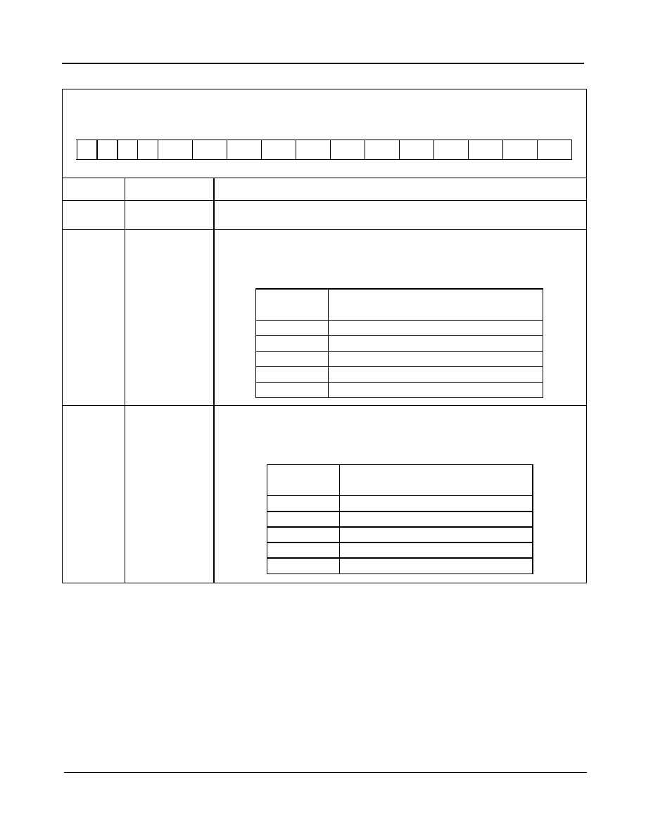
ZL50015
Data Sheet
81
Zarlink Semiconductor Inc.
Bit
Name
Description
15 - 12
Unused
Reserved
In normal functional mode, these bits MUST be set to zero.
11 - 9
STIN[n]Q3C2 - 0
Quadrant Frame 3 Control Bits
These three bits are used to control STi[n]'s quadrant frame 3, which is defined
as Ch24 to 31, Ch48 to 63, Ch96 to 127 and Ch192 to 255 for the 2.048 Mbps,
4.096 Mbps, 8.192 Mbps, and 16.384 Mbps modes respectively.
8 - 6
STIN[n]Q2C2 - 0
Quadrant Frame 2 Control Bits
These three bits are used to control STi[n]'s quadrant frame 2, which is defined
as Ch16 to 23, Ch32 to 47, Ch64 to 95 and Ch128 to 191 for the 2.048 Mbps,
4.096 Mbps, 8.192 Mbps, and 16.384 Mbps modes respectively.
Table 44 - Stream Input Quadrant Frame Register 0 - 15 (SIQFR0 - 15) Bits
External Read/Write Address: 0120
H
- 012F
H
Reset Value: 0000
H
15
14
13
12
11
10
9
8
7
6
5
4
3
2
1
0
0
0
0
0
STIN[n]
Q3C2
STIN[n]
Q3C1
STIN[n]
Q3C0
STIN[n]
Q2C2
STIN[n]
Q2C1
STIN[n]
Q2C0
STIN[n]
Q1C2
STIN[n]
Q1C1
STIN[n]
Q1C0
STIN[n]
Q0C2
STIN[n]
Q0C1
STIN[n]
Q0C0
STIN[n]Q3C
2-0
Operation
0xx
normal operation
100
LSB of each channel is replaced by "0"
101
LSB of each channel is replaced by "1"
110
MSB of each channel is replaced by "0"
111
MSB of each channel is replaced by "1"
STIN[n]Q2C
2-0
Operation
0xx
normal operation
100
LSB of each channel is replaced by "0"
101
LSB of each channel is replaced by "1"
110
MSB of each channel is replaced by "0"
111
MSB of each channel is replaced by "1"
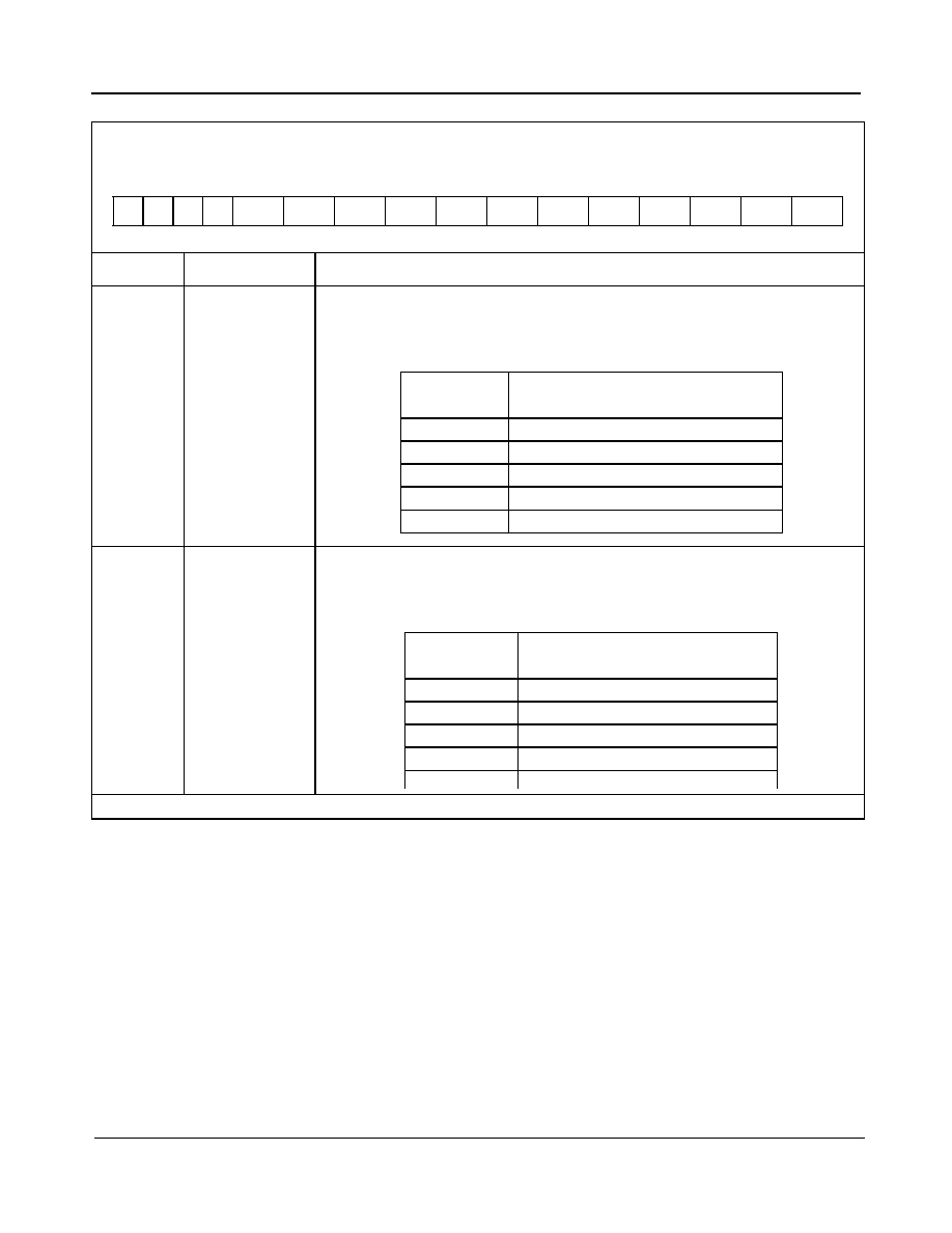
ZL50015
Data Sheet
82
Zarlink Semiconductor Inc.
5 - 3
STIN[n]Q1C2 - 0
Quadrant Frame 1 Control Bits
these three bits are used to control STi[n]'s quadrant frame 1, which is defined
as Ch8 to 15, Ch16 to 31, Ch32 to 63 and Ch64 to 127 for the 2.048 Mbps,
4.096 Mbps, 8.192 Mbps, and 16.384 Mbps modes respectively.
2 - 0
STIN[n]Q0C2 - 0
Quadrant Frame 0 Control Bits
These three bits are used to control STi[n]'s quadrant frame 0, which is defined
as Ch0 to 7, Ch0 to 15, Ch0 to 31 and Ch0 to 63 for the 2.048 Mbps,
4.096 Mbps, 8.192 Mbps, and 16.384 Mbps modes respectively.
Note: [n] denotes input stream from 0 - 15.
Bit
Name
Description
Table 44 - Stream Input Quadrant Frame Register 0 - 15 (SIQFR0 - 15) Bits (continued)
External Read/Write Address: 0120
H
- 012F
H
Reset Value: 0000
H
15
14
13
12
11
10
9
8
7
6
5
4
3
2
1
0
0
0
0
0
STIN[n]
Q3C2
STIN[n]
Q3C1
STIN[n]
Q3C0
STIN[n]
Q2C2
STIN[n]
Q2C1
STIN[n]
Q2C0
STIN[n]
Q1C2
STIN[n]
Q1C1
STIN[n]
Q1C0
STIN[n]
Q0C2
STIN[n]
Q0C1
STIN[n]
Q0C0
STIN[n]Q1C
2-0
Operation
0xx
normal operation
100
LSB of each channel is replaced by "0"
101
LSB of each channel is replaced by "1"
110
MSB of each channel is replaced by "0"
111
MSB of each channel is replaced by "1"
STIN[n]Q0C
2-0
Operation
0xx
normal operation
100
LSB of each channel is replaced by "0"
101
LSB of each channel is replaced by "1"
110
MSB of each channel is replaced by "0"
111
MSB of each channel is replaced by "1"

ZL50015
Data Sheet
83
Zarlink Semiconductor Inc.
Bit
Name
Description
15 - 12
Unused
Reserved
In normal functional mode, these bits MUST be set to zero.
11 - 9
STOHZ[n]A2 - 0
(Valid only for STio0-7)
STOHZ Additional Advancement Bits
8 - 7
STO[n]FA1 - 0
Output Stream[n] Fractional Advancement Bits
6 - 4
STO[n]AD2 - 0
Output Stream[n] Bit Advancement Selection Bits
The binary value of these bits refers to the number of bits that the output stream
is to be advanced relative to FPo. The maximum value is 7. Zero means no
advancement.
3 - 0
STO[n]DR3 - 0
Output Data Rate Selection Bits
Note: [n] denotes output stream from 0 - 15.
Table 45 - Stream Output Control Register 0 - 15 (SOCR0 - 15) Bits
External Read/Write Address: 0200
H
- 020F
H
Reset Value: 0000
H
15
14
13
12
11
10
9
8
7
6
5
4
3
2
1
0
0
0
0
0
STOHZ
[n]A2
STOHZ
[n]A1
STOHZ
[n]A0
STO[n]
FA1
STO[n]
FA0
STO[n]
AD2
STO[n]
AD1
STO[n]
AD0
STO[n]
DR3
STO[n]
DR2
STO[n]
DR1
STO[n]
DR0
STOHZ[n]A2-0
Additional Advancement
(2.048 Mbps, 4.096 Mbps,
8.192 Mbps)
Additional Advancement
(16.384 Mbps streams)
000
0 bit
0 bit
001
1/4 bit
2/4 bit
010
2/4 bit
4/4 bit
011
3/4 bit
Reserved
100
4/4 bit
101-111
Reserved
STO[n]FA1-0
Advancement
(2.048 Mbps, 4.096 Mbps,
8.192 Mbps streams)
Advancement
(16.384 Mbps streams)
00
0
0
01
1/4 bit
2/4
10
2/4 bit
Reserved
11
3/4 bit
STIN[n]DR3 - 0
Data Rate
0000
disabled: STio HiZ
(STOHZ driven high)
0001
2.048 Mbps
0010
4.096 Mbps
0011
8.192 Mbps
0100
16.384 Mbps
0101 - 1111
Reserved
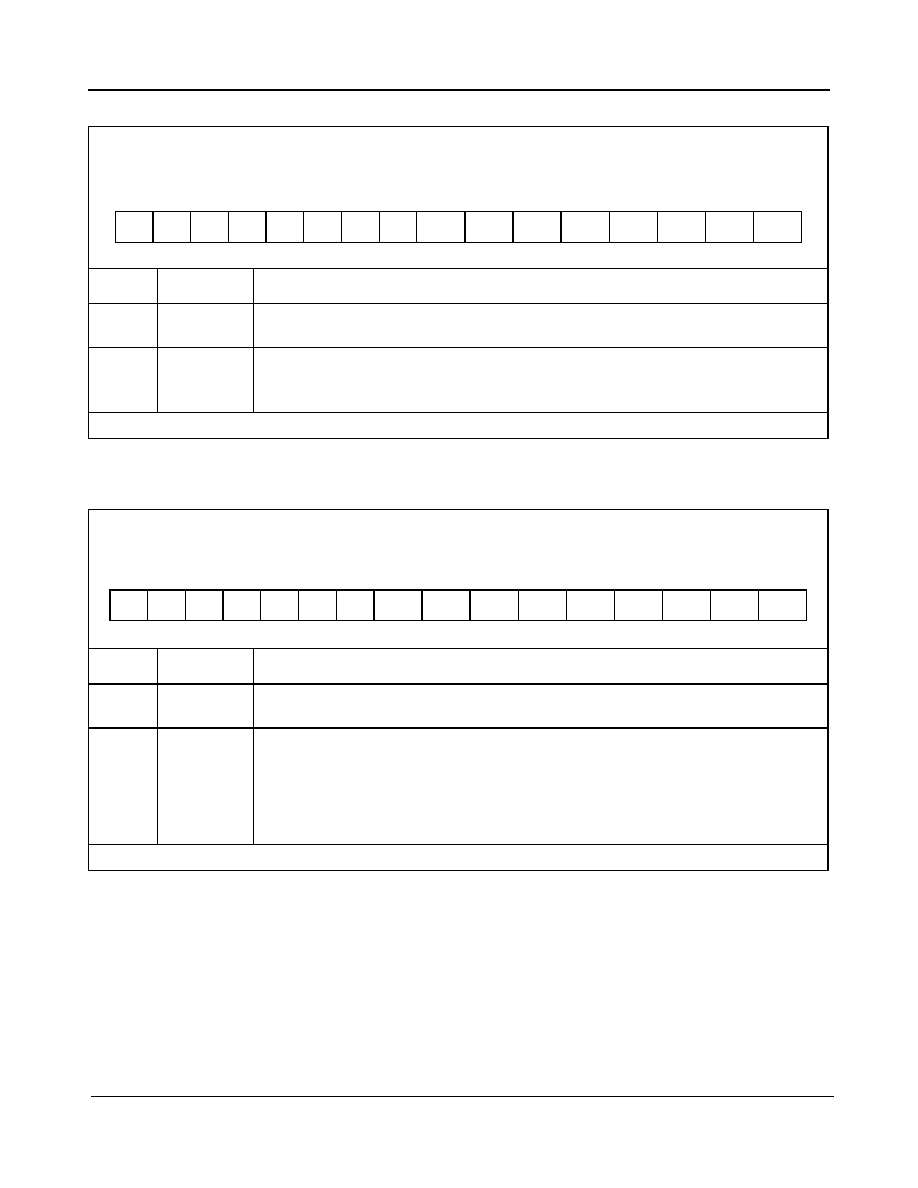
ZL50015
Data Sheet
84
Zarlink Semiconductor Inc.
Bit
Name
Description
15 - 8
Unused
Reserved
In normal functional mode, these bits MUST be set to zero.
7 - 0
ST[n]
BRS7 - 0
Stream[n] BER Receive Start Bits
The binary value of these bits refers to the input channel in which the BER data starts
to be compared.
Note: [n] denotes input stream from 0 - 15
Table 46 - BER Receiver Start Register [n] (BRSR[n]) Bits
Bit
Name
Description
15 - 9
Unused
Reserved
In normal functional mode, these bits MUST be set to zero.
8 - 0
ST[n]
BL8 - 0
Stream[n] BER Length Bits
The binary value of these bits refers to the number of consecutive channels expected
to receive the BER pattern. The maximum number of BER channels is 32, 64, 128 and
256 for the data rates of 2.048 Mbps, 4.096 Mbps, 8.192 Mbps and 16.384 Mbps
respectively. The minimum number of BER channels is 1. If these bits are set to zero,
no BER test will be performed.
Note: [n] denotes input stream from 0 - 15
Table 47 - BER Receiver Length Register [n] (BRLR[n]) Bits
External Read/Write Address: 0300
H
- 030F
H
Reset Value: 0000
H
15
14
13
12
11
10
9
8
7
6
5
4
3
2
1
0
0
0
0
0
0
0
0
0
ST[n]
BRS7
ST[n]
BRS6
ST[n]
BRS5
ST[n]
BRS4
ST[n]
BRS3
ST[n]
BRS2
ST[n]
BRS1
ST[n]
BRS0
External Read/Write Address: 0320
H
- 032F
H
Reset Value: 0000
H
15
14
13
12
11
10
9
8
7
6
5
4
3
2
1
0
0
0
0
0
0
0
0
ST[n]
BL8
ST[n]
BL7
ST[n]
BL6
ST[n]
BL5
ST[n]
BL4
ST[n]
BL3
ST[n]
BL2
ST[n]
BL1
ST[n]
BL0
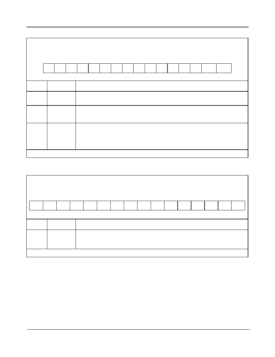
ZL50015
Data Sheet
85
Zarlink Semiconductor Inc.
Bit
Name
Description
15 - 2
Unused
Reserved
In normal functional mode, these bits MUST be set to zero.
1
ST[n]
CBER
Stream[n] Bit Error Rate Counter Clear
When this bit is high, it resets the internal bit error counter and the stream BER
Receiver Error Register to zero.
0
ST[n]
SBER
Stream[n] Bit Error Rate Test Start
When this bit is high, it enables the BER receiver; starts the bit error rate test. The bit
error test result is kept in the BER Receiver Error (BRER[n]) register. Upon the
completion of the BER test, set this bit to zero. Note that the RBEREB bit must be set
in the IMS Register first.
Note: [n] denotes input stream from 0 - 15
Table 48 - BER Receiver Control Register [n] (BRCR[n]) Bits
Bit
Name
Description
15 - 0
ST[n]
BC15 - 0
Stream[n] BER Count Bits (Read Only)
The binary value of these bits refers to the bit error counts. When it reaches its maxi-
mum value of 0xFFFF, the value will be held and will not rollover.
Note: [n] denotes input stream from 0 - 15
Table 49 - BER Receiver Error Register [n] (BRER[n]) Bits - Read Only
External
Read/Write Address: 0340
H
- 034F
H
Reset Value: 0000
H
15
14
13
12
11
10
9
8
7
6
5
4
3
2
1
0
0
0
0
0
0
0
0
0
0
0
0
0
0
0
ST[n]
CBER
ST[n]
SBER
External
Read Address: 0360
H
- 036F
H
Reset Value: 0000
H
15
14
13
12
11
10
9
8
7
6
5
4
3
2
1
0
ST[n]
BC15
ST[n]
BC14
ST[n]
BC13
ST[n]
BC12
ST[n]
BC11
ST[n]
BC10
ST[n]
BC9
ST[n]
BC8
ST[n]
BC7
ST[n]
BC6
ST[n]
BC5
ST[n]
BC4
ST[n]
BC3
ST[n]
BC2
ST[n]
BC1
ST[n]
BC0
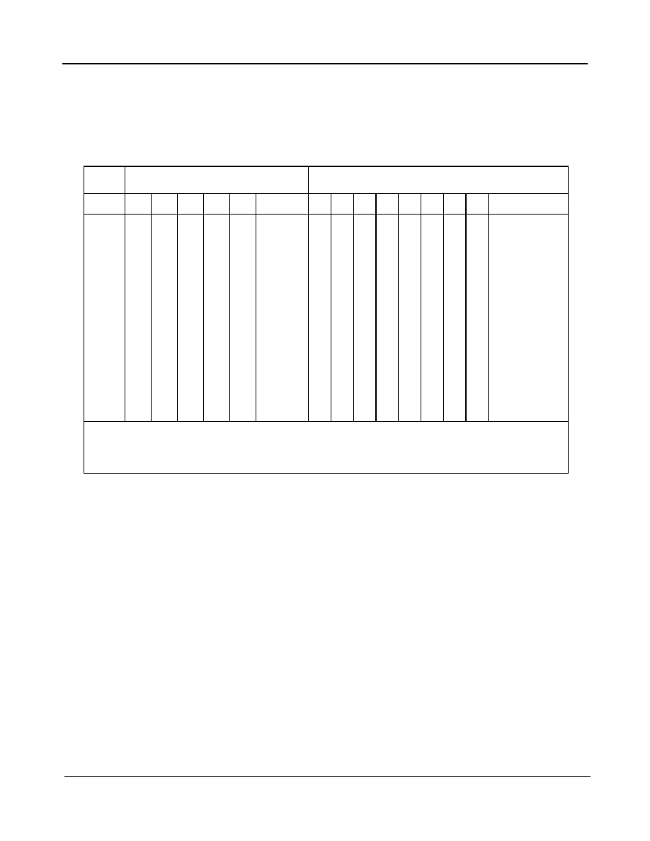
ZL50015
Data Sheet
86
Zarlink Semiconductor Inc.
24.0 Memory
24.1 Memory Address Mappings
When A13 is high, the data or connection memory can be accessed by the microprocessor port. Bit 1 - 0 in the
Control Register determine the access to the data or connection memory (CM_L or CM_H).
MSB
(Note 1)
Stream Address
(St0 - 15)
Channel Address
(Ch0 - 255)
A13
A12
A11
A10
A9
A8
Stream [n]
A7
A6
A5
A4
A3
A2
A1
A0
Channel [n]
1
1
1
1
1
1
1
1
1
.
.
.
.
.
1
1
.
.
0
0
0
0
0
0
0
0
0
.
.
.
.
.
0
0
0
0
0
0
0
0
0
0
1
.
.
.
.
.
1
1
0
0
0
0
1
1
1
1
0
.
.
.
.
.
1
1
0
0
1
1
0
0
1
1
0
.
.
.
.
.
1
1
0
1
0
1
0
1
0
1
0
.
.
.
.
.
0
1
Stream 0
Stream 1
Stream 2
Stream 3
Stream 4
Stream 5
Stream 6
Stream 7
Stream 8
.
.
.
.
.
Stream 14
Stream 15
0
0
.
.
0
0
0
0
.
.
0
0
.
.
.
.
0
0
.
.
.
.
1
1
0
0
.
.
0
0
0
0
.
.
0
0
.
.
.
.
1
1
.
.
.
.
1
1
0
0
.
.
0
0
1
1
.
.
1
1
.
.
.
.
1
1
.
.
.
.
1
1
0
0
.
.
1
1
0
0
1
1
.
.
.
.
1
1
.
.
.
.
1
1
0
0
.
.
1
1
0
0
.
.
1
1
.
.
.
.
1
1
.
.
.
.
1
1
0
0
.
.
1
1
0
0
.
1
1
.
.
.
.
1
1
.
.
.
.
1
1
0
0
.
.
1
1
0
0
1
1
.
.
.
.
1
1
.
.
.
.
1
1
0
1
.
.
0
1
0
1
.
.
0
1
.
.
.
.
0
1
.
.
.
.
0
1
Ch 0
Ch 1
.
.
Ch 30
Ch 31 (Note 2)
Ch 32
Ch 33
.
.
Ch 62
Ch 63 (Note 3)
.
.
.
.
Ch126
Ch 127 (Note 4)
.
.
.
.
Ch 254
Ch 255 (Note 5)
Notes:
1. A13 must be high for access to data and connection memory positions. A13 must be low to access internal registers.
2. Channels 0 to 31 are used when serial stream is at 2.048 Mbps.
3. Channels 0 to 63 are used when serial stream is at 4.096 Mbps.
4. Channels 0 to 127 are used when serial stream is at 8.192 Mbps.
5. Channels 0 to 255 are used when serial stream is at 16.384 Mbps.
Table 50 - Address Map for Memory Locations (A13 = 1)
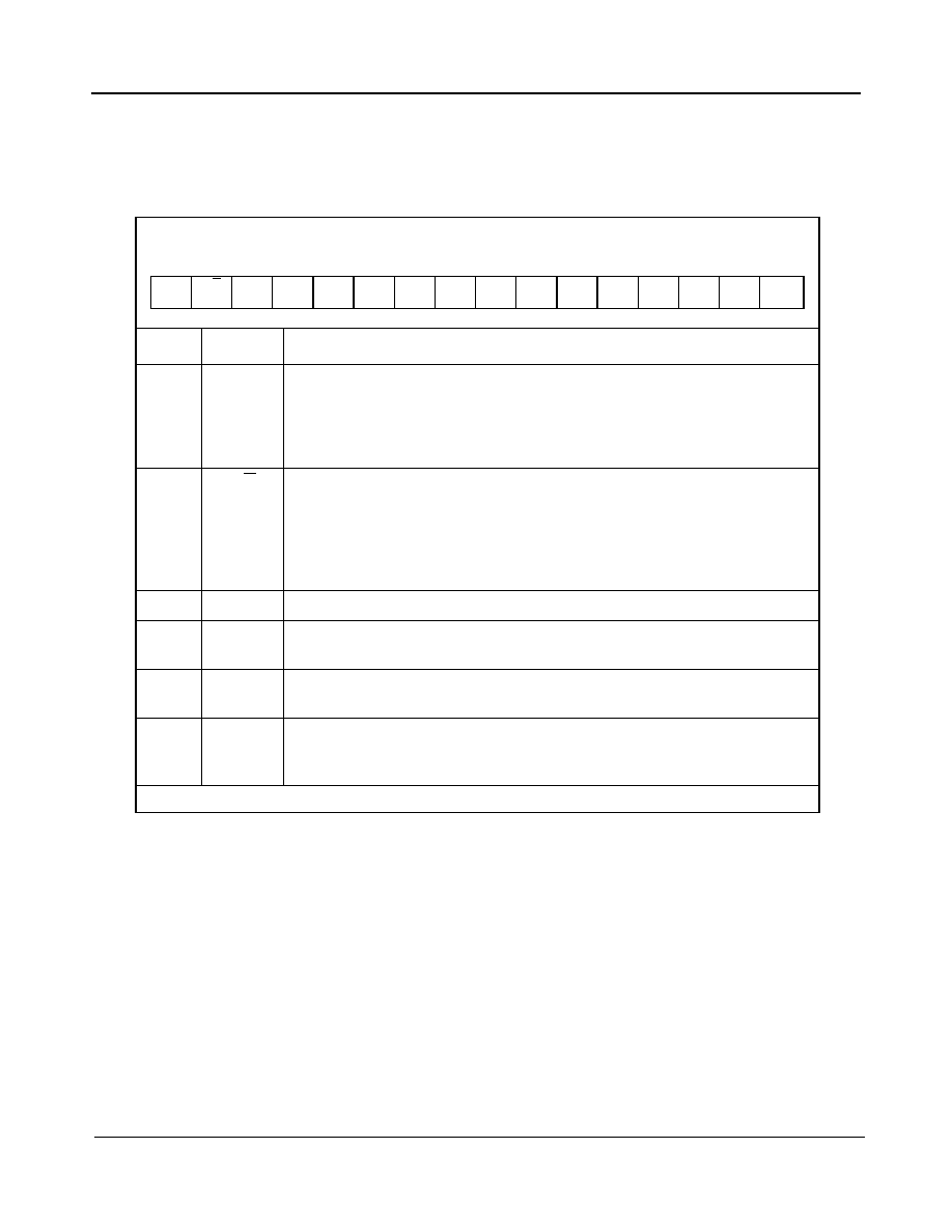
ZL50015
Data Sheet
87
Zarlink Semiconductor Inc.
24.2 Connection Memory Low (CM_L) Bit Assignment
When the CMM bit (bit 0) in the connection memory low is zero, the per-channel transmission is set to the normal
channel-switching. The connection memory low bit assignment for the channel transmission mode is shown in
Table 51 on page 87.
Bit
Name
Description
15
UAEN
Conversion between
µ-law and A-law Enable
When this bit is low, normal switch without
µ-law/A-law conversion. Connec-
tion memory high will be ignored.
When this bit is high, switch with
µ-law/A-law conversion, and connection
memory high controls the conversion method.
14
V/C
Variable/Constant Delay Control
When this bit is low, the output data for this channel will be taken from con-
stant delay memory.
When this bit is set to high, the output data for this channel will be taken from
variable delay memory. Note that VAREN must be set in Control Register
first.
13
Unused
Reserved. In normal functional mode, these bits MUST be set to zero.
12 - 9
SSA3 - 0
Source Stream Address
The binary value of these 4 bits represents the input stream number.
8 - 1
SCA7 - 0
Source Channel Address
The binary value of these 8 bits represents the input channel number.
0
CMM = 0
Connection Memory Mode = 0
If this is low, the connection memory is in the normal switching mode. Bit13 -
1 are the source stream number and channel number.
Note: For proper
µ-
law/A-law conversion, the CM_H bits should be set before Bit 15 (UAEN bit) is set to high.
Table 51 - Connection Memory Low (CM_L) Bit Assignment when CMM = 0
15
14
13
12
11
10
9
8
7
6
5
4
3
2
1
0
UA
EN
V/C
SSA
4
SSA
3
SSA
2
SSA
1
SSA
0
SCA
7
SCA
6
SCA
5
SCA
4
SCA
3
SCA
2
SCA
1
SCA
0
CMM
=0
ZL50015
Data Sheet
88
Zarlink Semiconductor Inc.
When CMM is one, the device is programmed to perform one of the special per-channel transmission modes. Bits
PCC0 and PCC1 from connection memory are used to select the per-channel tristate, message or BER test mode
as shown in Table 52 on page 88.
24.3 Connection Memory High (CM_H) Bit Assignment
Connection memory high provides the detailed information required for
µ-law and A-law conversion. ICL and OCL
bits describe the Input Coding Law and the Output Coding Law, respectively. They are used to select the expected
PCM coding laws for the connection, on the TDM inputs, and on the TDM outputs. The V/D bit is used to select the
class of coding law. If the V/D bit is cleared (to select a voice connection), the ICL and OCL bits select between
A-law and
µ-law specifications related to G.711 voice coding. If the V/D bit is set (to select a data connection), the
ICL and OCL bits select between various bit inverting protocols. These coding laws are illustrated in the following
table. If the ICL is different than the OCL, all data bytes passing through the switch on that particular connection are
translated between the indicated laws. If the ICL and the OCL are the same, no coding law translation is performed.
Bit
Name
Description
15
UAEN
Conversion between
µ-law and A-law Enable (Message mode only)
When this bit is low, message mode has no
µ-law/A-law conversion. Connec-
tion memory high will be ignored.
When this bit is high, message mode has
µ-law/A-law conversion, and con-
nection memory high controls the conversion method.
14 - 11
Unused
Reserved
In normal functional mode, these bits MUST be set to zero.
10 - 3
MSG7 - 0
Message Data Bits
8-bit data for the message mode. Not used in the per-channel tristate and
BER test modes.
2 - 1
PCC1 - 0
Per-Channel Control Bits
These two bits control the corresponding entry's value on the STio stream.
0
CMM = 1
Connection Memory Mode = 1
If this is high, the connection memory is in the per-channel control mode
which is per-channel tristate, per-channel message mode or per-channel BER
mode.
Note: For proper
µ-
law/A-law conversion, the CM_H bits should be set before Bit 15 (UAEN bit) is set to high.
Table 52 - Connection Memory Low (CM_L) Bit Assignment when CMM = 1
15
14
13
12
11
10
9
8
7
6
5
4
3
2
1
0
UA
EN
0
0
0
0
MSG
7
MSG
6
MSG
5
MSG
4
MSG
3
MSG
2
MSG
1
MSG
0
PCC
1
PCC
0
CMM
=1
PC
C1
PC
C0
Channel Output Mode
0
0
Per Channel Tristate
0
1
Message Mode
1
0
BER Test Mode
1
1
Reserved
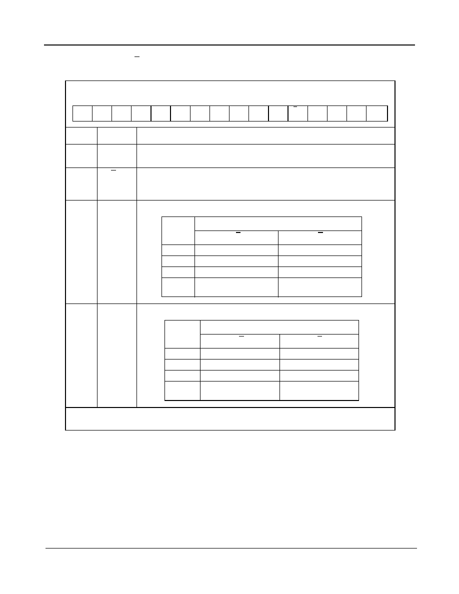
ZL50015
Data Sheet
89
Zarlink Semiconductor Inc.
The ICL, the OCL bits and V/D bit only have an effect on PCM code translations for constant delay connections,
variable delay connections and per-channel message mode.
Bit
Name
Description
15 - 5
Unused
Reserved
In normal functional mode, these bits MUST be set to zero.
4
V/D
Voice/Data Control
When this bit is low, the corresponding channel is for voice.
When this bit is high, the corresponding channel is for data.
3 - 2
ICL1 - 0
Input Coding Law.
1 - 0
OCL1 - 0
Output Coding Law
Note 1: For proper
µ-
law/A-law conversion, the CM_H bits should be set before Bit 15 of CM_L is set to high.
Note 2: Refer to G.711 standard for detail information of different laws.
Table 53 - Connection Memory High (CM_H) Bit Assignment
15
14
13
12
11
10
9
8
7
6
5
4
3
2
1
0
0
0
0
0
0
0
0
0
0
0
0
V/D
ICL
1
ICL
0
OCL
1
OCL
0
ICL1-0
Input Coding Law
For Voice (V/D bit = 0)
For Data (V/D bit = 1)
00
CCITT.ITU A-law
No code
01
CCITT.ITU
µ-law
ABI
10
A-law w/o ABI
Inverted ABI
11
µ-law w/o Magnitude
Inversion
All Bits Inverted
OCL1-0
Output Coding Law
For Voice (V/D bit = 0)
For Data (V/D bit = 1)
00
CCITT.ITU A-law
No code
01
CCITT.ITU
µ-law
ABI
10
A-law w/o ABI
Inverted ABI
11
µ-law w/o Magnitude
Inversion
All Bits Inverted
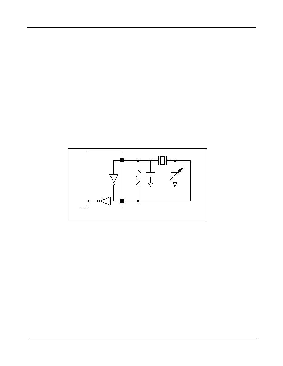
ZL50015
Data Sheet
90
Zarlink Semiconductor Inc.
25.0 Applications
This section contains application-specific details for clock and crystal operation and power supply decoupling.
25.1 OSCi Master Clock Requirement
The device requires a 20 MHz master clock source at the OSCi pin when operating in Master mode or in Divided
Slave with OSC mode. The clock source may be either an external clock oscillator connected to the OSCi pin, or an
external crystal connected between the OSCi and OSCo pins. If an external clock source is present, OSC_EN must
be tied high.
Note that using a crystal is only suitable for wider tolerance applications (e.g.,
±100 ppm). For stratum 4E
applications a clock oscillator with a tolerance of
±32 ppm should be used. See Application Note ZLAN-68 for a list
of Oscillators and Crystals that can be used with Zarlink PLL's and Digital Switches with embedded PLL's.
25.1.1 External Crystal Oscillator
When an external crystal oscillator is used, a complete oscillator circuit made up of a crystal, resistor and capacitors
is shown in Figure 23 on page 90. XC is a buffered version of the 20 MHz input clock connected to the internal
circuitry.
Figure 23 - Crystal Oscillator Circuit
The accuracy of a crystal oscillator circuit depends on the crystal tolerance as well as the load capacitance
tolerance. Typically, for a 20 MHz crystal specified with a 32 pF load capacitance, each 1 pF change in load
capacitance contributes approximately 9 ppm to the frequency deviation. Consequently, capacitor tolerances and
stray capacitances have a major effect on the accuracy of the oscillator frequency. The trimmer capacitor shown in
Figure 23 on page 90 may be used to compensate for capacitive effects.
OSCo
25 pF
1
25 pF
20 MHz
OSCi
XC
1 K DX
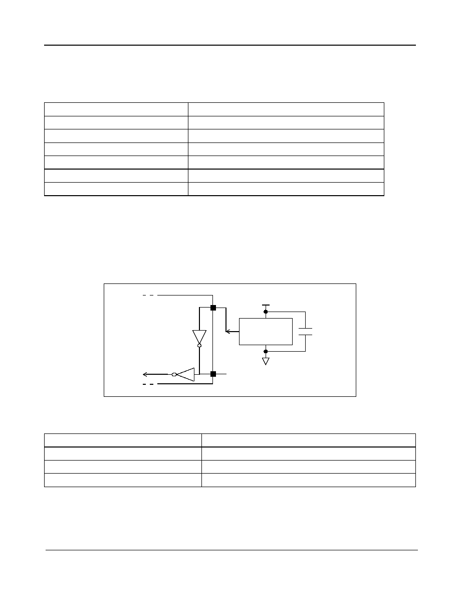
ZL50015
Data Sheet
91
Zarlink Semiconductor Inc.
The crystal should be a fundamental mode type - not an overtone. The fundamental mode crystal permits a simpler
oscillator circuit with no additional filter components and is less likely to generate spurious responses. The crystal
accuracy only affects the output clock accuracy in the freerun or the holdover mode. The crystal specification is as
follows:
25.1.2 External Clock Oscillator
When an external clock oscillator is used, numerous parameters must be considered. They include absolute
frequency, frequency change over temperature, output rise and fall times, output levels and duty cycle.
The output clock should be connected directly (not AC coupled) to the OSCi input of the device, and the OSCo
output should be left open as shown in Figure 24 on page 91. XC is a buffered version of the 20 MHz input clock
connected to the internal circuitry.
Figure 24 - Clock Oscillator Circuit
For applications requiring
±32 ppm clock accuracy, the following requirements should be met.
Frequency
20 MHz
Tolerance As
required
Oscillation Mode
Fundamental
Resonance Mode
Parallel
Load Capacitance
20 pF - 32 pF
Maximum Series Resistance
35
Approximate Drive Level
1 mW
Frequency
20.000 MHz
Tolerance
±32 ppm
Rise and Fall Time
10 ns
Duty Cycle
40% to 60%
+3.3V
20 MHz OUT
GND
0.1 uF
+3.3 V
OSCo
OSCi
No Connection
XC
1K DX
ZL50015
Data Sheet
92
Zarlink Semiconductor Inc.
26.0 DC Parameters
* Exceeding these values may cause permanent damage. Functional operation under these conditions is not implied.
Typical figures are at 25
∞C and are for design aid only: not guaranteed and not subject to production testing.
Characteristics are over recommended operating conditions unless otherwise stated.
Typical figures are at 25
∞C and are for design aid only: not guaranteed and not subject to production testing.
* Note 1: Maximum leakage on pins (output or I/O pins in high impedance state) is over an applied voltage (
V
IN
).
Absolute Maximum Ratings*
Parameter
Symbol
Min.
Max.
Units
1
I/O Supply Voltage
V
DD_IO
-0.5
5.0
V
2
Core Supply Voltage
V
DD_CORE
-0.5
2.5
V
3
Input Voltage
V
I_3V
-0.5
V
DD
+ 0.5
V
4
Input Voltage (5 V-tolerant inputs)
V
I_5V
-0.5
7.0
V
5
Continuous Current at Digital Outputs
I
o
15
mA
6
Package Power Dissipation
P
D
1.5
W
7
Storage Temperature
T
S
- 55
+125
∞C
Recommended Operating Conditions -
Voltages are with respect to ground (V
SS
) unless otherwise stated
.
Characteristics
Sym.
Min.
Typ.
Max.
Units
1
Operating Temperature
T
OP
-40
25
+85
∞C
2
Positive Supply
V
DD_IO
3.0
3.3
3.6
V
3
Positive Supply
V
DD_CORE
1.71
1.8
1.89
V
4
Input Voltage
V
I
0
3.3
V
DD_IO
V
5
Input Voltage on 5 V-Tolerant Inputs
V
I_5V
0
5.0
5.5
V
DC Electrical Characteristics
-
Voltages are with respect to ground (V
ss
) unless otherwise stated.
Characteristics
Sym.
Min.
Typ.
Max.
Units
Test Conditions
1
Supply Current - V
DD_CORE
I
DD_CORE
150
mA
2
Supply Current - V
DD_IO
I
DD_IO
45
mA
C
L
= 30 pF
3
Input High Voltage
V
IH
2.0
V
4
Input Low Voltage
V
IL
0.8
V
5
Input Leakage (input pins)
Input Leakage (bi-directional pins)
I
IL
I
BL
5
5
µA
µA
0
<V
IN
V
DD_IO
See Note 1
6
Weak Pullup Current
I
PU
-33
µA
Input at 0 V
7
Weak Pulldown Current
I
PD
33
µA
Input at V
DD_IO
8
Input Pin Capacitance
C
I
3
pF
9
Output High Voltage
V
OH
2.4
V
I
OH
= 10 mA
10 Output Low Voltage
V
OL
0.4
V
I
OL
= 10 mA
11 Output High Impedance Leakage
I
OZ
5
µA
0 < V < V
DD
12 Output Pin Capacitance
C
O
5
10
pF
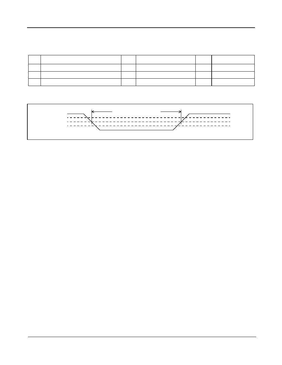
ZL50015
Data Sheet
93
Zarlink Semiconductor Inc.
27.0 AC Parameters
Characteristics are over recommended operating conditions unless otherwise stated.
Figure 25 - Timing Parameter Measurement Voltage Levels
AC Electrical Characteristics
- Timing Parameter Measurement Voltage Levels
Characteristics
Sym.
Level
Units
Conditions
1
CMOS Threshold
V
CT
0.5 V
DD_IO
V
2
Rise/Fall Threshold Voltage High
V
HM
0.7 V
DD_IO
V
3
Rise/Fall Threshold Voltage Low
V
LM
0.3 V
DD_IO
V
Timing Reference Points
ALL SIGNALS
V
HM
V
CT
V
LM
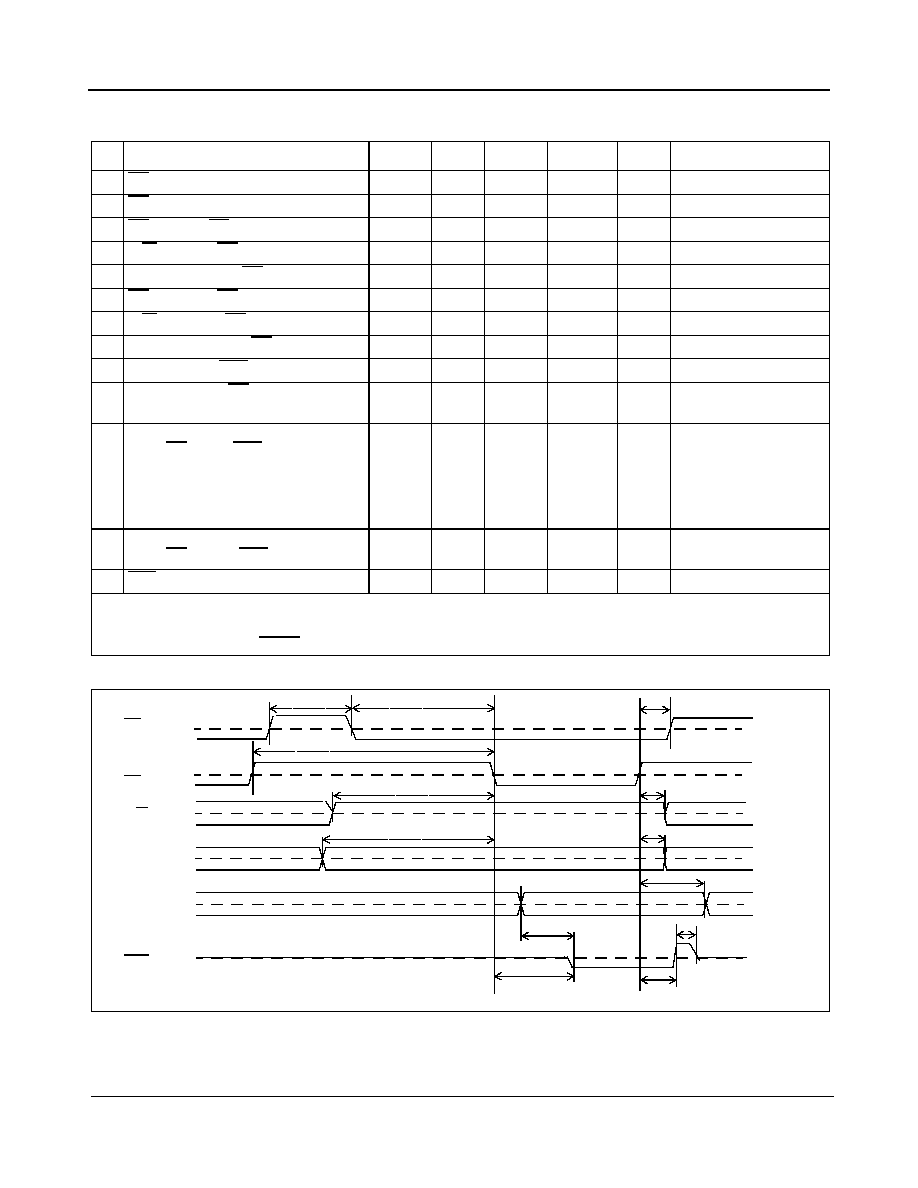
ZL50015
Data Sheet
94
Zarlink Semiconductor Inc.
Characteristics are over recommended operating conditions unless otherwise stated.
Figure 26 - Motorola Non-Multiplexed Bus Timing - Read Access
AC Electrical Characteristics
- Motorola Non-Multiplexed Bus Mode - Read Access
Characteristics
Sym
Min.
Typ.
Max.
Units
Test Conditions
2
1 CS de-asserted time
t
CSD
15
ns
2 DS de-asserted time
t
DSD
15
ns
3 CS setup to DS falling
t
CSS
0
ns
4 R/W setup to DS falling
t
RWS
10
ns
5 Address setup to DS falling
t
AS
5
ns
6 CS hold after DS rising
t
CSH
0
ns
7 R/W hold after DS rising
t
RWH
0
ns
8 Address hold after DS rising
t
AH
0
ns
9 Data setup to DTA Low
t
DS
8
ns
C
L
= 50 pF
10 Data hold after DS rising
t
DH
7
ns
C
L
= 50 pF, R
L
= 1 K
(Note 1)
11 Acknowledgement delay time.
From DS low to DTA low:
Registers
Memory
t
AKD
75
185
ns
ns
C
L
= 50 pF
C
L
= 50 pF
12 Acknowledgement hold time.
From DS high to DTA high
t
AKH
4
12
ns
C
L
= 50 pF, R
L
= 1 K
(Note 1)
13 DTA drive high to HiZ
t
AKZ
8
ns
Note 1: High impedance is measured by pulling to the appropriate rail with R
L
, with timing corrected to cancel time taken to
discharge C
L
.
Note 2: A delay of 500
µs to 2 ms (see Section 17.2 on page 46) must be applied before the first microprocessor access is
performed after the RESET pin is set high.
DS
A0-A13
D0-D15
t
CSH
t
AH
t
RWS
R/W
t
AS
t
RWH
t
AKD
t
DS
t
AKH
DTA
V
CT
V
CT
V
CT
V
CT
V
CT
V
CT
VALID ADDRESS
VALID READ DATA
t
CSS
t
DSD
CS
t
AKZ
t
CSD
t
DH
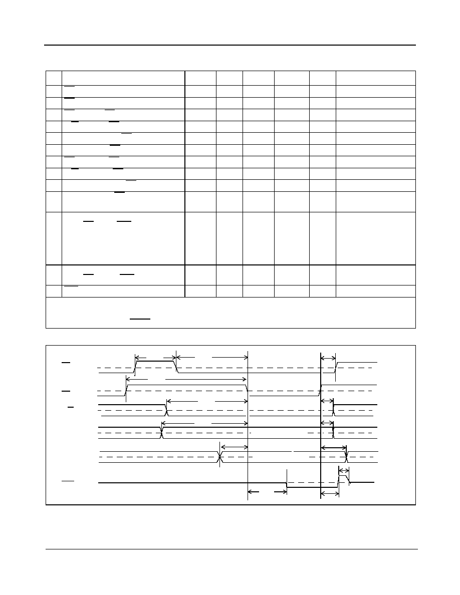
ZL50015
Data Sheet
95
Zarlink Semiconductor Inc.
Characteristics are over recommended operating conditions unless otherwise stated.
Figure 27 - Motorola Non-Multiplexed Bus Timing - Write Access
AC Electrical Characteristics
- Motorola Non-Multiplexed Bus Mode - Write Access
Characteristics
Sym.
Min.
Typ.
Max.
Units
Test Conditions
2
1 CS de-asserted time
t
CSD
15
ns
2 DS de-asserted time
t
DSD
15
ns
3 CS setup to DS falling
t
CSS
0
ns
4 R/W setup to DS falling
t
RWS
10
ns
5 Address setup to DS falling
t
AS
5
ns
6 Data setup to DS falling
t
DS
0
ns
C
L
= 50 pF
7 CS hold after DS rising
t
CSH
0
ns
8 R/W hold after DS rising
t
RWH
0
ns
9 Address hold after DS rising
t
AH
0
ns
10 Data hold from DS rising
t
DH
5
ns
C
L
= 50 pF, R
L
= 1 K
(Note 1)
11 Acknowledgement delay time.
From DS low to DTA low:
Registers
Memory
t
AKD
55
150
ns
ns
C
L
= 50 pF
C
L
= 50 pF
12 Acknowledgement hold time.
From DS high to DTA high
t
AKH
4
12
ns
C
L
= 50 pF, R
L
= 1 K
(Note 1)
13 DTA drive high to HiZ
t
AKZ
8
ns
Note 1: High impedance is measured by pulling to the appropriate rail with R
L
, with timing corrected to cancel time taken to
discharge C
L
.
Note 2: A delay of 500
µs to 2 ms (see Section 17.2 on page 46) must be applied before the first microprocessor access is
performed after the RESET pin is set high.
DS
A0-A13
t
CSH
t
AH
t
RWS
R/W
t
AS
t
RWH
t
AKD
t
AKH
DTA
V
CT
V
CT
V
CT
V
CT
V
CT
t
CSS
t
DSD
CS
t
AKZ
D0-D15
t
DH
t
DS
V
CT
VALID WRITE DATA
t
CSD
VALID ADDRESS
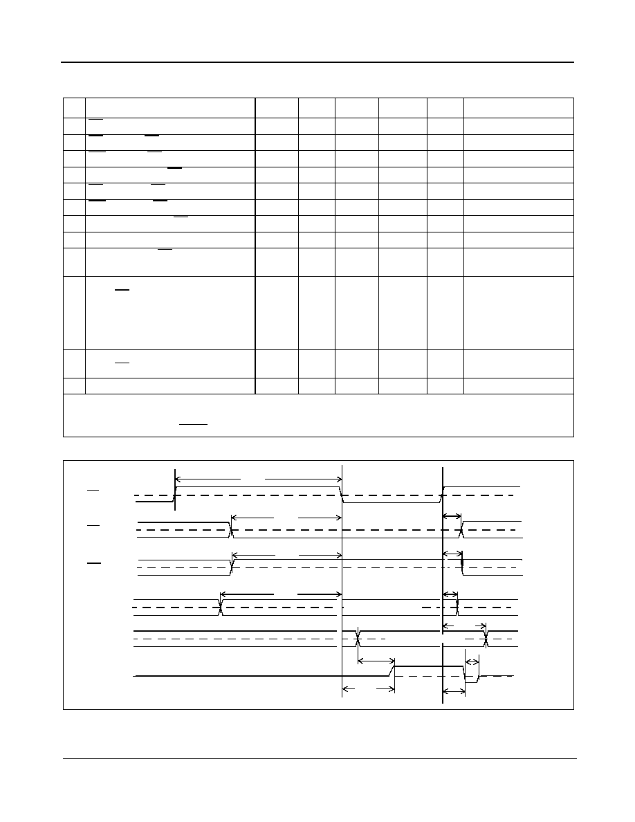
ZL50015
Data Sheet
96
Zarlink Semiconductor Inc.
Characteristics are over recommended operating conditions unless otherwise stated.
Figure 28 - Intel Non-Multiplexed Bus Timing - Read Access
AC Electrical Characteristics
- Intel Non-Multiplexed Bus Mode - Read Access
Characteristics
Sym.
Min.
Typ.
Max.
Units
Test Conditions
2
1 CS de-asserted time
t
CSD
15
ns
2 RD setup to CS falling
t
RS
10
ns
3 WR setup to CS falling
t
WS
10
ns
4 Address setup to CS falling
t
AS
5
ns
5 RD hold after CS rising
t
RH
0
ns
6 WR hold after CS rising
t
WH
0
ns
7 Address hold after CS rising
t
AH
0
ns
8 Data setup to RDY high
t
DS
8
ns
C
L
= 50 pF
9 Data hold after CS rising
t
DH
7
ns
C
L
= 50 pF, R
L
= 1 K
(Note 1)
10 Acknowledgement delay time.
From CS low to RDY high:
Registers
Memory
t
AKD
75
185
ns
ns
C
L
= 50 pF
C
L
= 50 pF
11 Acknowledgement hold time.
From CS high to RDY low
t
AKH
4
12
ns
C
L
= 50 pF, R
L
= 1 K
(Note 1)
12 RDY drive low to HiZ
t
AKZ
8
ns
Note 1: High impedance is measured by pulling to the appropriate rail with R
L
, with timing corrected to cancel time taken to
discharge C
L
.
Note 2: A delay of 500
µs to 2 ms (see Section 17.2 on page 46) must be applied before the first microprocessor access is
performed after the RESET pin is set high.
CS
A0-A13
D0-D15
t
AH
t
WS
WR
t
WH
t
AKD
t
DS
t
AKH
RDY
V
CT
V
CT
V
CT
V
CT
V
CT
VALID ADDRESS
VALID READ DATA
t
CSD
t
AKZ
t
RS
RD
t
RH
V
CT
t
AS
t
DH
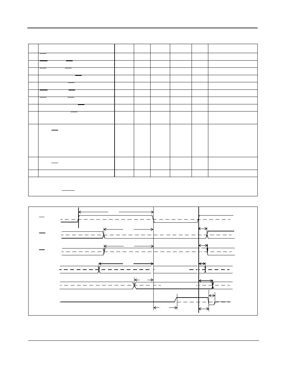
ZL50015
Data Sheet
97
Zarlink Semiconductor Inc.
Characteristics are over recommended operating conditions unless otherwise stated.
Figure 29 - Intel Non-Multiplexed Bus Timing - Write Access
AC Electrical Characteristics
- Intel Non-Multiplexed Bus Mode - Write Access
Characteristics
Sym.
Min.
Typ.
Max.
Units
Test Conditions
2
1 CS de-asserted time
t
CSD
15
ns
2 WR setup to CS falling
t
WS
10
ns
3 RD setup to CS falling
t
RS
10
ns
4 Address setup to CS falling
t
AS
5
ns
5 Data setup to CS falling
t
DS
0
ns
C
L
= 50 pF
6 WR hold after CS rising
t
WH
0
ns
7 RD hold after CS rising
t
RH
0
ns
8 Address hold after CS rising
t
AH
10
ns
9 Data hold after CS rising
t
DH
5
ns
C
L
= 50 pF, R
L
= 1 K
(Note 1)
10 Acknowledgement delay time.
From CS low to RDY high:
Registers
Memory
t
AKD
55
150
ns
ns
C
L
= 50 pF
C
L
= 50 pF
11 Acknowledgement hold time.
From CS high to RDY low
t
AKH
4
12
ns
C
L
= 50 pF, R
L
= 1 K
(Note 1)
12 RDY drive low to HiZ
t
AKZ
8
ns
Note 1: High impedance is measured by pulling to the appropriate rail with R
L
, with timing corrected to cancel time taken to
discharge C
L
.
Note 2: A delay of 500
µs to 2 ms (Section 17.2 on page 46) must be applied before the first microprocessor access is performed
after the RESET pin is set high.
CS
A0-A13
D0-D15
t
AH
t
RS
RD
t
RH
t
AKD
t
AKH
RDY
V
CT
V
CT
V
CT
V
CT
V
CT
VALID ADDRESS
t
CSD
t
AKZ
t
WS
WR
t
WH
V
CT
t
AS
VALID WRITE DATA
t
DS
t
DH
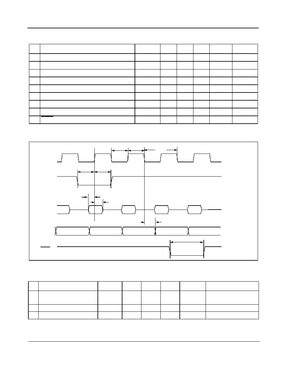
ZL50015
Data Sheet
98
Zarlink Semiconductor Inc.
Characteristics are over recommended operating conditions unless otherwise stated.
Figure 30 - JTAG Test Port Timing Diagram
Characteristics are over recommended operating conditions unless otherwise stated.
See "Performance Characteristics Notes" on page 119.
AC Electrical Characteristics
- JTAG Test Port Timing
Characteristic
Sym.
Min.
Typ.
Max.
Units
Notes
1
TCK Clock Period
t
TCKP
100
ns
2
TCK Clock Pulse Width High
t
TCKH
20
ns
3
TCK Clock Pulse Width Low
t
TCKL
20
ns
4
TMS Set-up Time
t
TMSS
10
ns
5
TMS Hold Time
t
TMSH
10
ns
6
TDi Input Set-up Time
t
TDIS
20
ns
7
TDi Input Hold Time
t
TDIH
60
ns
8
TDo Output Delay
t
TDOD
30
ns
C
L
= 30 pF
9
TRST pulse width
t
TRSTW
200
ns
AC Electrical Characteristics
- OSCi 20 MHz Input Timing
Characteristic
Sym.
Min.
Typ.
Max.
Units
Notes
1
Input frequency accuracy
-32
-100
32
100
ppm
ppm
Stratum 4E
Relaxed Stratum 4E
2
Duty cycle
40
60
%
1
3
Input rise or fall time
t
IR,
t
IF
3
ns
14
t
TMSH
t
TMSS
t
TCKL
t
TCKH
t
TCKP
t
TDIS
t
TDIH
t
TDOD
t
TRSTW
TMS
TCK
TDi
TDo
TRST
ZL50015
Data Sheet
99
Zarlink Semiconductor Inc.
Characteristics are over recommended operating conditions unless otherwise stated.
Typical figures are at 25
∞C and are for design aid only: not guaranteed and not subject to production testing.
Characteristics are over recommended operating conditions unless otherwise stated.
Typical figures are at 25
∞C and are for design aid only: not guaranteed and not subject to production testing.
Characteristics are over recommended operating conditions unless otherwise stated.
Typical figures are at 25
∞C and are for design aid only: not guaranteed and not subject to production testing.
AC Electrical Characteristics
- FPi and CKi Timing when CKIN1-0 bits = 00 (16.384 MHz)
Characteristic
Sym.
Min.
Typ.
Max. Units Notes
1
FPi Input Frame Pulse Width
t
FPIW
40
61
115
ns
2
FPi Input Frame Pulse Setup Time
t
FPIS
20
ns
3
FPi Input Frame Pulse Hold Time
t
FPIH
20
ns
4
CKi Input Clock Period
t
CKIP
55
61
67
ns
5
CKi Input Clock High Time
t
CKIH
27
34
ns
6
CKi Input Clock Low Time
t
CKIL
27
34
ns
7
CKi Input Clock Rise/Fall Time
t
r
CKi, t
f
CKi
3
ns
8
CKi Input Clock Cycle to Cycle Variation
t
CVC
0
20
ns
AC Electrical Characteristics
- FPi and CKi Timing when CKIN1-0 bits = 01 (8.192 MHz)
Characteristic
Sym.
Min.
Typ.
Max. Units Notes
1
FPi Input Frame Pulse Width
t
FPIW
90
122
220
ns
2
FPi Input Frame Pulse Setup Time
t
FPIS
45
ns
3
FPi Input Frame Pulse Hold Time
t
FPIH
45
ns
4
CKi Input Clock Period
t
CKIP
110
122
135
ns
5
CKi Input Clock High Time
t
CKIH
55
69
ns
6
CKi Input Clock Low Time
t
CKIL
55
69
ns
7
CKi Input Clock Rise/Fall Time
t
r
CKi, t
f
CKi
3
ns
8
CKi Input Clock Cycle to Cycle Variation
t
CVC
0
20
ns
AC Electrical Characteristics
- FPi and CKi Timing when CKIN1-0 bits = 10 (4.096 MHz)
Characteristic
Sym.
Min.
Typ.
Max. Units Notes
1
FPi Input Frame Pulse Width
t
FPIW
90
244
420
ns
2
FPi Input Frame Pulse Setup Time
t
FPIS
110
ns
3
FPi Input Frame Pulse Hold Time
t
FPIH
110
ns
4
CKi Input Clock Period
t
CKIP
220
244
270
ns
5
CKi Input Clock High Time
t
CKIH
110
135
ns
6
CKi Input Clock Low Time
t
CKIL
110
135
ns
7
CKi Input Clock Rise/Fall Time
t
r
CKi, t
f
CKi
3
ns
8
CKi Input Clock Cycle to Cycle Variation
t
CVC
0
20
ns

ZL50015
Data Sheet
100
Zarlink Semiconductor Inc.
Figure 31 - Frame Pulse Input and Clock Input Timing Diagram (ST-BUS)
Figure 32 - Frame Pulse Input and Clock Input Timing Diagram (GCI-Bus)
t
FPIW
FPi
t
FPIH
t
CKIH
t
CKIL
t
FPIS
t
CKIP
CKi
Input Frame Boundary
t
rCKI
t
fCKI
t
FPIW
FPi
t
FPIH
t
CKIH
t
CKIL
t
FPIS
t
CKIP
CKi
Input Frame Boundary
t
rCKI
t
fCKI
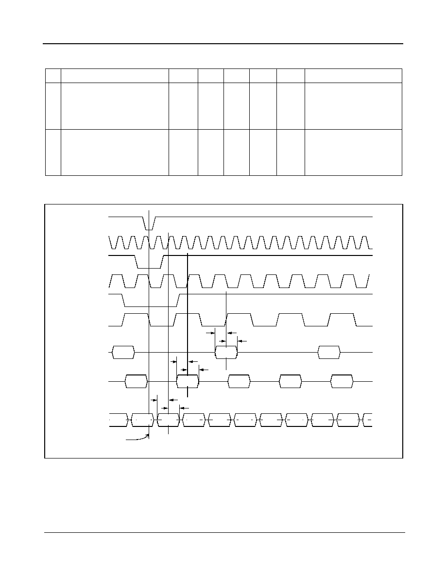
ZL50015
Data Sheet
101
Zarlink Semiconductor Inc.
Characteristics are over recommended operating conditions unless otherwise stated.
Figure 33 - ST-BUS Input Timing Diagram when Operated at 2 Mbps, 4 Mbps, 8 Mbps
AC Electrical Characteristics
- ST-BUS/GCI-Bus Input Timing
Characteristic
Sym.
Min.
Typ.
Max.
Units
Test Conditions
1 STi Setup Time
2.048 Mbps
4.096 Mbps
8.192 Mbps
16.384 Mbps
t
SIS2
t
SIS4
t
SIS8
t
SIS16
5
5
5
ns
ns
ns
ns
2 STi Hold Time
2.048 Mbps
4.096 Mbps
8.192 Mbps
16.384 Mbps
t
SIH2
t
SIH4
t
SIH8
t
SIH16
8
8
8
ns
ns
ns
ns
V
TT
CKi
FPi
(16.384 MHz)
CKi
FPi
(8.192 MHz)
CKi
FPi
(4.096 MHz)
t
SIS2
t
SIH2
Bit7
Ch0
Bit6
Ch0
t
SIS4
t
SIH4
Bit7
Ch0
Bit6
Ch0
Bit5
Ch0
Bit4
Ch0
Bit0
Ch63
Bit7
Ch0
Bit6
Ch0
Bit5
Ch0
Bit4
Ch0
Bit3
Ch0
Bit2
Ch0
Bit1
Ch0
Bit0
Ch0
Bit1
Ch127
8.192 Mbps
4.096 Mbps
2.048 Mbps
t
SIS8
t
SIH8
STi0 - 15
STi0 - 15
STi0 - 15
V
CT
V
CT
Bit0
Ch31
V
CT
Input Frame Boundary
Bit0
Ch127
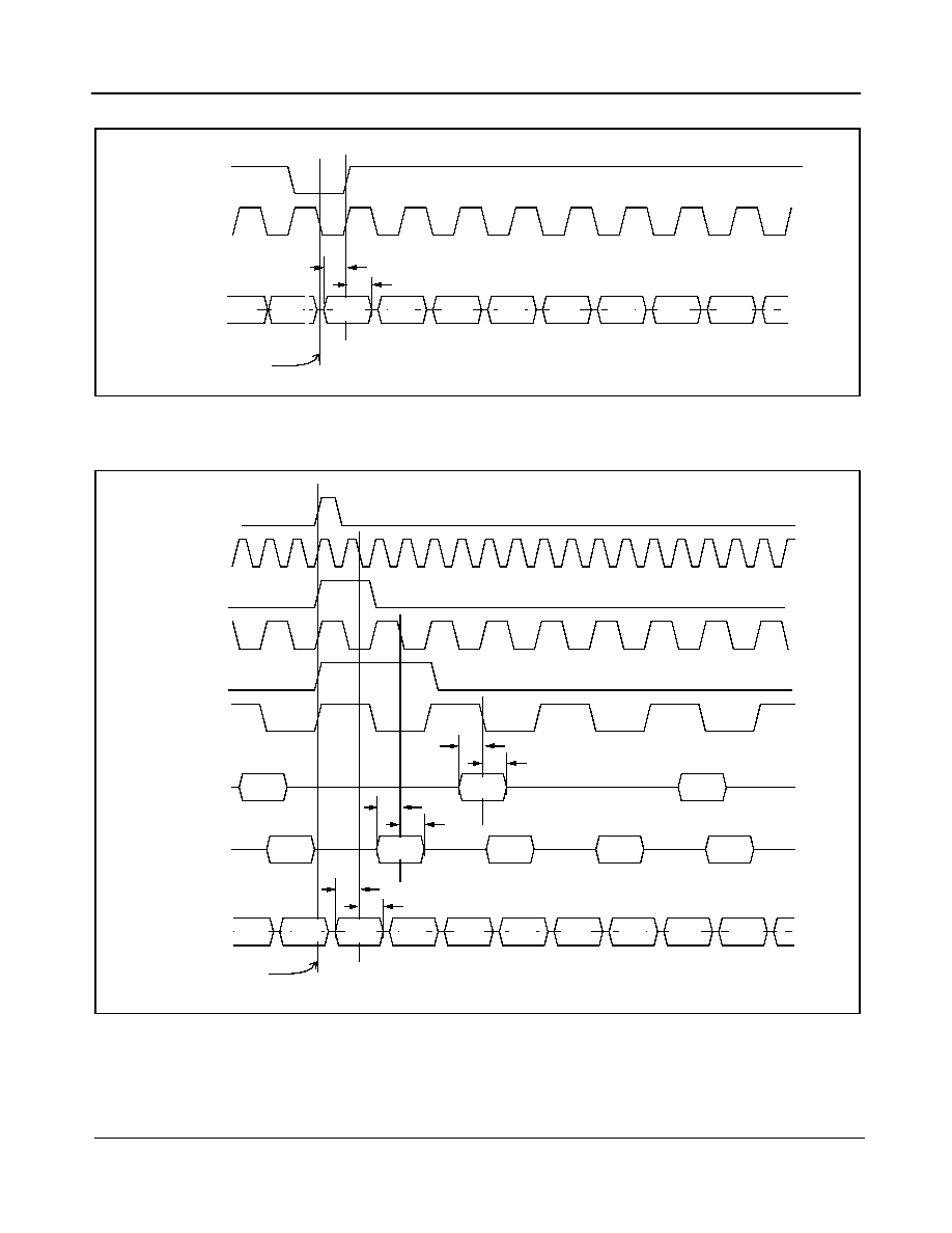
ZL50015
Data Sheet
102
Zarlink Semiconductor Inc.
Figure 34 - ST-BUS Input Timing Diagram when Operated at 16 Mbps
Figure 35 - GCI-Bus Input Timing Diagram when Operated at 2 Mbps, 4 Mbps, 8 Mbps
V
TT
CKi
FPi
(16.384 MHz)
Bit0
Ch255
Bit6
Ch0
Bit5
Ch0
Bit4
Ch0
Bit3
Ch0
Bit2
Ch0
Bit1
Ch0
Bit0
Ch0
Bit1
Ch255
16.384 Mbps
t
SIS16
t
SIH16
Input Frame Boundary
STi0 - 15
V
CT
Bit7
Ch0
V
TT
CKi
FPi
(16.384 MHz)
CKi
FPi
(8.192 MHz)
CKi
FPi
(4.096 MHz)
t
SIS2
t
SIH2
Bit0
Ch0
Bit1
Ch0
t
SIS4
t
SIH4
Bit0
Ch0
Bit1
Ch0
Bit2
Ch0
Bit3
Ch0
Bit7
Ch63
Bit0
Ch0
Bit1
Ch0
Bit2
Ch0
Bit3
Ch0
Bit4
Ch0
Bit5
Ch0
Bit6
Ch0
Bit7
Ch0
Bit6
Ch127
8.192 Mbps
4.096 Mbps
2.048 Mbps
t
SIS8
t
SIH8
STi0 - 15
STi0 - 15
STi0 - 15
V
CT
V
CT
Bit7
Ch31
V
CT
Input Frame Boundary
Bit7
Ch127
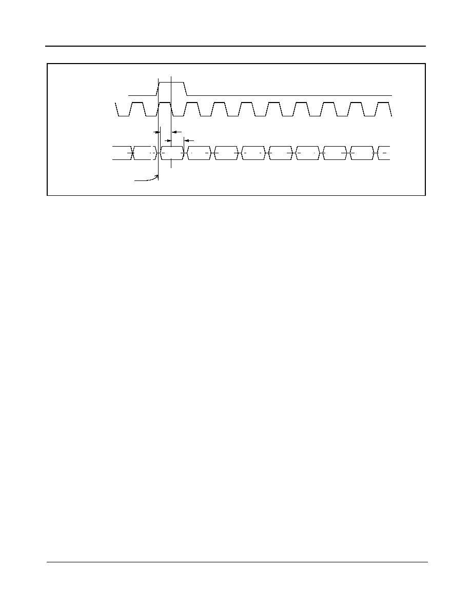
ZL50015
Data Sheet
103
Zarlink Semiconductor Inc.
Figure 36 - GCI-Bus Input Timing Diagram when Operated at 16 Mbps
V
TT
CKi
FPi
(16.384 MHz)
Bit7
Ch255
Bit1
Ch0
Bit2
Ch0
Bit3
Ch0
Bit4
Ch0
Bit5
Ch0
Bit6
Ch0
Bit7
Ch0
Bit6
Ch255
16.384 Mbps
t
SIS16
t
SIH16
Input Frame Boundary
STi0 - 15
V
CT
Bit0
Ch0
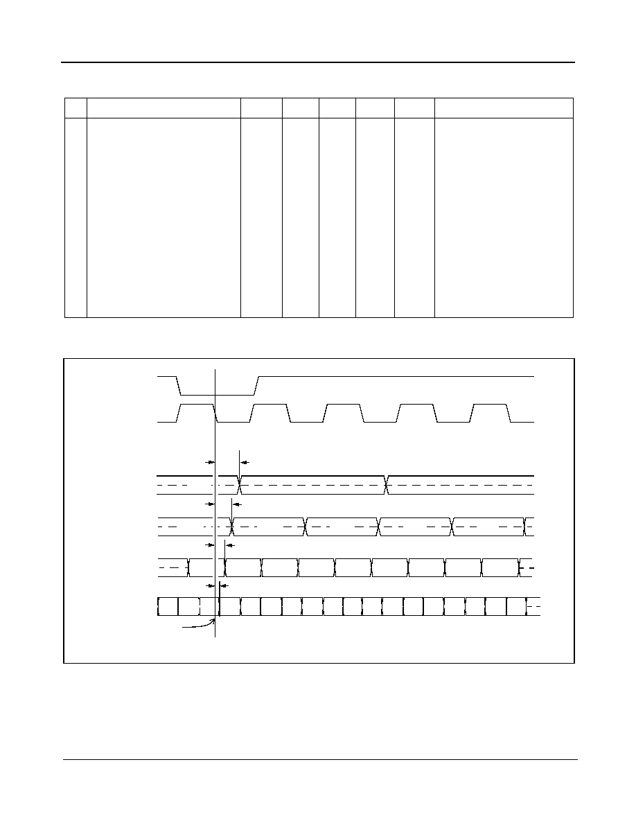
ZL50015
Data Sheet
104
Zarlink Semiconductor Inc.
Characteristics are over recommended operating conditions unless otherwise stated.
Figure 37 - ST-BUS Output Timing Diagram when Operated at 2, 4, 8 or 16 Mbps
AC Electrical Characteristics
- ST-BUS/GCI-Bus Output Timing
Characteristic
Sym.
Min.
Typ.
Max.
Units
Test Conditions
1 STio Delay - Active to Active
@2.048 Mbps
@4.096 Mbps
@8.192 Mbps
@16.384 Mbps
@2.048 Mbps
@4.096 Mbps
@8.192 Mbps
@16.384 Mbps
@2.048 Mbps
@4.096 Mbps
@8.192 Mbps
@16.384 Mbps
t
SOD2
t
SOD4
t
SOD8
t
SOD16
t
SOD2
t
SOD4
t
SOD8
t
SOD16
t
SOD2
t
SOD4
t
SOD8
t
SOD16
1
1
1
1
0
0
0
0
-6
-6
-6
-6
8
8
8
8
6
6
6
6
0
0
0
0
ns
ns
ns
ns
ns
ns
ns
ns
ns
ns
ns
ns
C
L
= 30 pF
Master Mode
Multiplied Slave Mode
Divided Slave Mode
Bit0
Ch255
CKo0
FPo0
(4.096 MHz)
8.192 Mbps
4.096 Mbps
2.048 Mbps
Output Frame Boundary
STio0 - 15
STio0 - 15
STio0 - 15
Bit7
Ch0
Bit6
Ch0
Bit5
Ch0
Bit4
Ch0
Bit0
Ch63
Bit7
Ch0
Bit6
Ch0
Bit0
Ch31
t
SOD2
t
SOD4
t
SOD8
V
CT
V
CT
V
CT
Bit0
Ch127
Bit7
Ch0
Bit6
Ch0
Bit5
Ch0
Bit4
Ch0
Bit3
Ch0
Bit2
Ch0
Bit1
Ch0
Bit0
Ch0
Bit7
Ch0
Bit6
Ch0
Bit5
Ch0
Bit4
Ch0
Bit3
Ch0
Bit2
Ch255
Bit1
Ch255
Bit2
Ch0
Bit1
Ch0
Bit0
Ch0
Bit7
Ch1
Bit6
Ch1
Bit5
Ch1
Bit4
Ch1
Bit3
Ch1
Bit2
Ch1
Bit1
Ch1
V
CT
t
SOD16
16.384 Mbps
STio0 - 15

ZL50015
Data Sheet
105
Zarlink Semiconductor Inc.
Figure 38 - GCI-Bus Output Timing Diagram when Operated at 2, 4, 8 or 16 Mbps
CKo0
FPo0
(4.096 MHz)
Output Frame Boundary
Bit7
Ch255
8.192 Mbps
4.096 Mbps
2.048 Mbps
STio0 - 15
STio0 - 15
STio0 - 15
Bit0
Ch0
Bit1
Ch0
Bit2
Ch0
Bit3
Ch0
Bit7
Ch63
Bit0
Ch0
Bit1
Ch0
Bit7
Ch31
t
SOD2
t
SOD4
t
SOD8
V
CT
V
CT
V
CT
Bit7
Ch127
Bit0
Ch0
Bit1
Ch0
Bit2
Ch0
Bit3
Ch0
Bit4
Ch0
Bit5
Ch0
Bit6
Ch0
Bit7
Ch0
Bit0
Ch0
Bit1
Ch0
Bit2
Ch0
Bit3
Ch0
Bit4
Ch0
Bit5
Ch255
Bit6
Ch255
Bit5
Ch0
Bit6
Ch0
Bit7
Ch0
Bit0
Ch1
Bit1
Ch1
Bit2
Ch1
Bit3
Ch1
Bit4
Ch1
Bit5
Ch1
Bit6
Ch1
V
CT
t
SOD16
16.384 Mbps
STio0 - 15
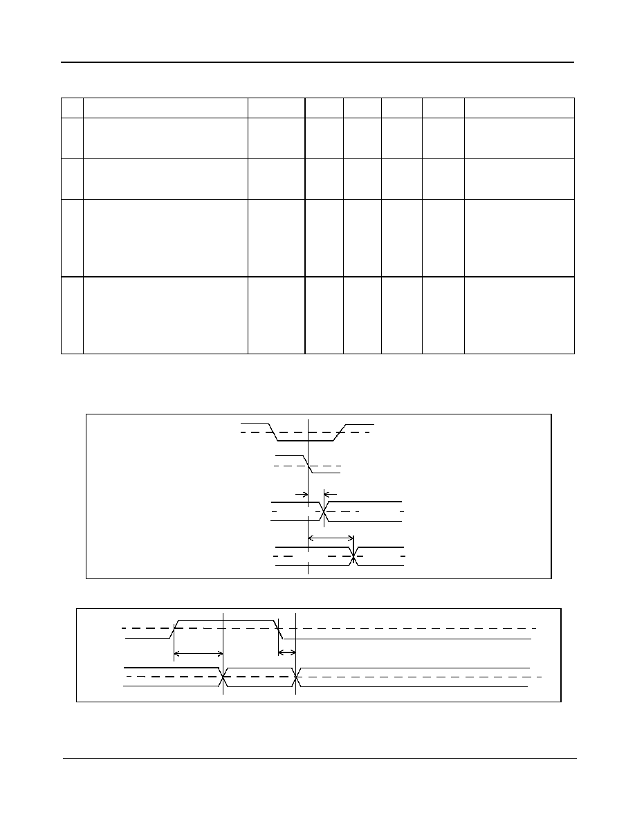
ZL50015
Data Sheet
106
Zarlink Semiconductor Inc.
Characteristics are over recommended operating conditions unless otherwise stated.
* Test condition is R
L
= 1 k, C
L
= 30 pF; high impedance is measured by pulling to the appropriate rail with R
L
, with timing corrected to cancel
the time taken to discharge C
L
.
Figure 39 - Serial Output and External Control
Figure 40 - Output Drive Enable (ODE)
AC Electrical Characteristics
- ST-BUS/GCI-Bus Output Tristate Timing
Characteristic
Sym.
Min.
Typ.
Max.
Units
Test Conditions
*
1 STio Delay - Active to High-Z
t
DZ
-2
-3
-8
8
7
0
ns
ns
ns
Master Mode
Multiplied Slave Mode
Divided Slave Mode
2 STio Delay - High-Z to Active
t
ZD
-2
-3
-8
8
7
0
ns
ns
ns
Master Mode
Multiplied Slave Mode
Divided Slave Mode
3 Output Drive Enable (ODE) Delay
- High-Z to Active
CKi @ 4.096 MHz
CKi @ 8.192 MHz
CKi @ 16.384 MHz
t
ZD_ODE
77
260
138
77
ns
ns
ns
ns
Master or
Multiplied Slave Mode
Divided Slave Mode
4 Output Drive Enable (ODE) Delay
- Active to High-Z
CKi @ 4.096 MHz
CKi @ 8.192 MHz
CKi @ 16.384 MHz
t
DZ_ODE
77
260
138
77
ns
ns
ns
Master or
Multiplied Slave Mode
Divided Slave Mode
t
DZ
STio
t
ZD
STio
CKo0
V
CT
V
CT
Tristate
Valid Data
V
CT
Tristate
Valid Data
FPo0
V
CT
HiZ
HiZ
STio
ODE
t
ZD_ODE
Valid Data
t
DZ_ODE
V
CT
V
CT
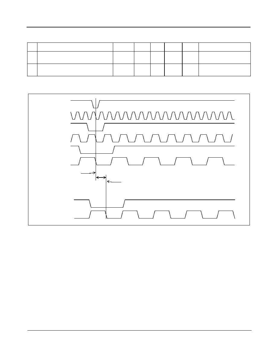
ZL50015
Data Sheet
107
Zarlink Semiconductor Inc.
Characteristics are over recommended operating conditions unless otherwise stated.
Figure 41 - Input and Output Frame Boundary Offset
AC Electrical Characteristics
- Slave Mode Input/Output Frame Boundary Alignment
Characteristic
Sym.
Min.
Typ.
Max.
Units
Notes
1
Input and Output Frame Offset in
Divided Slave Mode
tFBOS
5
13
ns
2
Input and Output Frame Offset in
Multiplied Slave Mode
tFBOS
2
10
ns
Input reference jitter is
equal to zero.
CKi
FPi
(16.384 MHz)
CKi
FPi
(8.192 MHz)
CKi
FPi
(4.096 MHz)
Input Frame Boundary
CKo0
FPo0
(4.096 MHz)
Output Frame Boundary
t
FBOS

ZL50015
Data Sheet
108
Zarlink Semiconductor Inc.
Figure 42 - FPo0 and CKo0 or FPo3 and CKo3 (4.096 MHz) Timing Diagram
Characteristics are over recommended operating conditions unless otherwise stated.
Typical figures are at 25
∞C and are for design aid only: not guaranteed and not subject to production testing.
Characteristics are over recommended operating conditions unless otherwise stated.
Typical figures are at 25
∞C and are for design aid only: not guaranteed and not subject to production testing.
AC Electrical Characteristics
-
FPo0 and CKo0 or FPo3 and CKo3 (4.096 MHz) Timing (Master Mode, Divided Slave Mode, or
Multiplied Slave Mode with less than 10 ns of Cycle to Cycle Variation on CKi)
Characteristic
Sym.
Min. Typ.
Max.
Units
Notes
1
FPo0 Output Pulse Width
t
FPW0
239
244
249
ns
C
L
= 30 pF
2
FPo0 Output Delay from the FPo0 falling edge
to the output frame boundary
t
FODF0
117
127
ns
3
FPo0 Output Delay from the output frame
boundary to the FPo0 rising edge
t
FODR0
117
127
ns
4
CKo0 Output Clock Period
t
CKP0
239
244
249
ns
C
L
= 30 pF
5
CKo0 Output High Time
t
CKH0
117
127
ns
6
CKo0 Output Low Time
t
CKL0
117
127
ns
7
CKo0 Output Rise/Fall Time
t
rCK0
, t
fCK0
5
ns
AC Electrical Characteristics
-
FPo0 and CKo0 or FPo3 and CKo3 (4.096 MHz) Timing (Multiplied Slave Mode with more than
10 ns of Cycle to Cycle Variation on CKi)
Characteristic
Sym.
Min. Typ.
Max.
Units
Notes
1
FPo0 Output Pulse Width
t
FPW0
218
244
270
ns
C
L
= 30 pF
2
FPo0 Output Delay from the FPo0 falling edge
to the output frame boundary
t
FODF0
117
127
ns
3
FPo0 Output Delay from the output frame
boundary to the FPo0 rising edge
t
FODR0
97
146
ns
4
CKo0 Output Clock Period
t
CKP0
218
244
270
ns
C
L
= 30 pF
5
CKo0 Output High Time
t
CKH0
117
127
ns
6
CKo0 Output Low Time
t
CKL0
97
146
ns
7
CKo0 Output Rise/Fall Time
t
rCK0
, t
fCK0
5
ns
t
FPW0
t
FODR0
t
FODF0
FPo0/FPo3
CKo0/CKo3
t
CKL0
t
CKH0
t
CKP0
t
rCK0
t
fCK0
Output Frame Boundary
V
CT
V
CT
ZL50015
Data Sheet
109
Zarlink Semiconductor Inc.
Figure 43 - FPo1 and CKo1 or FPo3 and CKo3 (8.192 MHz) Timing Diagram
Characteristics are over recommended operating conditions unless otherwise stated.
Typical figures are at 25
∞C and are for design aid only: not guaranteed and not subject to production testing.
Characteristics are over recommended operating conditions unless otherwise stated.
Typical figures are at 25
∞C and are for design aid only: not guaranteed and not subject to production testing.
AC Electrical Characteristics
-
FPo1 and CKo1 or FPo3 and CKo3 (8.192 MHz) Timing (Master Mode, Divided Slave Mode, or
Multiplied Slave Mode with less than 10 ns of Cycle to Cycle Variation on CKi)
Characteristic
Sym.
Min. Typ.
Max.
Units
Notes
1
FPo1 Output Pulse Width
t
FPW1
117
122
127
ns
C
L
= 30 pF
2
FPo1 Output Delay from the FPo1 falling edge
to the output frame boundary
t
FODF1
56
66
ns
3
FPo1 Output Delay from the output frame
boundary to the FPo1 rising edge
t
FODR1
56
66
ns
4
CKo1 Output Clock Period
t
CKP1
117
122
127
ns
C
L
= 30 pF
5
CKo1 Output High Time
t
CKH1
56
66
ns
6
CKo1 Output Low Time
t
CKL1
56
66
ns
7
CKo1 Output Rise/Fall Time
t
rCK1
, t
fCK1
5
ns
AC Electrical Characteristics
-
FPo1 and CKo1 or FPo3 and CKo3 (8.192 MHz) Timing (Multiplied Slave Mode with more than
10 ns of Cycle to Cycle Variation on CKi)
Characteristic
Sym.
Min. Typ.
Max.
Units
Notes
1
FPo1 Output Pulse Width
t
FPW1
106
122
127
ns
C
L
= 30 pF
2
FPo1 Output Delay from the FPo1 falling edge
to the output frame boundary
t
FODF1
56
66
ns
3
FPo1 Output Delay from the output frame
boundary to the FPo1 rising edge
t
FODR1
46
66
ns
4
CKo1 Output Clock Period
t
CKP1
106
122
148
ns
C
L
= 30 pF
5
CKo1 Output High Time
t
CKH1
46
87
ns
6
CKo1 Output Low Time
t
CKL1
46
66
ns
7
CKo1 Output Rise/Fall Time
t
rCK1
, t
fCK1
5
ns
t
FPW1
t
FODR1
t
FODF1
FPo1/FPo3
CKo1/CKo3
t
CKL1
t
CKH1
t
CKP1
t
rCK1
t
fCK1
Output Frame Boundary
V
CT
V
CT

ZL50015
Data Sheet
110
Zarlink Semiconductor Inc.
Figure 44 - FPo2 and CKo2 or FPo3 and CKo3 (16.384 MHz) Timing Diagram
Characteristics are over recommended operating conditions unless otherwise stated.
Typical figures are at 25
∞C and are for design aid only: not guaranteed and not subject to production testing.
Characteristics are over recommended operating conditions unless otherwise stated.
Typical figures are at 25
∞C and are for design aid only: not guaranteed and not subject to production testing.
AC Electrical Characteristics
-
FPo2 and CKo2 or FPo3 and CKo3 (16.384 MHz) Timing (Master Mode, Divided Slave Mode, or
Multiplied Slave Mode with less than 10 ns of Cycle to Cycle Variation on CKi)
Characteristic
Sym.
Min. Typ.
Max.
Units
Notes
1
FPo2 Output Pulse Width
t
FPW2
56
61
66
ns
C
L
= 30 pF
2
FPo2 Output Delay from the FPo2 falling edge
to the output frame boundary
t
FODF2
25
36
ns
3
FPo2 Output Delay from the output frame
boundary to the FPo2 rising edge
t
FODR2
25
36
ns
4
CKo2 Output Clock Period
t
CKP2
56
61
66
ns
C
L
= 30 pF
5
CKo2 Output High Time
t
CKH2
25
36
ns
6
CKo2 Output Low Time
t
CKL2
25
36
ns
7
CKo2 Output Rise/Fall Time
t
rCK2
, t
fCK2
5
ns
AC Electrical Characteristics
- FPo2 and CKo2 or FPo3 and CKo3 (16.384 MHz) Timing (Multiplied Slave
Mode with more than 10 ns of Cycle to Cycle Variation on CKi)
Characteristic
Sym.
Min. Typ.
Max.
Units
Notes
1
FPo2 Output Pulse Width
t
FPW2
56
61
66
ns
C
L
= 30 pF
2
FPo2 Output Delay from the FPo2 falling edge
to the output frame boundary
t
FODF2
25
36
ns
3
FPo2 Output Delay from the output frame
boundary to the FPo2 rising edge
t
FODR2
25
36
ns
4
CKo2 Output Clock Period
t
CKP2
47
61
76
ns
C
L
= 30 pF
5
CKo2 Output High Time
t
CKH2
17
43
ns
6
CKo2 Output Low Time
t
CKL2
17
43
ns
7
CKo2 Output Rise/Fall Time
t
rCK2
, t
fCK2
5
ns
t
FPW2
t
FODR2
t
FODF2
FPo2/FPo3
CKo2/CKo3
t
CKL2
t
CKH2
t
CKP2
t
rCK2
t
fCK2
Output Frame Boundary
V
CT
V
CT

ZL50015
Data Sheet
111
Zarlink Semiconductor Inc.
Figure 45 - FPo3 and CKo3 (32.768 MHz) Timing Diagram
Characteristics are over recommended operating conditions unless otherwise stated.
Typical figures are at 25
∞C and are for design aid only: not guaranteed and not subject to production testing.
Characteristics are over recommended operating conditions unless otherwise stated.
Typical figures are at 25
∞C and are for design aid only: not guaranteed and not subject to production testing.
AC Electrical Characteristics
-
FPo3 and CKo3 (32.768 MHz) Timing (Master Mode, Divided Slave Mode, or Multiplied Slave
Mode with less than 10 ns of Cycle to Cycle Variation on CKi)
Characteristic
Sym.
Min. Typ.
Max.
Units
Notes
1
FPo3 Output Pulse Width
t
FPW3
27
30.5
34
ns
C
L
= 30 pF
2
FPo3 Output Delay from the FPo3 falling edge
to the output frame boundary
t
FODF3
10
18
ns
3
FPo3 Output Delay from the output frame
boundary to the FPo3 rising edge
t
FODR3
12
21
ns
4
CKo3 Output Clock Period
t
CKP3
27
30.5
34
ns
C
L
= 30 pF
5
CKo3 Output High Time
t
CKH3
12
19
ns
6
CKo3 Output Low Time
t
CKL3
12
19
ns
7
CKo3 Output Rise/Fall Time
t
rCK3
, t
fCK3
5
ns
AC Electrical Characteristics
- FPo3 and CKo3 (32.768 MHz) Timing (Multiplied Slave Mode with more than
10 ns of Cycle to Cycle Variation on CKi
Characteristic
Sym.
Min. Typ.
Max.
Units
Notes
1
FPo3 Output Pulse Width
t
FPW3
27
30.5
34
ns
C
L
= 30 pF
2
FPo3 Output Delay from the FPo3 falling edge
to the output frame boundary
t
FODF3
12
19
ns
3
FPo3 Output Delay from the output frame
boundary to the FPo3 rising edge
t
FODR3
12
19
ns
4
CKo3 Output Clock Period
t
CKP3
17
30.5
44
ns
C
L
= 30 pF
5
CKo3 Output High Time
t
CKH3
5
29
ns
6
CKo3 Output Low Time
t
CKL3
12
18
ns
7
CKo3 Output Rise/Fall Time
t
rCK3
, t
fCK3
5
ns
t
FPW3
t
FODR3
t
FODF3
FPo3
CKo3
t
CKL3
t
CKH3
t
CKP3
t
rCK3
t
fCK3
Output Frame Boundary
V
CT
V
CT
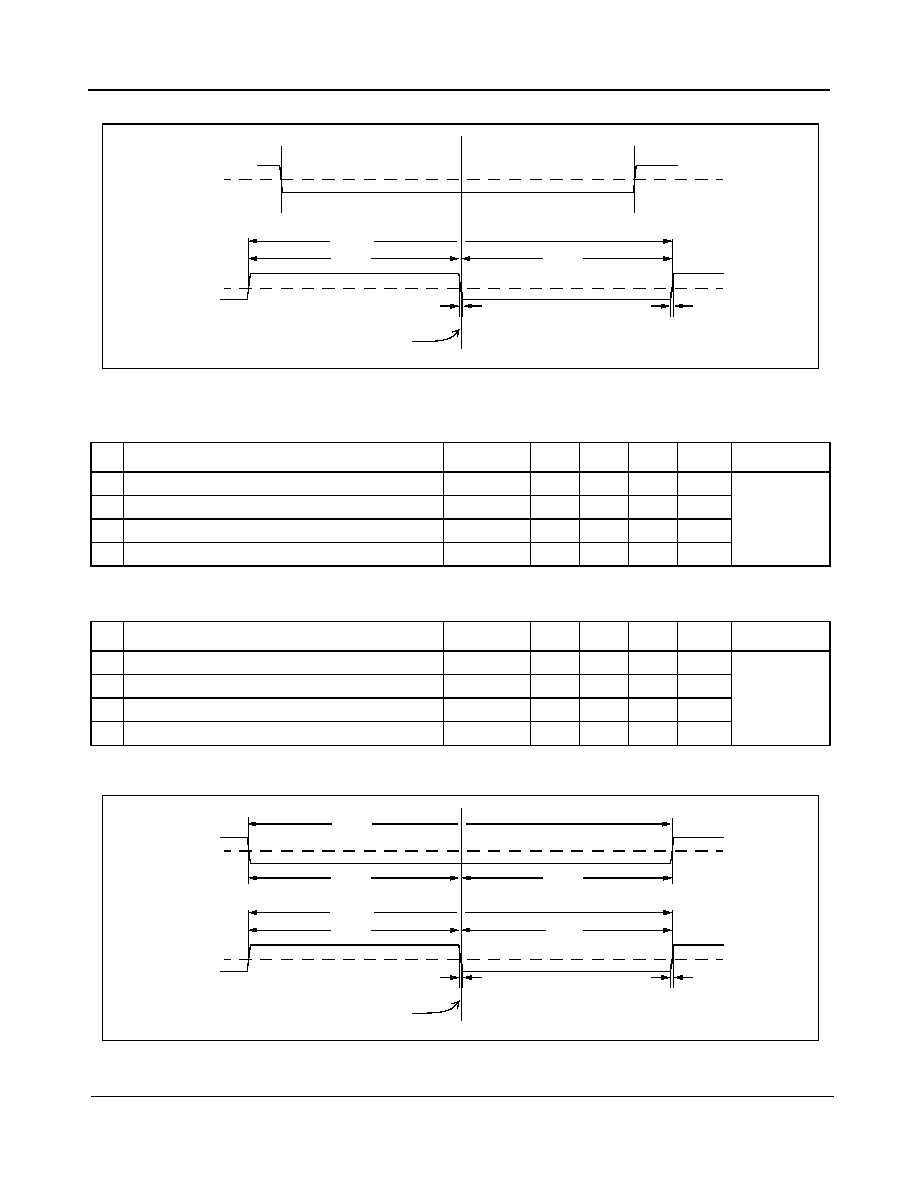
ZL50015
Data Sheet
112
Zarlink Semiconductor Inc.
Figure 46 - FPo4 and CKo4 Timing Diagram (1.544/2.048 MHz)
Characteristics are over recommended operating conditions unless otherwise stated.
Typical figures are at 25
∞C and are for design aid only: not guaranteed and not subject to production testing.
Figure 47 - CKo5 Timing Diagram (19.44 MHz)
AC Electrical Characteristics
- CKo4 (1.544 MHz) Timing (Only when DPLL is active)
Characteristic
Sym.
Min. Typ.
Max.
Units
Notes
1
CKo4 Output Clock Period
t
CKP4
645
648
650
ns
C
L
= 30 pF
2
CKo4 Output High Time
t
CKH4
320
324
327
ns
3
CKo4 Output Low Time
t
CKL4
320
324
327
ns
4
CKo4 Output Rise/Fall Time
t
rCK4
, t
fCK4
5
ns
AC Electrical Characteristics
- CKo4 (2.048 MHz) Timing (Only when DPLL is active)
Characteristic
Sym.
Min. Typ.
Max.
Units
Notes
1
CKo4 Output Clock Period
t
CKP4
485
488
492
ns
C
L
= 30 pF
2
CKo4 Output High Time
t
CKH4
241
244
247
ns
3
CKo4 Output Low Time
t
CKL4
241
244
247
ns
4
CKo4 Output Rise/Fall Time
t
rCK4
, t
fCK4
5
ns
FPo0
CKo4
t
CKL4
t
CKH4
t
CKP4
t
rCK4
t
fCK4
Output Frame Boundary
V
CT
V
CT
t
FPW5
t
FODR5
t
FODF5
FPo5
CKo5
t
CKH5
t
CKP5
t
rCK5
t
fCK5
Output Frame Boundary
V
CT
V
CT
(shares output pin
with FPo_OFF2)
t
CKL5
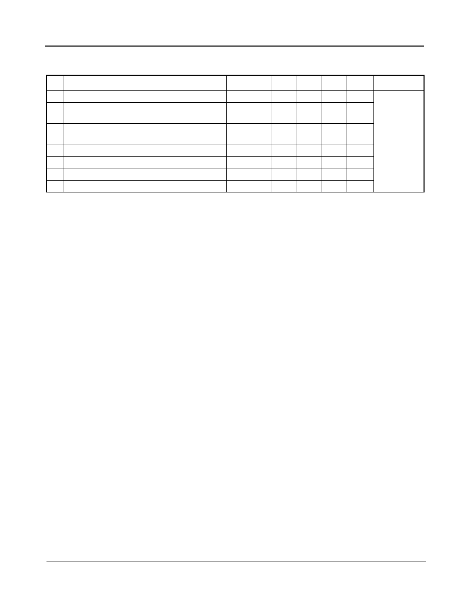
ZL50015
Data Sheet
113
Zarlink Semiconductor Inc.
Characteristics are over recommended operating conditions unless otherwise stated.
Typical figures are at 25
∞C and are for design aid only: not guaranteed and not subject to production testing.
AC Electrical Characteristics
- CKo5 (19.44 MHz) Timing (Only when DPLL is active)
Characteristic
Sym.
Min. Typ.
Max.
Units
Notes
1
FPo5 Output Pulse Width
t
FPW5
49
51
55
ns
C
L
= 30 pF
2
FPo5 Output Delay from the FPo5 falling edge
to the output frame boundary
t
FODF5
22
25
28
ns
3
FPo5 Output Delay from the output frame
boundary to the FPo5 rising edge
t
FODR5
21
25
32
ns
4
CKo5 Output Clock Period
t
CKP5
50
51
53
ns
5
CKo5 Output High Time
t
CKH5
23
25
27
ns
6
CKo5 Output Low Time
t
CKL5
24
25
28
ns
7
CKo5 Output Rise/Fall Time
t
rCK5
, t
fCK5
5
ns
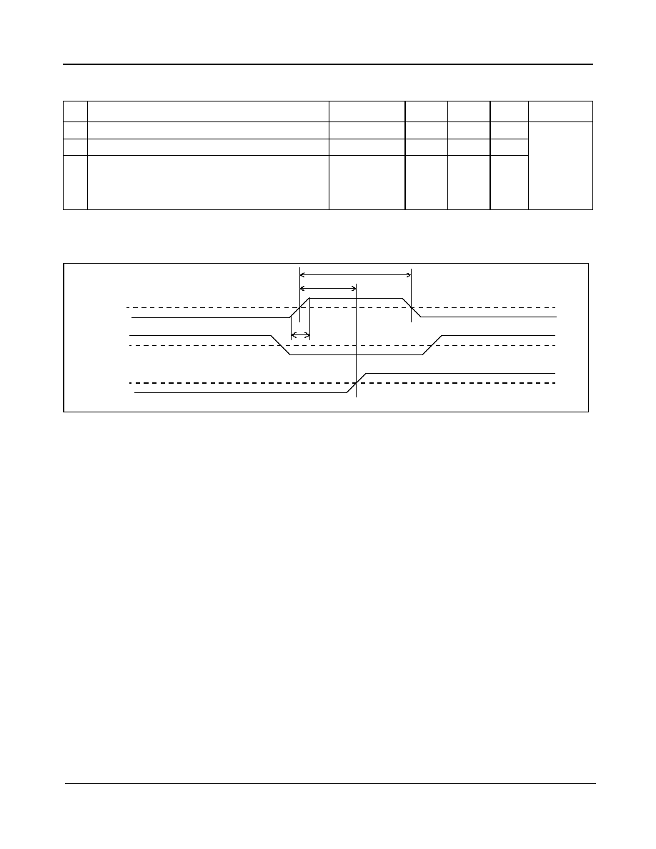
ZL50015
Data Sheet
114
Zarlink Semiconductor Inc.
Characteristics are over recommended operating conditions unless otherwise stated.
See "Performance Characteristics Notes" on page 119.
Figure 48 - REF0 - 3 Reference Input/Output Timing
AC Electrical Characteristics
- REF0-3 Reference Input to CKo Output Timing
Characteristic
Sym.
Min.
Max.
Units
Notes
1
Minimum Input Pulse Width High or Low
t
RPMIN
16
ns
1,2,3,14
2
Input Rise or Fall Time
t
IR
, (or t
IF
)
5
ns
3
REF input to CKo0 output delay (no input jitter)
REF @ 8 kHz, 2.048, 4.096, 8.192, 16.384 MHz
REF @ 1.544 MHz
REF @ 19.44 MHz
t
RD
-7
6
-10
0
15
-2
ns
ns
ns
FPo[n]
CKo[n]
V
CT
REF0-3
t
RD
V
CT
V
CT
t
IR
t
RPMIN
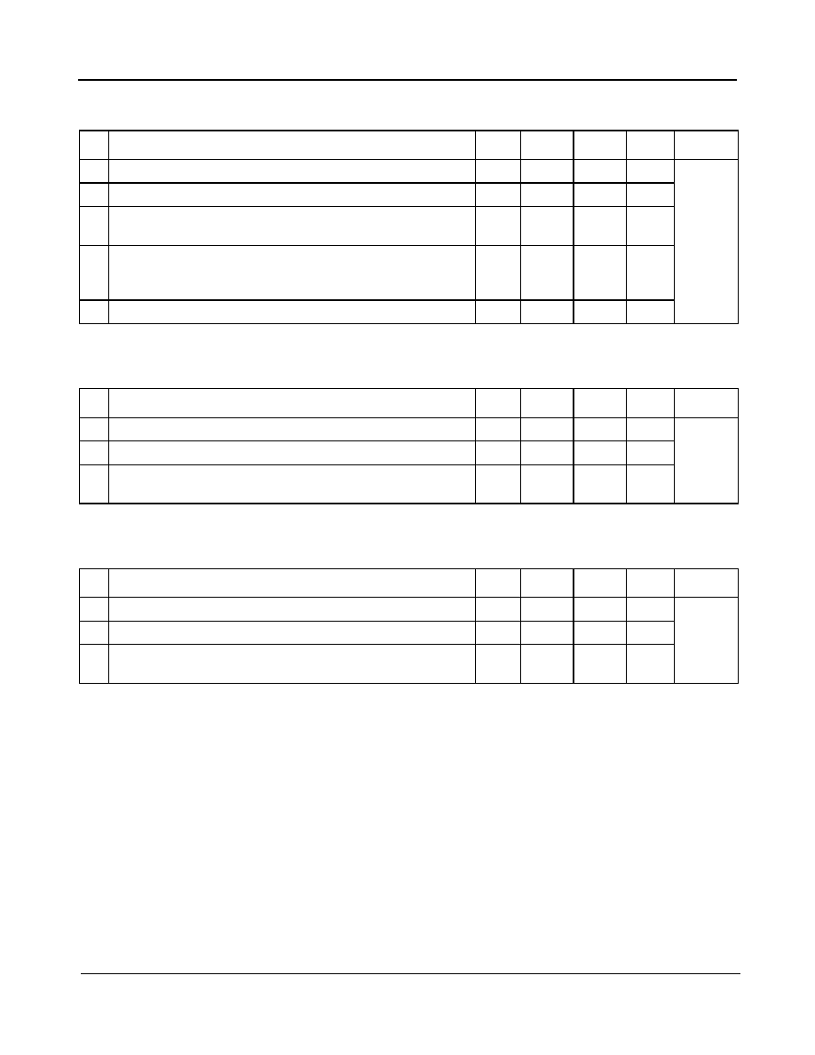
ZL50015
Data Sheet
115
Zarlink Semiconductor Inc.
Characteristics are over recommended operating conditions unless otherwise stated.
See "Performance Characteristics Notes" on page 119.
Characteristics are over recommended operating conditions unless otherwise stated.
See "Performance Characteristics Notes" on page 119.
Characteristics are over recommended operating conditions unless otherwise stated.
See "Performance Characteristics Notes" on page 119.
AC Electrical Characteristics
- Master Mode Output Timing
Characteristic
Sym.
Min.
Max.
Units
Notes
1
CKo0 to CKo1 (8.192 MHz) delay
t
C1D
-1
2
ns
1-5,14
2
CKo0 to CKo2 (16.384 MHz) delay
t
C2D
-1
3
ns
3
CKo0 to CKo3
(32.768 MHz/16.384 MHz/8.192 MHz/4.096 MHz) delay
t
C3D
-4
0
ns
4
CKo0 to CKo4 (1.544 MHz/2.048 MHz) delay
CKo4 @ 1.544 MHz
CKo4 @ 2.048 MHz
t
C4D
-12
-2
-7
3
ns
ns
5
CKo0 to CKo5 (19.44 MHz) delay
t
C5D
6
12
ns
AC Electrical Characteristics
- Divided Slave Mode Output Timing
Characteristic
Sym.
Min.
Max.
Units
Notes
1
CKo0 to CKo1 (8.192 MHz) delay
t
C1D
-1
2
ns
1-5,14
2
CKo0 to CKo2 (16.384 MHz) delay
t
C2D
-1
3
ns
3
CKo0 to CKo3
(16.384 MHz/8.192 MHz/4.096 MHz) delay
t
C3D
-2
2
ns
AC Electrical Characteristics
- Multiplied Slave Mode Output Timing
Characteristic
Sym.
Min.
Max.
Units
Notes
1
CKo0 to CKo1 (8.192 MHz) delay
t
C1D
-1
2
ns
1-5,14
2
CKo0 to CKo2 (16.384 MHz) delay
t
C2D
-1
3
ns
3
CKo0 to CKo3
(32.768 MHz/16.384 MHz/8.192 MHz/4.096 MHz) delay
t
C3D
-1
3
ns
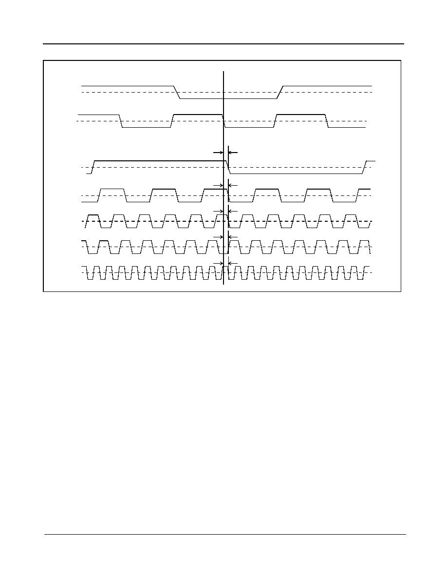
ZL50015
Data Sheet
116
Zarlink Semiconductor Inc.
Figure 49 - Output Timing (ST-BUS Format)
FPo0
CKo1
CKo0
V
CT
CKo2
CKo3
CKo4
CKo5
V
CT
V
CT
V
CT
V
CT
V
CT
V
CT
t
C1D
t
C2D
t
C5D
t
C3D
(1.544 MHz)
(4.096 MHz)
(8.192 MHz)
(16.384 MHz)
(32.768 MHz)
(19.44 MHz)
t
C4D
ZL50015
Data Sheet
117
Zarlink Semiconductor Inc.
Characteristics are over recommended operating conditions unless otherwise stated.
See "Performance Characteristics Notes" on page 119.
DPLL Performance Characteristics - Accuracy & Switching
Characteristics
Min.
Max.
Units
Conditions/
Notes
1
Freerun Accuracy
-0.003
0
ppm
1,5,7
2
Initial Holdover Frequency Stability
-0.03
0.03
ppm
1,4,8
3
Pull-in/Hold-in Range (Stratum 4E)
-260
260
ppm
1,3,7,9
4
Reference Far Hysteresis Limit (Stratum 4E)
-82.5
82.5
ppm
1,3,7,9,12
5
Reference Near Hysteresis Limit (Stratum 4E)
-64.5
64.5
ppm
6
Reference Far Hysteresis Limit (Relaxed Stratum 4E)
-248
248
ppm
1,3,7,9,13
7
Reference Near Hysteresis Limit (Relaxed Stratum 4E)
-242
242
ppm
8
Output phase continuity for reference switch
1
1. Reference switching to normal, holdover, or freerun mode
31
ns
11
9
Normal output phase alignment speed (phase slope)
56
µs/s
10
10
Normal phase lock time
2
2. -32 to +32 ppm locking
75
s
1,3,7,9,10

ZL50015
Data Sheet
118
Zarlink Semiconductor Inc.
Characteristics are over recommended operating conditions unless otherwise stated.
Typical figures are at 25
∞C and are for design aid only: not guaranteed and not subject to production testing.
* See "Performance Characteristics Notes" on page 119.
DPLL Performance Characteristics - Output Jitter Generation (Unfiltered except for CKo5)
Characteristics
Typ.
Units
Conditions/Notes*
1
Jitter at CKo0 and CKo3 (4.096 MHz)
810
ps-pp
1-6,14
2
Jitter at CKo1 and CKo3 (8.192 MHz)
800
ps-pp
3
Jitter at CKo2 and CKo3 (16.384 MHz)
710
ps-pp
4
Jitter at CKo3 (4.096, 8.192, 16.384, or 32.768 MHz)
670
ps-pp
5
Jitter at CKo4 (1.544 MHz or 2.048 MHz)
1.544 MHz
2.048 MHz
1060
630
ps-pp
ps-pp
6
Jitter at CKo5 (19.44 MHz)
unfiltered jitter
500 Hz - 1.3 MHz jitter
65 kHz - 1.3 MHz jitter
12 kHz - 1.3 MHz jitter
770
540
460
510
ps-pp
ps-pp
ps-pp
ps-pp

ZL50015
Data Sheet
119
Zarlink Semiconductor Inc.
Performance Characteristics Notes
Characteristics are over recommended operating conditions unless otherwise stated.
Typical figures are at 25
∞C, V
DD_CORE
at 1.8 V and V
DD_IO
at 3.3 V and are for design aid only: not guaranteed and not subject to production
testing.
1. Jitter on master clock input (XIN) is 100 ps pp or less.
2. Jitter on reference input (REF0-3) is 2 ns pp or less.
3. Normal Mode selected.
4. Holdover Mode selected.
5. Freerun Mode selected.
6. Jitter is measured without an output filter.
7. Accuracy of master clock input (XIN) is 0
ppm
.
8. Accuracy of master clock input (XIN) is 100
ppm
.
9. Capture range is +/-260 ppm; inaccuracy of XIN shifts this range.
10. Phase alignment speed (phase slope) is programmed to 7 ns/125
µ
s.
11. Any input reference switch or state switch (i.e. REF0 to REF3, Normal to Holdover, etc.).
12. Multi-period near limits and far limits are programmed to +/-64.713ppm & +/-82.487ppm respectively. (ST4_LIM = 1)
13. Multi-period near limits and far limits are programmed to +/-240ppm & +/-250ppm respectively. (ST4_LIM = 0)
14. 30 pF load on output pin.
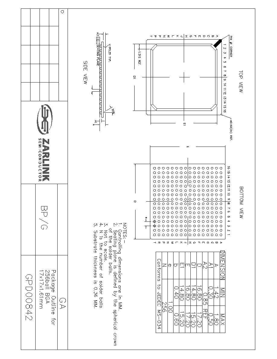
c Zarlink Semiconductor 2003 All rights reserved.
APPRD.
ISSUE
DATE
ACN
Package Code
Previous package codes
b
214440
1
26June03
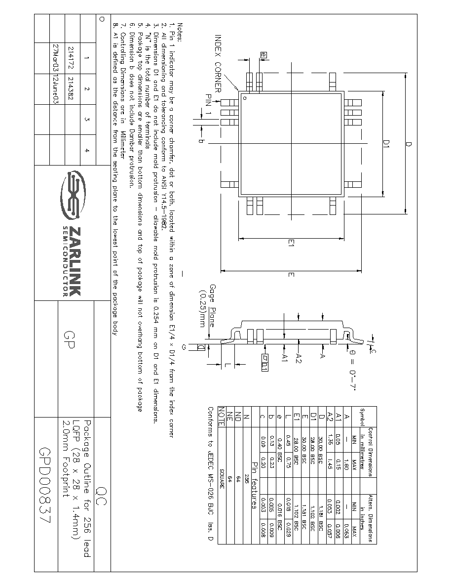
c Zarlink Semiconductor 2003 All rights reserved.
APPRD.
ISSUE
DATE
ACN
Package Code
Previous package codes

www.zarlink.com
Information relating to products and services furnished herein by Zarlink Semiconductor Inc. or its subsidiaries (collectively "Zarlink") is believed to be reliable.
However, Zarlink assumes no liability for errors that may appear in this publication, or for liability otherwise arising from the application or use of any such
information, product or service or for any infringement of patents or other intellectual property rights owned by third parties which may result from such application or
use. Neither the supply of such information or purchase of product or service conveys any license, either express or implied, under patents or other intellectual
property rights owned by Zarlink or licensed from third parties by Zarlink, whatsoever. Purchasers of products are also hereby notified that the use of product in
certain ways or in combination with Zarlink, or non-Zarlink furnished goods or services may infringe patents or other intellectual property rights owned by Zarlink.
This publication is issued to provide information only and (unless agreed by Zarlink in writing) may not be used, applied or reproduced for any purpose nor form part
of any order or contract nor to be regarded as a representation relating to the products or services concerned. The products, their specifications, services and other
information appearing in this publication are subject to change by Zarlink without notice. No warranty or guarantee express or implied is made regarding the
capability, performance or suitability of any product or service. Information concerning possible methods of use is provided as a guide only and does not constitute
any guarantee that such methods of use will be satisfactory in a specific piece of equipment. It is the user's responsibility to fully determine the performance and
suitability of any equipment using such information and to ensure that any publication or data used is up to date and has not been superseded. Manufacturing does
not necessarily include testing of all functions or parameters. These products are not suitable for use in any medical products whose failure to perform may result in
significant injury or death to the user. All products and materials are sold and services provided subject to Zarlink's conditions of sale which are available on request.
Purchase of Zarlink's I
2
C components conveys a licence under the Philips I
2
C Patent rights to use these components in and I
2
C System, provided that the system
conforms to the I
2
C Standard Specification as defined by Philips.
Zarlink, ZL and the Zarlink Semiconductor logo are trademarks of Zarlink Semiconductor Inc.
Copyright Zarlink Semiconductor Inc. All Rights Reserved.
TECHNICAL DOCUMENTATION - NOT FOR RESALE
For more information about all Zarlink products
visit our Web Site at