 | –≠–ї–µ–Ї—В—А–Њ–љ–љ—Л–є –Ї–Њ–Љ–њ–Њ–љ–µ–љ—В: ZL50017 | –°–Ї–∞—З–∞—В—М:  PDF PDF  ZIP ZIP |
Document Outline
- Features
- Applications
- Description
- Figure 1 - ZL50017 Functional Block Diagram
- Changes Summary
- 1.0 Pinout Diagrams
- 1.1 BGA Pinout
- Figure 2 - ZL50017 256-Ball 17 mm x 17 mm PBGA (as viewed through top of package)
- 1.2 QFP Pinout
- Figure 3 - ZL50017 256-Lead 28 mm x 28 mm LQFP (top view)
- 2.0 Pin Description
- 3.0 Device Overview
- 4.0 Data Rates and Timing
- 4.1 Input Clock (CKi) and Input Frame Pulse (FPi) Timing
- Figure 4 - Input Timing when CKIN1 - 0 bits = Н10О in the CR
- Figure 5 - Input Timing when CKIN1 - 0 bits = Н01О in the CR
- Figure 6 - Input Timing when CKIN1 - 0 = Н00О in the CR
- 4.2 ST-BUS and GCI-Bus Timing
- 5.0 Data Input Delay and Data Output Advancement
- 5.1 Input Bit Delay Programming
- Figure 7 - Input Bit Delay Timing Diagram (ST-BUS)
- 5.2 Input Bit Sampling Point Programming
- Figure 8 - Input Bit Sampling Point Programming
- Figure 9 - Input Bit Delay and Factional Sampling Point
- 5.3 Output Advancement Programming
- Figure 10 - Output Bit Advancement Timing Diagram (ST-BUS)
- 5.4 Fractional Output Bit Advancement Programming
- Figure 11 - Output Fractional Bit Advancement Timing Diagram (ST-BUS)
- 6.0 Data Delay Through the Switching Paths
- 6.1 Variable Delay Mode
- Table 1 - Delay for Variable Delay Mode
- Figure 12 - Data Throughput Delay for Variable Delay
- 6.2 Constant Delay Mode
- Figure 13 - Data Throughput Delay for Constant Delay
- 7.0 Connection Memory Description
- 8.0 Connection Memory Block Programming
- 8.1 Memory Block Programming Procedure
- Table 2 - Connection Memory Low After Block Programming
- 9.0 Microprocessor Port
- 10.0 Device Reset and Initialization
- 10.1 Power-up Sequence
- 10.2 Device Initialization on Reset
- 10.3 Software Reset
- 11.0 JTAG Port
- 11.1 Test Access Port (TAP)
- 11.2 Instruction Register
- 11.3 Test Data Registers
- 11.4 BSDL
- 12.0 Register Address Mapping
- Table 3 - Address Map for Registers (A13 = 0)
- 13.0 Detailed Register Description
- Table 4 - Control Register (CR) Bits
- Table 5 - Internal Mode Selection Register (IMS) Bits
- Table 6 - Software Reset Register (SRR) Bits
- Table 7 - Data Rate Selection Register
- Table 8 - Internal Flag Register (IFR) Bits - Read Only
- Table 9 - Stream Input Control Register 0 - 15 (SICR0 - 15) Bits
- Table 10 - Stream Output Control Register 0 - 15 (SOCR0 - 15) Bits
- 14.0 Memory
- 14.1 Memory Address Mappings
- Table 11 - Address Map for Memory Locations (A13 = 1)
- 14.2 Connection Memory Low (CM_L) Bit Assignment
- Table 12 - Connection Memory Low (CM_L) Bit Assignment when CMM = 0
- Table 13 - Connection Memory Low (CM_L) Bit Assignment when CMM = 1
- 15.0 DC Parameters
- Absolute Maximum Ratings*
- Recommended Operating Conditions - Voltages are with respect to ground (VSS) unless otherwise stated.
- DC Electrical CharacteristicsБ - Voltages are with respect to ground (Vss) unless otherwise stated.
- 16.0 AC Parameters
- AC Electrical CharacteristicsБ - Timing Parameter Measurement Voltage Levels
- Figure 14 - Timing Parameter Measurement Voltage Levels
- AC Electrical CharacteristicsБ - Motorola Non-Multiplexed Bus Mode - Read Access
- Figure 15 - Motorola Non-Multiplexed Bus Timing - Read Access
- AC Electrical CharacteristicsБ - Motorola Non-Multiplexed Bus Mode - Write Access
- Figure 16 - Motorola Non-Multiplexed Bus Timing - Write Access
- AC Electrical CharacteristicsБ - Intel Non-Multiplexed Bus Mode - Read Access
- Figure 17 - Intel Non-Multiplexed Bus Timing - Read Access
- AC Electrical CharacteristicsБ - Intel Non-Multiplexed Bus Mode - Write Access
- Figure 18 - Intel Non-Multiplexed Bus Timing - Write Access
- AC Electrical CharacteristicsБ - JTAG Test Port Timing
- Figure 19 - JTAG Test Port Timing Diagram
- AC Electrical CharacteristicsБ - FPi and CKi Timing when CKIN1-0 bits = 00 (16.384 MHz)
- AC Electrical CharacteristicsБ - FPi and CKi Timing when CKIN1-0 bits = 01 (8.192 MHz)
- AC Electrical CharacteristicsБ- FPi and CKi Timing when CKIN1-0 bits = 10 (4.096 MHz)
- Figure 20 - Frame Pulse Input and Clock Input Timing Diagram (ST-BUS)
- Figure 21 - Frame Pulse Input and Clock Input Timing Diagram (GCI-Bus)
- AC Electrical CharacteristicsБ - ST-BUS/GCI-Bus Input Timing
- Figure 22 - ST-BUS Input and Output Timing Diagram when Operated at 2, 4, 8 and 16 Mbps
- Figure 23 - GCI-Bus Input and Output Timing Diagram when Operated at 2, 4, 8 and 16 Mbps

1
Zarlink Semiconductor Inc.
Zarlink, ZL and the Zarlink Semiconductor logo are trademarks of Zarlink Semiconductor Inc.
Copyright 2004-2006, Zarlink Semiconductor Inc. All Rights Reserved.
Features
Ј 1024 channel x 1024 channel non-blocking digital
Time Division Multiplex (TDM) switch at 4.096,
8.192 or 16.384 Mbps
Ј 16 serial TDM input, 16 serial TDM output
streams
Ј Output streams can be configured as bi-
directional for connection to backplanes
Ј Exceptional input clock cycle to cycle variation
tolerance (20 ns for all rates)
Ј Per-stream input bit delay with flexible sampling
point selection
Ј Per-stream output bit and fractional bit
advancement
Ј Per-channel constant or variable throughput
delay for frame integrity and low latency
applications
Ј Per-channel high impedance output control
Ј Per-channel message mode
Ј Input clock: 4.096 MHz, 8.192 MHz, 16.384 MHz
Ј Input frame pulses:61 ns, 122 ns, 244 ns
Ј Control interface compatible with Intel and
Motorola 16-bit non-multiplexed buses
Ј Connection memory block programming
Ј Supports ST-BUS and GCI-Bus standards for
input and output timing
Ј IEEE-1149.1 (JTAG) test port
Ј 3.3 V I/O with 5 V tolerant inputs; 1.8 V core
voltage
Applications
Ј PBX and IP-PBX
Ј Small and medium digital switching platforms
Ј Remote access servers and concentrators
Ј Wireless base stations and controllers
Ј Multi service access platforms
Ј Digital Loop Carriers
Ј Computer Telephony Integration
January 2006
Ordering Information
ZL50017GAC
256 Ball PBGA
Trays
ZL50017QCC
256 Lead LQFP
Trays
ZL50017GAG2
256 Ball PBGA**
Trays
**Pb Free Tin/Silver/Copper
-40
∞C to +85∞C
ZL50017
1 K Digital Switch
Data Sheet
Figure 1 - ZL50017 Functional Block Diagram
Data Memory
Te
s
t
P
o
r
t
S/P Converter
STio[15:0]
M
O
T_
IN
TE
L
DS
_RD
CS
D[15:
0
]
A[
13:
0]
TMS
TDi
TDo
TCK
TRST
STi[15:0]
P/S Converter
DT
A
_RDY
R/W
_W
R
Connection Memory
Internal Registers &Microprocessor Interface
Input Timing
FPi
CKi
MODE_4M0
MODE_4M1
ODE
RESET
V
SS
V
DD_IO
V
DD_CORE
V
DD_IOA
V
DD_COREA

ZL50017
Data Sheet
2
Zarlink Semiconductor Inc.
Description
The ZL50017 is a maximum 1024 x 1024 channel non-blocking digital Time Division Multiplex (TDM) switch. It has
sixteen input streams (STi0 - 15) and sixteen output streams (STio0 - 15). The device can switch 64 kbps and
Nx64 kbps TDM channels from any input stream to any output stream. All of the input and output streams operate
at the same data rate and can be programmed at any of the following data rates: 2.048 Mbps, 4.096 Mbps,
8.192 Mbps or 16.384 Mbps. The output streams can be configured to operate in bi-directional mode, in which case
STi0 - 15 will be ignored.
The device contains two types of internal memory - data memory and connection memory. There are three modes
of operation - Connection Mode, Message Mode and high impedance mode. In Connection Mode, the contents of
the connection memory define, for each output stream and channel, the source stream and channel (the actual
data to be output is stored in the data memory). In Message Mode, the connection memory is used for the storage
of microprocessor data. Using Zarlink's Message Mode capability, microprocessor data can be broadcast to the
data output streams on a per-channel basis. This feature is useful for transferring control and status information for
external circuits or other TDM devices. In high impedance mode the selected output channel can be put into a high
impedance state.
The configurable non-multiplexed microprocessor port allows users to program various device operating modes
and switching configurations. Users can employ the microprocessor port to perform register read/write, connection
memory read/write and data memory read operations. The port is configurable to interface with either Motorola or
Intel-type microprocessors.
The device also supports the mandatory requirements of the IEEE-1149.1 (JTAG) standard via the test port.

ZL50017
Data Sheet
Table of Contents
3
Zarlink Semiconductor Inc.
Features . . . . . . . . . . . . . . . . . . . . . . . . . . . . . . . . . . . . . . . . . . . . . . . . . . . . . . . . . . . . . . . . . . . . . . . . . . . . . . . . . 1
Applications . . . . . . . . . . . . . . . . . . . . . . . . . . . . . . . . . . . . . . . . . . . . . . . . . . . . . . . . . . . . . . . . . . . . . . . . . . . . . 1
Description . . . . . . . . . . . . . . . . . . . . . . . . . . . . . . . . . . . . . . . . . . . . . . . . . . . . . . . . . . . . . . . . . . . . . . . . . . . . . . 2
Changes Summary . . . . . . . . . . . . . . . . . . . . . . . . . . . . . . . . . . . . . . . . . . . . . . . . . . . . . . . . . . . . . . . . . . . . . . . . 6
1.0 Pinout Diagrams . . . . . . . . . . . . . . . . . . . . . . . . . . . . . . . . . . . . . . . . . . . . . . . . . . . . . . . . . . . . . . . . . . . . . . . 7
1.1 BGA Pinout . . . . . . . . . . . . . . . . . . . . . . . . . . . . . . . . . . . . . . . . . . . . . . . . . . . . . . . . . . . . . . . . . . . . . . . . . 7
1.2 QFP Pinout . . . . . . . . . . . . . . . . . . . . . . . . . . . . . . . . . . . . . . . . . . . . . . . . . . . . . . . . . . . . . . . . . . . . . . . . . 8
2.0 Pin Description. . . . . . . . . . . . . . . . . . . . . . . . . . . . . . . . . . . . . . . . . . . . . . . . . . . . . . . . . . . . . . . . . . . . . . . . . 9
3.0 Device Overview . . . . . . . . . . . . . . . . . . . . . . . . . . . . . . . . . . . . . . . . . . . . . . . . . . . . . . . . . . . . . . . . . . . . . . 14
4.0 Data Rates and Timing . . . . . . . . . . . . . . . . . . . . . . . . . . . . . . . . . . . . . . . . . . . . . . . . . . . . . . . . . . . . . . . . . 14
4.1 Input Clock (CKi) and Input Frame Pulse (FPi) Timing . . . . . . . . . . . . . . . . . . . . . . . . . . . . . . . . . . . . . . . 15
4.2 ST-BUS and GCI-Bus Timing . . . . . . . . . . . . . . . . . . . . . . . . . . . . . . . . . . . . . . . . . . . . . . . . . . . . . . . . . . 17
5.0 Data Input Delay and Data Output Advancement . . . . . . . . . . . . . . . . . . . . . . . . . . . . . . . . . . . . . . . . . . . . 17
5.1 Input Bit Delay Programming. . . . . . . . . . . . . . . . . . . . . . . . . . . . . . . . . . . . . . . . . . . . . . . . . . . . . . . . . . . 18
5.2 Input Bit Sampling Point Programming . . . . . . . . . . . . . . . . . . . . . . . . . . . . . . . . . . . . . . . . . . . . . . . . . . . 19
5.3 Output Advancement Programming . . . . . . . . . . . . . . . . . . . . . . . . . . . . . . . . . . . . . . . . . . . . . . . . . . . . . 20
5.4 Fractional Output Bit Advancement Programming . . . . . . . . . . . . . . . . . . . . . . . . . . . . . . . . . . . . . . . . . . 21
6.0 Data Delay Through the Switching Paths . . . . . . . . . . . . . . . . . . . . . . . . . . . . . . . . . . . . . . . . . . . . . . . . . . 22
6.1 Variable Delay Mode . . . . . . . . . . . . . . . . . . . . . . . . . . . . . . . . . . . . . . . . . . . . . . . . . . . . . . . . . . . . . . . . . 22
6.2 Constant Delay Mode . . . . . . . . . . . . . . . . . . . . . . . . . . . . . . . . . . . . . . . . . . . . . . . . . . . . . . . . . . . . . . . . 23
7.0 Connection Memory Description . . . . . . . . . . . . . . . . . . . . . . . . . . . . . . . . . . . . . . . . . . . . . . . . . . . . . . . . . 23
8.0 Connection Memory Block Programming . . . . . . . . . . . . . . . . . . . . . . . . . . . . . . . . . . . . . . . . . . . . . . . . . . 24
8.1 Memory Block Programming Procedure . . . . . . . . . . . . . . . . . . . . . . . . . . . . . . . . . . . . . . . . . . . . . . . . . . 24
9.0 Microprocessor Port . . . . . . . . . . . . . . . . . . . . . . . . . . . . . . . . . . . . . . . . . . . . . . . . . . . . . . . . . . . . . . . . . . . 24
10.0 Device Reset and Initialization . . . . . . . . . . . . . . . . . . . . . . . . . . . . . . . . . . . . . . . . . . . . . . . . . . . . . . . . . . 25
10.1 Power-up Sequence . . . . . . . . . . . . . . . . . . . . . . . . . . . . . . . . . . . . . . . . . . . . . . . . . . . . . . . . . . . . . . . . 25
10.2 Device Initialization on Reset . . . . . . . . . . . . . . . . . . . . . . . . . . . . . . . . . . . . . . . . . . . . . . . . . . . . . . . . . 25
10.3 Software Reset . . . . . . . . . . . . . . . . . . . . . . . . . . . . . . . . . . . . . . . . . . . . . . . . . . . . . . . . . . . . . . . . . . . . 25
11.0 JTAG Port . . . . . . . . . . . . . . . . . . . . . . . . . . . . . . . . . . . . . . . . . . . . . . . . . . . . . . . . . . . . . . . . . . . . . . . . . . . 25
11.1 Test Access Port (TAP) . . . . . . . . . . . . . . . . . . . . . . . . . . . . . . . . . . . . . . . . . . . . . . . . . . . . . . . . . . . . . . 25
11.2 Instruction Register . . . . . . . . . . . . . . . . . . . . . . . . . . . . . . . . . . . . . . . . . . . . . . . . . . . . . . . . . . . . . . . . . 26
11.3 Test Data Registers. . . . . . . . . . . . . . . . . . . . . . . . . . . . . . . . . . . . . . . . . . . . . . . . . . . . . . . . . . . . . . . . . 26
11.4 BSDL . . . . . . . . . . . . . . . . . . . . . . . . . . . . . . . . . . . . . . . . . . . . . . . . . . . . . . . . . . . . . . . . . . . . . . . . . . . . 26
12.0 Register Address Mapping . . . . . . . . . . . . . . . . . . . . . . . . . . . . . . . . . . . . . . . . . . . . . . . . . . . . . . . . . . . . . 27
13.0 Detailed Register Description . . . . . . . . . . . . . . . . . . . . . . . . . . . . . . . . . . . . . . . . . . . . . . . . . . . . . . . . . . . 28
14.0 Memory . . . . . . . . . . . . . . . . . . . . . . . . . . . . . . . . . . . . . . . . . . . . . . . . . . . . . . . . . . . . . . . . . . . . . . . . . . . . . 34
14.1 Memory Address Mappings. . . . . . . . . . . . . . . . . . . . . . . . . . . . . . . . . . . . . . . . . . . . . . . . . . . . . . . . . . . 34
14.2 Connection Memory Low (CM_L) Bit Assignment. . . . . . . . . . . . . . . . . . . . . . . . . . . . . . . . . . . . . . . . . . 35
15.0 DC Parameters . . . . . . . . . . . . . . . . . . . . . . . . . . . . . . . . . . . . . . . . . . . . . . . . . . . . . . . . . . . . . . . . . . . . . . . 37
16.0 AC Parameters . . . . . . . . . . . . . . . . . . . . . . . . . . . . . . . . . . . . . . . . . . . . . . . . . . . . . . . . . . . . . . . . . . . . . . . 38

ZL50017
Data Sheet
List of Figures
4
Zarlink Semiconductor Inc.
Figure 1 - ZL50017 Functional Block Diagram . . . . . . . . . . . . . . . . . . . . . . . . . . . . . . . . . . . . . . . . . . . . . . . . . . . . 1
Figure 2 - ZL50017 256-Ball 17 mm x 17 mm PBGA (as viewed through top of package) . . . . . . . . . . . . . . . . . . . 7
Figure 3 - ZL50017 256-Lead 28 mm x 28 mm LQFP (top view). . . . . . . . . . . . . . . . . . . . . . . . . . . . . . . . . . . . . . . 8
Figure 4 - Input Timing when CKIN1 - 0 bits = "10" in the CR . . . . . . . . . . . . . . . . . . . . . . . . . . . . . . . . . . . . . . . . 15
Figure 5 - Input Timing when CKIN1 - 0 bits = "01" in the CR . . . . . . . . . . . . . . . . . . . . . . . . . . . . . . . . . . . . . . . . 16
Figure 6 - Input Timing when CKIN1 - 0 = "00" in the CR . . . . . . . . . . . . . . . . . . . . . . . . . . . . . . . . . . . . . . . . . . . 16
Figure 7 - Input Bit Delay Timing Diagram (ST-BUS). . . . . . . . . . . . . . . . . . . . . . . . . . . . . . . . . . . . . . . . . . . . . . . 18
Figure 8 - Input Bit Sampling Point Programming . . . . . . . . . . . . . . . . . . . . . . . . . . . . . . . . . . . . . . . . . . . . . . . . . 19
Figure 9 - Input Bit Delay and Factional Sampling Point . . . . . . . . . . . . . . . . . . . . . . . . . . . . . . . . . . . . . . . . . . . . 20
Figure 10 - Output Bit Advancement Timing Diagram (ST-BUS) . . . . . . . . . . . . . . . . . . . . . . . . . . . . . . . . . . . . . . 21
Figure 11 - Output Fractional Bit Advancement Timing Diagram (ST-BUS). . . . . . . . . . . . . . . . . . . . . . . . . . . . . . 21
Figure 12 - Data Throughput Delay for Variable Delay . . . . . . . . . . . . . . . . . . . . . . . . . . . . . . . . . . . . . . . . . . . . . 22
Figure 13 - Data Throughput Delay for Constant Delay. . . . . . . . . . . . . . . . . . . . . . . . . . . . . . . . . . . . . . . . . . . . . 23
Figure 14 - Timing Parameter Measurement Voltage Levels. . . . . . . . . . . . . . . . . . . . . . . . . . . . . . . . . . . . . . . . . 38
Figure 15 - Motorola Non-Multiplexed Bus Timing - Read Access . . . . . . . . . . . . . . . . . . . . . . . . . . . . . . . . . . . . 39
Figure 16 - Motorola Non-Multiplexed Bus Timing - Write Access. . . . . . . . . . . . . . . . . . . . . . . . . . . . . . . . . . . . . 40
Figure 17 - Intel Non-Multiplexed Bus Timing - Read Access . . . . . . . . . . . . . . . . . . . . . . . . . . . . . . . . . . . . . . . . 41
Figure 18 - Intel Non-Multiplexed Bus Timing - Write Access . . . . . . . . . . . . . . . . . . . . . . . . . . . . . . . . . . . . . . . . 42
Figure 19 - JTAG Test Port Timing Diagram . . . . . . . . . . . . . . . . . . . . . . . . . . . . . . . . . . . . . . . . . . . . . . . . . . . . . 43
Figure 20 - Frame Pulse Input and Clock Input Timing Diagram (ST-BUS). . . . . . . . . . . . . . . . . . . . . . . . . . . . . . 45
Figure 21 - Frame Pulse Input and Clock Input Timing Diagram (GCI-Bus) . . . . . . . . . . . . . . . . . . . . . . . . . . . . . 45
Figure 22 - ST-BUS Input and Output Timing Diagram when Operated at 2, 4, 8 and 16 Mbps . . . . . . . . . . . . . . 47
Figure 23 - GCI-Bus Input and Output Timing Diagram when Operated at 2, 4, 8 and 16 Mbps . . . . . . . . . . . . . 48

ZL50017
Data Sheet
List of Tables
5
Zarlink Semiconductor Inc.
Table 1 - Delay for Variable Delay Mode . . . . . . . . . . . . . . . . . . . . . . . . . . . . . . . . . . . . . . . . . . . . . . . . . . . . . . . . 22
Table 2 - Connection Memory Low After Block Programming . . . . . . . . . . . . . . . . . . . . . . . . . . . . . . . . . . . . . . . . 24
Table 3 - Address Map for Registers (A13 = 0) . . . . . . . . . . . . . . . . . . . . . . . . . . . . . . . . . . . . . . . . . . . . . . . . . . . 27
Table 4 - Control Register (CR) Bits. . . . . . . . . . . . . . . . . . . . . . . . . . . . . . . . . . . . . . . . . . . . . . . . . . . . . . . . . . . . 28
Table 5 - Internal Mode Selection Register (IMS) Bits . . . . . . . . . . . . . . . . . . . . . . . . . . . . . . . . . . . . . . . . . . . . . . 30
Table 6 - Software Reset Register (SRR) Bits . . . . . . . . . . . . . . . . . . . . . . . . . . . . . . . . . . . . . . . . . . . . . . . . . . . . 31
Table 7 - Data Rate Selection Register . . . . . . . . . . . . . . . . . . . . . . . . . . . . . . . . . . . . . . . . . . . . . . . . . . . . . . . . . 31
Table 8 - Internal Flag Register (IFR) Bits - Read Only . . . . . . . . . . . . . . . . . . . . . . . . . . . . . . . . . . . . . . . . . . . . . 32
Table 9 - Stream Input Control Register 0 - 15 (SICR0 - 15) Bits. . . . . . . . . . . . . . . . . . . . . . . . . . . . . . . . . . . . . . 32
Table 10 - Stream Output Control Register 0 - 15 (SOCR0 - 15) Bits . . . . . . . . . . . . . . . . . . . . . . . . . . . . . . . . . . 33
Table 11 - Address Map for Memory Locations (A13 = 1) . . . . . . . . . . . . . . . . . . . . . . . . . . . . . . . . . . . . . . . . . . . 34
Table 12 - Connection Memory Low (CM_L) Bit Assignment when CMM = 0 . . . . . . . . . . . . . . . . . . . . . . . . . . . . 35
Table 13 - Connection Memory Low (CM_L) Bit Assignment when CMM = 1 . . . . . . . . . . . . . . . . . . . . . . . . . . . . 36

ZL50017
Data Sheet
6
Zarlink Semiconductor Inc.
Changes Summary
The following table captures the changes from the October 2004 issue.
Page
Item
Change
13
Pin Description "STio 0 - 15" on page 13
Ј Clarified STio 0-15 pin description.

ZL50017
Data Sheet
7
Zarlink Semiconductor Inc.
1.0 Pinout Diagrams
1.1 BGA Pinout
Figure 2 - ZL50017 256-Ball 17 mm x 17 mm PBGA (as viewed through top of package)
1
2
3
4
5
6
7
8
9
10
11
12
13
14
15
16
A
V
SS
NC
NC
NC
NC
NC
NC
NC
NC
NC
NC
NC
NC
NC
NC
V
SS
A
B
NC
STi10
STi5
STi4
NC
STi0
NC
NC
V
DD_
COREA
FPi
CKi
IC_Open IC_Open IC_GND
ODE
NC
B
C
NC
STi9
V
SS
STi7
STi6
STi1
NC
NC
V
SS
IC_Open IC_Open IC_Open IC_GND
V
SS
STio15
NC
C
D
NC
STi11
V
DD_IO
STi3
STi2
NC
NC
NC
NC
V
SS
NC
IC_GND
STio13
V
DD_IO
STio14
NC
D
E
NC
STi14
STi8
V
DD_IO
V
SS
V
DD_
CORE
NC
NC
NC
NC
V
DD_
CORE
V
SS
V
DD_IO
STio12
NC
NC
E
F
NC
STi15
STi12
STi13
V
DD_IO
V
DD_
CORE
V
DD_
CORE
V
SS
V
SS
V
DD_
CORE
V
DD_
CORE
V
DD_IO
IC_Open
NC
NC
NC
F
G
NC
RESET
IC_GND IC_Open
TDo
V
DD_IO
V
SS
V
SS
V
SS
V
SS
V
DD_IO
A12
A13
NC
NC
NC
G
H
NC
V
SS
V
SS
V
DD_
COREA
NC
V
SS
V
SS
V
SS
V
SS
V
SS
A7
A9
A10
NC
A11
NC
H
J
NC
V
DD_IOA
V
DD_IOA
V
SS
V
SS
NC
V
SS
V
SS
V
SS
V
SS
A3
A4
A5
A8
A6
NC
J
K
NC
V
SS
TMS
V
SS
V
DD_
COREA
V
DD_IO
V
SS
V
SS
V
SS
V
SS
V
DD_IO
IC_Open
A0
A2
A1
NC
K
L
NC
V
DD_
COREA
TRST
TCK
V
DD_IO
V
DD_
CORE
V
DD_
CORE
V
SS
V
SS
V
DD_
CORE
V
DD_
CORE
V
DD_IO
STio10
STio11
STio9
NC
L
M
NC
NC
TDi
D0
V
SS
V
DD_
CORE
V
DD_
CORE
D6
D10
V
DD_
CORE
V
DD_
CORE
V
SS
MOT
_INTEL
MODE_
4M0
STio8
NC
M
N
NC
NC
V
DD_IO
STio0
NC
D1
D5
D7
D11
D13
R/W
_WR
DTA_
RDY
STio4
V
DD_IO
NC
NC
N
P
NC
NC
V
SS
STio1
STio3
NC
D3
D8
D14
NC
STio5
NC
NC
V
SS
NC
NC
P
R
NC
NC
NC
STio2
NC
D2
D4
D9
D12
D15
CS
DS_RD
MODE_
4M1
STio6
STio7
NC
R
T
V
SS
NC
NC
NC
NC
NC
NC
NC
NC
NC
NC
NC
NC
NC
NC
V
SS
T
1
2
3
4
5
6
7
8
9
10
11
12
13
14
15
16
Note: A1 corner identified by metallized marking.
Note: Pinout is shown as viewed through top of package.

ZL50017
Data Sheet
8
Zarlink Semiconductor Inc.
1.2 QFP Pinout
Figure 3 - ZL50017 256-Lead 28 mm x 28 mm LQFP (top view)
152
154
156
158
160
162
164
166
168
170
172
174
176
178
180
22 24 26 28 30
20
18
16
14
12
10
8
6
4
2
120
102
104
106
108
110
114
116
118
112
52 54 56
58 60
50
48
46
44
42
40
38
36
34
32
100
82
84
86
88
90
94
96
98
92
80
66
68
70
74
76
78
72
132
134
136
138
140
142
144
146
148
150
CK
i
FP
i
IC_
O
p
e
n
IC_
O
p
e
n
IC_
O
p
e
n
IC_
O
p
e
n
IC_
G
ND
V
DD_
IO
VS
S
IC_
G
ND
OD
E
V
DD_
IO
NC NC NC NC
62 64
122
124
126
128
182
184
186
188
190
NC NC VS
S
VD
D
_
I
O
ST
i_7
ST
i_6
ST
i_
3
ST
i_
2
ST
i_
1
ST
i_
0
NC
VS
S
NC
NC
NC
NC
NC
NC
VS
S
NC
NC
ST
i_
5
ST
i_
4
VD
D
_
I
O
NC
NC
VS
S
V
D
D
_
CO
RE
NC
VSS
V
DD_
IO
NC
NC
VS
S
V
DD_
CO
RE
A
NC
VDD_IO
NC
NC
NC
NC
NC
NC
VDD_IO
TRST
TCK
TMS
VSS
VDD_CORE
VSS
VDD_COREA
VSS
VSS
NC
VDD_IOA
VDD_COREA
VSS
VSS
NC
VDD_IOA
VSS
VDD_COREA
VSS
VSS
VDD_CORE
TDo
RESET
IC_Open
IC_GND
VSS
VDD_IO
STi_15
STi_14
STi_11
STi_10
STi_9
STi_8
NC
NC
NC
VSS
TDi
NC
VDD_IO
NC
202
220
218
216
214
212
208
206
204
210
222
240
238
236
234
232
228
226
224
230
242
256
254
252
248
246
244
250
200
198
196
194
VSS
STi_13
STi_12
NC NC
NC
NC
VDD_I
O
VSS
S
T
i
o_0
S
T
i
o_1
S
T
i
o_2
S
T
i
o_3
NC NC NC
NC
VDD_I
O
VS
S
D0
V
D
D
_
CO
RE
VS
S
D1
D2
D3
D4 D5
D7 D8 D9
D6
VDD_I
O
VSS
D1
0
V
D
D
_
CO
RE
VS
S
D1
1
D1
2
D1
3
D1
4
D1
5
R/
W
_W
R
CS
M
O
T_I
N
TE
L
DS
_R
D
NC
DT
A
_RDY
MO
DE
_
4
M
0
V
D
D
_
CO
RE
VS
S
MO
D
E
_
4
M
1
VDD_I
O
VSS
S
T
i
o_4
S
T
i
o_5
S
T
i
o_6
S
T
i
o_7
NC NC
NC NC
V
DD_
I
O
VS
S
NC
NC
NC
NC
NC
VDD_IO
VSS
STio_8
STio_9
STio_10
STio_11
NC
NC
NC
NC
VDD_IO
IC_Open
VSS
VDD_CORE
VSS
A0
A1
A2
A3
A4
A7
A6
A5
A11
A10
A9
A8
VDD_CORE
VSS
A13
A12
IC_Open
VDD_IO
VSS
NC
NC
NC
NC
NC
NC
NC
VDD_CORE
VSS
IC_GND
VDD_IO
VSS
STio_12
STio_13
STio_14
STio_15
NC
NC
NC
NC
VDD_IO
VSS
NC
NC
NC
NC
NC
NC
NC
NC
NC
NC
NC
VS
S
V
DD_
CO
RE
VS
S
VS
S
V
DD_
IO
NC
NC
NC
NC
VSS
NC
NC
NC
192
130
NC
NC
NC
NC NC
NC
IC_
O
p
e
n

ZL50017
Data Sheet
9
Zarlink Semiconductor Inc.
2.0 Pin Description
PBGA Pin
Number
LQFP Pin
Number
Pin Name
Description
E6, E11, F6,
F7, F10,
F11, L6, L7,
L10, L11,
M6, M7,
M10, M11
19, 33,
45, 83,
95, 109,
146, 173,
213, 233
V
DD_CORE
Power Supply for the core logic: +1.8 V
H4, K5, B9,
L2
217, 231,
157, 224
V
DD_COREA
Power Supply for analog circuitry: +1.8 V
D3, D14, E4,
E13, F5,
F12, G6,
G11, K6,
K11, L5,
L12, N3,
N14
5, 15, 29,
49, 57,
69, 79,
101, 113,
121, 133,
143, 160,
169, 177,
186, 195,
207, 241,
249
V
DD_IO
Power Supply for I/O: +3.3 V
J2, J3
220, 226
V
DD_IOA
Power Supply for the CKo5 and CKo3 outputs: +3.3 V
A1, A16, C3,
C9, C14,
D10, E5,
E12, F8, F9,
G7, G8, G9,
G10, H2,
H3, H6, H7,
H8, H9,
H10, J4, J5,
J7, J8, J9,
J10, K2, K4,
K7, K8, K9,
K10, L8, L9,
M5, M12,
P3, P14, T1,
T16
8, 17, 21,
31, 35,
47, 50,
60, 71,
81, 85,
97, 103,
111, 114,
123, 142,
145, 147,
156, 158,
162, 171,
175, 178,
188, 199,
209, 214,
216, 218,
222, 223,
228, 230,
232, 235,
242, 251
V
SS
Ground

ZL50017
Data Sheet
10
Zarlink Semiconductor Inc.
K3
234
TMS
Test Mode Select (5 V-Tolerant Input with Internal Pull-up)
JTAG signal that controls the state transitions of the TAP
controller. This pin is pulled high by an internal pull-up resistor
when it is not driven.
L4
238
TCK
Test Clock (5 V-Tolerant Schmitt-Triggered Input with Internal
Pull-up)
Provides the clock to the JTAG test logic.
L3
239
TRST
Test Reset (5 V-Tolerant Input with Internal Pull-up)
Asynchronously initializes the JTAG TAP controller by putting it in
the Test-Logic-Reset state. This pin should be pulsed low during
power-up to ensure that the device is in the normal functional
mode. When JTAG is not being used, this pin should be pulled low
during normal operation.
M3
240
TDi
Test Serial Data In (5 V-Tolerant Input with Internal Pull-up)
JTAG serial test instructions and data are shifted in on this pin.
This pin is pulled high by an internal pull-up resistor when it is not
driven.
G5
212
TDo
Test Serial Data Out (5 V-Tolerant Three-state Output)
JTAG serial data is output on this pin on the falling edge of TCK.
This pin is held in high impedance state when JTAG is not
enabled.
B12, B13,
C10, C11,
F13, G4,
K12, C12,
80, 105,
150, 151,
152, 153,
210, 149
IC_Open
Internal Test Mode (5 V-Tolerant Input with Internal
Pull-down)
These pins may be left unconnected.
G3, D12,
C13, B14
144, 107,
148, 208
IC_GND
Internal Test Mode Enable (5 V-Tolerant Input)
These pins MUST be low.
PBGA Pin
Number
LQFP Pin
Number
Pin Name
Description

ZL50017
Data Sheet
11
Zarlink Semiconductor Inc.
A8, A9, A14,
A15, E10,
M2, N2, P2,
P16, R2,
R16, T6, T7,
T8, T9, T10,
T11, T12,
T13, T14,
T15, D16,
E16, C16,
B16, A13,
A12, A10,
A11, N1,
M1, P1, R1,
T2, T3, T5,
T4, N16,
M16, L16,
K16, H16,
J16, G16,
F16,D9, E8,
C8, E7, D6,
H5, P10,
G15, G14,
E15, F14,
H14, D11,
F15, B7, C7,
B5, J6, R3,
P6, R5, N5,
P12, N15,
P13, P15,
E1, D1, G1,
F1, J1, H1,
K1, L1, A7,
A5, A6, A4,
A3, A2, C1,
B1, E9, D8,
B8, D7
61, 62,
63, 64,
65, 66,
67, 68,
134, 135,
136, 137,
138, 139,
140, 215,
219, 225,
229, 236,
237, 125,
126, 127,
128, 129,
130, 131,
132, 253,
254, 255,
256, 1, 2,
3, 4, 75,
76, 77,
78, 119,
120, 122,
124,159,
163, 165,
167, 176,
221, 43,
102, 106,
110, 112,
100, 104,
108, 170,
172, 174,
227, 11,
12, 13,
14, 55,
56, 58,
59, 243,
244, 245,
246, 247,
248, 250,
252, 189,
190, 191,
192, 193,
194, 196,
197, 161,
164, 166,
168
NC
No Connect
These pins MUST be left unconnected.
PBGA Pin
Number
LQFP Pin
Number
Pin Name
Description
ZL50017
Data Sheet
12
Zarlink Semiconductor Inc.
M14, R13
46, 48
MODE_4M0,
MODE_4M1
4 M Input Clock Mode 0 to 1 (5 V-Tolerant Input with internal
pull-down) These two pins should be tied together.
See Table 4, "Control Register (CR) Bits" on page 28 for CKi and
FPi selection using the CKIN1 - 0 bits.
B10
155
FPi
ST-BUS/GCI-Bus Frame Pulse Input (5 V-Tolerant
Schmitt-Triggered Input)
This pin accepts the frame pulse which stays active for 61 ns,
122 ns or 244 ns at the frame boundary. The frame pulse
frequency is 8 kHz. The frame pulse associated with the CKi must
be applied to this pin. By default, the device accepts a negative
frame pulse in ST-BUS format, but it can accept a positive frame
pulse instead if the FPINP bit is set high in the Control Register
(CR). It can accept a GCI-formatted frame pulse by programming
the FPINPOS bit in the Control Register (CR) to high.
B11
154
CKi
ST-BUS/GCI-Bus Clock Input (5 V-Tolerant Schmitt-Triggered
Input)
This pin accepts a 4.096 MHz, 8.192 MHz or 16.384 MHz clock.
The clock frequency applied to this pin must be twice the highest
input or output data rate. The exception is, when data is running
at 16.384 Mbps, a 16.384 MHz clock must be used.
By default, the clock falling edge defines the input frame
boundary, but the device allows the clock rising edge to define the
frame boundary by programming the CKINP bit in the Control
Register (CR).
B6, C6, D5,
D4, B4, B3,
C5, C4, E3,
C2, B2, D2,
F3, F4, E2,
F2
179, 180,
181, 182,
183, 184,
185, 187,
198, 200,
201, 202,
203, 204,
205, 206
STi0 - 15
Serial Input Streams 0 to 15 (5 V-Tolerant Inputs with Internal
Pull-downs)
The data rate of all the input streams are programmed through the
"Data Rate Selection Register" on page 31. In the 2.048 Mbps
mode, these pins accept serial TDM data streams at 2.048 Mbps
with 32 channels per frame. In the 4.096 Mbps mode, these pins
accept serial TDM data streams at 4.096 Mbps with 64 channels
per frame. In the 8.192 Mbps mode, these pins accept serial TDM
data streams at 8.192 Mbps with 128 channels per frame. In the
16.384 Mbps mode, these pins accept serial TDM data streams
at 16.384 Mbps with 256 channels per frame.
PBGA Pin
Number
LQFP Pin
Number
Pin Name
Description
MODE
_4M1
MODE
_4M0
Operation
0
0
CKi = 8.192 MHz or 16.384 MHz
1
1
CKi = 4.096 MHz
0
1
Reserved
1
0
Reserved

ZL50017
Data Sheet
13
Zarlink Semiconductor Inc.
N4, P4, R4,
P5, N13,
P11, R14,
R15, M15,
L15, L13,
L14, E14,
D13, D15,
C15
6, 7, 9,
10, 51,
52, 53,
54, 70,
72, 73,
74, 115,
116, 117,
118
STio 0 - 15
Serial Output Streams 0 to 15 (5 V-Tolerant Slew-Rate-Limited
Three-state I/Os with Enabled Internal Pull-downs)
The data rate of all the output streams are programmed through
the "Data Rate Selection Register" on page 31. In the 2.048 Mbps
mode, these pins output serial TDM data streams at 2.048 Mbps
with 32 channels per frame. In the 4.096 Mbps mode, these pins
output serial TDM data streams at 4.096 Mbps with 64 channels
per frame. In the 8.192 Mbps mode, these pins output serial TDM
data streams at 8.192 Mbps with 128 channels per frame. In the
16.384 Mbps mode, these pins output serial TDM data streams at
16.384 Mbps with 256 channels per frame.These output streams
can be used as bi-directionals by programming BDL (bit 6) of
Internal Mode Selection (IMS) register.
B15
141
ODE
Output Drive Enable (5 V-Tolerant Input with Internal Pull-up)
This is the output enable control for STio0 - 15. When it is high,
STio0 - 15 are enabled. When it is low, STio0 - 15 are tristated.
M4, N6, R6,
P7, R7, N7,
M8, N8, P8,
R8, M9, N9,
R9, N10, P9,
R10
16, 18,
20, 22,
23, 24,
25, 26,
27, 28,
30, 32,
34, 36,
37, 38
D0 - 15
Data Bus 0 to 15 (5 V-Tolerant Slew-Rate-Limited Three-state
I/Os)
These pins form the 16-bit data bus of the microprocessor port.
N12
44
DTA_RDY
Data Transfer Acknowledgment_Ready (5 V-Tolerant
Three-state Output)
This active low output indicates that a data bus transfer is
complete for the Motorola interface. For the Intel interface, it
indicates a transfer is completed when this pin goes from low to
high. An external pull-up resistor MUST hold this pin at HIGH level
for the Motorola mode. An external pull-down resistor MUST hold
this pin at LOW level for the Intel mode.
R11
40
CS
Chip Select (5 V-Tolerant Input)
Active low input used by the Motorola or Intel microprocessor to
enable the microprocessor port access.
N11
39
R/W_WR
Read/Write_Write (5 V-Tolerant Input)
This input controls the direction of the data bus lines (D0 - 15)
during a microprocessor access. For the Motorola interface, this
pin is set high and low for the read and write access respectively.
For the Intel interface, a write access is indicated when this pin
goes low.
R12
42
DS_RD
Data Strobe_Read (5 V-Tolerant Input)
This active low input works in conjunction with CS to enable the
microprocessor port read and write operations for the Motorola
interface. A read access is indicated when it goes low for the Intel
interface.
PBGA Pin
Number
LQFP Pin
Number
Pin Name
Description

ZL50017
Data Sheet
14
Zarlink Semiconductor Inc.
3.0 Device Overview
The device has sixteen ST-BUS/GCI-Bus inputs (STi0 - 15) and sixteen ST-BUS/GCI-Bus outputs (STio0 - 15).
STio0 - 15 can also be configured as bi-directional pins, in which case STi0 - 15 will be ignored. It is a non-blocking
digital switch with 1024 64 kbps channels. The ST-BUS/GCI-Bus inputs and outputs accept serial input data
streams with data rates of 2.048 Mbps, 4.096 Mbps, 8.192 Mbps and 16.384 Mbps.
By using Zarlink's message mode capability, microprocessor data stored in the connection memory can be
broadcast to the output streams on a per-channel basis. This feature is useful for transferring control and status
information for external circuits or other ST-BUS/GCI-Bus devices.
The device uses the ST-BUS/GCI-Bus input frame pulse (FPi) and the ST-BUS/GCI-Bus input clock (CKi) to define
the input frame boundary and timing for sampling the ST-BUS/GCI-Bus input streams with various data rates. The
output data streams will be driven by and have their timing defined by FPi and CKi. A Motorola or Intel compatible
non-multiplexed microprocessor port allows users to program the device to operate in various modes under
different switching configurations. Users can use the microprocessor port to perform internal register and memory
read and write operations. The microprocessor port has a 16-bit data bus, a 14-bit address bus and six control
signals (MOT_INTEL, CS, DS_RD, R/W_WR and DTA_RDY).
The device supports the mandatory requirements of the IEEE-1149.1 (JTAG) standard via the test port.
4.0 Data Rates and Timing
The ZL50017 has 16 serial data inputs and 16 serial data outputs. All streams are programmed to operate at
2.048 Mbps, 4.096 Mbps, 8.192 Mbps or 16.384 Mbps. Depending on the data rate there will be 32 channels, 64
channels, 128 channels or 256 channels, respectively, during a 125
µs frame.
K13, K15,
K14, J11,
J12, J13,
J15, H11,
J14, H12,
H13, H15,
G12, G13
82, 84,
86, 87,
88, 89,
90, 91,
92, 93,
94, 96,
98, 99
A0 - 13
Address 0 to 13 (5 V-Tolerant Inputs)
These pins form the 14-bit address bus to the internal memories
and registers.
M13
41
MOT_INTEL
Motorola_Intel (5 V-Tolerant Input with Internal Pull-up)
This pin selects the Motorola or Intel microprocessor interface to
be connected to the device. When this pin is unconnected or
connected to high, Motorola interface is assumed. When this pin
is connected to ground, Intel interface should be used.
G2
211
RESET
Device Reset (5 V-Tolerant Input with Internal Pull-up)
This input (active LOW) puts the device in its reset state that
disables the STio0 - 15 drivers. It also preloads registers with
default values and clears all internal counters. To ensure proper
reset action, the reset pin must be low for longer than 1
µs. Upon
releasing the reset signal to the device, the first microprocessor
access cannot take place for at least 500
µs due to the time
required to stabilize the device from the power-down state. Refer
to Section Section 10.2 on page 25 for details.
PBGA Pin
Number
LQFP Pin
Number
Pin Name
Description

ZL50017
Data Sheet
15
Zarlink Semiconductor Inc.
The output streams can be programmed to operate as bi-directional streams. By setting BDL (bit 6) in the Internal
Mode Selection (IMS) register, the input streams 0 - 15 (STi0 - 15) are internally tied low, and the output streams 0
- 15 (STio0 - 15) are set to operate in a bi-directional mode.The input data rate is set on a per-stream basis by
programming STIN[n]DR3 - 0 (bits 3 - 0) in the Stream Input Control Register 0 - 15 (SICR0 - 15). The output data
rate is set on a per-stream basis by programming STO[n]DR3 - 0 (bits 3 - 0) in the Stream Output Control Register
0 - 15 (SOCR0 - 15). The output data rates do not have to match or follow the input data rates. The maximum
number of channels switched is limited to 1024 channels. If all 16 input streams were operating at 8.192 Mbps (128
channels per stream), this would result in 2048 channels. Memory limitations prevent the device from operating at
this capacity. A maximum capacity of 1024 channels will occur if four streams are operating at 16.384 Mbps, eight
streams are operating at 8.192 Mbps or all sixteen streams are operating at 4.096 Mbps. With all streams operating
at 2.048 Mbps, the capacity will be reduced to 512 channels. It should be noted that only full streams can be
enabled, the device does not allow partial streams configuration (i.e., cannot have all the streams operating at
16.384 Mbps but only access the half the channels).
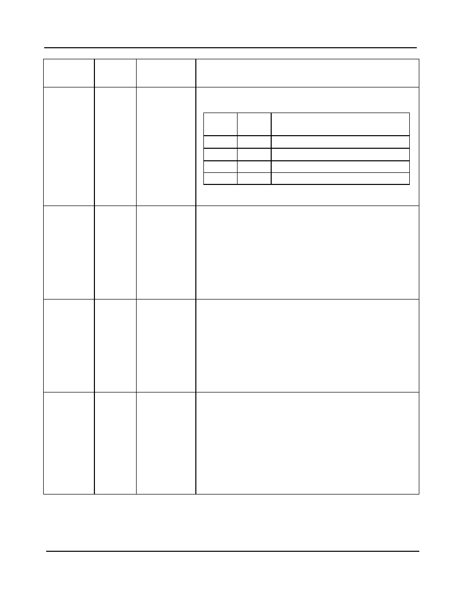
4.1 Input Clock (CKi) and Input Frame Pulse (FPi) Timing
The frequency of the input clock (CKi) for the ZL50017 must be at least twice the input/output data rate. For
example, if the input/output data rate is 8.192 Mbps, the input clock, CKi, must be 16.384 MHz. Following the
example above, if the input/output data rate is 4.096 Mbps, the input clock, CKi, must be 8.192 MHz.The only
exception to this is for 16.384 Mbps input/output data. In this case, the input clock, CKi, is equal to the data rate.
The input frame pulse, FPi, must always follow CKi. CKIN1 - 0 (bits 6 - 5) in the Control Register (CR) are used to
program the width of the input frame pulse and the frequency of the input clock supplied to the device.
The ZL50017 accepts positive and negative ST-BUS/GCI-Bus input clock and input frame pulse formats via the
programming of CKINP (bit 8) and FPINP (bit 7) in the Control Register (CR). By default, the device accepts the
negative input clock format and ST-BUS format frame pulses. However, the switch can also accept a positive-going
clock format by programming CKINP (bit 8) in the Control Register (CR). A GCI-Bus format frame pulse can be
used by programming FPINPOS (bit 9) and FPINP (bit 7) in the Control Register (CR).
Figure 4 - Input Timing when CKIN1 - 0 bits = "10" in the CR
FPi (244 ns)
FPINP = 0
FPINPOS = 0
FPi (244 ns)
FPINP = 1
FPINPOS = 0
FPi (244 ns)
FPINP = 0
FPINPOS = 1
FPi (244 ns)
FPINP = 1
FPINPOS = 1
CKi
(4.096 MHz)
CKINP = 0
CKi
(4.096 MHz)
CKINP = 1
7
6
1
0
0
7
STi
(2.048 Mbps)
Channel 0
Channel 31
ST
-BUS
GCI
-
Bu
s

ZL50017
Data Sheet
16
Zarlink Semiconductor Inc.
Figure 5 - Input Timing when CKIN1 - 0 bits = "01" in the CR
Figure 6 - Input Timing when CKIN1 - 0 = "00" in the CR
FPi (122 ns)
FPINP = 0
FPINPOS = 0
FPi (122 ns)
FPINP = 1
FPINPOS = 0
FPi (122 ns)
FPINP = 0
FPINPOS = 1
FPi (122 ns)
FPINP = 1
FPINPOS = 1
CKi
(8.192 MHz)
CKINP = 0
CKi
(8.192 MHz)
CKINP = 1
STi
(4.096 Mbps)
Channel 0
Channel 63
6
5
4
1
0
2
7
6
7
1
0
ST
-BUS
GCI
-
Bu
s
FPi (61ns)
FPINP = 0
FPINPOS = 0
FPi (61ns)
FPINP = 1
FPINPOS = 0
FPi (61ns)
FPINP = 0
FPINPOS = 1
FPi (61ns)
FPINP = 1
FPINPOS = 1
CKi
(16.384 MHz)
CKINP = 0
CKi
(16.384 MHz)
CKINP = 1
STi
(8.192 Mbps)
Channel 0
Channel N = 127
6 5 4 3 2 1
3 2 1 0
5 4
7
6 5
7
1 0
STi
(16.384 Mbps)
Channel 0
Channel N = 255
6
7
4
5
2
3
0
1
6
7
4
5
2
3
2
3
0
1
6
7
4
5
2
3
6
7
4
5
2
3
0
1
2
3
0
1
ST
-BUS
GC
I
-
Bu
s

ZL50017
Data Sheet
17
Zarlink Semiconductor Inc.
4.2 ST-BUS and GCI-Bus Timing
The ZL50017 is capable of operating using either the ST-BUS or GCI-Bus standards. By default, the ZL50017 is
configured for ST-BUS input and output timing. To set the input timing to conform to the GCI-Bus standard,
FPINPOS (bit 9) and FPINP (bit 7) in the Control Register (CR) must be set.
5.0 Data Input Delay and Data Output Advancement
Various registers are provided to adjust the input delay and output advancement for each input and output data
stream. The input bit delay and output bit advancement can vary from 0 to 7 bits for each individual stream.
If input delay of less than a bit is desired, different sampling points can be used to handle the adjustments. The
sampling point can vary from 1/4 to 4/4 with a 1/4-bit increment for all input streams. By default, the sampling point
is set to the 3/4-bit location.
The fractional output bit advancement can vary from 0 to 3/4 bits, again with a 1/4 bit increment. By default, there is
0 output bit advancement.
Although input delay or output advancement features are available on streams which are operating in bi-directional
mode it is not recommended, as it can easily cause bus contention. If users require this function, special attention
must be given to the timing to ensure contention is minimized.

ZL50017
Data Sheet
18
Zarlink Semiconductor Inc.
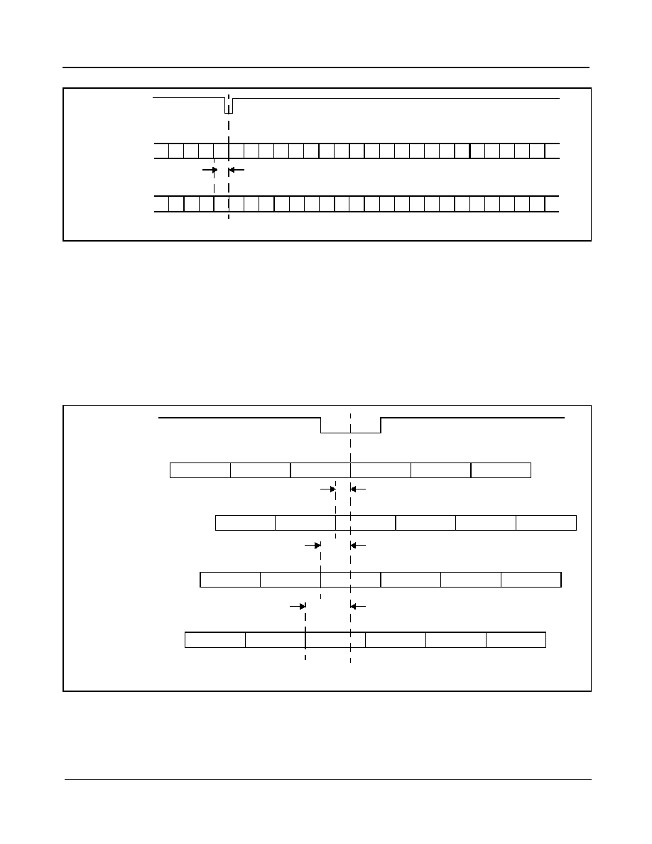
5.1 Input Bit Delay Programming
The input bit delay programming feature provides users with the flexibility of handling different wire delays when
designing with source streams for different devices.
By default, all input streams have zero bit delay, such that bit 7 is the first bit that appears after the input frame
boundary (assuming ST-BUS formatting). The input delay is enabled by STIN[n]BD2-0 (bits 8 - 6) in the Stream
Input Control Register 0 - 15 (SICR0 - 15) as described in Table 9 on page 32. The input bit delay can range from 0
to 7 bits.
Figure 7 - Input Bit Delay Timing Diagram (ST-BUS)
FPi
STi[n]
Bit Delay = 0
(Default)
Channel 0
7
Channel 1
6 5 4 3 2 1 0 7 6 5 4 3 2 1 0 7 6 5 4 3 2
Channel 2
2 1 0
4 3
Last Channel
STi[n]
Bit Delay = 1
Channel 0
7
Channel 1
6 5 4 3 2 1 0 7 6 5 4 3 2 1 0 7 6 5 4 3
Channel 2
2 1 0
4 3
Last Channel
Bit Delay = 1
5
Note: Last Channel = 31, 63, 127 and 255 for 2.048, 4.096, 8.192 and 16.384 Mbps modes respectively.

ZL50017
Data Sheet
19
Zarlink Semiconductor Inc.
5.2 Input Bit Sampling Point Programming
In addition to the input bit delay feature, the ZL50017 allows users to change the sampling point of the input bit by
programming STIN[n]SMP 1-0 (bits 5 - 4) in the Stream Input Control Register 0 - 15 (SICR0 - 15). For input
streams the default sampling point is at 3/4 bit and users can change the sampling point to 1/4, 1/2, 3/4 or 4/4 bit
position.
Figure 8 - Input Bit Sampling Point Programming
FPi
STi[n]
STIN[n]SMP1-0 = 01
(2, 4 or 8 Mbps)
Channel 0
Last Channel
Sampling Point = 1/4 Bit
STi[n]
STIN[n]SMP1-0 = 10
2, 4 or 8 Mbps
STIN[n]SMP1-0 = 00
16 Mbps - Default
Channel 0
Last Channel
Sampling Point = 1/2 Bit
STi[n]
STIN[n]SMP1-0 = 00
2, 4 or 8 Mbps - Default
Channel 0
Last Channel
Sampling Point = 3/4 Bit
1
0
7
6
2
Note: Last Channel = 31, 63, 127 and 255 for 2.048, 4.096, 8.192 and 16.384 Mbps mode respectively
STi[n]
STIN[n]SMP1-0 = 11
2, 4 or 8 Mbps
STIN[n]SMP1-0 = 10
16 Mbps
Channel 0
Last Channel
Sampling Point = 4/4 Bit
5
1
0
7
6
5
1
0
7
6
5
1
0
7
6
2
5

ZL50017
Data Sheet
20
Zarlink Semiconductor Inc.
The input delay is controlled by STIN[n]BD2-0 (bits 8 - 6) to control the bit shift and STIN[n]SMP1 - 0 (bits 5 - 4) to
control the sampling point in the Stream Input Control Register 0 - 15 (SICR0 - 15).
Figure 9 - Input Bit Delay and Factional Sampling Point
5.3 Output Advancement Programming
This feature is used to advance the output data of individual output streams with respect to the input frame
boundary. Each output stream has its own bit advancement value which can be programmed in the Stream Output
Control Register 0 - 15 (SOCR0 - 15).
By default, all output streams have zero bit advancement such that bit 7 is the first bit that appears after the input
frame boundary (assuming ST-BUS formatting). The output advancement is enabled by STO[n]AD 2 - 0 (bits 6 - 4)
of the Stream Output Control Register 0 - 15 (SOCR0 - 15) as described in Table 10 on page 33. The output bit
advancement can vary from 0 to 7 bits.
Nominal Channel n+1 Boundary
7
6
5
4
3
2
1
0
7
0
000 01
000 10
000 00 (Default)
000 11
001 01
001 10
001 00
001 11
010 01
010 10
010 00
010 11
011 01
011 10
011 00
011 11
111 00
111 10
111 01
110 11
110 00
110 10
110 01
101 11
101 00
101 10
101 01
100 11
100 00
100 10
100 01
111 11
The first 3 bits represent STIN[n]BD2 - 0 for setting the bit delay.
The second set of 2 bits represent STIN[n]SMP1 - 0 for setting the sampling point offset.
STi[n]
Nominal Channel n Boundary
Example: With a setting of 011 10 the offset will be 3 bits at a 1/2 sampling point.
Note: Italic settings can be used in 16 Mbps mode (1/2 and 4/4 sampling point).
ZL50017
Data Sheet
21
Zarlink Semiconductor Inc.
Figure 10 - Output Bit Advancement Timing Diagram (ST-BUS)
5.4 Fractional Output Bit Advancement Programming
In addition to the output bit advancement, the device has a fractional output bit advancement feature that offers
better resolution. The fractional output bit advancement is useful in compensating for varying parasitic load on the
serial data output pins.
By default all of the streams have zero fractional bit advancement such that bit 7 is the first bit that appears after the
output frame boundary. The fractional output bit advancement is enabled by STO[n]FA 1 - 0 (bits 8 - 7) in the
Stream Output Control Register 0 - 15 (SOCR0 - 15). For all streams the fractional bit advancement can vary from
0, 1/4, 1/2 to 3/4 bits.
Figure 11 - Output Fractional Bit Advancement Timing Diagram (ST-BUS)
FPi
STio[n]
Bit Adv = 0
(Default)
Channel 0
7
Channel 1
6 5 4 3 2 1 0 7 6 5 4 3 2 1 0 7 6 5 4 3 2
Channel 2
2 1 0
4 3
Last Channel
STio[n]
Bit Adv = 1
Channel 0
7
Channel 1
6 5 4 3 2 1 0 7 6 5 4 3 2 1 0 7 6 5 4 3
Channel 2
2 1 0
3
Last Channel
Bit Advancement = 1
Note: Last Channel = 31, 63, 127 and 255 for 2.048, 4.096, 8.192 and 16.384 Mbps modes respectively.
2 1
FPi
STio[n]
STo[n]FA1-0 = 00
(Default)
Channel 0
7
Last Channel
STio[n]
STo[n]FA1-0 = 01
(2, 4 or 8 Mbps)
Channel 0
Last Channel
Fractional Bit Advancement = 1/4 Bit
6
5
2
1
0
STio[n]
STo[n]FA1-0 = 10
(2, 4 or 8 Mbpa)
STo[n]FA1-0 = 01
(16Mbps)
Channel 0
Last Channel
Fractional Bit Advancement = 1/2 Bit
STio[n]
STo[n]FA1-0 = 11
(2, 4 or 8 Mbps)
Channel 0
Last Channel
Fractional Bit Advancement = 3/4 Bit
Note: Last Channel = 31, 63, 127 and 255 for 2.048, 4.096, 8.192 and 16.384 Mbps modes respectively.
7
6
5
1
0
7
6
5
1
0
7
6
5
1
0
4
4
4

ZL50017
Data Sheet
22
Zarlink Semiconductor Inc.
6.0 Data Delay Through the Switching Paths
The switching of information from the input serial streams to the output serial streams results in a throughput delay.
The device can be programmed to perform timeslot interchange functions with different throughput delay
capabilities on a per-channel basis. For voice applications, select variable throughput delay to ensure minimum
delay between input and output data. In wideband data applications, select constant delay to maintain the frame
integrity of the information through the switch. The delay through the device varies according to the type of
throughput delay selected by the V/C (bit 14) in the Connection Memory Low when CMM = 0.
6.1 Variable Delay Mode
Variable delay mode causes the output channel to be transmitted as soon as possible. This is a useful mode for
voice applications where the minimum throughput delay is more important than frame integrity. The delay through
the switch can vary from 7 channels to 1 frame + 7 channels. To set the device into variable delay mode, VAREN
(bit 4) in the Control Register (CR) must be set before V/C (bit 14) in the Connection Memory Low when CMM = 0.
If the VAREN bit is not set and the device is programmed for variable delay mode, the information read on the
output stream will not be valid.
In variable delay mode, the delay depends on the combination of the source and destination channels of the input
and output streams.
For example, if Stream 4 Channel 2 is switched to Stream 5 Channel 9 with variable delay, the data will be output in
the same 125
µs frame. Contrarily, if Stream 6 Channel 1 is switched to Stream 9 Channel 3, the information will
appear in the following frame.
Figure 12 - Data Throughput Delay for Variable Delay
m = input channel number
n = output channel number
n-m <= 0
0 < n-m < 7
n-m = 7
n-m > 7
STio < STi
STio >= STi
T = Delay between input and output
1 frame - (m-n)
1 frame + (n-m)
n-m
Table 1 - Delay for Variable Delay Mode
L-2
L-1 CH0 CH1 CH2 CH3
L-2
L-1 CH0 CH1 CH2 CH3
L-2
L-1 CH0 CH1 CH2 CH3
L-2
L-1 CH0 CH1 CH2 CH3
L-2
L-1 CH0 CH1 CH2 CH3
L-2
L-1 CH0 CH1 CH2 CH3
L-2
L-1 CH0 CH1 CH2 CH3
L-2
L-1 CH0 CH1 CH2 CH3
CH4 CH5 CH6
CH4 CH5 CH6
CH4 CH5 CH6
CH4 CH5 CH6
CH7 CH8 CH9
CH7 CH8 CH9
CH7 CH8 CH9
CH7 CH8 CH9
STi4
CH2
STio5
CH9
STi6
CH1
STio9
CH3
Frame N
Frame N + 1
L = last channel = 31, 63, 127 or 255 for 2.048 Mbps, 4.096 Mbps, 8.192 Mbps and 16.384 Mbps respectively.

ZL50017
Data Sheet
23
Zarlink Semiconductor Inc.
6.2 Constant Delay Mode
In this mode, frame integrity is maintained in all switching configurations. The delay though the switch is 2 frames -
Input Channel + Output Channel. This can result in a minimum of 1 frame + 1 channel delay if the last channel on a
stream is switched to the first channel of a stream. The maximum delay is 3 frames - 1 channel. This occurs when
the first channel of a stream is switched to the last channel of a stream. The constant delay mode is available for all
output channels.
The data throughput delay is expressed as a function of ST-BUS/GCI-Bus frames, input channel number (m) and
output channel number (n). The data throughput delay (T) is:
T = 2 frames + (n - m)
The constant delay mode is controlled by V/C (bit 14) in the Connection Memory Low when CMM = 0. When this bit
is set low, the channel is in constant delay mode. If VAREN (bit 4) in the Control Register (CR) is set (to enable
variable throughput delay on a chip-wide basis), the device can still be programmed to operate in constant delay
mode.
Figure 13 - Data Throughput Delay for Constant Delay
7.0 Connection Memory Description
The connection memory consists of two blocks, Connection Memory Low (CM_L). The CM_L is 16 bits wide and is
used for channel switching and other special modes. Each connection memory location of the CM_L or CM_H can
be read or written via the 16 bit microprocessor port within one microprocessor access cycle. See Table 11 on
page 34 for the address mapping of the connection memory. Any unused bits will be reset to zero on the 16-bit data
bus.
For the normal channel switching operation, CMM (bit 0) of the Connection Memory Low (CM_L) is programmed
low. SCA7 - 0 (bits 8 - 1) indicate the source (input) channel address and SSA4 - 0 (bits 13 - 9) indicate the source
(input) stream address. When CMM (bit 0) of the Connection Memory Low (CM_L) is programmed high, the
ZL50017 will operate in one of the special modes described in Table 13 on page 36. When the per-channel
message mode is enabled, MSG7 - 0 (bit 10 - 3) in the Connection Memory Low (CM_L) will be output via the serial
data stream as message output data.
L-2
L-1 CH0 CH1 CH2 CH3
L-2
L-1 CH0 CH1 CH2 CH3
L-2
L-1 CH0 CH1 CH2 CH3
L-2
L-1 CH0 CH1 CH2 CH3
L-2
L-1 CH0 CH1 CH2 CH3
L-2
L-1 CH0 CH1 CH2 CH3
L-2
L-1 CH0 CH1 CH2 CH3
L-2
L-1 CH0 CH1 CH2 CH3
L-2
L-1 CH0 CH1 CH2 CH3
L-2
L-1 CH0 CH1 CH2 CH3
L-2
L-1 CH0 CH1 CH2 CH3
L-2
L-1 CH0 CH1 CH2 CH3
STi
STio
STi
STio
L = last channel = 31, 63, 127 or 255 for 2.048 Mbps, 4.096 Mbps, 8.192 Mbps and 16.384 Mbps respectively.
Frame N
Frame N + 1
Frame N + 2

ZL50017
Data Sheet
24
Zarlink Semiconductor Inc.
8.0 Connection Memory Block Programming
This feature allows for fast initialization of the connection memory after power up.
8.1 Memory Block Programming Procedure
1. Set MBPE (bit 3) in the Control Register (CR) from low to high.
2. Configure BPD2 - 0 (bits 3 - 1) in the Internal Mode Selection (IMS) register to the desired values to be loaded
into CM_L.
3. Start the block programming by setting MBPS (bit 0) in the Internal Mode Selection Register (IMS) high. The val-
ues stored in BPD2 - 0 will be loaded into bits 2 - 0 of all CM_L positions. The remaining CM_L locations (bits 15
- 3).
The following tables show the resulting values that are in the CM_L and CM_H connection memory locations.
It takes at least two frame periods (250
µs) to complete a block program cycle.
MBPS (bit 0) in the Control Register (CR) will automatically reset to a low position after the block programming
process has completed.
MBPE (bit 3) in the Internal Mode Selection (IMS) register must be cleared from high to low to terminate the block
programming process. This is not an automatic action taken by the device and must be performed manually.
Note: Once the block program has been initiated, it can be terminated at any time prior to completion by setting
MBPS (bit 0) in the Control Register (CR) or MBPE (bit 3) in the Internal Mode Selection (IMS) register to low.
9.0 Microprocessor Port
The device provides access to the internal registers, connection memories and data memories via the
microprocessor port. The microprocessor port is capable of supporting both Motorola and Intel non-multiplexed
microprocessors. The microprocessor port consists of a 16-bit parallel data bus (D15 - 0), 14 bit address bus (A13 -
0) and six control signals (MOT_INTEL, CS, DS_RD, R/W_WR and DTA_RDY).
The data memory can only be read from the microprocessor port. For a data memory read operation, D7 - 0 will be
used and D15 - 8 will output zeros.
For a CM_L read or write operation, all bits (D15 - 0) of the data bus will be used. For a CM_H write operation, D4 -
0 of the data bus must be configured and D15 - 5 are ignored. D15 - 5 must be driven either high or low. For a
CM_H read operation, D4 - 0 will be used and D15 - 5 will output zeros.
Refer to Figure 15 on page 39, Figure 16 on page 40, Figure 17 on page 41 and Figure 18 on page 42 for the
microprocessor timing.
Bit
15
14
13
12
11
10
9
8
7
6
5
4
3
2
1
0
Value
0
0
0
0
0
0
0
0
0
0
0
0
0
BPD2
BPD1
BPD0
Table 2 - Connection Memory Low After Block Programming

ZL50017
Data Sheet
25
Zarlink Semiconductor Inc.
10.0 Device Reset and Initialization
The RESET pin is used to reset the ZL50017. When this pin is low, the following functions are performed:
Ј synchronously puts the microprocessor port in a reset state
Ј tristates the STio0 - 15 outputs
Ј preloads all internal registers with their default values (refer to the individual registers for default values)
Ј clears all internal counters
10.1 Power-up Sequence
The recommended power-up sequence is for the V
DD_IO
supply (normally +3.3 V) to be established before the
power-up of the V
DD_CORE
supply (normally +1.8 V). The V
DD_CORE
supply may be powered up at the same time
as V
DD_IO
, but should not "lead" the V
DD_IO
supply by more than 0.3 V.
10.2 Device Initialization on Reset
Upon power up, the ZL50017 should be initialized as follows:
Ј Set the ODE pin to low to disable the STio0 - 15 outputs
Ј Set the TRST pin to low to disable the JTAG TAP controller
Ј Reset the device by pulsing the RESET pin to zero for longer than 1
µs
Ј After releasing the RESET pin from low to high, wait for a certain period of time (see Note below) for the
device to stabilize from the power down state before the first microprocessor port access can occur
Ј Wait at least 500
µs prior to the next microport access (see Note below)
Ј Use the block programming mode to initialize the connection memory
Ј Release the ODE pin from low to high after the connection memory is programmed
Note: If CKi is 16.384 MHz, the waiting time is 500
µs; if CKi is 8.192 MHz, the waiting time is 1 ms; if CKi is
4.096 MHz, the waiting time is 2 ms.
10.3 Software Reset
In addition to the hardware reset from the RESET pin, the device can also be reset by using software reset
SRSTSW (bit 1) in the Software Reset Register (SRR).
11.0 JTAG Port
The JTAG test port is implemented to meet the mandatory requirements of the IEEE-1149.1 (JTAG) standard. The
operation of the boundary-scan circuitry is controlled by an external Test Access Port (TAP) Controller.
11.1 Test Access Port (TAP)
The Test Access Port (TAP) accesses the ZL50017 test functions. It consists of three input pins and one output pin
as follows:
Ј Test Clock Input (TCK) - TCK provides the clock for the test logic. TCK does not interfere with any on-chip
clock and thus remains independent in the functional mode. TCK permits shifting of test data into or out of
the Boundary-Scan register cells concurrently with the operation of the device and without interfering with
the on-chip logic.

ZL50017
Data Sheet
26
Zarlink Semiconductor Inc.
Ј Test Mode Selection Inputs (TMS) - The TAP Controller uses the logic signals received at the TMS input to
control test operations. The TMS signals are sampled at the rising edge of the TCK pulse. This pin is
internally pulled to high when it is not driven from an external source.
Ј Test Data Input (TDi) - Serial input data applied to this port is fed either into the instruction register or into a
test data register, depending on the sequence previously applied to the TMS input. The registers are
described in a subsequent section. The received input data is sampled at the rising edge of the TCK pulse.
This pin is internally pulled to high when it is not driven from an external source.
Ј Test Data Output (TDo) - Depending on the sequence previously applied to the TMS input, the contents of
either the instruction register or test data register are serially shifted out towards TDo. The data from TDo is
clocked on the falling edge of the TCK pulses. When no data is shifted through the boundary scan cells, the
TDo driver is set to a high impedance state.
Ј Test Reset (TRST) - Resets the JTAG scan structure. This pin is internally pulled to high when it is not
driven from an external source.
11.2 Instruction Register
The ZL50017 uses the public instructions defined in the IEEE-1149.1 standard. The JTAG interface contains a
four-bit instruction register. Instructions are serially loaded into the instruction register from the TDi when the TAP
Controller is in its shifted-OR state. These instructions are subsequently decoded to achieve two basic functions: to
select the test data register that may operate while the instruction is current and to define the serial test data
register path that is used to shift data between TDi and TDo during data register scanning.
11.3 Test Data Registers
As specified in the IEEE-1149.1 standard, the ZL50017 JTAG interface contains three test data registers:
Ј The Boundary-Scan Register - The Boundary-Scan register consists of a series of boundary-scan cells
arranged to form a scan path around the boundary of the ZL50017 core logic.
Ј The Bypass Register - The Bypass register is a single stage shift register that provides a one-bit path from
TDi to TDo.
Ј The Device Identification Register - The JTAG device ID for the ZL50017 is 0C36114B
H
11.4 BSDL
A Boundary Scan Description Language (BSDL) file is available from Zarlink Semiconductor to aid in the use of the
IEEE-1149.1 test interface.
Version
<31:28>
0000
Part Number
<27:12>
1100 0011 0110
0001
Manufacturer ID
<11:1>
0001 0100 101
LSB
<0>
1

ZL50017
Data Sheet
27
Zarlink Semiconductor Inc.
12.0 Register Address Mapping
Address
A13 - A0
CPU
Access
Register
Name
Abbreviation
Reset By
0000
H
R/W
Control Register
CR
Switch/Hardware
0001
H
R/W
Internal Mode Selection Register
IMS
Switch/Hardware
0002
H
R/W
Software Reset Register
SRR
Hardware Only
0008
H
R/W
Data Rate Selection Register
DRSR
Switch/Hardware
0010
H
R Only
Internal Flag Register
IFR
Switch/Hardware
0100
H
-
010F
H
R/W
Stream Input Control Registers 0 - 15
SICR0 - 15
Switch/Hardware
0200
H
-
020F
H
R/W
Stream Output Control Registers 0 - 15
SOCR0 - 15
Switch/Hardware
Table 3 - Address Map for Registers (A13 = 0)

ZL50017
Data Sheet
28
Zarlink Semiconductor Inc.
13.0 Detailed Register Description
Bit
Name
Description
15 - 10
Unused
Reserved. In normal functional mode, these bits MUST be set to zero.
9
FPINPOS
Input Frame Pulse (FPi) Position
When this bit is low, FPi straddles frame boundary (as defined by ST-BUS).
When this bit is high, FPi starts from frame boundary (as defined by GCI-Bus)
8
CKINP
Clock Input (CKi) Polarity
When this bit is low, the CKi falling edge aligns with the frame boundary.
When this bit is high, the CKi rising edge aligns with the frame boundary.
7
FPINP
Frame Pulse Input (FPi) Polarity
When this bit is low, the input frame pulse FPi has the negative frame pulse format.
When this bit is high, the input frame pulse FPi has the positive frame pulse format.
6 - 5
CKIN1 - 0
Input Clock (CKi) and Frame Pulse (FPi) Selection
The MODE_4M0 and MODE_4M1 pins, as described in "Pin Description" on page 9,
should also be set to define the input clock mode.
4
VAREN
Variable Delay Mode Enable
When this bit is low, the variable delay mode is disabled on a device-wide basis.
When this bit is high, the variable delay mode is enabled on a device-wide basis.
3
MBPE
Memory Block Programming Enable
When this bit is high, the connection memory block programming mode is enabled to
program the connection memory. When it is low, the memory block programming mode is
disabled.
Table 4 - Control Register (CR) Bits
External Read/Write Address: 0000
H
Reset Value: 0000
H
15
14
13
12
11
10
9
8
7
6
5
4
3
2
1
0
0
0
0
0
0
0
FPIN
POS
CKINP
FPINP
CKIN
1
CKIN
0
VAR
EN
MBPE
OSB
MS1
MS0
CKIN1 - 0
FPi Active Period
CKi
00
61 ns
16.384 MHz
01
122 ns
8.192 MHz
10
244 ns
4.096 MHz
11
Reserved

ZL50017
Data Sheet
29
Zarlink Semiconductor Inc.
2
OSB
Output Stand By Bit:
This bit enables the STio0 - 1 serial outputs. The following table describes the HiZ control
of the serial data outputs:
Note: Unused output streams are tristated (STio = HiZ). Refer to SOCR0 - 15 (bit 2 - 0).
1 - 0
MS1 - 0
Memory Select Bits
These two bits are used to select connection memory low, connection high or data mem-
ory for access by CPU:
Bit
Name
Description
Table 4 - Control Register (CR) Bits (continued)
External Read/Write Address: 0000
H
Reset Value: 0000
H
15
14
13
12
11
10
9
8
7
6
5
4
3
2
1
0
0
0
0
0
0
0
FPIN
POS
CKINP
FPINP
CKIN
1
CKIN
0
VAR
EN
MBPE
OSB
MS1
MS0
RESET
Pin
SRSTSW
(in SRR)
ODE
Pin
OSB
Bit
STio0 - 15
0
X
X
X
HiZ
1
1
X
X
HiZ
1
0
0
X
HiZ
1
0
1
0
HiZ
1
0
1
1
Active
(Controlled by CM)
MS1 - 0
Memory Selection
00
Connection Memory Low Read/Write
01
Reserved
10
Data Memory Read
11
Reserved

ZL50017
Data Sheet
30
Zarlink Semiconductor Inc.
Bit
Name
Description
15 - 9
Unused
Reserved. In normal functional mode, these bits MUST be set to zero.
8
STIO_PD_
EN
STio Pull-down Enable
When this bit is low, the pull-down resistors on all STio pads will be disabled.
When this bit is high, the pull-down resistors on all STio pads will be enabled.
7
Unused
Reserved. In normal functional mode, these bits MUST be set to zero.
6
BDL
Bi-directional Control
5 - 4
Unused
Reserved. In normal functional mode, these bits MUST be set to zero.
3 - 1
BPD2 - 0
Block Programming Data
These bits refer to the value to be loaded into the connection memory, whenever the
memory block programming feature is activated. After the MBPE bit in the Control
Register is set to high and the MBPS bit in this register is set to high, the contents of
the bits BPD2 - 0 are loaded into bits 2 - 0 of the Connection Memory Low. Bits 15 - 3
of the Connection Memory Low.
0
MBPS
Memory Block Programming Start:
A zero to one transition of this bit starts the memory block programming function. The
MBPS and BPD2 - 0 bits in this register must be defined in the same write operation.
Once the MBPE bit in the Control Register is set to high, the device requires two
frames to complete the block programming. After the programming function has fin-
ished, the MBPS bit returns to low, indicating the operation is completed. When MBPS
is high, MBPS or MBPE can be set to low to abort the programming operation.
Whenever the microprocessor writes a one to the MBPS bit, the block programming
function is started. As long as this bit is high, the user must maintain the same logical
value to the other bits in this register to avoid any change in the device setting.
Table 5 - Internal Mode Selection Register (IMS) Bits
External Read/Write Address: 0001
H
Reset Value: 0000
H
15
14
13
12
11
10
9
8
7
6
5
4
3
2
1
0
0
0
0
0
0
0
0
STIO_
PD_EN
0
BDL
0
0
BPD
2
BPD
1
BPD
0
MBPS
BDL
STio0 - 15 Operation
0
normal operation:
STi0-15 are inputs
STio0-15 are outputs
1
bi-directional operation:
STi0-15 tied low internally
STio0-15 are bi-directional

ZL50017
Data Sheet
31
Zarlink Semiconductor Inc.
Bit
Name
Description
15 - 2
Unused
Reserved
In normal functional mode, these bits MUST be set to zero.
1
SRSTSW
Software Reset Bit for Switch
When this bit is low, switching blocks are in normal operation. When this bit is high,
switching blocks are in software reset state. Refer to Table 12, "Address Map for
Registers (A13 = 0)" on page 32 for details regarding which registers are affected.
0
Unused
Reserved
In normal functional mode, these bits MUST be set to zero.
Table 6 - Software Reset Register (SRR) Bits
Bit
Name
Description
15 - 4
Unused
Reserved
In normal functional mode, these bits MUST be set to zero.
3 - 0
DR3 - 0
Input/Output Data Rate Selection Bits: These bits set the data rate for both input
and output streams
Table 7 - Data Rate Selection Register
External Read/Write Address: 0002
H
Reset Value: 0000
H
15
14
13
12
11
10
9
8
7
6
5
4
3
2
1
0
0
0
0
0
0
0
0
0
0
0
0
0
0
0
SRST
SW
0
External Read/Write Address: 0008
H
Reset Value: 0000
H
15
14
13
12
11
10
9
8
7
6
5
4
3
2
1
0
0
0
0
0
0
0
0
0
0
0
0
0
DR3
DR2
DR1
DR0
DR3 - 0
STio0 - 15 Operation
0000
Reserved
0001
2.048 Mbps
0010
4.096 Mbps
0011
8.192 Mbps
0100
16.384 Mbps
0101 - 1111
Reserved

ZL50017
Data Sheet
32
Zarlink Semiconductor Inc.
Bit
Name
Description
15 - 1
Unused
Reserved
In normal functional mode, these bits are zero.
0
PERR
Program Error (Read Only)
This bit is set high when the total number of input/output channels is programmed to
be more than the maximum capacity of 1024, in which case the input/output channels
beyond the maximum capacity should be disabled.This bit will be cleared automati-
cally after the total number of active streams/channels is correctly programmed to be
1024 channels or below.
Table 8 - Internal Flag Register (IFR) Bits - Read Only
Bit
Name
Description
15 - 9
Unused
Reserved
In normal functional mode, these bits MUST be set to zero
.
8 - 6
STIN[n]BD2 - 0
Input Stream[n] Bit Delay Bits.
The binary value of these bits refers to the number of bits that the input stream
will be delayed relative to FPi. The maximum value is 7. Zero means no delay.
5 - 4
STIN[n]SMP1 - 0
Input Data Sampling Point Selection Bits
3 - 1
Unused
Reserved
In normal functional mode, these bits MUST be set to zero
.
Table 9 - Stream Input Control Register 0 - 15 (SICR0 - 15) Bits
External Read Address: 0010
H
Reset Value: 0000
H
15
14
13
12
11
10
9
8
7
6
5
4
3
2
1
0
0
0
0
0
0
0
0
0
0
0
0
0
0
0
0
PERR
External Read/Write Address: 0100
H
- 010F
H
Reset Value: 0000
H
15
14
13
12
11
10
9
8
7
6
5
4
3
2
1
0
0
0
0
0
0
0
0
STIN[n]
BD2
STIN[n]
BD1
STIN[n]
BD0
STIN[n]
SMP1
STIN[n]
SMP0
0
0
0
STIN[n]
EN
STIN[n]SMP1-0
Sampling Point
(2.048 Mbps, 4.096 Mbps,
8.192 Mbps streams)
Sampling Point
16.384 Mbps streams)
00
3/4 point
1/2 point
01
1/4 point
10
2/4 point
4/4 point
11
4/4 point

ZL50017
Data Sheet
33
Zarlink Semiconductor Inc.
0
STIN[n]EN
Input Stream Enable Bit
When this bit is high the input stream is enabled. When this bit is low the input
stream is ignored
Note: [n] denotes input stream from 0 -
15
.
Bit
Name
Description
15 - 9
Unused
Reserved
In normal functional mode, these bits MUST be set to zero.
8 - 7
STO[n]FA1 - 0
Output Stream[n] Fractional Advancement Bits
6 - 4
STO[n]AD2 - 0
Output Stream[n] Bit Advancement Selection Bits
The binary value of these bits refers to the number of bits that the output stream
is to be advanced relative to FPi. The maximum value is 7. Zero means no
advancement.
3 - 1
Unused
Reserved
In normal functional mode, these bits MUST be set to zero
.
0
STO[n]EN
Output Stream Enable Bit
When this bit is high the output stream is enabled. When this bit is low the
output stream is set to high impedance
Note: [n] denotes output stream from 0 -
15
.
Table 10 - Stream Output Control Register 0 - 15 (SOCR0 - 15) Bits
Bit
Name
Description
Table 9 - Stream Input Control Register 0 - 15 (SICR0 - 15) Bits (continued)
External Read/Write Address: 0100
H
- 010F
H
Reset Value: 0000
H
15
14
13
12
11
10
9
8
7
6
5
4
3
2
1
0
0
0
0
0
0
0
0
STIN[n]
BD2
STIN[n]
BD1
STIN[n]
BD0
STIN[n]
SMP1
STIN[n]
SMP0
0
0
0
STIN[n]
EN
External Read/Write Address: 0200
H
- 020F
H
Reset Value: 0000
H
15
14
13
12
11
10
9
8
7
6
5
4
3
2
1
0
0
0
0
0
0
0
0
STO[n]
FA1
STO[n]
FA0
STO[n]
AD2
STO[n]
AD1
STO[n]
AD0
0
0
0
STO[n]
EN
STO[n]FA1-0
Advancement
(2.048 Mbps, 4.096 Mbps,
8.192 Mbps streams)
Advancement
(16.384 Mbps streams)
00
0
0
01
1/4 bit
2/4
10
2/4 bit
Reserved
11
3/4 bit

ZL50017
Data Sheet
34
Zarlink Semiconductor Inc.
14.0 Memory
14.1 Memory Address Mappings
When A13 is high, the data or connection memory can be accessed by the microprocessor port. Bit 1 - 0 in the
Control Register determine the access to the data or connection memory (CM_L or CM_H).
MSB
(Note 1)
Stream Address
(St0 - 15)
Channel Address
(Ch0 - 255)
A13
A12
A11
A10
A9
A8
Stream [n]
A7
A6
A5
A4
A3
A2
A1
A0
Channel [n]
1
1
1
1
1
1
1
1
1
.
.
.
.
.
1
1
0
0
0
0
0
0
0
0
0
.
.
.
.
.
0
0
0
0
0
0
0
0
0
0
1
.
.
.
.
.
1
1
0
0
0
0
1
1
1
1
0
.
.
.
.
.
1
1
0
0
1
1
0
0
1
1
0
.
.
.
.
.
1
1
0
1
0
1
0
1
0
1
0
.
.
.
.
.
0
1
Stream 0
Stream 1
Stream 2
Stream 3
Stream 4
Stream 5
Stream 6
Stream 7
Stream 8
.
.
.
.
.
Stream 14
Stream 15
0
0
.
.
0
0
0
0
.
.
0
0
.
.
0
0
.
.
.
.
1
1
0
0
.
.
0
0
0
0
.
.
0
0
.
.
1
1
.
.
.
.
1
1
0
0
.
.
0
0
1
1
.
.
1
1
.
.
1
1
.
.
.
.
1
1
0
0
.
.
1
1
0
0
1
1
.
.
1
1
.
.
.
.
1
1
0
0
.
.
1
1
0
0
.
.
1
1
.
.
1
1
.
.
.
.
1
1
0
0
.
.
1
1
0
0
.
1
1
.
.
1
1
.
.
.
.
1
1
0
0
.
.
1
1
0
0
1
1
.
.
1
1
.
.
.
.
1
1
0
1
.
.
0
1
0
1
.
.
0
1
.
.
0
1
.
.
.
.
0
1
Ch 0
Ch 1
.
.
Ch 30
Ch 31 (Note 2)
Ch 32
Ch 33
.
.
Ch 62
Ch 63 (Note 3)
.
.
Ch126
Ch 127 (Note 4)
.
.
.
.
Ch 254
Ch 255 (Note 5)
Notes:
1. A13 must be high for access to data and connection memory positions. A13 must be low to access internal registers.
2. Channels 0 to 31 are used when serial stream is at 2.048 Mbps.
3. Channels 0 to 63 are used when serial stream is at 4.096 Mbps.
4. Channels 0 to 127 are used when serial stream is at 8.192 Mbps.
5. Channels 0 to 255 are used when serial stream is at 16.384 Mbps.
Table 11 - Address Map for Memory Locations (A13 = 1)

ZL50017
Data Sheet
35
Zarlink Semiconductor Inc.
14.2 Connection Memory Low (CM_L) Bit Assignment
When the CMM bit (bit 0) in the connection memory low is zero, the per-channel transmission is set to the normal
channel-switching. The connection memory low bit assignment for the channel transmission mode is shown in
Table 12 on page 35.
Bit
Name
Description
15
Unused
Reserved
In normal functional mode, these bits MUST be set to zero.
14
V/C
Variable/Constant Delay Control
When this bit is low, the output data for this channel will be taken from con-
stant delay memory.
When this bit is set to high, the output data for this channel will be taken from
variable delay memory. Note that VAREN must be set in Control Register
first.
13
Unused
Reserved. In normal functional mode, this bit MUST be set to zero.
12 - 9
SSA3 - 0
Source Stream Address
The binary value of these 4 bits represents the input stream number.
8 - 1
SCA7 - 0
Source Channel Address
The binary value of these 8 bits represents the input channel number.
0
CMM = 0
Connection Memory Mode = 0
If this is low, the connection memory is in the normal switching mode. Bit 13 -
1 are the source stream number and channel number.
Table 12 - Connection Memory Low (CM_L) Bit Assignment when CMM = 0
15
14
13
12
11
10
9
8
7
6
5
4
3
2
1
0
0
V/C
0
SSA
3
SSA
2
SSA
1
SSA
0
SCA
7
SCA
6
SCA
5
SCA
4
SCA
3
SCA
2
SCA
1
SCA
0
CMM
=0

ZL50017
Data Sheet
36
Zarlink Semiconductor Inc.
When CMM is one, the device is programmed to perform one of the special per-channel transmission modes. Bits
PCC0 and PCC1 from connection memory are used to select the per-channel tristate or message mode as shown
in Table 13 on page 36.
Bit
Name
Description
15 - 11
Unused
Reserved
In normal functional mode, these bits MUST be set to zero.
10 - 3
MSG7 - 0
Message Data Bits
8-bit data for the message mode. Not used in the per-channel tristate.
2 - 1
PCC1 - 0
Per-Channel Control Bits
These two bits control the corresponding entry's value on the STio stream.
0
CMM = 1
Connection Memory Mode = 1
If this is high, the connection memory is in the per-channel control mode
which is per-channel tristate or per-channel message mode.
Table 13 - Connection Memory Low (CM_L) Bit Assignment when CMM = 1
15
14
13
12
11
10
9
8
7
6
5
4
3
2
1
0
0
0
0
0
0
MSG
7
MSG
6
MSG
5
MSG
4
MSG
3
MSG
2
MSG
1
MSG
0
PCC
1
PCC
0
CMM
=1
PC
C1
PC
C0
Channel Output Mode
0
0
Per Channel Tristate
0
1
Message Mode
1
0
Reserved
1
1
Reserved

ZL50017
Data Sheet
37
Zarlink Semiconductor Inc.
15.0 DC Parameters
* Exceeding these values may cause permanent damage. Functional operation under these conditions is not implied.
Typical figures are at 25
∞C and are for design aid only: not guaranteed and not subject to production testing.
Characteristics are over recommended operating conditions unless otherwise stated.
Typical figures are at 25∞C, VDD_CORE at 1.8 V and VDD_IO at 3.3 V and are for design aid only: not guaranteed and not subject to produc-
tion testing.
* Note 1: Maximum leakage on pins (output or I/O pins in high impedance state) is over an applied voltage (
V
IN
).
Absolute Maximum Ratings*
Parameter
Symbol
Min.
Max.
Units
1
I/O Supply Voltage
V
DD_IO
-0.5
5.0
V
2
Core Supply Voltage
V
DD_CORE
-0.5
2.5
V
3
Input Voltage
V
I_3V
-0.5
V
DD
+ 0.5
V
4
Input Voltage (5 V-tolerant inputs)
V
I_5V
-0.5
7.0
V
5
Continuous Current at Digital Outputs
I
o
15
mA
6
Package Power Dissipation
P
D
1.5
W
7
Storage Temperature
T
S
- 55
+125
∞C
Recommended Operating Conditions -
Voltages are with respect to ground (V
SS
) unless otherwise stated
.
Characteristics
Sym.
Min.
Typ.
Max.
Units
1
Operating Temperature
T
OP
-40
25
+85
∞C
2
Positive Supply
V
DD_IO
3.0
3.3
3.6
V
3
Positive Supply
V
DD_CORE
1.71
1.8
1.89
V
4
Input Voltage
V
I
0
3.3
V
DD_IO
V
5
Input Voltage on 5 V-Tolerant Inputs
V
I_5V
0
5.0
5.5
V
DC Electrical Characteristics
-
Voltages are with respect to ground (V
ss
) unless otherwise stated.
Characteristics
Sym.
Min.
Typ.
Max.
Units
Test Conditions
1
Supply Current - V
DD_CORE
I
DD_CORE
75
mA
2
Supply Current - V
DD_IO
I
DD_IO
40
mA
C
L
=30pF
3
Input High Voltage
V
IH
2.0
V
4
Input Low Voltage
V
IL
0.8
V
5
Input Leakage (input pins)
Input Leakage (bi-directional pins)
I
IL
I
BL
5
5
µA
µA
0
<V
IN
V
DD_IO
See Note 1
6
Weak Pullup Current
I
PU
-33
µA
Input at 0 V
7
Weak Pulldown Current
I
PD
33
µA
Input at V
DD_IO
8
Input Pin Capacitance
C
I
3
pF
9
Output High Voltage
V
OH
2.4
V
I
OH
= 8 mA
10 Output Low Voltage
V
OL
0.4
V
I
OL
= 8 mA
11 Output High Impedance Leakage
I
OZ
5
µA
0 < V < V
DD
12 Output Pin Capacitance
C
O
5
10
pF

ZL50017
Data Sheet
38
Zarlink Semiconductor Inc.
16.0 AC Parameters
Characteristics are over recommended operating conditions unless otherwise stated.
Figure 14 - Timing Parameter Measurement Voltage Levels
AC Electrical Characteristics
- Timing Parameter Measurement Voltage Levels
Characteristics
Sym.
Level
Units
Conditions
1
CMOS Threshold
V
CT
0.5 V
DD_IO
V
2
Rise/Fall Threshold Voltage High
V
HM
0.7 V
DD_IO
V
3
Rise/Fall Threshold Voltage Low
V
LM
0.3 V
DD_IO
V
Timing Reference Points
ALL SIGNALS
V
HM
V
CT
V
LM

ZL50017
Data Sheet
39
Zarlink Semiconductor Inc.
Characteristics are over recommended operating conditions unless otherwise stated.
Typical figures are at 25∞C, VDD_CORE at 1.8 V and VDD_IO at 3.3 V and are for design aid only: not guaranteed and not subject to produc-
tion testing.
Figure 15 - Motorola Non-Multiplexed Bus Timing - Read Access
AC Electrical Characteristics
- Motorola Non-Multiplexed Bus Mode - Read Access
Characteristics
Sym.
Min.
Typ.
Max.
Units
Test Conditions
2
1 CS de-asserted time
t
CSD
15
ns
2 DS de-asserted time
t
DSD
15
ns
3 CS setup to DS falling
t
CSS
0
ns
4 R/W setup to DS falling
t
RWS
10
ns
5 Address setup to DS falling
t
AS
5
ns
6 CS hold after DS rising
t
CSH
0
ns
7 R/W hold after DS rising
t
RWH
0
ns
8 Address hold after DS rising
t
AH
0
ns
9 Data setup to DTA Low
t
DS
8
ns
C
L
= 50 pF
10 Data Active to High Impedance
t
DHZ
8
ns
C
L
= 50 pF, R
L
= 1 K
(Note 1)
11 Acknowledgement delay time.
From DS low to DTA low:
Registers
Memory
t
AKD
75
185
ns
ns
C
L
= 50 pF
C
L
= 50 pF
12 Acknowledgement hold time.
From DS high to DTA high
t
AKH
4
12
ns
C
L
= 50 pF, R
L
= 1 K
(Note 1)
13 DTA drive high to HiZ
t
AKZ
8
ns
Note 1: High impedance is measured by pulling to the appropriate rail with R
L
, with timing corrected to cancel time taken to
discharge C
L
.
Note 2: A delay of 500
µs to 2 ms (see Section 10.2 on page 25) must be applied before the first microprocessor access is
performed after the RESET pin is set high.
DS
A0-A13
D0-D15
t
CSH
t
AH
t
RWS
R/W
t
AS
t
RWH
t
AKD
t
DS
t
AKH
DTA
V
CT
V
CT
V
CT
V
CT
V
CT
V
CT
VALID ADDRESS
VALID READ DATA
t
CSS
t
DSD
CS
t
AKZ
t
CSD
t
DHZ

ZL50017
Data Sheet
40
Zarlink Semiconductor Inc.
Characteristics are over recommended operating conditions unless otherwise stated.
Typical figures are at 25∞C, VDD_CORE at 1.8 V and VDD_IO at 3.3 V and are for design aid only: not guaranteed and not subject to produc-
tion testing.
Figure 16 - Motorola Non-Multiplexed Bus Timing - Write Access
AC Electrical Characteristics
- Motorola Non-Multiplexed Bus Mode - Write Access
Characteristics
Sym.
Min.
Typ.
Max.
Units
Test Conditions
2
1 CS de-asserted time
t
CSD
15
ns
2 DS de-asserted time
t
DSD
15
ns
3 CS setup to DS falling
t
CSS
0
ns
4 R/W setup to DS falling
t
RWS
10
ns
5 Address setup to DS falling
t
AS
5
ns
6 Data setup to DS falling
t
DS
0
ns
C
L
= 50 pF
7 CS hold after DS rising
t
CSH
0
ns
8 R/W hold after DS rising
t
RWH
0
ns
9 Address hold after DS rising
t
AH
0
ns
10 Data hold from DS rising
t
DH
5
ns
C
L
= 50 pF, R
L
= 1 K
(Note 1)
11 Acknowledgement delay time.
From DS low to DTA low:
Registers
Memory
t
AKD
55
150
ns
ns
C
L
= 50 pF
C
L
= 50 pF
12 Acknowledgement hold time.
From DS high to DTA high
t
AKH
4
12
ns
C
L
= 50 pF, R
L
= 1 K
(Note 1)
13 DTA drive high to HiZ
t
AKZ
8
ns
Note 1: High impedance is measured by pulling to the appropriate rail with R
L
, with timing corrected to cancel time taken to
discharge C
L
.
Note 2: A delay of 500
µs to 2 ms (see Section 10.2 on page 25) must be applied before the first microprocessor access is
performed after the RESET pin is set high.
DS
A0-A13
t
CSH
t
AH
t
RWS
R/W
t
AS
t
RWH
t
AKD
t
AKH
DTA
V
CT
V
CT
V
CT
V
CT
V
CT
t
CSS
t
DSD
CS
t
AKZ
D0-D15
t
DH
t
DS
V
CT
VALID WRITE DATA
t
CSD
VALID ADDRESS

ZL50017
Data Sheet
41
Zarlink Semiconductor Inc.
Characteristics are over recommended operating conditions unless otherwise stated.
Typical figures are at 25∞C, VDD_CORE at 1.8 V and VDD_IO at 3.3 V and are for design aid only: not guaranteed and not subject to produc-
tion testing.
Figure 17 - Intel Non-Multiplexed Bus Timing - Read Access
AC Electrical Characteristics
- Intel Non-Multiplexed Bus Mode - Read Access
Characteristics
Sym.
Min.
Typ.
Max.
Units
Test Conditions
2
1 CS de-asserted time
t
CSD
15
ns
2 RD setup to CS falling
t
RS
10
ns
3 WR setup to CS falling
t
WS
10
ns
4 Address setup to CS falling
t
AS
5
ns
5 RD hold after CS rising
t
RH
0
ns
6 WR hold after CS rising
t
WH
0
ns
7 Address hold after CS rising
t
AH
0
ns
8 Data setup to RDY high
t
DS
8
ns
C
L
= 50 pF
9 Data Active to High Impedance
t
CSZ
7
ns
C
L
= 50 pF, R
L
= 1 K
(Note 1)
10 Acknowledgement delay time.
From CS low to RDY high:
Registers
Memory
t
AKD
175
185
ns
ns
C
L
= 50 pF
C
L
= 50 pF
11 Acknowledgement hold time.
From CS high to RDY low
t
AKH
4
12
ns
C
L
= 50 pF, R
L
= 1 K
(Note 1)
12 RDY drive low to HiZ
t
AKZ
8
ns
Note 1: High impedance is measured by pulling to the appropriate rail with R
L
, with timing corrected to cancel time taken to
discharge C
L
.
Note 2: A delay of 500
µs to 2 ms (see Section 10.2 on page 25) must be applied before the first microprocessor access is
performed after the RESET pin is set high.
CS
A0-A13
D0-D15
t
AH
t
WS
WR
t
WH
t
AKD
t
DS
t
AKH
RDY
V
CT
V
CT
V
CT
V
CT
V
CT
VALID ADDRESS
VALID READ DATA
t
CSD
t
AKZ
t
RS
RD
t
RH
V
CT
t
AS
t
CSZ

ZL50017
Data Sheet
42
Zarlink Semiconductor Inc.
Characteristics are over recommended operating conditions unless otherwise stated.
Typical figures are at 25∞C, VDD_CORE at 1.8 V and VDD_IO at 3.3 V and are for design aid only: not guaranteed and not subject to produc-
tion testing.
Figure 18 - Intel Non-Multiplexed Bus Timing - Write Access
AC Electrical Characteristics
- Intel Non-Multiplexed Bus Mode - Write Access
Characteristics
Sym.
Min.
Typ.
Max.
Units
Test Conditions
2
1 CS de-asserted time
t
CSD
15
ns
2 WR setup to CS falling
t
WS
10
ns
3 RD setup to CS falling
t
RS
10
ns
4 Address setup to CS falling
t
AS
5
ns
5 Data setup to CS falling
t
DS
0
ns
C
L
= 50 pF
6 WR hold after CS rising
t
WH
0
ns
7 RD hold after CS rising
t
RH
0
ns
8 Address hold after CS rising
t
AH
10
ns
9 Data hold after CS rising
t
DH
5
ns
C
L
= 50 pF, R
L
= 1 K
(Note 1)
10 Acknowledgement delay time.
From CS low to RDY high:
Registers
Memory
t
AKD
55
150
ns
ns
C
L
= 50 pF
C
L
= 50 pF
11 Acknowledgement hold time.
From CS high to RDY low
t
AKH
4
12
ns
C
L
= 50 pF, R
L
= 1 K
(Note 1)
12 RDY drive low to HiZ
t
AKZ
8
ns
Note 1: High impedance is measured by pulling to the appropriate rail with R
L
, with timing corrected to cancel time taken to
discharge C
L
.
Note 2: A delay of 500
µs to 2 ms (Section 10.2 on page 25) must be applied before the first microprocessor access is performed
after the RESET pin is set high.
CS
A0-A13
D0-D15
t
AH
t
RS
RD
t
RH
t
AKD
t
AKH
RDY
V
CT
V
CT
V
CT
V
CT
V
CT
VALID ADDRESS
t
CSD
t
AKZ
t
WS
WR
t
WH
V
CT
t
AS
VALID WRITE DATA
t
DS
t
DH

ZL50017
Data Sheet
43
Zarlink Semiconductor Inc.
Characteristics are over recommended operating conditions unless otherwise stated.
Typical figures are at 25∞C, VDD_CORE at 1.8 V and VDD_IO at 3.3 V and are for design aid only: not guaranteed and not subject to produc-
tion testing.
Figure 19 - JTAG Test Port Timing Diagram
AC Electrical Characteristics
- JTAG Test Port Timing
Characteristic
Sym.
Min.
Typ.
Max.
Units
Notes
1
TCK Clock Period
t
TCKP
100
ns
2
TCK Clock Pulse Width High
t
TCKH
20
ns
3
TCK Clock Pulse Width Low
t
TCKL
20
ns
4
TMS Set-up Time
t
TMSS
10
ns
5
TMS Hold Time
t
TMSH
10
ns
6
TDi Input Set-up Time
t
TDIS
20
ns
7
TDi Input Hold Time
t
TDIH
60
ns
8
TDo Output Delay
t
TDOD
30
ns
C
L
= 30 pF
9
TRST pulse width
t
TRSTW
200
ns
t
TMSH
t
TMSS
t
TCKL
t
TCKH
t
TCKP
t
TDIS
t
TDIH
t
TDOD
t
TRSTW
TMS
TCK
TDi
TDo
TRST

ZL50017
Data Sheet
44
Zarlink Semiconductor Inc.
Characteristics are over recommended operating conditions unless otherwise stated.
Typical figures are at 25∞C, VDD_CORE at 1.8 V and VDD_IO at 3.3 V and are for design aid only: not guaranteed and not subject to produc-
tion testing.
Characteristics are over recommended operating conditions unless otherwise stated.
Typical figures are at 25∞C, VDD_CORE at 1.8 V and VDD_IO at 3.3 V and are for design aid only: not guaranteed and not subject to produc-
tion testing.
AC Electrical Characteristics
- FPi and CKi Timing when CKIN1-0 bits = 00 (16.384 MHz)
Characteristic
Sym.
Min.
Typ.
Max. Units Notes
1
FPi Input Frame Pulse Width
t
FPIW
40
61
115
ns
2
FPi Input Frame Pulse Setup Time
t
FPIS
20
ns
3
FPi Input Frame Pulse Hold Time
t
FPIH
20
ns
4
CKi Input Clock Period
t
CKIP
55
61
67
ns
5
CKi Input Clock High Time
t
CKIH
27
34
ns
6
CKi Input Clock Low Time
t
CKIL
27
34
ns
7
CKi Input Clock Rise/Fall Time
t
r
CKi, t
f
CKi
3
ns
8
CKi Input Clock Cycle to Cycle Variation
t
CVC
0
20
ns
AC Electrical Characteristics
- FPi and CKi Timing when CKIN1-0 bits = 01 (8.192 MHz)
Characteristic
Sym.
Min.
Typ.
Max. Units Notes
1
FPi Input Frame Pulse Width
t
FPIW
90
122
220
ns
2
FPi Input Frame Pulse Setup Time
t
FPIS
45
ns
3
FPi Input Frame Pulse Hold Time
t
FPIH
45
ns
4
CKi Input Clock Period
t
CKIP
110
122
135
ns
5
CKi Input Clock High Time
t
CKIH
55
69
ns
6
CKi Input Clock Low Time
t
CKIL
55
69
ns
7
CKi Input Clock Rise/Fall Time
t
r
CKi, t
f
CKi
3
ns
8
CKi Input Clock Cycle to Cycle Variation
t
CVC
0
20
ns

ZL50017
Data Sheet
45
Zarlink Semiconductor Inc.
Characteristics are over recommended operating conditions unless otherwise stated.
Typical figures are at 25∞C, VDD_CORE at 1.8 V and VDD_IO at 3.3 V and are for design aid only: not guaranteed and not subject to produc-
tion testing.
Figure 20 - Frame Pulse Input and Clock Input Timing Diagram (ST-BUS)
Figure 21 - Frame Pulse Input and Clock Input Timing Diagram (GCI-Bus)
AC Electrical Characteristics
- FPi and CKi Timing when CKIN1-0 bits = 10 (4.096 MHz)
Characteristic
Sym.
Min.
Typ.
Max. Units Notes
1
FPi Input Frame Pulse Width
t
FPIW
90
244
420
ns
2
FPi Input Frame Pulse Setup Time
t
FPIS
110
ns
3
FPi Input Frame Pulse Hold Time
t
FPIH
110
ns
4
CKi Input Clock Period
t
CKIP
220
244
270
ns
5
CKi Input Clock High Time
t
CKIH
110
135
ns
6
CKi Input Clock Low Time
t
CKIL
110
135
ns
7
CKi Input Clock Rise/Fall Time
t
r
CKi, t
f
CKi
3
ns
8
CKi Input Clock Cycle to Cycle Variation
t
CVC
0
20
ns
t
FPIW
FPi
t
FPIH
t
CKIH
t
CKIL
t
FPIS
t
CKIP
CKi
Input Frame Boundary
t
rCKI
t
fCKI
t
FPIW
FPi
t
FPIH
t
CKIH
t
CKIL
t
FPIS
t
CKIP
CKi
Input Frame Boundary
t
rCKI
t
fCKI

ZL50017
Data Sheet
46
Zarlink Semiconductor Inc.
Characteristics are over recommended operating conditions unless otherwise stated.
Typical figures are at 25∞C, VDD_CORE at 1.8 V and VDD_IO at 3.3 V and are for design aid only: not guaranteed and not subject to produc-
tion testing.
Note 1: High impedance is measured by pulling to the appropriate rail with R
L
, with timing corrected to cancel the time taken to
discharge C
L
.
AC Electrical Characteristics
- ST-BUS/GCI-Bus Input Timing
Characteristic
Sym.
Min.
Typ.
Max.
Units
Test Conditions
1 STi Setup Time
2.048 Mbps
4.096 Mbps
8.192 Mbps
16.384 Mbps
t
SIS2
t
SIS4
t
SIS8
t
SIS16
5
5
5
5
ns
ns
ns
ns
2 STi Hold Time
2.048 Mbps
4.096 Mbps
8.192 Mbps
16.384 Mbps
t
SIH2
t
SIH4
t
SIH8
t
SIH16
8
8
8
8
ns
ns
ns
ns
3 STio Delay - Active to Active
@2.048 Mbps
@4.096 Mbps
@8.192 Mbps
@16.384 Mbps
t
SOD2
t
SOD4
t
SOD8
t
SOD16
-6
-6
-6
-6
0
0
0
0
ns
ns
ns
ns
C
L
= 30 pF
4 STio Delay - Active to High-Z
STio Delay - High-Z to Active
2.048 Mbps
4.096 Mbps
8.192 Mbps
16.384 Mbps
t
DZ
t
ZD
-8
-8
-8
-8
0
0
0
0
ns
ns
ns
ns
R
L
= 1 k,
C
L
= 30 pF,
See Note 1.
5 Output Drive Enable (ODE)
Delay
- High-Z to
Active
t
ZD_OD
E
260
ns
6 Output Drive Enable (ODE)
Delay
- Active to High-Z
t
DZ_OD
E
260
ns

ZL50017
Data Sheet
47
Zarlink Semiconductor Inc.
Figure 22 - ST-BUS Input and Output Timing Diagram when Operated at 2, 4, 8 and 16 Mbps
V
TT
CKi
FPi
(16.384 MHz)
CKi
FPi
(8.192 MHz)
CKi
FPi
(4.096 MHz)
t
SIS2
t
SIH2
Bit7
Ch0
Bit6
Ch0
t
SIS4
t
SIH4
Bit7
Ch0
Bit6
Ch0
Bit5
Ch0
Bit4
Ch0
Bit0
Ch63
Bit7
Ch0
Bit6
Ch0
Bit5
Ch0
Bit4
Ch0
Bit3
Ch0
Bit2
Ch0
Bit1
Ch0
Bit0
Ch0
Bit1
Ch127
8.192 Mbps
4.096 Mbps
2.048 Mbps
t
SIS8
t
SIH8
STi0 - 15
STi0 - 15
STi0 - 15
V
CT
V
CT
Bit0
Ch31
V
CT
Input Frame Boundary
Bit0
Ch127
8.192 Mbps
4.096 Mbps
2.048 Mbps
STio0 - 15
STio0 - 15
STio0 - 15
Bit0
Ch0
Bit1
Ch0
Bit2
Ch0
Bit3
Ch0
Bit7
Ch63
Bit0
Ch0
Bit1
Ch0
Bit7
Ch31
t
SOD2
/t
DZ
/t
ZD
t
SOD4
/t
DZ
/t
ZD
t
SOD8
/t
DZ
/t
ZD
V
CT
V
CT
V
CT
Bit7
Ch127
Bit0
Ch0
Bit1
Ch0
Bit2
Ch0
Bit3
Ch0
Bit4
Ch0
Bit5
Ch0
Bit6
Ch0
Bit7
Ch0
Bit6
Ch127
Bit7
Ch255
Bit0
Ch0
Bit1
Ch0
Bit2
Ch0
Bit3
Ch0
Bit4
Ch0
Bit5
Ch255
Bit6
Ch255
Bit5
Ch0
Bit6
Ch0
Bit7
Ch0
Bit0
Ch1
Bit1
Ch1
Bit2
Ch1
Bit3
Ch1
Bit4
Ch1
Bit5
Ch1
V
CT
t
SOD16
/t
DZ
/t
ZD
16.384 Mbps
STio0 - 15

ZL50017
Data Sheet
48
Zarlink Semiconductor Inc.
Figure 23 - GCI-Bus Input and Output Timing Diagram when Operated at 2, 4, 8 and 16 Mbps
V
TT
CKi
FPi
(16.384 MHz)
CKi
FPi
(8.192 MHz)
CKi
FPi
(4.096 MHz)
t
SIS2
t
SIH2
Bit0
Ch0
Bit1
Ch0
t
SIS4
t
SIH4
Bit0
Ch0
Bit1
Ch0
Bit2
Ch0
Bit3
Ch0
Bit7
Ch63
Bit0
Ch0
Bit1
Ch0
Bit2
Ch0
Bit3
Ch0
Bit4
Ch0
Bit5
Ch0
Bit6
Ch0
Bit7
Ch0
Bit6
Ch127
8.192 Mbps
4.096 Mbps
2.048 Mbps
t
SIS8
t
SIH8
STi0 - 15
STi0 - 15
STi0 - 15
V
CT
V
CT
Bit7
Ch31
V
CT
Input Frame Boundary
Bit7
Ch127
8.192 Mbps
4.096 Mbps
2.048 Mbps
STio0 - 15
STio0 - 15
STio0 - 15
Bit0
Ch0
Bit1
Ch0
Bit2
Ch0
Bit3
Ch0
Bit7
Ch63
Bit0
Ch0
Bit1
Ch0
Bit7
Ch31
t
SOD2
t
SOD4
t
SOD8
V
CT
V
CT
V
CT
Bit7
Ch127
Bit0
Ch0
Bit1
Ch0
Bit2
Ch0
Bit3
Ch0
Bit4
Ch0
Bit5
Ch0
Bit6
Ch0
Bit7
Ch0
Bit6
Ch127
Bit7
Ch255
Bit0
Ch0
Bit1
Ch0
Bit2
Ch0
Bit3
Ch0
Bit4
Ch0
Bit5
Ch255
Bit6
Ch255
Bit5
Ch0
Bit6
Ch0
Bit7
Ch0
Bit0
Ch1
Bit1
Ch1
Bit2
Ch1
Bit3
Ch1
Bit4
Ch1
Bit5
Ch1
V
CT
t
SOD16
16.384 Mbps
STio0 - 15

c Zarlink Semiconductor 2003 All rights reserved.
APPRD.
ISSUE
DATE
ACN
Package Code
Previous package codes
b
214440
1
26June03

c Zarlink Semiconductor 2003 All rights reserved.
APPRD.
ISSUE
DATE
ACN
Package Code
Previous package codes

www.zarlink.com
Information relating to products and services furnished herein by Zarlink Semiconductor Inc. or its subsidiaries (collectively "Zarlink") is believed to be reliable.
However, Zarlink assumes no liability for errors that may appear in this publication, or for liability otherwise arising from the application or use of any such
information, product or service or for any infringement of patents or other intellectual property rights owned by third parties which may result from such application or
use. Neither the supply of such information or purchase of product or service conveys any license, either express or implied, under patents or other intellectual
property rights owned by Zarlink or licensed from third parties by Zarlink, whatsoever. Purchasers of products are also hereby notified that the use of product in
certain ways or in combination with Zarlink, or non-Zarlink furnished goods or services may infringe patents or other intellectual property rights owned by Zarlink.
This publication is issued to provide information only and (unless agreed by Zarlink in writing) may not be used, applied or reproduced for any purpose nor form part
of any order or contract nor to be regarded as a representation relating to the products or services concerned. The products, their specifications, services and other
information appearing in this publication are subject to change by Zarlink without notice. No warranty or guarantee express or implied is made regarding the
capability, performance or suitability of any product or service. Information concerning possible methods of use is provided as a guide only and does not constitute
any guarantee that such methods of use will be satisfactory in a specific piece of equipment. It is the user's responsibility to fully determine the performance and
suitability of any equipment using such information and to ensure that any publication or data used is up to date and has not been superseded. Manufacturing does
not necessarily include testing of all functions or parameters. These products are not suitable for use in any medical products whose failure to perform may result in
significant injury or death to the user. All products and materials are sold and services provided subject to Zarlink's conditions of sale which are available on request.
Purchase of Zarlink's I
2
C components conveys a licence under the Philips I
2
C Patent rights to use these components in and I
2
C System, provided that the system
conforms to the I
2
C Standard Specification as defined by Philips.
Zarlink, ZL and the Zarlink Semiconductor logo are trademarks of Zarlink Semiconductor Inc.
Copyright Zarlink Semiconductor Inc. All Rights Reserved.
TECHNICAL DOCUMENTATION - NOT FOR RESALE
For more information about all Zarlink products
visit our Web Site at