Document Outline
- Features
- Applications
- Device Overview
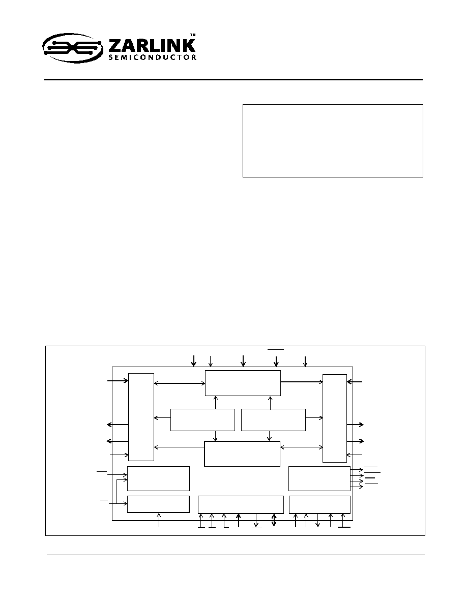
- Figure 1 - ZL50060/1 Functional Block Diagram
- Figure 2 - ZL50061 PBGA Connections (272 PBGA, 27 mm x 27 mm) Pin Diagram (as viewed through top of package)
- Figure 3 - ZL50060 PBGA Connections (256 PBGA, 17 mm x 17 mm) Pin Diagram (as viewed through top of package)
- Pin Description (continued)
- 1.0 Unidirectional and Bi-directional Switching Applications
- Figure 4 - 16,384 x 16,384 Channels (16 Mbps), Unidirectional Switching
- Figure 5 - 8,192 x 8,192 Channels (16 Mbps), Bi-directional Switching
- 1.1 Flexible Configuration
- 1.1.1 Non-Blocking Unidirectional Configuration (Typical System Configuration)
- 1.1.2 Non-Blocking Bi-directional Configuration
- 1.1.3 Blocking Bi-directional Configuration
- Figure 6 - 12,288 by 4,096 Channels Blocking Bi-directional Configuration
- 2.0 Functional Description
- 2.1 Switching Configuration
- 2.1.1 Unidirectional Switch
- 2.1.2 Backplane-to-Local Path
- 2.1.3 Local-to-Backplane Path
- 2.1.4 Backplane-to-Backplane Path
- 2.1.5 Local-to-Local Path
- 2.1.6 Port Data Rate Modes and Selection
- Table 1 - Per-stream Input and Output Data Rate Selection: Backplane and Local
- 2.1.7 Local Port Rate Selection
- 2.1.7.1 Local Input Port
- 2.1.7.2 Local Output Port
- 2.1.8 Backplane Port Rate Selection
- 2.1.8.1 Backplane Input Port
- 2.1.8.2 Backplane Output Port
- 2.2 Frame Pulse Input and Master Input Clock Timing
- Figure 7 - ST-BUS and GCI-Bus Input Timing Diagram for Different Data Rates
- 2.3 Input Frame Pulse and Generated Frame Pulse Alignment
- Figure 8 - Input and Output Frame Pulse Alignment for Different Data Rates
- 2.4 Jitter Tolerance Improvement Circuit - Frame Boundary Discriminator
- 2.5 Input Clock Jitter Tolerance
- 2.6 Backward Compatibility with MT90869
- 3.0 Input and Output Offset Programming
- 3.1 Input Offsets
- 3.1.1 Input Channel Delay Programming (Backplane and Local Input Streams)
- Figure 9 - Backplane and Local Input Channel Delay Timing Diagram (assuming 8 Mbps operation)
- 3.1.2 Input Bit Delay Programming (Backplane and Local Input Streams)
- Figure 10 - Backplane and Local Input Bit Delay Timing Diagram for Data Rate of 16 Mbps
- Figure 11 - Backplane and Local Input Bit Delay or Sampling Point Selection Timing Diagram for Data Rate of 8 Mbps
- 3.2 Output Advancement Programming (Backplane and Local Output Streams)
- Figure 12 - Local and Backplane Output Advancement Timing Diagram for Data Rate of 16 Mbps
- 4.0 Port high impedance Control
- Table 2 - Local and Backplane Output Enable Control Priority
- 4.1 LORS/BORS Asserted LOW, Non-32Mbps Mode
- Table 3 - L/BCSTo Allocation of Channel Control Bits to Output Streams (Non-32 Mbps Mode)
- Figure 13 - Local/Backplane Port External High Impedance Control Timing (Non-32 Mbps Mode)
- 4.2 LORS/BORS Asserted LOW, 32Mbps Mode
- Table 4 - L/BCSTo Allocation of Channel Control Bits to Output Streams (32 Mbps Mode)
- Figure 14 - Local and Backplane Port External High Impedance Control Timing (32Mbps Mode)
- 4.3 LORS/BORS Asserted HIGH
- 5.0 Data Delay Through the Switching Paths
- Table 5 - Variable Range for Input Streams
- Table 6 - Variable Range for Output Streams
- Table 7 - Data Throughput Delay
- Figure 15 - Data Throughput Delay with Input Channel Delay Disabled, Input Ch0 Switched to Output Ch0
- Figure 16 - Data Throughput Delay with Input Channel Delay Disabled, Input Ch0 Switched to Output Ch13
- Figure 17 - Data Throughput Delay with Input Channel Delay Disabled, Input Ch13 Switched to Output Ch0
- Figure 18 - Data Throughput Delay with Input Channel Delay Enabled, Input Ch0 Switched to Output Ch0
- Figure 19 - Data Throughput Delay with Input Channel Delay Enabled, Input Ch0 Switched to Output Ch13
- Figure 20 - Data Throughput Delay with Input Channel Delay Enabled, Input Ch13 Switched to Output Ch0
- 6.0 Bit Error Rate Test
- Figure 21 - Examples of BER Transmission Channels on a 16Mbps Output Stream
- 7.0 Microprocessor Port
- 8.0 Device Power-up, Initialization and Reset
- 8.1 Power-Up Sequence
- 8.2 Initialization
- 8.3 Reset
- Figure 22 - Hardware RESET de-assertion
- 9.0 Connection Memory
- 9.1 Local Connection Memory
- 9.2 Backplane Connection Memory
- Table 8 - Local and Backplane Connection Memory Configuration
- 9.3 Connection Memory Block Programming
- 9.3.1 Memory Block Programming Procedure:
- Table 9 - Local Connection Memory in Block Programming Mode
- Table 10 - Backplane Connection Memory in Block Programming Mode
- 10.0 Memory Built-In-Self-Test (BIST) Mode
- 11.0 JTAG Port
- 11.1 Test Access Port (TAP)
- 11.2 TAP Registers
- 11.2.1 Test Instruction Register
- 11.2.2 Test Data Registers
- 11.2.2.3 The Device Identification Register
- 11.3 Boundary Scan Description Language (BSDL) File
- 12.0 Memory Address Mappings
- Table 11 - Address Map for Data and Connection Memory Locations (A14 = 1)
- 12.1 Local Data Memory Bit Definition
- Table 12 - Local Data Memory (LDM) Bits
- 12.2 Backplane Data Memory Bit Definition
- Table 13 - Backplane Data Memory (BDM) Bits
- 12.3 Local Connection Memory Bit Definition
- Table 14 - LCM Bits for Non-32Mbps Source-to-Local Switching
- Table 15 - LCM Bits for 32Mbps Source-to-Local Switching
- 12.4 Backplane Connection Memory Bit Definition
- Table 16 - BCM Bits for Non-32Mbps Source-to-Backplane Switching
- Table 17 - BCM Bits for 32Mbps Source-to-Backplane Switching
- 13.0 Internal Register Mappings
- Table 18 - Address Map for Registers (A14 = 0)
- 14.0 Detailed Register Descriptions
- 14.1 Control Register (CR)
- Table 19 - Control Register Bits
- Figure 23 - Frame Boundary Conditions, ST-BUS Operation
- Figure 24 - Frame Boundary Conditions, GCI-Bus Operation
- 14.2 Block Programming Register (BPR)
- Table 20 - Block Programming Register Bits
- 14.3 Bit Error Rate Test Control Register (BERCR)
- Table 21 - Bit Error Rate Test Control Register (BERCR) Bits
- 14.4 Local Input Channel Delay Registers (LCDR0 to LCDR31)
- Table 22 - Local Input Channel Delay Register (LCDRn) Bits
- 14.4.1 Local Channel Delay Bits 8-0 (LCD8 - LCD0)
- Table 23 - Local Input Channel Delay (LCD) Programming Table
- 14.5 Local Input Bit Delay Registers (LIDR0 to LIDR31)
- Table 24 - Local Input Bit Delay Register (LIDRn) Bits
- 14.5.1 Local Input Delay Bits 4-0 (LID[4:0])
- Table 25 - Local Input Bit Delay and Sampling Point Programming Table
- 14.6 Backplane Input Channel Delay Registers (BCDR0 to BCDR31)
- Table 26 - Backplane Input Channel Delay Register (BCDRn) Bits
- 14.6.1 Backplane Channel Delay Bits 8-0 (BCD8 - BCD0)
- Table 27 - Backplane Input Channel Delay (BCD) Programming Table
- 14.7 Backplane Input Bit Delay Registers (BIDR0 to BIDR31)
- Table 28 - Backplane Input Bit Delay Register (BIDRn) Bits
- 14.7.1 Backplane Input Delay Bits 4-0 (BID[4:0])
- Table 29 - Backplane Input Bit Delay and Sampling Point Programming Table
- 14.8 Local Output Advancement Registers (LOAR0 to LOAR31)
- Table 30 - Local Output Advancement Register (LOAR) Bits
- 14.8.1 Local Output Advancement Bits 1-0 (LOA1-LOA0)
- Table 31 - Local Output Advancement (LOAR) Programming Table
- 14.9 Backplane Output Advancement Registers (BOAR0 - BOAR31)
- Table 32 - Backplane Output Advancement Register (BOAR) Bits
- 14.9.1 Backplane Output Advancement Bits 1-0 (BOA1-BOA0)
- Table 33 - Backplane Output Advancement (BOAR) Programming Table
- 14.10 Local Bit Error Rate (BER) Registers
- 14.10.1 Local BER Start Send Register (LBSSR)
- Table 34 - Local BER Start Send Register (LBSSR) Bits in Non-32 Mbps Mode
- Table 35 - Local BER Start Send Register (LBSSR) Bits in 32 Mbps Mode
- 14.10.2 Local Transmit BER Length Register (LTXBLR)
- Table 36 - Local BER Length Register (LTXBLR) Bits
- 14.10.3 Local Receive BER Length Register (LRXBLR)
- Table 37 - Local Receive BER Length Register (LRXBLR) Bits
- 14.10.4 Local BER Start Receive Register (LBSRR)
- Table 38 - Local BER Start Receive Register (LBSRR) Bits for Non-32 Mbps Mode
- Table 39 - Local BER Start Receive Register (LBSRR) Bits for 32 Mbps Mode
- 14.10.5 Local BER Count Register (LBCR)
- Table 40 - Local BER Count Register (LBCR) Bits
- 14.11 Backplane Bit Error Rate (BER) Registers
- 14.11.1 Backplane BER Start Send Register (BBSSR)
- Table 41 - Backplane BER Start Send Register (BBSSR) Bits
- 14.11.2 Backplane Transmit BER Length Register (BTXBLR)
- Table 42 - Backplane Transmit BER Length (BTXBLR) Bits
- 14.11.3 Backplane Receive BER Length Register (BRXBLR)
- Table 43 - Backplane Receive BER Length (BRXBLR) Bits
- 14.11.4 Backplane BER Start Receive Register (BBSRR)
- Table 44 - Backplane BER Start Receive Register (BBSRR) Bits
- 14.11.5 Backplane BER Count Register (BBCR)
- Table 45 - Backplane BER Count Register (BBCR) Bits
- 14.12 Local Bit Rate Registers
- 14.12.1 Local Input Bit Rate Registers (LIBRR0 - LIBRR31)
- Table 46 - Local Input Bit Rate Register (LIBRR) Bits
- Table 47 - Local Input Bit Rate (LIBR) Programming Table
- 14.12.2 Local Output Bit Rate Registers (LOBRR0 - LOBRR31)
- Table 48 - Local Output Bit Rate Register (LOBRR) Bits
- Table 49 - Local Output Bit Rate (LOBR) Programming Table
- 14.13 Backplane Bit Rate Registers
- 14.13.1 Backplane Input Bit Rate Registers (BIBRR0 - BIBRR31)
- Table 50 - Backplane Input Bit Rate Register (BIBRR) Bits
- 14.13.2 Backplane Output Bit Rate Registers (BOBRR0 - BOBRR31)
- Table 52 - Backplane Output Bit Rate Register (BOBRR) Bits
- Table 53 - Backplane Output Bit Rate (BOBRR) Programming Table
- 14.14 Memory BIST Register
- Table 54 - Memory BIST Register (MBISTR) Bits
- 14.15 Device Identification Register
- Table 55 - Device Identification Register (DIR) Bits
- 15.0 DC Electrical Characteristics
- 16.0 AC Electrical Characteristics
- Figure 25 - Input and Output Clock Timing Diagram for ST-BUS
- Figure 26 - Input and Output Clock Timing Diagram for GCI-Bus
- Figure 27 - ST-BUS Local/Backplane Data Timing Diagram (8 Mbps, 4 Mbps, 2 Mbps)
- Figure 28 - ST-BUS Local/Backplane Data Timing Diagram (32 Mbps, 16 Mbps)
- Figure 29 - GCI-Bus Local/Backplane Data Timing Diagram (8 Mbps, 4 Mbps, 2 Mbps)
- Figure 30 - GCI-Bus Local/Backplane Data Timing Diagram (32 Mbps, 16 Mbps)
- Figure 31 - Serial Output and External Control
- Figure 32 - Output Driver Enable (ODE)
- Input Clock Jitter Tolerance
- Figure 33 - Motorola Non-Multiplexed Bus Timing
- AC Electrical Characteristics� - JTAG Test Port Timing
- Figure 34 - JTAG Test Port Timing Diagram
1
Zarlink Semiconductor Inc.
Zarlink, ZL and the Zarlink Semiconductor logo are trademarks of Zarlink Semiconductor Inc.
Copyright 2003-2006, Zarlink Semiconductor Inc. All Rights Reserved.
Features
� 16,384-channel x 16,384-channel non-blocking
unidirectional switching.The Backplane and Local
inputs and outputs can be combined to form a
non-blocking switching matrix with 64 input
streams and 64 output streams
� 8,192-channel x 8,192-channel non-blocking
Backplane input to Local output stream switch
� 8,192-channel x 8,192-channel non-blocking
Local input to Backplane output stream switch
� 8,192-channel x 8,192-channel non-blocking
Backplane input to Backplane output switch
� 8,192-channel x 8,192-channel non-blocking
Local input to Local output stream switch
� Rate conversion on all data paths, Backplane-to-
Local, Local-to-Backplane, Backplane-to-
Backplane and Local-to-Local streams
� Backplane port accepts 32 input and 32 output
ST-BUS streams with data rates of 2.048 Mbps,
4.096 Mbps, 8.192 Mbps or 16.384 Mbps in any
combination, or a fixed allocation of 16 input and
16 output streams at 32.768 Mbps
� Local port accepts 32 input and 32 output ST-
BUS streams with data rates of 2.048 Mbps,
4.096 Mbps, 8.192 Mbps or 16.384 Mbps in any
combination, or a fixed allocation of 16 input and
16 output streams at 32.768 Mbps
� Exceptional input clock jitter tolerance (17 ns for
16 Mbps or lower data rates, 14 ns for 32 Mbps)
� Per-stream channel and bit delay for Local and
Backplane input streams
� Per-stream advancement for Local and Backplane
output streams
� Constant 2-frame throughput delay for frame
integrity
� Per-channel high impedance output control for
Local and Backplane streams
February 2006
Ordering Information
ZL50060GAC
256 Ball PBGA
Trays
ZL50060GAG2
256 Ball PBGA**
Trays
ZL50061GAG
272 Ball PBGA
Trays
ZL50061GAG2
272 Ball PBGA**
Trays
**Pb Free Tin/Silver/Copper
-40
�
C to +85
�
C
ZL50060/1
16 K-Channel Digital Switch with High Jitter
Tolerance, Per Stream Rate Conversion (2, 4, 8,
16, or 32 Mbps), and 64 Inputs and 64 Outputs
Data Sheet
Figure 1 - ZL50060/1 Functional Block Diagram
Backplane Data Memories
(8,192 channels)
DS CS R/W
A14-0
DTA
D15-0
Test Port
Microprocessor Interface
and Internal Registers
V
SS (GND)
V
DD_CORE
TDi TDo TCK TRST
TMS
LSTo0-31
(8,192 locations)
RESET
Local
Interface
Connection Memory
BSTi0-31
Input
Timing Unit
FP8i
PLL
LSTi0-31
Interface
Backplane
BSTo0-31
Local
C8i
V
DD_IO
LCST0-3
ODE
BCST0-3
C8o
C16o
FP8o
FP16o
V
DD_PLL
Output
Timing
Unit
(8,192 locations)
Connection Memory
Backplane
Interface
Local
Local Data Memories
(8,192 channels)
BORS
LORS

ZL50060/1
Data Sheet
2
Zarlink Semiconductor Inc.
� Per-channel driven-high output control for Local and Backplane streams
� High impedance control outputs for external drivers on Local and Backplane ports
� Per-channel message mode for Local and Backplane output streams
� Connection memory block programming for fast device initialization
� BER testing for Local and Backplane ports
� Automatic selection between ST-BUS and GCI-Bus operation
� Non-multiplexed Motorola microprocessor interface
� Conforms to the mandatory requirements of the IEEE-1149.1 (JTAG) standard
� Memory Built-In-Self-Test (BIST), controlled via microprocessor register
� 1.8 V core supply voltage
� 3.3 V I/O supply voltage
� 5 V tolerant inputs, outputs and I/Os
� ZL50061 is pin-to-pin compatible with Zarlink's MT90869 device
1
Note 1: For software compatibility between ZL50061 and MT90869, please refer to Section 2.6.
Applications
� Central Office Switches (Class 5)
� Media Gateways
� Class-independent switches
� Access Concentrators
� Scalable TDM-Based Architectures
� Digital Loop Carriers

ZL50060/1
Data Sheet
3
Zarlink Semiconductor Inc.
Device Overview
The ZL50060 and ZL50061 are two different packages of the same device. The ZL50060/1 has two data ports, the
Backplane and the Local port. Both the Backplane and Local ports have two independent modes of operation,
either 32 input and 32 output streams operated at 2.048 Mbps, 4.096 Mbps, 8.192 Mbps or 16.384 Mbps, in any
combination, or 16 input and 16 output streams operated at 32.768 Mbps.
The ZL50060/1 contains two data memory blocks (Backplane and Local) to provide the following switching path
configurations:
� Input-to-Output Unidirectional, supporting 16 K x 16 K switching
� Backplane-to-Local Bi-directional, supporting 8 K x 8 K data switching,
� Local-to-Backplane Bi-directional, supporting 8 K x 8 K data switching,
� Backplane-to-Backplane Bi-directional, supporting 8 K x 8 K data switching.
� Local-to-Local Bi-directional, supporting 8 K x 8 K data switching.
The device contains two connection memory blocks, one for the Backplane output and one for the Local output.
Data to be output on the serial streams may come from either of the data memories (Connection Mode) or directly
from the connection memory contents (Message Mode).
In Connection Mode, the contents of the connection memory define, for each output stream and channel, the
source stream and channel (stored in data memory) to be switched.
In Message Mode, microprocessor data can be written to the connection memory for broadcast on the output
streams on a per channel basis. This feature is useful for transferring control and status information to external
circuits or other ST-BUS devices.
The device uses a master frame pulse (FP8i) and master clock (C8i) to define the input frame boundary and timing
for both the Backplane port and the Local port. The device will automatically detect whether an ST-BUS or a GCI-
Bus style frame pulse is being used. There is a two-frame delay from the time RESET is de-asserted to the
establishment of full switch functionality. During this period, the input frame pulse format is determined before
switching begins.
The device provides FP8o, FP16o, C8o and C16o outputs to support external devices connected to the outputs of
the Backplane and Local ports.
A non-multiplexed Motorola microprocessor port allows programming of the various device operation modes and
switching configurations. The microprocessor port provides access for Register read/write, Connection Memory
read/write and Data Memory read-only operations. The port has a 15-bit address bus, 16-bit data bus and 4 control
signals. The microprocessor may monitor channel data in the Backplane and Local data memories.
The mandatory requirements of the IEEE-1149.1 (JTAG) standard are fully supported via a dedicated test port.
The ZL50060 and ZL50061 are each available in one package:
� ZL50060: a 17 mm x 17 mm body, 1 mm ball-pitch, 256-PBGA.
� ZL50061: a 27 mm x 27 mm body, 1.27 mm ball-pitch, 272-PBGA.

ZL50060/1
Data Sheet
Table of Contents
4
Zarlink Semiconductor Inc.
1.0 Unidirectional and Bi-directional Switching Applications . . . . . . . . . . . . . . . . . . . . . . . . . . . . . . . . . . . . . 21
1.1 Flexible Configuration . . . . . . . . . . . . . . . . . . . . . . . . . . . . . . . . . . . . . . . . . . . . . . . . . . . . . . . . . . . . . . . . 22
1.1.1 Non-Blocking Unidirectional Configuration (Typical System Configuration) . . . . . . . . . . . . . . . . . . 22
1.1.2 Non-Blocking Bi-directional Configuration . . . . . . . . . . . . . . . . . . . . . . . . . . . . . . . . . . . . . . . . . . . . 22
1.1.3 Blocking Bi-directional Configuration . . . . . . . . . . . . . . . . . . . . . . . . . . . . . . . . . . . . . . . . . . . . . . . . 22
2.0 Functional Description . . . . . . . . . . . . . . . . . . . . . . . . . . . . . . . . . . . . . . . . . . . . . . . . . . . . . . . . . . . . . . . . . 23
2.1 Switching Configuration. . . . . . . . . . . . . . . . . . . . . . . . . . . . . . . . . . . . . . . . . . . . . . . . . . . . . . . . . . . . . . . 23
2.1.1 Unidirectional Switch . . . . . . . . . . . . . . . . . . . . . . . . . . . . . . . . . . . . . . . . . . . . . . . . . . . . . . . . . . . . 23
2.1.2 Backplane-to-Local Path . . . . . . . . . . . . . . . . . . . . . . . . . . . . . . . . . . . . . . . . . . . . . . . . . . . . . . . . . 23
2.1.3 Local-to-Backplane Path . . . . . . . . . . . . . . . . . . . . . . . . . . . . . . . . . . . . . . . . . . . . . . . . . . . . . . . . . 23
2.1.4 Backplane-to-Backplane Path . . . . . . . . . . . . . . . . . . . . . . . . . . . . . . . . . . . . . . . . . . . . . . . . . . . . . 23
2.1.5 Local-to-Local Path . . . . . . . . . . . . . . . . . . . . . . . . . . . . . . . . . . . . . . . . . . . . . . . . . . . . . . . . . . . . . 23
2.1.6 Port Data Rate Modes and Selection. . . . . . . . . . . . . . . . . . . . . . . . . . . . . . . . . . . . . . . . . . . . . . . . 23
2.1.7 Local Port Rate Selection. . . . . . . . . . . . . . . . . . . . . . . . . . . . . . . . . . . . . . . . . . . . . . . . . . . . . . . . . 24
2.1.7.1 Local Input Port . . . . . . . . . . . . . . . . . . . . . . . . . . . . . . . . . . . . . . . . . . . . . . . . . . . . . . . . . . . 24
2.1.7.2 Local Output Port . . . . . . . . . . . . . . . . . . . . . . . . . . . . . . . . . . . . . . . . . . . . . . . . . . . . . . . . . . 25
2.1.8 Backplane Port Rate Selection . . . . . . . . . . . . . . . . . . . . . . . . . . . . . . . . . . . . . . . . . . . . . . . . . . . . 25
2.1.8.1 Backplane Input Port . . . . . . . . . . . . . . . . . . . . . . . . . . . . . . . . . . . . . . . . . . . . . . . . . . . . . . . 25
2.1.8.2 Backplane Output Port . . . . . . . . . . . . . . . . . . . . . . . . . . . . . . . . . . . . . . . . . . . . . . . . . . . . . . 25
2.2 Frame Pulse Input and Master Input Clock Timing . . . . . . . . . . . . . . . . . . . . . . . . . . . . . . . . . . . . . . . . . . 26
2.3 Input Frame Pulse and Generated Frame Pulse Alignment . . . . . . . . . . . . . . . . . . . . . . . . . . . . . . . . . . . 28
2.4 Jitter Tolerance Improvement Circuit - Frame Boundary Discriminator. . . . . . . . . . . . . . . . . . . . . . . . . . . 28
2.5 Input Clock Jitter Tolerance. . . . . . . . . . . . . . . . . . . . . . . . . . . . . . . . . . . . . . . . . . . . . . . . . . . . . . . . . . . . 29
2.6 Backward Compatibility with MT90869 . . . . . . . . . . . . . . . . . . . . . . . . . . . . . . . . . . . . . . . . . . . . . . . . . . . 29
3.0 Input and Output Offset Programming . . . . . . . . . . . . . . . . . . . . . . . . . . . . . . . . . . . . . . . . . . . . . . . . . . . . 29
3.1 Input Offsets . . . . . . . . . . . . . . . . . . . . . . . . . . . . . . . . . . . . . . . . . . . . . . . . . . . . . . . . . . . . . . . . . . . . . . . 29
3.1.1 Input Channel Delay Programming (Backplane and Local Input Streams) . . . . . . . . . . . . . . . . . . . 30
3.1.2 Input Bit Delay Programming (Backplane and Local Input Streams) . . . . . . . . . . . . . . . . . . . . . . . . 30
3.2 Output Advancement Programming (Backplane and Local Output Streams) . . . . . . . . . . . . . . . . . . . . . . 32
4.0 Port high impedance Control . . . . . . . . . . . . . . . . . . . . . . . . . . . . . . . . . . . . . . . . . . . . . . . . . . . . . . . . . . . . 33
4.1 LORS/BORS Asserted LOW, Non-32Mbps Mode. . . . . . . . . . . . . . . . . . . . . . . . . . . . . . . . . . . . . . . . . . . 34
4.2 LORS/BORS Asserted LOW, 32Mbps Mode . . . . . . . . . . . . . . . . . . . . . . . . . . . . . . . . . . . . . . . . . . . . . . 38
4.3 LORS/BORS Asserted HIGH . . . . . . . . . . . . . . . . . . . . . . . . . . . . . . . . . . . . . . . . . . . . . . . . . . . . . . . . . . 41
5.0 Data Delay Through the Switching Paths . . . . . . . . . . . . . . . . . . . . . . . . . . . . . . . . . . . . . . . . . . . . . . . . . . 42
6.0 Bit Error Rate Test . . . . . . . . . . . . . . . . . . . . . . . . . . . . . . . . . . . . . . . . . . . . . . . . . . . . . . . . . . . . . . . . . . . . . 45
7.0 Microprocessor Port . . . . . . . . . . . . . . . . . . . . . . . . . . . . . . . . . . . . . . . . . . . . . . . . . . . . . . . . . . . . . . . . . . . 46
8.0 Device Power-up, Initialization and Reset . . . . . . . . . . . . . . . . . . . . . . . . . . . . . . . . . . . . . . . . . . . . . . . . . . 46
8.1 Power-Up Sequence . . . . . . . . . . . . . . . . . . . . . . . . . . . . . . . . . . . . . . . . . . . . . . . . . . . . . . . . . . . . . . . . . 46
8.2 Initialization . . . . . . . . . . . . . . . . . . . . . . . . . . . . . . . . . . . . . . . . . . . . . . . . . . . . . . . . . . . . . . . . . . . . . . . . 46
8.3 Reset . . . . . . . . . . . . . . . . . . . . . . . . . . . . . . . . . . . . . . . . . . . . . . . . . . . . . . . . . . . . . . . . . . . . . . . . . . . . . 47
9.0 Connection Memory . . . . . . . . . . . . . . . . . . . . . . . . . . . . . . . . . . . . . . . . . . . . . . . . . . . . . . . . . . . . . . . . . . . 47
9.1 Local Connection Memory. . . . . . . . . . . . . . . . . . . . . . . . . . . . . . . . . . . . . . . . . . . . . . . . . . . . . . . . . . . . . 47
9.2 Backplane Connection Memory. . . . . . . . . . . . . . . . . . . . . . . . . . . . . . . . . . . . . . . . . . . . . . . . . . . . . . . . . 48
9.3 Connection Memory Block Programming . . . . . . . . . . . . . . . . . . . . . . . . . . . . . . . . . . . . . . . . . . . . . . . . . 48
9.3.1 Memory Block Programming Procedure: . . . . . . . . . . . . . . . . . . . . . . . . . . . . . . . . . . . . . . . . . . . . . 48
10.0 Memory Built-In-Self-Test (BIST) Mode . . . . . . . . . . . . . . . . . . . . . . . . . . . . . . . . . . . . . . . . . . . . . . . . . . . 49
11.0 JTAG Port . . . . . . . . . . . . . . . . . . . . . . . . . . . . . . . . . . . . . . . . . . . . . . . . . . . . . . . . . . . . . . . . . . . . . . . . . . . 49
11.1 Test Access Port (TAP) . . . . . . . . . . . . . . . . . . . . . . . . . . . . . . . . . . . . . . . . . . . . . . . . . . . . . . . . . . . . . . 49
11.2 TAP Registers . . . . . . . . . . . . . . . . . . . . . . . . . . . . . . . . . . . . . . . . . . . . . . . . . . . . . . . . . . . . . . . . . . . . . 50
11.2.1 Test Instruction Register . . . . . . . . . . . . . . . . . . . . . . . . . . . . . . . . . . . . . . . . . . . . . . . . . . . . . . . . 50
11.2.2 Test Data Registers . . . . . . . . . . . . . . . . . . . . . . . . . . . . . . . . . . . . . . . . . . . . . . . . . . . . . . . . . . . . 50

ZL50060/1
Data Sheet
Table of Contents
5
Zarlink Semiconductor Inc.
11.2.2.3 The Device Identification Register . . . . . . . . . . . . . . . . . . . . . . . . . . . . . . . . . . . . . . . . . . . . 50
11.3 Boundary Scan Description Language (BSDL) File . . . . . . . . . . . . . . . . . . . . . . . . . . . . . . . . . . . . . . . . 50
12.0 Memory Address Mappings . . . . . . . . . . . . . . . . . . . . . . . . . . . . . . . . . . . . . . . . . . . . . . . . . . . . . . . . . . . . 51
12.1 Local Data Memory Bit Definition . . . . . . . . . . . . . . . . . . . . . . . . . . . . . . . . . . . . . . . . . . . . . . . . . . . . . . 51
12.2 Backplane Data Memory Bit Definition . . . . . . . . . . . . . . . . . . . . . . . . . . . . . . . . . . . . . . . . . . . . . . . . . . 52
12.3 Local Connection Memory Bit Definition . . . . . . . . . . . . . . . . . . . . . . . . . . . . . . . . . . . . . . . . . . . . . . . . . 52
12.4 Backplane Connection Memory Bit Definition . . . . . . . . . . . . . . . . . . . . . . . . . . . . . . . . . . . . . . . . . . . . . 53
13.0 Internal Register Mappings. . . . . . . . . . . . . . . . . . . . . . . . . . . . . . . . . . . . . . . . . . . . . . . . . . . . . . . . . . . . . 55
14.0 Detailed Register Descriptions. . . . . . . . . . . . . . . . . . . . . . . . . . . . . . . . . . . . . . . . . . . . . . . . . . . . . . . . . . 56
14.1 Control Register (CR) . . . . . . . . . . . . . . . . . . . . . . . . . . . . . . . . . . . . . . . . . . . . . . . . . . . . . . . . . . . . . . . 56
14.2 Block Programming Register (BPR) . . . . . . . . . . . . . . . . . . . . . . . . . . . . . . . . . . . . . . . . . . . . . . . . . . . . 60
14.3 Bit Error Rate Test Control Register (BERCR) . . . . . . . . . . . . . . . . . . . . . . . . . . . . . . . . . . . . . . . . . . . . 61
14.4 Local Input Channel Delay Registers (LCDR0 to LCDR31) . . . . . . . . . . . . . . . . . . . . . . . . . . . . . . . . . . 62
14.4.1 Local Channel Delay Bits 8-0 (LCD8 - LCD0) . . . . . . . . . . . . . . . . . . . . . . . . . . . . . . . . . . . . . . . . 63
14.5 Local Input Bit Delay Registers (LIDR0 to LIDR31). . . . . . . . . . . . . . . . . . . . . . . . . . . . . . . . . . . . . . . . . 64
14.5.1 Local Input Delay Bits 4-0 (LID[4:0]) . . . . . . . . . . . . . . . . . . . . . . . . . . . . . . . . . . . . . . . . . . . . . . . 64
14.6 Backplane Input Channel Delay Registers (BCDR0 to BCDR31) . . . . . . . . . . . . . . . . . . . . . . . . . . . . . . 66
14.6.1 Backplane Channel Delay Bits 8-0 (BCD8 - BCD0). . . . . . . . . . . . . . . . . . . . . . . . . . . . . . . . . . . . 66
14.7 Backplane Input Bit Delay Registers (BIDR0 to BIDR31) . . . . . . . . . . . . . . . . . . . . . . . . . . . . . . . . . . . . 67
14.7.1 Backplane Input Delay Bits 4-0 (BID[4:0]) . . . . . . . . . . . . . . . . . . . . . . . . . . . . . . . . . . . . . . . . . . . 68
14.8 Local Output Advancement Registers (LOAR0 to LOAR31) . . . . . . . . . . . . . . . . . . . . . . . . . . . . . . . . . . 69
14.8.1 Local Output Advancement Bits 1-0 (LOA1-LOA0) . . . . . . . . . . . . . . . . . . . . . . . . . . . . . . . . . . . . 69
14.9 Backplane Output Advancement Registers (BOAR0 - BOAR31) . . . . . . . . . . . . . . . . . . . . . . . . . . . . . . 70
14.9.1 Backplane Output Advancement Bits 1-0 (BOA1-BOA0). . . . . . . . . . . . . . . . . . . . . . . . . . . . . . . . 70
14.10 Local Bit Error Rate (BER) Registers . . . . . . . . . . . . . . . . . . . . . . . . . . . . . . . . . . . . . . . . . . . . . . . . . . 71
14.10.1 Local BER Start Send Register (LBSSR). . . . . . . . . . . . . . . . . . . . . . . . . . . . . . . . . . . . . . . . . . . 71
14.10.2 Local Transmit BER Length Register (LTXBLR) . . . . . . . . . . . . . . . . . . . . . . . . . . . . . . . . . . . . . 72
14.10.3 Local Receive BER Length Register (LRXBLR) . . . . . . . . . . . . . . . . . . . . . . . . . . . . . . . . . . . . . 72
14.10.4 Local BER Start Receive Register (LBSRR) . . . . . . . . . . . . . . . . . . . . . . . . . . . . . . . . . . . . . . . . 73
14.10.5 Local BER Count Register (LBCR) . . . . . . . . . . . . . . . . . . . . . . . . . . . . . . . . . . . . . . . . . . . . . . . 73
14.11 Backplane Bit Error Rate (BER) Registers . . . . . . . . . . . . . . . . . . . . . . . . . . . . . . . . . . . . . . . . . . . . . . 74
14.11.1 Backplane BER Start Send Register (BBSSR) . . . . . . . . . . . . . . . . . . . . . . . . . . . . . . . . . . . . . . 74
14.11.2 Backplane Transmit BER Length Register (BTXBLR) . . . . . . . . . . . . . . . . . . . . . . . . . . . . . . . . . 74
14.11.3 Backplane Receive BER Length Register (BRXBLR) . . . . . . . . . . . . . . . . . . . . . . . . . . . . . . . . . 75
14.11.4 Backplane BER Start Receive Register (BBSRR) . . . . . . . . . . . . . . . . . . . . . . . . . . . . . . . . . . . . 75
14.11.5 Backplane BER Count Register (BBCR) . . . . . . . . . . . . . . . . . . . . . . . . . . . . . . . . . . . . . . . . . . . 76
14.12 Local Bit Rate Registers . . . . . . . . . . . . . . . . . . . . . . . . . . . . . . . . . . . . . . . . . . . . . . . . . . . . . . . . . . . . 76
14.12.1 Local Input Bit Rate Registers (LIBRR0 - LIBRR31) . . . . . . . . . . . . . . . . . . . . . . . . . . . . . . . . . . 76
14.12.2 Local Output Bit Rate Registers (LOBRR0 - LOBRR31) . . . . . . . . . . . . . . . . . . . . . . . . . . . . . . . 77
14.13 Backplane Bit Rate Registers . . . . . . . . . . . . . . . . . . . . . . . . . . . . . . . . . . . . . . . . . . . . . . . . . . . . . . . . 77
14.13.1 Backplane Input Bit Rate Registers (BIBRR0 - BIBRR31). . . . . . . . . . . . . . . . . . . . . . . . . . . . . . 77
14.13.2 Backplane Output Bit Rate Registers (BOBRR0 - BOBRR31) . . . . . . . . . . . . . . . . . . . . . . . . . . 78
14.14 Memory BIST Register . . . . . . . . . . . . . . . . . . . . . . . . . . . . . . . . . . . . . . . . . . . . . . . . . . . . . . . . . . . . . 79
14.15 Device Identification Register . . . . . . . . . . . . . . . . . . . . . . . . . . . . . . . . . . . . . . . . . . . . . . . . . . . . . . . . 80
15.0 DC Electrical Characteristics . . . . . . . . . . . . . . . . . . . . . . . . . . . . . . . . . . . . . . . . . . . . . . . . . . . . . . . . . . . 81
16.0 AC Electrical Characteristics . . . . . . . . . . . . . . . . . . . . . . . . . . . . . . . . . . . . . . . . . . . . . . . . . . . . . . . . . . . 83