Document Outline
- 1.0 BGA and Ball Signal Descriptions
- 1.1 BGA Views (Top-View)
- 1.1.1 Encapsulated view in managed mode
- 1.1.2 Encapsulated view in unmanaged mode
- 1.2 Ball - Signal Descriptions
- 1.3 Ball - Signal Name
- 1.4 Signal Mapping and Internal Pull Up/Down Configuration
- Table 1 - Fast Ethernet Ports Signal Mapping In Different Operation Mode
- Table 2 - CPU Interface Signal Mapping in Different Operation Mode
- 2.0 Block Functionality
- 2.1 Frame Data Buffer (FDB) Interfaces
- 2.2 MAC Modules
- 2.2.1 RMII MAC Module (RMAC)
- 2.2.1.1 GPSI Interface
- Figure 2 - GPSI (7WS) Mode Connection Diagram
- 2.2.1.2 SCANLINK and SCANCOL interface
- Figure 3 - SCANLINK and SCANCOL Status Diagram
- 2.2.2 CPU MAC Module (CMAC)
- 2.2.3 PHY Addresses
- 2.3 Management Module
- 2.4 Frame Engine
- 2.5 Search Engine
- 2.6 LED Interface
- 2.6.1 Port Status
- 2.6.2 LED Interface Timing Diagram
- Figure 4 - Timing Diagram of LED Interface
- 2.7 Internal Memory
- 2.8 Timeout Reset Monitor
- 3.0 System Configuration (Stand-alone and Stacking)
- 3.1 Management and Configuration
- 3.2 Managed Mode
- Figure 5 - Overview of the CPU Interface
- 3.2.1 Register Configuration, Frame Transmission, and Frame Reception
- 3.2.1.1 Register Configuration
- 3.2.1.2 Rx/Tx of Standard Ethernet Frames
- 3.2.1.3 Control Frames
- 3.3 Unmanaged Mode
- 3.3.1 I2C Interface
- Figure 6 - Data Transfer Format for I2C Interface
- 3.3.1.1 Start Condition
- 3.3.1.2 Address
- 3.3.1.3 Data Direction
- 3.3.1.4 Acknowledgment
- 3.3.1.5 Data
- 3.3.1.6 Stop Condition
- 3.3.2 Synchronous Serial Interface
- 3.3.2.1 Write Command
- 3.3.2.2 Read Command
- 4.0 Data Forwarding Protocol
- 4.1 Unicast Data Frame Forwarding
- 4.2 Multicast Data Frame Forwarding
- 4.3 Frame Forwarding To and From CPU
- 5.0 Memory Interface
- 5.1 Overview
- Figure 7 - SRAM Interface Block Diagram (DMAs for 10/100 Ports Only)
- 5.2 Memory Requirements
- Figure 8 - Memory Configuration
- 5.3 Memory Configurations
- Table 4 - Supported Memory Configurations (SBRAM Mode)
- Table 5 - Options for Memory Configuration
- Figure 9 - Memory Configuration For 1 M/bank, 1 Layer
- Figure 10 - Memory Configuration For 2 M/bank, 2 Layers
- Figure 11 - Memory Configuration For 2 M/bank, 1 Layer
- 6.0 Search Engine
- 6.1 Search Engine Overview
- 6.2 Basic Flow
- 6.3 Search, Learning, and Aging
- 6.3.1 MAC Search
- 6.3.2 Learning
- 6.3.3 Aging
- 6.4 MAC Address Filtering
- 6.5 Port- and Tagged-Based VLAN
- 6.5.1 Port-Based VLAN
- 6.5.2 Tagged-Based VLAN
- 6.6 Quality of Service
- 6.6.1 Priority Classification Rule
- Figure 12 - Priority Classification Rule
- 7.0 Frame Engine
- 7.1 Data Forwarding Summary
- 7.2 Frame Engine Details
- 7.2.1 FCB Manager
- 7.2.2 Rx Interface
- 7.2.3 RxDMA
- 7.2.4 TxQ Manager
- 7.2.5 Port Control
- 7.2.6 TxDMA
- 8.0 Quality of Service and Flow Control
- 8.1 Model
- Table 7 - Two-dimensional World Traffic
- 8.2 Four QoS Configurations
- Table 8 - Four QoS Configurations for a 10/100 M Port
- 8.3 Delay Bound
- 8.4 Strict Priority and Best Effort
- 8.5 Weighted Fair Queuing
- 8.6 Rate Control
- 8.7 WRED Drop Threshold Management Support
- Table 9 - WRED Drop Thresholds
- 8.8 Buffer Management
- Figure 13 - Buffer Partition Scheme Used to Implement Buffer Management
- 8.8.1 Dropping When Buffers Are Scarce
- 8.9 Flow Control Basics
- 8.9.1 Unicast Flow Control
- 8.9.2 Multicast Flow Control
- 8.10 Mapping to IETF DiffServ Classes
- Table 10 - Mapping between ZL50416 and IETF DiffServ Classes for 10/100 M Ports
- Table 11 - ZL50416 Features Enabling IETF DiffServ Standards
- 9.0 Port Trunking
- 9.1 Features and Restrictions
- 9.2 Unicast Packet Forwarding
- 9.3 Multicast Packet Forwarding
- 9.4 Unmanaged Trunking
- 10.0 Port Mirroring
- 10.1 Port Mirroring Features
- 10.2 Setting Registers for Port Mirroring
- 11.0 Hardware Statistics Counter
- 11.1 Hardware Statistics Counters List
- 11.2 IEEE 802.3 HUB Management (RFC 1516)
- 11.2.1 Event Counters
- 11.2.1.1 Readablectet
- 11.2.1.2 ReadableFrame
- 11.2.1.3 FCSErrors
- 11.2.1.4 AlignmentErrors
- 11.2.1.5 FrameTooLongs
- 11.2.1.6 ShortEvents
- 11.2.1.7 Runts
- 11.2.1.8 Collisions
- 11.2.1.9 LateEvents
- 11.2.1.10 VeryLongEvents
- 11.2.1.11 DataRateMisatches
- 11.2.1.12 AutoPartitions
- 11.2.1.13 TotalErrors
- 11.3 IEEE 802.1 Bridge Management (RFC 1286)
- 11.3.1 Event Counters
- 11.3.1.1 InFrames
- 11.3.1.2 OutFrames
- 11.3.1.3 InDiscards
- 11.3.1.4 DelayExceededDiscards
- 11.3.1.5 MtuExceededDiscards
- 11.4 RMON - Ethernet Statistic Group (RFC 1757)
- 11.4.1 Event Counters
- 11.4.1.1 Drop Events
- 11.4.1.2 Octets
- 11.4.1.3 BroadcastPkts
- 11.4.1.4 MulticastPkts
- 11.4.1.5 CRCAlignErrors
- 11.4.1.6 UndersizePkts
- 11.4.1.7 OversizePkts
- 11.4.1.8 Fragments
- 11.4.1.9 Jabbers
- 11.4.1.10 Collisions
- 11.4.1.11 Packet Count for Different Size Groups
- 11.5 Miscellaneous Counters
- 12.0 Register Definition
- 12.1 Register Description
- 12.2 Directly Accessed Registers (8/16-bit Access Only)
- 12.3 Indirectly Accessed Registers
- 12.3.1 (Group 0 Address) MAC Ports Group
- 12.3.1.1 ECR1Pn: Port n Control Register 1
- 12.3.1.2 ECR2Pn: Port n Control Register 2
- 12.3.2 (Group 1 Address) VLAN Group
- 12.3.2.1 AVTCL - VLAN Type Code Register Low
- 12.3.2.2 AVTCH - VLAN Type Code Register High
- 12.3.2.3 PVMAP00_0 - Port 00 Configuration Register 0
- 12.3.2.4 PVMAP00_1 - Port 00 Configuration Register 1
- 12.3.2.5 PVMAP00_2 - Port 00 Configuration Register 2
- 12.3.2.6 PVMAP00_3 - Port 00 Configuration Register 3
- 12.3.2.7 PVMAPnn_0,1,2,3 - Port nn Configuration Registers
- 12.3.2.8 PVMODE
- 12.3.2.9 PVROUTE0
- 12.3.2.10 PVROUTE1
- 12.3.2.11 PVROUTE2
- 12.3.2.12 PVROUTE3
- 12.3.2.13 PVROUTE4
- 12.3.2.14 PVROUTE5
- 12.3.2.15 PVROUTE6
- 12.3.2.16 PVROUTE7
- 12.3.3 (Group 2 Address) Port Trunking Groups
- 12.3.3.1 TRUNK0_L - Trunk group 0 Low (Managed mode only)
- 12.3.3.2 TRUNK0_M - Trunk group 0 Medium (Managed mode only)
- 12.3.3.3 TRUNK0_H - Trunk group 0 High (Managed mode only)
- 12.3.3.4 TRUNK0_MODE- Trunk group 0 mode
- 12.3.3.5 TRUNK0_HASH0 - Trunk group 0 hash result 0 destination port number
- 12.3.3.6 TRUNK0_HASH1 - Trunk group 0 hash result 1 destination port number
- 12.3.3.7 TRUNK0_HASH2 - Trunk group 0 hash result 2 destination port number
- 12.3.3.8 TRUNK0_HASH3 - Trunk group 0 hash result 3 destination port number
- 12.3.3.9 TRUNK1_L - Trunk group 1 Low (Managed mode only)
- 12.3.3.10 TRUNK1_M - Trunk group 1 Medium (Managed mode only)
- 12.3.3.11 TRUNK1_H - Trunk group 1 High (Managed mode only)
- 12.3.3.12 TRUNK1_MODE - Trunk group 1 mode
- 12.3.3.13 TRUNK1_HASH0 - Trunk group 1 hash result 0 destination port number
- 12.3.3.14 TRUNK1_HASH1 - Trunk group 1 hash result 1 destination port number
- 12.3.3.15 TRUNK1_HASH2 - Trunk group 1 hash result 2 destination port number
- 12.3.3.16 TRUNK1_HASH3 - Trunk group 1 hash result 3 destination port number
- 12.3.3.17 TRUNK2_MODE - Trunk group 2 mode
- 12.3.3.18 TRUNK2_HASH0 - Trunk group 2 hash result 0 destination port number
- 12.3.3.19 TRUNK2_HASH1 - Trunk group 2 hash result 1 destination port number
- Multicast Hash Registers
- 12.3.3.20 MULTICAST_HASHn_0 - Multicast hash result 0~3 mask byte 0
- 12.3.3.21 MULTICAST_HASHn_1 - Multicast hash result 0~3 mask byte 1
- 12.3.3.22 MULTICAST_HASHn_2 - Multicast hash result 0~3 mask byte 2
- 12.3.3.23 MULTICAST_HASHn_3 - Multicast hash result 0~3 mask byte 3
- 12.3.4 (Group 3 Address) CPU Port Configuration Group
- 12.3.4.1 MAC0 - CPU Mac address byte 0
- 12.3.4.2 MAC1 - CPU Mac address byte 1
- 12.3.4.3 MAC2 - CPU Mac address byte 2
- 12.3.4.4 MAC3 - CPU Mac address byte 3
- 12.3.4.5 MAC4 - CPU Mac address byte 4
- 12.3.4.6 MAC5 - CPU Mac address byte 5
- 12.3.4.7 INT_MASK0 - Interrupt Mask 0
- 12.3.4.8 INTP_MASK0 - Interrupt Mask for MAC Port 0,1
- 12.3.4.9 INTP_MASKn - Interrupt Mask for MAC Ports
- 12.3.4.10 RQS - Receive Queue Select
- 12.3.4.11 RQSS - Receive Queue Status
- 12.3.4.12 TX_AGE - Tx Queue Aging timer
- 12.3.5 (Group 4 Address) Search Engine Group
- 12.3.5.1 AGETIME_LOW - MAC address aging time Low
- 12.3.5.2 AGETIME_HIGH -MAC address aging time High
- 12.3.5.3 V_AGETIME - VLAN to Port aging time
- 12.3.5.4 SE_OPMODE - Search Engine Operation Mode
- 12.3.5.5 SCAN - SCAN Control Register (default 00)
- 12.3.6 (Group 5 Address) Buffer Control/QOS Group
- 12.3.6.1 FCBAT - FCB Aging Timer
- 12.3.6.2 QOSC - QOS Control
- 12.3.6.3 FCR - Flooding Control Register
- 12.3.6.4 AVPML - VLAN Tag Priority Map
- 12.3.6.5 AVPMM - VLAN Priority Map
- 12.3.6.6 AVPMH - VLAN Priority Map
- 12.3.6.7 TOSPML - TOS Priority Map
- 12.3.6.8 TOSPMM - TOS Priority Map
- 12.3.6.9 TOSPMH - TOS Priority Map
- 12.3.6.10 AVDM - VLAN Discard Map
- 12.3.6.11 TOSDML - TOS Discard Map
- 12.3.6.12 BMRC - Broadcast/Multicast Rate Control
- 12.3.6.13 UCC - Unicast Congestion Control
- 12.3.6.14 MCC - Multicast Congestion Control
- 12.3.6.15 PR100 - Port Reservation for 10/100 ports
- 12.3.6.16 SFCB - Share FCB Size
- 12.3.6.17 C2RS - Class 2 Reserve Size
- 12.3.6.18 C3RS - Class 3 Reserve Size
- 12.3.6.19 C4RS - Class 4 Reserve Size
- 12.3.6.20 C5RS - Class 5 Reserve Size
- 12.3.6.21 C6RS - Class 6 Reserve Size
- 12.3.6.22 C7RS - Class 7 Reserve Size
- 12.3.6.23 QOSC00~02 - Classes Byte Limit Set 0
- 12.3.6.24 QOSC03~05 - Classes Byte Limit Set 1
- 12.3.6.25 QOSC06~08 - Classes Byte Limit Set 2
- 12.3.6.26 QOSC09~11 - Classes Byte Limit Set 3
- 12.3.6.27 QOSC24~27 - Classes WFQ Credit Set 0
- 12.3.6.28 QOSC28~31 - Classes WFQ Credit Set 1
- 12.3.6.29 QOSC32~35 - Classes WFQ Credit Set 2
- 12.3.6.30 QOSC36~39 - Classes WFQ Credit Set 3
- 12.3.6.31 RDRC0 - WRED Rate Control 0
- 12.3.6.32 RDRC1 - WRED Rate Control 1
- User Defined Logical Ports and Well Known Ports
- 12.3.6.33 USER_PORT0~7)_L/H - User Define Logical Port (0~7)
- 12.3.6.34 USER_PORT_[1:0]_PRIORITY - User Define Logic Port 1 and 0 Priority
- 12.3.6.35 USER_PORT_[3:2]_PRIORITY - User Define Logic Port 3 and 2 Priority
- 12.3.6.36 USER_PORT_[5:4]_PRIORITY - User Define Logic Port 5 and 4 Priority
- 12.3.6.37 USER_PORT_[7:6]_PRIORITY - User Define Logic Port 7 and 6 Priority
- 12.3.6.38 USER_PORT_ENABLE[7:0] - User Define Logic 7 to 0 Port Enables
- 12.3.6.39 WELL_KNOWN_PORT[1:0]_PRIORITY- Well Known Logic Port 1 and 0 Priority
- 12.3.6.40 WELL_KNOWN_PORT[3:2]_PRIORITY- Well Known Logic Port 3 and 2 Priority
- 12.3.6.41 WELL_KNOWN_PORT [5:4]_PRIORITY- Well Known Logic Port 5 and 4 Priority
- 12.3.6.42 WELL_KNOWN_PORT [7:6]_PRIORITY- Well Known Logic Port 7 and 6 Priority
- 12.3.6.43 WELL KNOWN_PORT_ENABLE [7:0] - Well Known Logic 7 to 0 Port Enables
- 12.3.6.44 RLOWL - User Define Range Low Bit 7:0
- 12.3.6.45 RLOWH - User Define Range Low Bit 15:8
- 12.3.6.46 RHIGHL - User Define Range High Bit 7:0
- 12.3.6.47 RHIGHH - User Define Range High Bit 15:8
- 12.3.6.48 RPRIORITY - User Define Range Priority
- 12.3.6.49 CPUQOSC1,2,3
- 12.3.7 (Group 6 Address) MISC Group
- 12.3.7.1 MII_OP0 - MII Register Option 0
- 12.3.7.2 MII_OP1 - MII Register Option 1
- 12.3.7.3 FEN - Feature Register
- 12.3.7.4 MIIC0 - MII Command Register 0
- 12.3.7.5 MIIC1 - MII Command Register 1
- 12.3.7.6 MIIC2 - MII Command Register 2
- 12.3.7.7 MIIC3 - MII Command Register 3
- 12.3.7.8 MIID0 - MII Data Register 0
- 12.3.7.9 MIID1 - MII Data Register 1
- 12.3.7.10 LED Mode - LED Control
- 12.3.7.11 DEVICE Mode
- 12.3.7.12 CHECKSUM - EEPROM Checksum
- 12.3.8 (Group 7 Address) Port Mirroring Group
- 12.3.8.1 MIRROR1_SRC - Port Mirror source port
- 12.3.8.2 MIRROR1_DEST - Port Mirror destination
- 12.3.8.3 MIRROR2_SRC - Port Mirror source port
- 12.3.8.4 MIRROR2_DEST - Port Mirror destination
- 12.3.9 (Group F Address) CPU Access Group
- 12.3.9.1 GCR-Global Control Register
- 12.3.9.2 DCR - Device Status and Signature Register
- 12.3.9.3 DCR1 - Chip Status
- 12.3.9.4 DPST - Device Port Status Register
- 12.3.9.5 DTST - Data read back register
- 12.3.9.6 DA - Dead or Alive Register
- 12.4 Characteristics and Timing
- 12.4.1 Absolute Maximum Ratings
- 12.4.2 DC Electrical Characteristics
- 12.4.3 Recommended Operating Conditions
- 12.5 AC Characteristics and Timing
- 12.5.1 Typical Reset & Bootstrap Timing Diagram
- Figure 14 - Typical Reset & Bootstrap Timing Diagram
- Table 14 - Reset & Bootstrap Timing
- 12.5.2 Typical CPU Timing Diagram for a CPU Write Cycle
- Figure 15 - Typical CPU Timing Diagram for a CPU Write Cycle
- 12.5.3 Typical CPU Timing Diagram for a CPU Read Cycle
- Figure 16 - Typical CPU Timing Diagram for a CPU Read Cycle
- 12.5.4 Local Frame Buffer SBRAM Memory Interface
- 12.5.4.1 Local SBRAM Memory Interface A
- Figure 17 - Local Memory Interface - Input Setup and Hold Timing
- Figure 18 - Local Memory Interface - Output Valid Delay Timing
- Table 15 - AC Characteristics - Local Frame Buffer SBRAM Memory Interface
- 12.5.5 Reduced Media Independent Interface
- Figure 19 - AC Characteristics - Reduced Media Independent Interface
- Figure 20 - AC Characteristics - Reduced Media Independent Interface
- Table 16 - AC Characteristics - Reduced Media Independent Interface
- 12.5.6 LED Interface
- Figure 21 - AC Characteristics - LED Interface
- Table 17 - AC Characteristics - LED Interface
- 12.5.7 SCANLINK, SCANCOL Interface
- Figure 22 - SCANLINK, SCANCOL Output Delay Timing
- Figure 23 - SCANLINK, SCANCOL Setup Timing
- Table 18 - SCANLINK, SCANCOL Timing
- 12.6 MDIO Interface
- Figure 24 - MDIO Input Setup and Hold Timing
- Figure 25 - MDIO Output Delay Timing
- Table 19 - MDIO Timing
- 12.6.1 I2C Interface
- Figure 26 - I2C Input Setup Timing
- Figure 27 - I2C Output Delay Timing
- Table 20 - I2C Timing
- 12.6.2 Synchronous Serial Interface
- Figure 28 - Serial Interface Setup Timing
- Figure 29 - Serial Interface Output Delay Timing
- Table 21 - Serial Interface Timing
1
Zarlink Semiconductor Inc.
Zarlink, ZL and the Zarlink Semiconductor logo are trademarks of Zarlink Semiconductor Inc.
Copyright 2003-2006, Zarlink Semiconductor Inc. All Rights Reserved.
Features
�
Integrated Single-Chip 10/100M Ethernet Switch
� Sixteen 10/100 Mbps auto-negotiating Fast Ethernet
(FE) ports with RMII or GPSI (7WS) interface
options per port
�
Supports one Frame Data Buffer (FDB) memory
domains
(1 MB or 2 MB)
with pipelined, sync-burst
SRAM at 100 MHz
� Applies centralized shared memory architecture
�
L2 Switching
� MAC address self learning, up to 64K MAC
addresses
� Supports port-based and tagged-based VLAN (IEEE
802.1Q)
� Supports up to 255 VLANs and IP multicast groups
� VLAN tag insertion and stripping selectable on a per
port, per VLAN basis
� Supports spanning tree on per-system (IEEE
802.1D/w) or per-VLAN basis (IEEE 802.1s)
�
Supports IP Multicast with IGMP snooping
�
High performance packet classification and
switching at full-wire speed
�
CPU access supports the following interface
options:
� 8/16-bit ISA interface in managed mode
� Serial interface in unmanaged mode, with optional
I
2
C EEPROM support
�
Packet Filtering and Port Security
� Static address filtering for source and/or destination
MAC
� Static MAC address not subject to aging
� Secure mode freezes MAC address learning, each
port may independently use this mode
�
Supports Ethernet multicasting and broadcasting
and flooding control
�
Supports per-system option to enable flow
control for best effort frames even on QoS-
enabled ports
�
QoS Support
� 4 transmission priorities for Fast Ethernet ports
� Per-queue weighted random early discard (WRED)
with 2 drop precedence levels
� Scheduling using delay bounded (DB), strict priority
(SP), and Weighted Fair Queuing (WFQ) disciplines
� User controlled WRED thresholds
April 2006
Ordering Information
ZL50416/GKC
553 Pin HSBGA
ZL50416GKG2
553 Pin HSBGA**
**Pb Free Tin/Silver/Copper
-40�C to 85�C
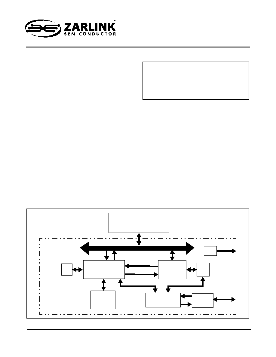
Figure 1 - System Block Diagram
FDB Interface
Frame Data Buffer A
SRAM (1 M / 2 M)
LED
Search
Engine
MCT
Link
Frame Engine
FCB
Management
Module
16 x 10/100M
RMII
Ports 0 - 15
VLAN
1 MCT
16-bit
Parallel /
Serial
ZL50416
Managed 16-Port 10/100M Layer-2
Ethernet Switch
Data Sheet

ZL50416
Data Sheet
2
Zarlink Semiconductor Inc.
� Buffer management: per-class, shared, and per-port buffer reservations
�
Classification based on:
� Port-based priority: priority in a frame can be overwritten by the priority of port
� VLAN Priority field in VLAN tagged frame (IEEE 802.1p)
� DS/TOS field in IP packet
� UDP/TCP logical ports: 8 hard-wired and 8 programmable ports, including one programmable range
�
The drop precedence of the above classifications is programmable
�
Supports IEEE 802.3ad link aggregation
�
2
port trunking groups
� two groups for 10/100 ports, with up to 4 ports per group
� Load sharing among trunked ports can be based on:
- Source and/or destination MAC address
�
Port Mirroring
� supports 2 mirroring ports in managed mode
� supports a dedicated mirroring port in unmanaged mode
�
Built-in MIB statistics counters
�
Full Duplex Ethernet IEEE 802.3x Flow Control
�
Backpressure flow control for Half Duplex ports
�
Full set of LED signals provided by a serial interface
�
Recognizes Simple Bandwidth Management (SBM) and Resource Reservation Protocol (RSVP) packets
and forwards to CPU
�
Built-in reset logic triggered by system malfunction
�
Built-in self test (BIST) for internal and external SRAM

ZL50416
Data Sheet
3
Zarlink Semiconductor Inc.
Description
The ZL50416 is a high density, low cost, high performance, non-blocking Ethernet switch chip. A single chip
provides 16 ports at 10/100 Mbps and a CPU interface for managed and unmanaged switch applications.
The chip supports up to 64K MAC addresses and up to 255 tagged-based Virtual LANs (VLANs). The centralized
shared memory architecture permits a very high performance packet forwarding rate at full wire speed. The chip is
optimized to provide low-cost, high-performance workgroup switching.
A Frame Buffer Memory domain utilizes cost-effective, high-performance synchronous SRAM with aggregate
bandwidth of 6.4 Gbps to support full wire speed on all ports simultaneously.
With delay bounded, strict priority, and/or WFQ transmission scheduling and WRED dropping schemes, the
ZL50416 provides powerful QoS functions for various multimedia and mission-critical applications. The chip
provides 4 transmission priorities and 2 levels of dropping precedence. Each packet is assigned a transmission
priority and dropping precedence based on the VLAN priority field in a VLAN tagged frame, or the DS/TOS field, or
the UDP/TCP logical port fields in IP packets. The ZL50416 recognizes a total of 16 UDP/TCP logical ports, 8 hard-
wired and 8 programmable (including one programmable range).
The ZL50416 supports 2 groups of port trunking/load sharing. Two groups are dedicated to 10/100 ports, where
each 10/100 group can contain up to 4 ports. Port trunking/load sharing can be used to group ports between
interlinked switches to increase the effective network bandwidth.
In half-duplex mode all ports support backpressure flow control to minimize the risk of losing data during long
activity bursts. In full-duplex mode, IEEE 802.3x flow control is provided. The ZL50416 also supports a per-system
option to enable flow control for best effort frames, even on QoS-enabled ports.
Statistical information for SNMP and the Remote Monitoring Management Information Base (RMON MIB) are
collected independently for all ports. Access to these statistical counters/registers is provided via the CPU interface.
SNMP Management frames can be received and transmitted via the CPU interface creating a complete network
management solution.
The ZL50416 is fabricated using 0.25 micron technology. Inputs, however, are 3.3 V tolerant, and the outputs are
capable of directly interfacing to LVTTL levels. The ZL50416 is packaged in a 553-pin Ball Grid Array package.

ZL50416
Data Sheet
4
Zarlink Semiconductor Inc.
Changes Summary
The April 2006 issue is the starting point for the change summary section.
Revision Date
Summary of Changes
April 2006
- Corrected ZL5041x ordering codes (should be /GKC)
- Added Pb-free order code (ZL50416GKG2)
- Corrected TSTOUT6 boostrap description, and clarified only applicable in
"managed" mode
- Corrected ECR1Pn default value (should be 0xC0)
- Corrected PR100 default value (should be 0x35)
- Corrected SFCB default value (should be 0x46)
- Corrected CPU addresses for registers CPUQOSC1,2,3

ZL50416
Data Sheet
Table of Contents
5
Zarlink Semiconductor Inc.
1.0 BGA and Ball Signal Descriptions . . . . . . . . . . . . . . . . . . . . . . . . . . . . . . . . . . . . . . . . . . . . . . . . . . . . . . . . 12
1.1 BGA Views (Top-View) . . . . . . . . . . . . . . . . . . . . . . . . . . . . . . . . . . . . . . . . . . . . . . . . . . . . . . . . . . . . . . . 12
1.1.1 Encapsulated view in managed mode . . . . . . . . . . . . . . . . . . . . . . . . . . . . . . . . . . . . . . . . . . . . . . . 12
1.1.2 Encapsulated view in unmanaged mode . . . . . . . . . . . . . . . . . . . . . . . . . . . . . . . . . . . . . . . . . . . . . 13
1.2 Ball � Signal Descriptions . . . . . . . . . . . . . . . . . . . . . . . . . . . . . . . . . . . . . . . . . . . . . . . . . . . . . . . . . . . . . 14
1.3 Ball � Signal Name . . . . . . . . . . . . . . . . . . . . . . . . . . . . . . . . . . . . . . . . . . . . . . . . . . . . . . . . . . . . . . . . . . 23
1.4 Signal Mapping and Internal Pull Up/Down Configuration. . . . . . . . . . . . . . . . . . . . . . . . . . . . . . . . . . . . . 29
2.0 Block Functionality . . . . . . . . . . . . . . . . . . . . . . . . . . . . . . . . . . . . . . . . . . . . . . . . . . . . . . . . . . . . . . . . . . . . 31
2.1 Frame Data Buffer (FDB) Interfaces . . . . . . . . . . . . . . . . . . . . . . . . . . . . . . . . . . . . . . . . . . . . . . . . . . . . . 31
2.2 MAC Modules . . . . . . . . . . . . . . . . . . . . . . . . . . . . . . . . . . . . . . . . . . . . . . . . . . . . . . . . . . . . . . . . . . . . . . 31
2.2.1 RMII MAC Module (RMAC) . . . . . . . . . . . . . . . . . . . . . . . . . . . . . . . . . . . . . . . . . . . . . . . . . . . . . . . 31
2.2.1.1 GPSI Interface . . . . . . . . . . . . . . . . . . . . . . . . . . . . . . . . . . . . . . . . . . . . . . . . . . . . . . . . . . . . 31
2.2.1.2 SCANLINK and SCANCOL interface . . . . . . . . . . . . . . . . . . . . . . . . . . . . . . . . . . . . . . . . . . . 33
2.2.2 CPU MAC Module (CMAC) . . . . . . . . . . . . . . . . . . . . . . . . . . . . . . . . . . . . . . . . . . . . . . . . . . . . . . . 33
2.2.3 PHY Addresses . . . . . . . . . . . . . . . . . . . . . . . . . . . . . . . . . . . . . . . . . . . . . . . . . . . . . . . . . . . . . . . . 33
2.3 Management Module . . . . . . . . . . . . . . . . . . . . . . . . . . . . . . . . . . . . . . . . . . . . . . . . . . . . . . . . . . . . . . . . 33
2.4 Frame Engine . . . . . . . . . . . . . . . . . . . . . . . . . . . . . . . . . . . . . . . . . . . . . . . . . . . . . . . . . . . . . . . . . . . . . . 34
2.5 Search Engine . . . . . . . . . . . . . . . . . . . . . . . . . . . . . . . . . . . . . . . . . . . . . . . . . . . . . . . . . . . . . . . . . . . . . 34
2.6 LED Interface. . . . . . . . . . . . . . . . . . . . . . . . . . . . . . . . . . . . . . . . . . . . . . . . . . . . . . . . . . . . . . . . . . . . . . . 34
2.6.1 Port Status . . . . . . . . . . . . . . . . . . . . . . . . . . . . . . . . . . . . . . . . . . . . . . . . . . . . . . . . . . . . . . . . . . . . 34
2.6.2 LED Interface Timing Diagram. . . . . . . . . . . . . . . . . . . . . . . . . . . . . . . . . . . . . . . . . . . . . . . . . . . . . 35
2.7 Internal Memory . . . . . . . . . . . . . . . . . . . . . . . . . . . . . . . . . . . . . . . . . . . . . . . . . . . . . . . . . . . . . . . . . . . . 35
2.8 Timeout Reset Monitor . . . . . . . . . . . . . . . . . . . . . . . . . . . . . . . . . . . . . . . . . . . . . . . . . . . . . . . . . . . . . . . 35
3.0 System Configuration (Stand-alone and Stacking) . . . . . . . . . . . . . . . . . . . . . . . . . . . . . . . . . . . . . . . . . . 36
3.1 Management and Configuration . . . . . . . . . . . . . . . . . . . . . . . . . . . . . . . . . . . . . . . . . . . . . . . . . . . . . . . . 36
3.2 Managed Mode . . . . . . . . . . . . . . . . . . . . . . . . . . . . . . . . . . . . . . . . . . . . . . . . . . . . . . . . . . . . . . . . . . . . . 36
3.2.1 Register Configuration, Frame Transmission, and Frame Reception . . . . . . . . . . . . . . . . . . . . . . . 36
3.2.1.1 Register Configuration . . . . . . . . . . . . . . . . . . . . . . . . . . . . . . . . . . . . . . . . . . . . . . . . . . . . . . 36
3.2.1.2 Rx/Tx of Standard Ethernet Frames. . . . . . . . . . . . . . . . . . . . . . . . . . . . . . . . . . . . . . . . . . . . 37
3.2.1.3 Control Frames. . . . . . . . . . . . . . . . . . . . . . . . . . . . . . . . . . . . . . . . . . . . . . . . . . . . . . . . . . . . 37
3.3 Unmanaged Mode . . . . . . . . . . . . . . . . . . . . . . . . . . . . . . . . . . . . . . . . . . . . . . . . . . . . . . . . . . . . . . . . . . . 38
3.3.1 I2C Interface. . . . . . . . . . . . . . . . . . . . . . . . . . . . . . . . . . . . . . . . . . . . . . . . . . . . . . . . . . . . . . . . . . . 38
3.3.1.1 Start Condition . . . . . . . . . . . . . . . . . . . . . . . . . . . . . . . . . . . . . . . . . . . . . . . . . . . . . . . . . . . . 38
3.3.1.2 Address . . . . . . . . . . . . . . . . . . . . . . . . . . . . . . . . . . . . . . . . . . . . . . . . . . . . . . . . . . . . . . . . . 38
3.3.1.3 Data Direction. . . . . . . . . . . . . . . . . . . . . . . . . . . . . . . . . . . . . . . . . . . . . . . . . . . . . . . . . . . . . 38
3.3.1.4 Acknowledgment . . . . . . . . . . . . . . . . . . . . . . . . . . . . . . . . . . . . . . . . . . . . . . . . . . . . . . . . . . 39
3.3.1.5 Data . . . . . . . . . . . . . . . . . . . . . . . . . . . . . . . . . . . . . . . . . . . . . . . . . . . . . . . . . . . . . . . . . . . . 39
3.3.1.6 Stop Condition . . . . . . . . . . . . . . . . . . . . . . . . . . . . . . . . . . . . . . . . . . . . . . . . . . . . . . . . . . . . 39
3.3.2 Synchronous Serial Interface . . . . . . . . . . . . . . . . . . . . . . . . . . . . . . . . . . . . . . . . . . . . . . . . . . . . . . 39
3.3.2.1 Write Command . . . . . . . . . . . . . . . . . . . . . . . . . . . . . . . . . . . . . . . . . . . . . . . . . . . . . . . . . . . 40
3.3.2.2 Read Command . . . . . . . . . . . . . . . . . . . . . . . . . . . . . . . . . . . . . . . . . . . . . . . . . . . . . . . . . . . 40
4.0 Data Forwarding Protocol . . . . . . . . . . . . . . . . . . . . . . . . . . . . . . . . . . . . . . . . . . . . . . . . . . . . . . . . . . . . . . . 40
4.1 Unicast Data Frame Forwarding . . . . . . . . . . . . . . . . . . . . . . . . . . . . . . . . . . . . . . . . . . . . . . . . . . . . . . . . 40
4.2 Multicast Data Frame Forwarding . . . . . . . . . . . . . . . . . . . . . . . . . . . . . . . . . . . . . . . . . . . . . . . . . . . . . . 41
4.3 Frame Forwarding To and From CPU . . . . . . . . . . . . . . . . . . . . . . . . . . . . . . . . . . . . . . . . . . . . . . . . . . . . 41
5.0 Memory Interface . . . . . . . . . . . . . . . . . . . . . . . . . . . . . . . . . . . . . . . . . . . . . . . . . . . . . . . . . . . . . . . . . . . . . . 42
5.1 Overview . . . . . . . . . . . . . . . . . . . . . . . . . . . . . . . . . . . . . . . . . . . . . . . . . . . . . . . . . . . . . . . . . . . . . . . . . . 42
5.2 Memory Requirements . . . . . . . . . . . . . . . . . . . . . . . . . . . . . . . . . . . . . . . . . . . . . . . . . . . . . . . . . . . . . . . 42
5.3 Memory Configurations . . . . . . . . . . . . . . . . . . . . . . . . . . . . . . . . . . . . . . . . . . . . . . . . . . . . . . . . . . . . . . . 43
6.0 Search Engine . . . . . . . . . . . . . . . . . . . . . . . . . . . . . . . . . . . . . . . . . . . . . . . . . . . . . . . . . . . . . . . . . . . . . . . . 45
6.1 Search Engine Overview . . . . . . . . . . . . . . . . . . . . . . . . . . . . . . . . . . . . . . . . . . . . . . . . . . . . . . . . . . . . . 45