 | –≠–ª–µ–∫—Ç—Ä–æ–Ω–Ω—ã–π –∫–æ–º–ø–æ–Ω–µ–Ω—Ç: ZL60105 | –°–∫–∞—á–∞—Ç—å:  PDF PDF  ZIP ZIP |
1
Zarlink Semiconductor Inc.
Zarlink, ZL and the Zarlink Semiconductor logo are trademarks of Zarlink Semiconductor Inc.
Copyright 2003, Zarlink Semiconductor Inc. All Rights Reserved.
Features
∑ 12 parallel channels, total 19.2 Gbps capacity
∑ Data rate up to 1.6 Gbps per channel
∑ 850 nm VCSEL array
∑ Data I/O is CML compatible with DC blocking
capacitors
∑ Link reach up to 1000 m
∑ Channel BER better than 10
-12
∑ Industry standard MPO/MTP
ribbon fiber
connector interface
∑ Pluggable MegArray
Æ
ball grid array connector
∑ Optionally available with EMI shield and external
heat sink
∑ Laser class 1M IEC 60825-1:2001 compliant
∑ Power supply 3.3 V
∑ Compatible with industry MSA
Applications
∑ High-speed interconnects within and between
switches, routers and transport equipment
∑ Proprietary backplanes
∑ Low cost SONET/SDH VSR (Very Short Reach)
OC-192/STM64 connections
∑ InfiniBand
Æ
connections
∑ Interconnects rack-to-rack, shelf-to-shelf, board-
to-board, board-to-optical backplane
Description
The ZL60105 and ZL60106 together make a very high
speed transmitter/receiver pair for parallel fiber
applications.
The transmitter module converts parallel electrical input
signals via a laser driver and a VCSEL array into
parallel optical output signals at a wavelength of
850nm.
The receiver module converts parallel optical input
signals via a PIN photodiode array and a
transimpedance and limiting amplifier into electrical
output signals.
The modules are pluggable each fitted with an industry-
standard MegArray
Æ
BGA connector. This provides
ease of assembly on the host board and enables
provisioning of bandwidth on demand.
October 2003
Ordering Information
ZL60105/MJD Parallel Fiber Transmitter
ZL60106/MJD Parallel Fiber Receiver
Heat sink and EMI shield options
are available upon request
0
∞
C to +80
∞
C
ZL60105/6
12 x 1.6 Gbps Parallel Fiber Optic Link
Transmitter and Receiver
Data Sheet

ZL60105/6
Data Sheet
Table of Contents
2
Zarlink Semiconductor Inc.
Features . . . . . . . . . . . . . . . . . . . . . . . . . . . . . . . . . . . . . . . . . . . . . . . . . . . . . . . . . . . . . . . . . . . . . . . . . . . . . . . . . 1
Applications . . . . . . . . . . . . . . . . . . . . . . . . . . . . . . . . . . . . . . . . . . . . . . . . . . . . . . . . . . . . . . . . . . . . . . . . . . . . . 1
Description . . . . . . . . . . . . . . . . . . . . . . . . . . . . . . . . . . . . . . . . . . . . . . . . . . . . . . . . . . . . . . . . . . . . . . . . . . . . . . 1
Absolute Maximum Ratings . . . . . . . . . . . . . . . . . . . . . . . . . . . . . . . . . . . . . . . . . . . . . . . . . . . . . . . . . . . . . . . . . 3
Recommended Operating Conditions . . . . . . . . . . . . . . . . . . . . . . . . . . . . . . . . . . . . . . . . . . . . . . . . . . . . . . . . . 3
Transmitter Specifications . . . . . . . . . . . . . . . . . . . . . . . . . . . . . . . . . . . . . . . . . . . . . . . . . . . . . . . . . . . . . . . . . . 4
Transmitter Control and Status Signals . . . . . . . . . . . . . . . . . . . . . . . . . . . . . . . . . . . . . . . . . . . . . . . . . . . . . . 6
Transmitter Control and Status Timing Diagrams . . . . . . . . . . . . . . . . . . . . . . . . . . . . . . . . . . . . . . . . . . . . . . 7
Transmitter Pinout Assignments . . . . . . . . . . . . . . . . . . . . . . . . . . . . . . . . . . . . . . . . . . . . . . . . . . . . . . . . . . . . 9
Transmitter Pin Description . . . . . . . . . . . . . . . . . . . . . . . . . . . . . . . . . . . . . . . . . . . . . . . . . . . . . . . . . . . . . . . 9
Receiver Specifications . . . . . . . . . . . . . . . . . . . . . . . . . . . . . . . . . . . . . . . . . . . . . . . . . . . . . . . . . . . . . . . . . . . 10
Receiver Control and Status Signals . . . . . . . . . . . . . . . . . . . . . . . . . . . . . . . . . . . . . . . . . . . . . . . . . . . . . . . 11
Receiver Control and Status Timing Diagrams . . . . . . . . . . . . . . . . . . . . . . . . . . . . . . . . . . . . . . . . . . . . . . . 12
Receiver Pinout Assignments . . . . . . . . . . . . . . . . . . . . . . . . . . . . . . . . . . . . . . . . . . . . . . . . . . . . . . . . . . . . . 13
Receiver Pin Description . . . . . . . . . . . . . . . . . . . . . . . . . . . . . . . . . . . . . . . . . . . . . . . . . . . . . . . . . . . . . . . . 13
Thermal Characteristics . . . . . . . . . . . . . . . . . . . . . . . . . . . . . . . . . . . . . . . . . . . . . . . . . . . . . . . . . . . . . . . . . . . 14
Regulatory Compliance . . . . . . . . . . . . . . . . . . . . . . . . . . . . . . . . . . . . . . . . . . . . . . . . . . . . . . . . . . . . . . . . . . . 15
Eye safety . . . . . . . . . . . . . . . . . . . . . . . . . . . . . . . . . . . . . . . . . . . . . . . . . . . . . . . . . . . . . . . . . . . . . . . . . . . . 15
Electrostatic discharge . . . . . . . . . . . . . . . . . . . . . . . . . . . . . . . . . . . . . . . . . . . . . . . . . . . . . . . . . . . . . . . . . . 15
Electrostatic discharge immunity . . . . . . . . . . . . . . . . . . . . . . . . . . . . . . . . . . . . . . . . . . . . . . . . . . . . . . . . . . 15
Electromagnetic interference . . . . . . . . . . . . . . . . . . . . . . . . . . . . . . . . . . . . . . . . . . . . . . . . . . . . . . . . . . . . . 15
Emission . . . . . . . . . . . . . . . . . . . . . . . . . . . . . . . . . . . . . . . . . . . . . . . . . . . . . . . . . . . . . . . . . . . . . . . . . . 15
Immunity . . . . . . . . . . . . . . . . . . . . . . . . . . . . . . . . . . . . . . . . . . . . . . . . . . . . . . . . . . . . . . . . . . . . . . . . . . 15
Handling instructions . . . . . . . . . . . . . . . . . . . . . . . . . . . . . . . . . . . . . . . . . . . . . . . . . . . . . . . . . . . . . . . . . . . . . 15
Cleaning the optical interface . . . . . . . . . . . . . . . . . . . . . . . . . . . . . . . . . . . . . . . . . . . . . . . . . . . . . . . . . . . . . 15
Connectors . . . . . . . . . . . . . . . . . . . . . . . . . . . . . . . . . . . . . . . . . . . . . . . . . . . . . . . . . . . . . . . . . . . . . . . . . . . 15
ESD handling . . . . . . . . . . . . . . . . . . . . . . . . . . . . . . . . . . . . . . . . . . . . . . . . . . . . . . . . . . . . . . . . . . . . . . . . . 15
Link Reach . . . . . . . . . . . . . . . . . . . . . . . . . . . . . . . . . . . . . . . . . . . . . . . . . . . . . . . . . . . . . . . . . . . . . . . . . . . . . . 16
Link Model Parameters . . . . . . . . . . . . . . . . . . . . . . . . . . . . . . . . . . . . . . . . . . . . . . . . . . . . . . . . . . . . . . . . . . 16
Electrical Interface - Application Examples . . . . . . . . . . . . . . . . . . . . . . . . . . . . . . . . . . . . . . . . . . . . . . . . . . . 17

ZL60105/6
Data Sheet
3
Zarlink Semiconductor Inc.
Absolute Maximum Ratings
Not necessarily applied together. Exceeding these values may cause permanent damage. Functional operation
under these conditions is not implied.
Recommended Operating Conditions
These parameters apply both to the transmitter and the receiver.
Figure 1 - Recommended Power Supply Filter
Parameter
Symbol
Min
Max
Unit
Supply voltage
V
CC
-0.3
4.0
V
Differential input voltage amplitude
1
1. Differential input voltage amplitude is defined as
V =
DIN+
-
DIN-
.
V
1.2
V
Voltage on any pin
V
PIN
-0.3
V
CC
+ 0.3
V
Relative humidity (non-condensing)
M
OS
5
95
%
Storage temperature
T
STG
-40
100
∞
C
ESD resistance
V
ESD
±1
kV
Table 1 - Absolute Maximum Ratings
Parameter
Symbol
Min
Max
Unit
Power supply voltage
V
CC
3.135
3.465
V
Operating case temperature
T
CASE
0
80
∞
C
Signaling rate (per channel)
1
1. Data patterns are to have maximum run lengths and DC balance shifts no worse than that of a Pseudo Random Bit Sequence of
length 2
23
-1 (PRBS-23). Information on lower bit rates is available on request.
f
D
0.5
1.6
Gbps
Link distance
2
2. For maximum distance, see Table 14.
LD
2
m
Data I/O DC blocking capacitors
3
3. For AC-coupling, DC blocking capacitors external to the module with a minimum value of 100 nF is recommended.
C
BLK
100
nF
Power supply noise
4
4. Power supply noise is defined at the supply side of the recommended filter for all V
CC
supplies over the frequency range of 500 Hz
to 1600 MHz with the recommended power supply filter in place.
V
NPS
200
mV
p-p
Table 2 - Recommended Operating Conditions
Host
Vcc
R1 100
C1
10
µ
F
C2
10
µ
F
L1 1
µ
H
R2 1.0 k
C3
0.1
µ
F
C4
0.1
µ
F
L2 6.8 nH
Module
Vcc

ZL60105/6
Data Sheet
4
Zarlink Semiconductor Inc.
Transmitter Specifications
All parameters below require operating conditions according to Table 2 - "Recommended Operating Conditions".
Parameter
Symbol
Min
Max
Unit
Optical Parameters
Launch power (50/125
µ
m MMF)
1
1. The output optical power is compliant with IEC 60825-1 Amendment 2, Class 1M Accessible Emission Limits.
P
OUT
-8
-2
dBm
Extinguished output power
P
OFF
-30
dBm
Extinction ratio
2
2. The extinction ratio is measured at 622 Mbps.
ER
7
dB
Optical modulation amplitude
3
3. Informative. Corresponds to P
OUT
= -8 dBm and ER = 7 dB.
OMA
0.21
mW
Center wavelength
C
830
860
nm
Spectral width
4
4. Spectral width is measured as defined in EIA/TIA-455-127 Spectral Characterization of Multimode Laser Diodes.
0.85
nm
rms
Relative intensity noise OMA
RIN
12
OMA
-116
dB/Hz
Optical output rise time (20 - 80%)
t
RO
255
ps
Optical output fall time (20 - 80%)
t
FO
255
ps
Total jitter contributed (peak to peak)
5
5. Total jitter equals TP1 to TP2 as defined in IEEE 802.3 clauses 38.2 and 38.6 (Gigabit Ethernet).
TJ
200
ps
Deterministic jitter contributed (peak to peak)
DJ
85
ps
Channel to channel skew
6
6. Channel skew is defined for the condition of equal amplitude, zero ps skew signals applied to the transmitter inputs.
t
SK
150
ps
Electrical Parameters
Power dissipation
P
D
1.5
W
Supply current
I
CC
450
mA
Differential input voltage amplitude (peak to peak)
7
7. Differential input voltage is defined as the peak to peak value of the differential voltage between DIN+ and DIN-. Data inputs are
CML compatible.
V
IN
200
1600
mV
p-p
Differential input impedance
8
8. Differential input impedance is measured between DIN+ and DIN-.
Z
IN
80
120
Electrical input rise time (20 - 80%)
t
RE
270
ps
Electrical input fall time (20 - 80%)
t
FE
270
ps
Table 3 - Transmitter Optical and Electrical Specifications
ZL60105/6
Data Sheet
5
Zarlink Semiconductor Inc.
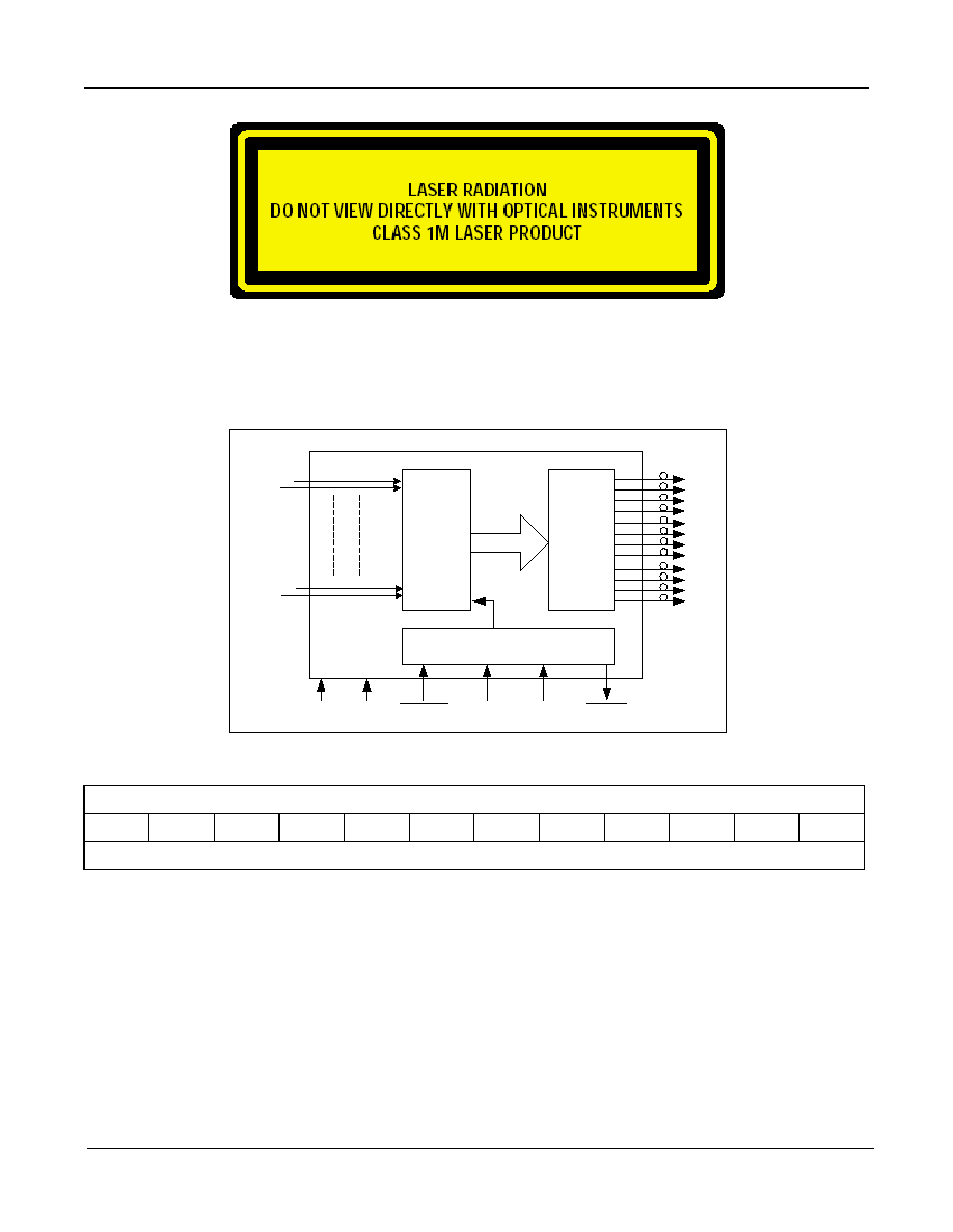
Classified in accordance with IEC 60825-1/A2:2001, IEC 60825-2 : 2000
Class 1M Laser Product
Emited wavelength: 840 nm
Figure 2 - Transmitter Block Diagram
Front view - MTP key up
Ch 11
Ch 10
Ch 9
Ch 8
Ch 7
Ch 6
Ch 5
Ch 4
Ch 3
Ch 2
Ch 1
Ch 0
Host circuit board
Table 4 - Transmitter Optical Channel Assignment
VCSEL Driver Controller
VCSEL
Driver
VCSEL
Array
FAULT
Tx_EN
Tx_DIS
V
CC
V
EE
RESET
DIN0+
DIN0-
DIN11+
DIN11-
0
1
2
3
4
5
6
7
8
9
10
11