 | –≠–ª–µ–∫—Ç—Ä–æ–Ω–Ω—ã–π –∫–æ–º–ø–æ–Ω–µ–Ω—Ç: ZL70010 | –°–∫–∞—á–∞—Ç—å:  PDF PDF  ZIP ZIP |
Document Outline
- Features
- Superior Quality
- Applications
- Description
- Figure 1 - ZL70010 Block Diagram
- Figure 2 - ZL70002 Block Diagram
- Figure 3 - ZL70010 and ZL70002 Bumped Chip Appearance
- Figure 4 - ZL0008/ZL0009 Block Diagram
- Figure 5 - ZL70008 and ZL70009 Bumped Chip Appearance
- 1.0 Functional Description
- 1.1 ZL70010
- 1.2 ZL70002
- 1.3 ZL70008 and ZL70009
- 2.0 Application
- Figure 6 - Pacemaker Application Example
- 2.1 Mechanical Data - ZL70010
- Figure 7 - Size and Bump Placement of ZL70010
- 2.2 Mechanical Data - ZL70002
- Figure 8 - Size and Bump Placement of ZL70002
- 2.3 Mechanical Data - ZL70008 and ZL70009
- Figure 9 - Size and Bump Placement of ZL70008 and ZL70009
- Figure 10 - Bump Appearance of ZL70002/08/09/10
- Figure 11 - 10 ms Surge Current Waveform
- Figure 12 - Terminal to Terminal Characteristic
- Figure 13 - Holding Current Circuit
- Figure 14 - Turn-on Delay Definition
1
Zarlink Semiconductor Inc.
Features
∑
Extremely fast turn-on
∑
Very small size and very low leakage
∑
5, 6 and 7 terminals available
∑
Standard delivery form: solder bumped die
∑
Facilitates compliance with EN-45502 and EN-
50061
Superior Quality
∑
QA procedures based on MIL-PRF-38535
∑
Traceability for every chip to lot and wafer
number
∑
100% burn-in capability
Applications
∑
Pacemakers, Implantable Cardioverter
Defibrillators (ICDs), Neurostimulators, Bladder
Control Devices
∑
Medical devices with electronics requiring
protection against a high voltage surge
Description
The ZL70002/08/09/10 family are high performance
surge protection devices targeted for medical
applications.
July 2003
Ordering Information
ZL70002/UDJ Bumped Die, Waffle Tray
ZL70008/UDJ Bumped Die, Waffle Tray
ZL70009/UDJ Bumped Die, Waffle Tray
ZL70010/UDJ Bumped Die, Waffle Tray
0 to +55
∞
C
ZL70002/08/09/10
Medical Surge Protection Devices
Data Sheet
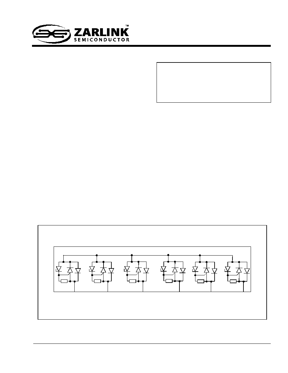
Figure 1 - ZL70010 Block Diagram
Rb
T1
Rb
T2
Rb
T3
Rb
T4
Rb
T5
Rb
T6
ZL70002/08/09/10
Data Sheet
2
Zarlink Semiconductor Inc.
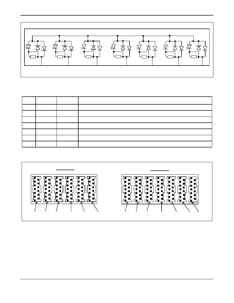
Figure 2 - ZL70002 Block Diagram
Pin Description Table - ZL70010 and ZL70002
Figure 3 - ZL70010 and ZL70002 Bumped Chip Appearance
Pin #
In/Output
Name
Description
1
I
T1
Transient Surge Protection Terminal 1
2
I
T2
Transient Surge Protection Terminal 2
3
I
T3
Transient Surge Protection Terminal 3
4
I
T4
Transient Surge Protection Terminal 4
5
I
T5
Transient Surge Protection Terminal 5
6
I
T6
Transient Surge Protection Terminal 6
7
I
T7
Transient Surge Protection Terminal 7 (ZL70002 only)
Rb
T1
Rb
T2
Rb
T3
Rb
T4
Rb
T5
Rb
T6
Rb
T7
ZL70010
ZL70002
T1
T2
T3
T4
T5
T6
T1
T2
T3
T4
T5
T6
T7
Data Sheet
ZL70002/08/09/10
3
Zarlink Semiconductor Inc.
Figure 4 - ZL0008/ZL0009 Block Diagram
Figure 5 - ZL70008 and ZL70009 Bumped Chip Appearance
Pin Description Table - ZL0008 and ZL0009
Pin #
In/Output
Name
Description
1
I
T1
Transient Surge Protection Terminal 1
2
I
T2
Transient Surge Protection Terminal 2
3
I/O
SUB1
Transient Surge Protection Substrate Connection 1
4
I
T3
Transient Surge Protection Terminal 3 Doubled Area
5
I/O
SUB2
Transient Surge Protection Substrate Connection 2
6
I
T4
Transient Surge Protection Terminal 4
7
I
T5
Transient Surge Protection Terminal 5
Rb
T1
SUB1
SUB2
Rb
T2
Rb
T3
Rb
T4
Rb
T5
ZL70008
ZL70009
T1
T2
T3
T4
T5
SUB1
SUB2
T1
T2
T3
T4
T5
SUB1
SUB2

ZL70002/08/09/10
Data Sheet
4
Zarlink Semiconductor Inc.
1.0
Functional Description
The ZL70002/08/09/10 is a family of transient surge suppressing devices designed specifically for implanted medical
devices. The device terminals have an extremely low leakage during normal voltages and can therefore be
connected in parallel with the pins of the device it protects. When the voltage rises to dangerous level it then rapidly
turns on and limits the voltage by shunting the current through its thyristors. This makes the ZL70002/08/09/10
family an effective means of compliance with international regulations EN-45502, "Active implantable" and the EN-
50061 "Safety of Implantable Cardiac Pacemakers".
1.1
ZL70010
ZL70010 is a six-branch device.The suppression is achieved by a self-triggering thyristor-diode device in parallel
with a diode between each branch-input and a common node which also is the substrate of the device. The six
branches of the device are reached through terminals T1, T2, T3, T4, T5 and T6. The electrical characteristic
observed between any two of the terminals (T1, T2, T3, T4, T5 and T6) very much resembles that of a DIAC, see
Figure 12.
When a transient current is forced between two branch-input terminals, the positive terminal will be clamped to the
common node by the diode of one branch and the negative terminal to the forward voltage of the thyristor-diode of
the other branch. Due to the low on-state voltage of the thyristor that voltage will stay at a safe value during the
transient.
1.2
ZL70002
ZL70002 is a seven-branch device with exactly the same electrical characteristics as ZL70010.
1.3
ZL70008 and ZL70009
ZL70008 and ZL70009 are five-branch transient surge suppressing with the same functionality as ZL70010. The
only functional difference is that the substrate of the device is accessible through the two terminals SUB1 and SUB2.
Data Sheet
ZL70002/08/09/10
5
Zarlink Semiconductor Inc.
2.0
Application
According to the EN-45502 standard, all active medical devices intended for implantation in a human torso should
not be permanently affected by an external defibrillation of the patient. Compliance is confirmed if the implanted
device continues to meet device specification after being subjected to a sequence of 140 Volt pulses in series with
a 300 Ohm resistor between each conductive part of the device including the device case (see EN-45502 for
details). Using the ZL70002/08/09/10 protects the implantable device and is an effective means of compliance with
the EN-45502 standard where the electronics, in almost all cases, would be destroyed if not protected. The same
compliance tests are also described in EN-50061.
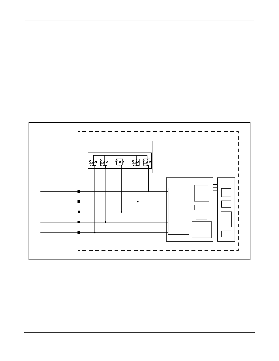
In the application example shown in Figure 6, each of the dual chamber pacemaker's terminals and case are
connected to a terminal on the protection device. If a defibrillation pulse causes the ventricular tip to begin to go
positive, relative to the case, the ZL70008/9 thyristor structure rapidly becomes active and forms a low impedance
path between T2 and T3 to absorb the current and limit the voltage. This provides an effective means of protection
to the pacemaker chip. In actuality, the voltages and currents the implanted device is subjected to in an actual
defibrillation can be higher than described in EN-45502/EN-50061 and has been taken into account when designing
the ZL70002/08/09/10 family.
Figure 6 - Pacemaker Application Example
Terminals placed most remotely to others should get special attention since they effectively form a large pick-up
coil and could therefore be exposed to a large amount of current. When implanted, the pacemaker case is placed
beneath the collarbone and all other terminals are placed together inside the heart. For this reason, the largest
current will pass through the surge protection terminal connected to the case of the pacemaker. For ZL70008/9, we
recommend that the case be connected to T3 of the protection device which is designed to be able to withstand the
largest amount of current. If device ZL700010 is used in a 5 terminal application, we recommend that 2 pins of the
protection device be connected to the implantable device terminal with the largest current flow (typically the terminal
for the device case).
Analog chip
T1
T2
T3
T4
T5
Atrial tip lead
Atrial ring lead
Case
Ventricular tip lead
Ventricular ring lead
Typical Dual Chamber Pacemaker
Surge Protection Device
ZL70008/09
Stimulation
and
block
Charge
Pump
Voltage
and
Current
Reference
Digital
chip
Sensing