 | –≠–ª–µ–∫—Ç—Ä–æ–Ω–Ω—ã–π –∫–æ–º–ø–æ–Ω–µ–Ω—Ç: ZN427J8 | –°–∫–∞—á–∞—Ç—å:  PDF PDF  ZIP ZIP |

THIS DOCUMENT IS FOR MAINTENANCE
PURPOSES ONLY AND IS NOT
RECOMMENDED FOR NEW DESIGNS
ZN427E8 / ZN427J8
MICROPROCESSOR COMPATIBLE
8-BIT SUCCESSIVE APPROXIMATION A-D CONVERTER
DS3006 - 2.1
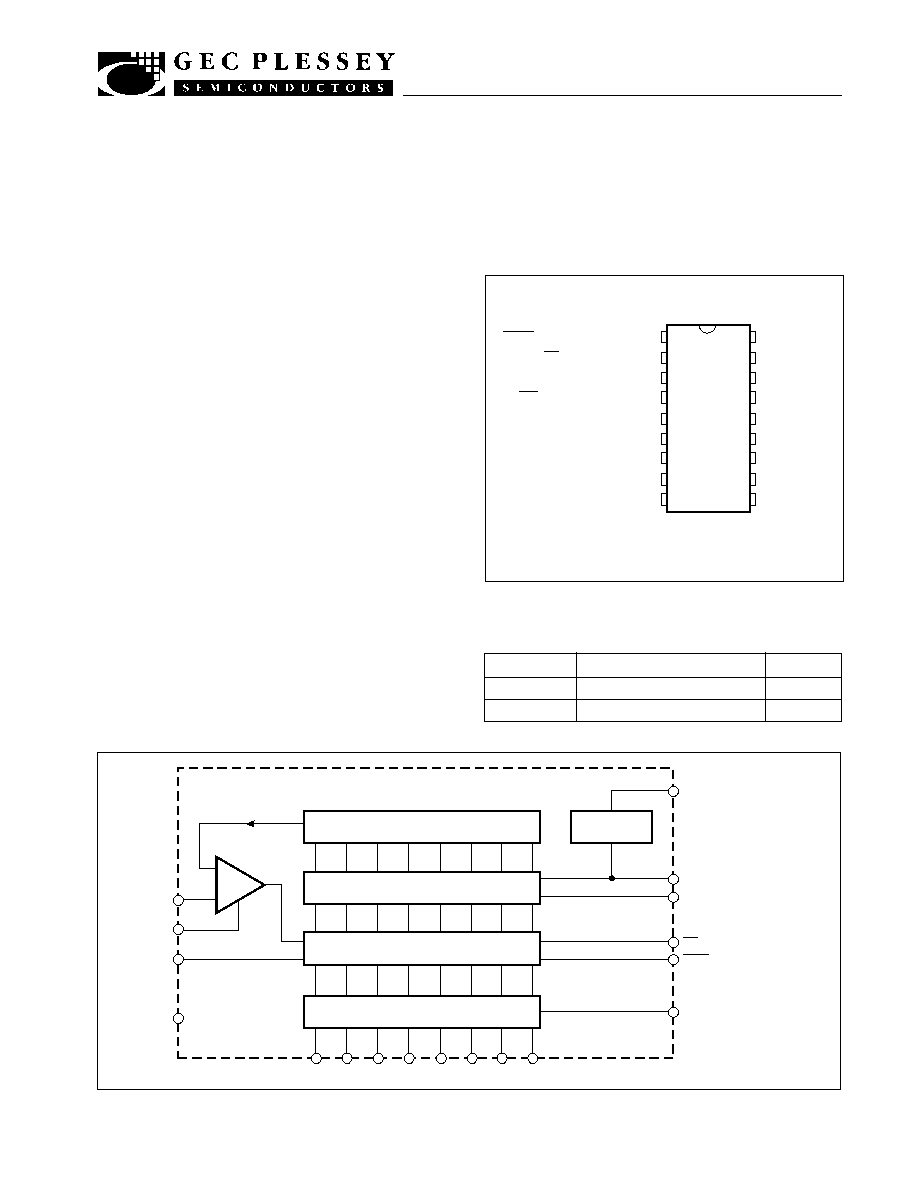
Fig.2 System diagram
The ZN427 is an 8-bit successive approximation converter
with three-state outputs to permit easy interfacing to a
common data bus. The IC contains a voltage switching DAC,
a fast comparator, successive approximation logic and a
2.56V precision bandgap reference, the use of which is pin
optional to retain flexibility. An external fixed or varying
reference may therefore be substituted, thus allowing
ratiometic operation
Only passive external components are required for
operation of the converter.
FEATURES
s
Easy Interfacing to Microprocessor, or Operates as a
'Stand-Alone' Converter
s
Fast: 10 microseconds Conversion time Guaranteed
s
No Missing Codes over Operating Temperature Range
s
Data Outputs Three-State TTL Compatible, other
Logic Inputs and Output TTL and CMOS Compatible
s
Choice of On-Chip or External Reference Voltage
s
Ratiometric Operation
s
Unipolar or Bipolar Input Ranges
s
Complementary to ZN428 DAC
s
Commercial or Military Temperature Range
Fig.1 Pin connection - top view
ORDERING INFORMATION
ZN427J8 (DC18)
ZN427E8 (DP18)
ZN427E8
ZN427J8
DP18
DC18
0
∞
C to +70
∞
C
-55
∞
C to +125
∞
C
Device type
Package
Operating temperature
WR (START CONVERSION)
BUSY (END OF CONVERSION)
BIT 8
(LSB)
RD (OUTPUT ENABLE)
BIT 7
CLOCK
BIT 6
BIT 5
R
EXT
BIT 4
V
IN
BIT 3
V
REF
IN
BIT 2
V
REF
OUT
BIT 1
(MSB)
GROUND
+V
CC
(+5V)
18
1
17
2
16
3
15
4
14
5
13
6
12
7
11
8
10
9
3-STATE BUFFERS
ANALOGUE VOLTAGE SWITCHES
R-2R LADDER
18
17
16
15
14
13
12
LSB
11
MSB
SUCCESSIVE
APPROXIMATION REGISTER
-
+
COMPARATOR
D TO A OUTPUT
VCC
(+5V)
10
CLOCK
INPUT
3
REXT
5
VIN
6
WR (START CONVERSION)
4
VREF IN
7
GROUND
9
VREF OUT
8
RD (OUTPUT ENABLE)
2
BUSY (END CONVERSION)
1
+2.5V
REFERENCE

ZN427
2
ABSOLUTE MAXIMUM RATINGS
Supply voltage V
CC
+7.0V
Max. voltage, logic and V
REF
input
+V
CC
Operating temperature range
0
∞
C to +70
∞
C (ZN427E8)
-55
∞
C to +125
∞
C (ZN427J8)
Storage temperature range
-55
∞
C to +125
∞
C
External Ref. 2.5V
DC Package
DP Package
V
REF IN
= 2.560V
See note 1
V
IN
= +3V, R
EXT
= 82k
V - = -5V
See comparator (page x-xx)
R
REF
= 390
, C
REF
= 4
µ
7
See reference (page x-xx)
V
IN
= 5.5V, V
CC
= max.
V
IN
= 2.4V, V
CC
= max.
V
IN
= 5.5V, V
CC
= max.
V
IN
= 2.4V, V
CC
= max.
V
IN
= 0.4V, V
CC
= max.
I
OH
= max., V
CC
= min.
I
OL
= max., V
CC
= min.
V
O
= 2.4V
See Fig.9
See Fig.9
See note 1
8
-
-
-
-
-
-
12
10
2.545
-
1.5
4.5
-
-
-
-
25
-3.0
-0.5
2.475
-
-
4
2.0
-
-
-
-
-
-
-
-
2.4
-
-
-
-
-
250
-
500
900
-
-
±
0.5
±
3
±
6
±
2.5
±
8
15
13
2.550
-
-
-
25
125
1
100
-
-
-
2.560
0.5
50
-
-
-
-
-
-
-
-
-
-
-
-
-
-
-
180
160
-
-
1000
-
±
0.5
-
-
-
-
-
18
16
2.555
10
3.0
5.5
40
-
-
-
15
-30.0
3.5
2.625
2
-
15
-
0.8
50
15
100
30
-5
-100
1.6
-
0.4
2
-1.5
250
250
-
250
-
-
Min.
Typ.
Max.
Bits
LSB
LSB
ppm/
∞
C
ppm/
∞
C
ppm/
∞
C
µ
V/
∞
C
mV
mV
V
µ
s
V
V
mA
mW
µ
A
k
µ
A
V
V
V
ppm/
∞
C
mA
V
V
µ
A
µ
A
µ
A
µ
A
µ
A
µ
A
mA
V
V
µ
A
V
ns
ns
ns
ns
ns
kHz
Parameter
Units
Conditions
Converter
Resolution
Linearity error
Differential non-linearity
Linearity error T.C.
Differential non-linearity T.C.
Full-scale (gain) T.C.
Zero T.C.
Zero transition
00000000
to 00000001
F.S. transition
11111110
to 11111111
Conversion time
External reference voltage
Supply voltage (V
CC
)
Supply current
Power consumption
Comparator
Input current
Input resistance
Tail current, I
EXT
Negative supply, V≠
Input voltage
Internal voltagee reference
Output voltage
Slope resistance
V
REF
temperature coefficient
Reference current
Logic (over operating temperature range)
High level input voltage V
IH
Low level input voltage V
IL
High level input current,
WR
and RD inputs I
IH
High level input current,
Clock input I
IH
Low level input current I
IL
High level output current I
OH
Low level output current I
OL
High level output voltage V
OH
Low level output voltage V
OL
Disable output leakage
Input clamp diode voltage
Read input to data output
Enable/disable delay time t
RD
Start pulse width tWR
WR
to
BUSY
propagation delay t
BD
Clock pulse width
Maximum clock frequency
ELECTRICAL CHARACTERISTICS
(at V
CC
= 5V, T
amb
= 25
∞
C unless otherwise specified).
Note 1: A 900kHz clock gives a conversion time of 10
µ
s (9 clock periods).
ZN427
3
GENERAL CIRCUIT OPERATION
The ZN427 utilises the successive approximation technique.
Upon receipt of a negative-going pulse at the
WR
input the
BUSY
output goes low, the MSB is set to 1 and all other bits
are set to 0, which produces an output voltage of V
REF/2
from the
DAC. This is compared to the input voltage V
IN
; a decision is
made on the next negative clock edge to reset the
MSB to 0 if > V
IN
or leave it set to 1 if < V
IN
.
Bit 2 is set to 1 on the same clock edge, producing an output
from the DAC of or + depending on the state
of the MSB. This voltage is compared to V
IN
and on the next
clock edge a decision is made regarding bit 2, whilst bit 3 is set
V
REF
2
V
REF
2
V
REF
4
V
REF
2
V
REF
4
to 1. This procedure is repeated for all eight bits. On the ninth
negative clock edge
BUSY
goes high indicating that the
conversion is complete.
During a conversion the RD input will normally be held high to
keep the three-state buffers in their high impedance state.
Data can be read out by taking
RD
high, thus enabling the
three-state output. Readout is non-destructive. The
BUSY
output may be tied to the RD input to automatically enable the
outputs when the data is valid.
For reliable operation of the converter the start pulse applied
to the
WR
input must meet certain timing criteria with respect
to the converter clock. These are detailed in the timing
diagram of Fig.3.
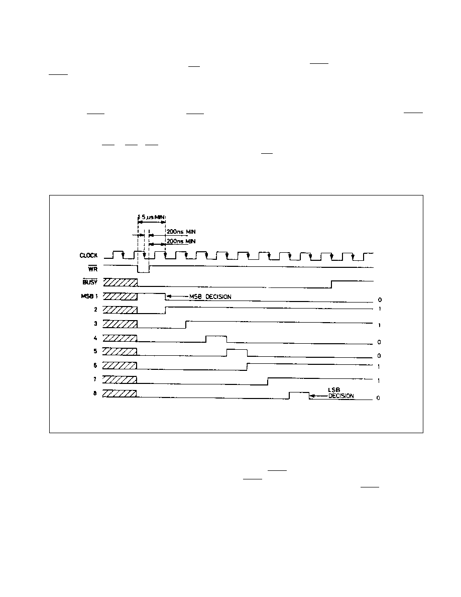
Fig.3 Timing diagram
NOTES ON TIMING DIAGRAM
1. A conversion sequence is shown for the digital word
01100110. For clarity the three-state outputs are shown as
being enabled during the conversion, but normal practice
would be to disable them until the conversion was complete.
2. The
BUSY
output goes low during a conversion. When
BUSY
goes high at the end of a conversion the output data is
valid. In a microprocessor system the
BUSY
output can be
used to generate an interrupt request when the conversion is
complete.
ZN427
4
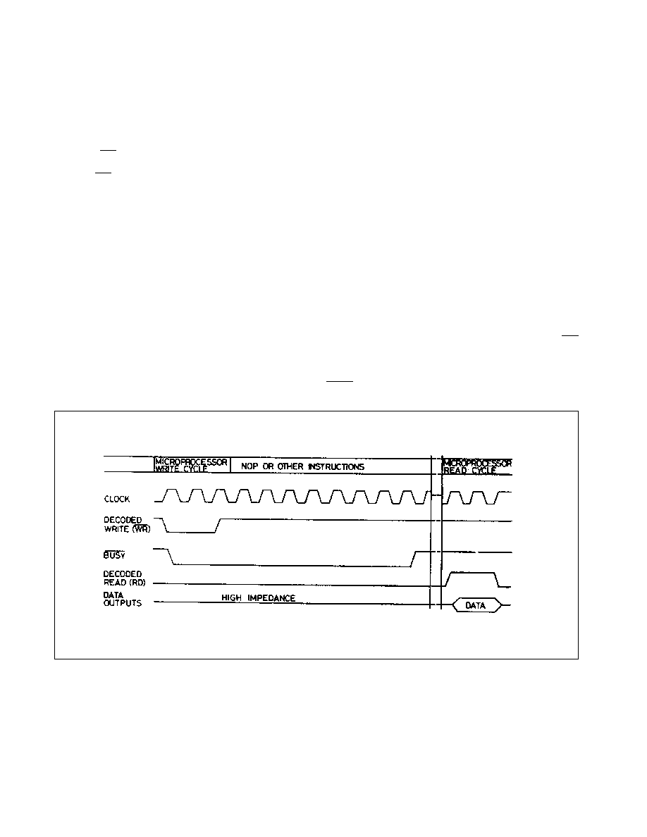
PRACTICAL CLOCK AND SYNCHRONISING
CIRCUITS
The actual method of generating the clock signal and
synchronising it to the start conversion system in which the
ZN427 is incorporated.
When used with a microprocessor the ZN427 can be treated
as RAM and can be assigned a memory address using an
address decoder. If the
µ
P clock is used to drive the ZN427
and the
µ
P write pulse meets the ZN427 timing criteria with
respect to the
µ
P clock then generating the start pulse is
simply a matter of gating the decoded address with the
microprocessor write pulse. Whilst the conversion is being
performed the microprocesor can perform other instructions
or No operation (NOP). when the conversion is complete the
outputs can be enabled onto the bus by gating the decoded
address with the read pulse. A timing diagram for this
sequence of operation is given in Fig.4.
An advantage of using the microprocessor clock is that the
conversion time is known precisely in terms of machine
cycles. the data outputs may therefore be read after a fixed
delay of at least nine clock cycles after the end of the
WR
pulse, when the conversion will be complete.
Alternatively the read operation may be initiated by using the
BUSY
output to generate interrupt request.
3. In the timing diagram cross hatching indicates a 'don't
care' condition.
4. The start pulse operates as an asynchronous
(independent of clock) reset that sets the MSB output to 1 and
sets all other outputs and the end of conversion flag to 0. This
resetting occurs on the low-going edge of the start pulse and
as long as
WR
is low the converter is inhibited. Conversion
commences on the first active (negative going) clock edge
after the
WR
input has gone high again, when the MSB
decision is made. A number of timing constraints thus supply
to the start pulse.
(a) The minimum duration of the start pulse is 250ns, to allow
reliable resetting of the converter logic circuits.
(b) There is no limit to the maximum duration of the start pulse.
(c) To allow the MSB to settle at least 1.5
µ
s must elapse
between the negative going edge of the start pulse and the first
active clock edge that indicates the MSB desicion.
(d) To ensure relaible clocking the positive-going edge of the
start pulse should not occur within 200ns of an active
(negative-going) clock edge. The ideal place for the positive-
going edge of the start pulse is coincident with a positive-going
clock edge. As a special case of the above conditions that
start pulse may be synchronous with a negative-going clock
pulse.
Fig.4 Typical timing diagram using
µ
P clock and write pulse
In some systems, for example single-chip microcomputers
such as the 8048, this simple method may not be feasible for
one or more of the following reasons:
(a) The MPU clock is not available externally.
(b) The clock frequency is too high.

ZN427
5
(c) The write pulse timing criteria make it unsuitable for direct
use as a start conversion pulse.
If any of these conditions apply then the self-synchronising
clock circuit of Fig.5a is recommended.
Fig.5a Self-synchronising clock circuit
Fig.5b Timing diagram for circuit of Fig.5a
ZN427
6
N1 is connected as an astable multivibrator which, when the
BUSY
output is high, is inhibited by the output of N2 holding
one of its inputs low. The start conversion pulse resets the
BUSY
flag and N1 begins to oscillate. When the conversion
is complete
BUSY
goes high and the clock is inhibited.
Since the start pulse starts the clock it may occur at any time.
The only constraints on the start pulse are that it must be
longer than 250ns but at least 200ns shorter than the first clock
pulse. The first clock pulse is in fact longer than the rest since
C1 starts from a fully charged condition whereas on
subsequent cycles it changes between the upper and lower
threshold (V
T+
and V
T
) of the Schmitt trigger.
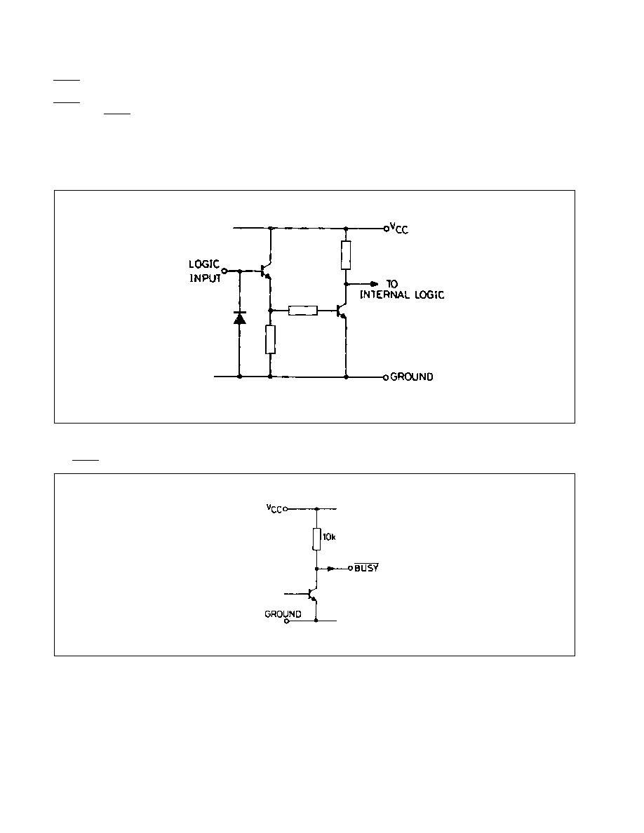
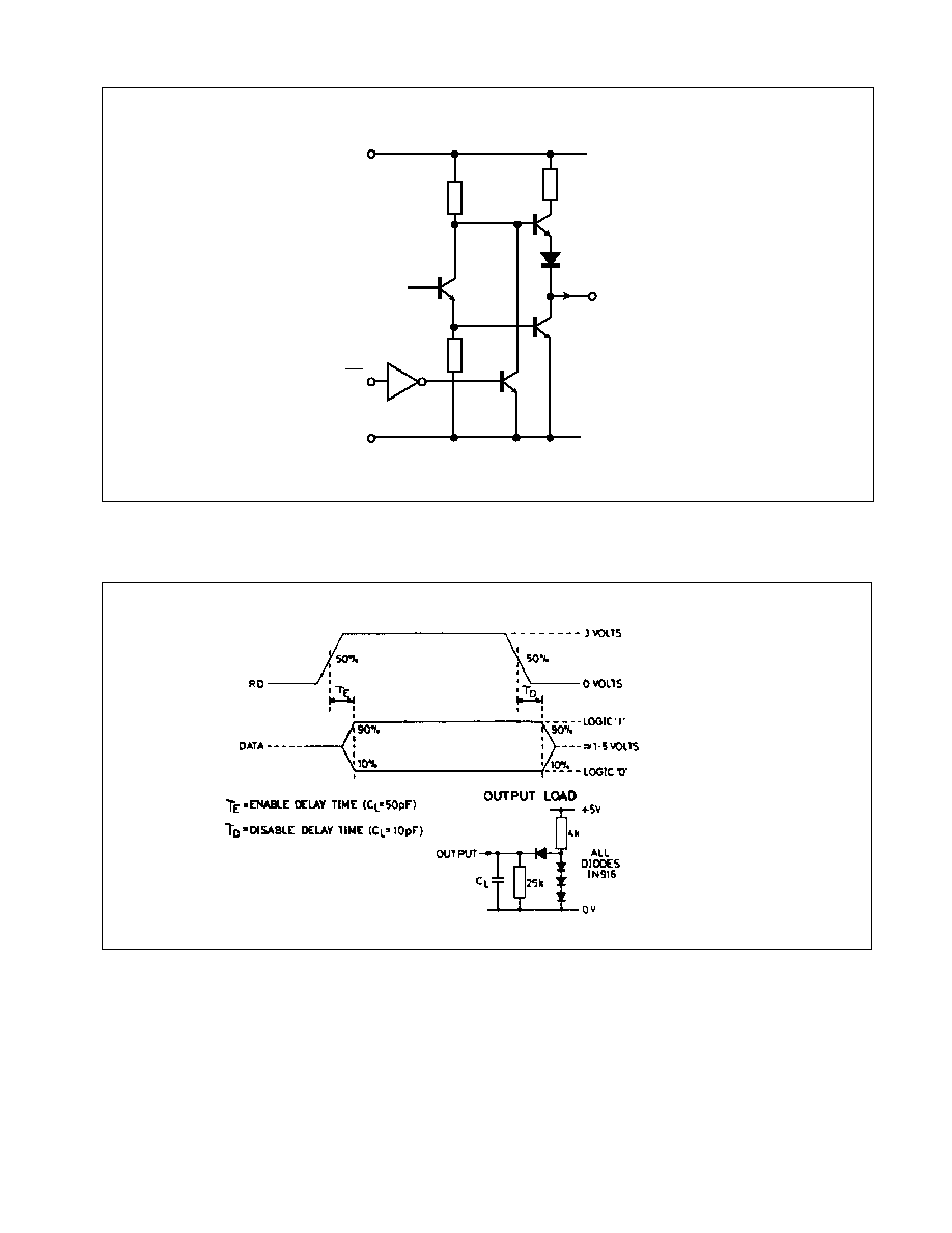
LOGIC INPUTS AND OUTPUTS
The logic inputs of the ZN427 utilise the emitter-follower
configuration shown in Fig.6. This gives extremely low input
currents for CMOS as well as TTL compatibility.
Fig.6 Equivalent circuit of all inputs
Fig.7
The data outputs have three-state buffers, an equivalent
circuit of which is shown in Fig.8. Whilst the RD input is low
both output transistors are turned off and the output is in a high
The
BUSY
output, shown in Fig.7, utilises a passive pullup for CMOS/TTL compatibility.
impedance state. When RD is high the data output will
assume the appropriate logic state (0 or 1).
ZN427
7
Fig.8 Equivalent circuit of data outputs
20k
10k
GROUND
BITS 1-8
(PINS 11-18)
RD
(PIN 2)
VCC
500
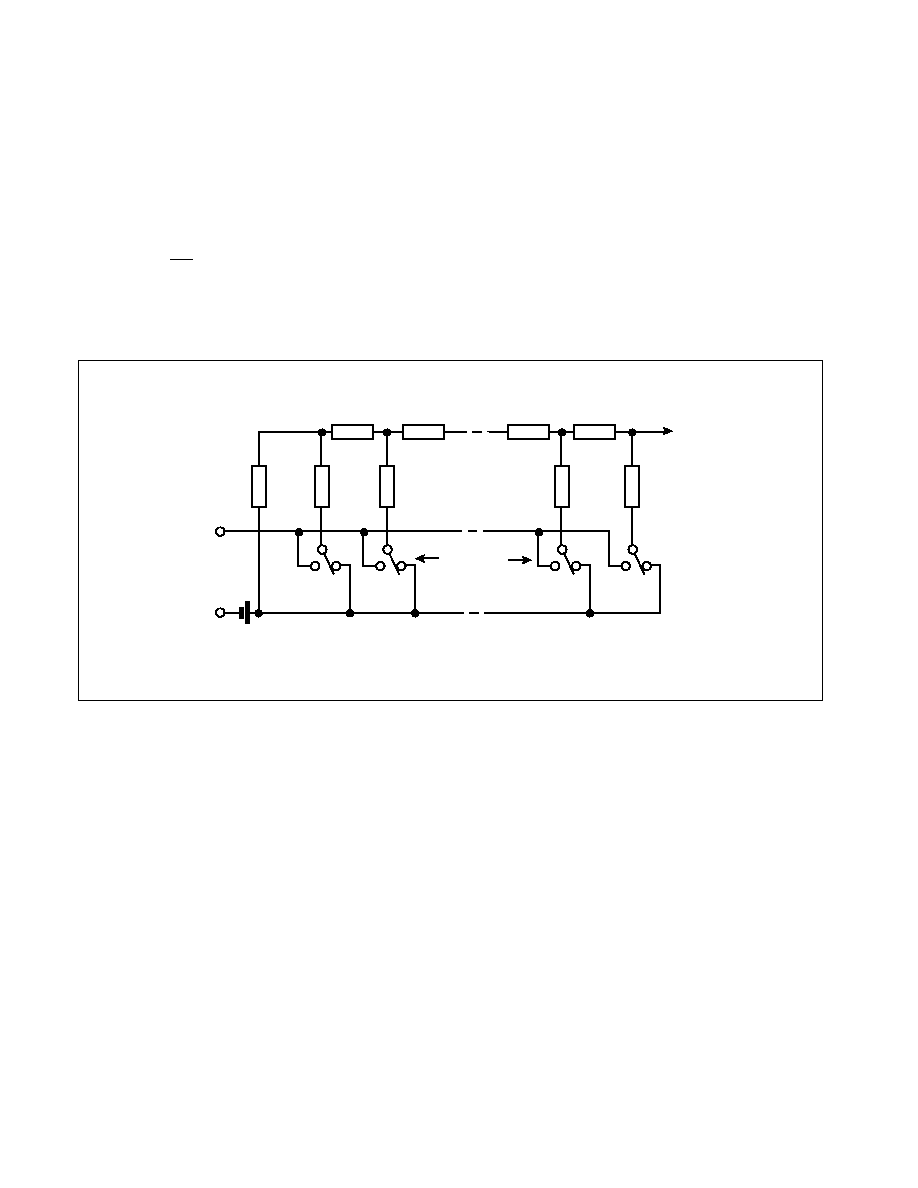
A test circuit and timing diagram for the output enable/disable delays are given in Fig.9.
Fig.9 Output enable/disable waveforms
ZN427
8
ANALOG CIRCUITS
D-A converter
IThe converter is of the voltage switching type and uses an R-
2R ladder network as shown in Fig.10. Each element is
connected to either 0V or V
REF
IN by transistor voltage switches
specially designed for low offset voltage (<1mV).
A binary weighted voltage is produced at the output of the R-
2R ladder.
D to A output = n (V
REF
IN -V
OS
) + V
OS
256
where n is the digital input to the D-A from successive
approximation register.
V
OS
is a small offset voltage that is produced by the device
supply current flowing in the package lead resistance. The
value of V
OS
is typically 2mV for the ZN427E8 and 4mV for the
ZN427J8.
This offset will normally be removed by the setting up
procedure and since the offset temperature coefficient is low
(8
µ
V/
∞
C), the effect on accuaracy will be negligible.
The D-A output range can be considered to be 0 - V
REF IN
through an output resistance R (4k).
REFERENCE
(a) Internal reference
The internal reference is an active bandgap circuit which is
equivalent to a 2.5V Zener diode with a very low slope
impedance (Fig.11). A Resistor (R
REF
) should be connected
between pins 8 and 10. The recommended value of 390
will
supply a nominal reference current of (5.0 - 2.5)/0.39=6.4mA.
A stabilising/decoupling capacitor, C
REF
(4
µ
7), is required
between pins 8 and 9. For internal reference operation V
REF
OUT (pin 8) is connected to V
REF
IN (pin 7).
UP to five ZN427's may be driven from one internal reference,
there being no need to reduce R
REF
. This useful feature saves
power and gives excellent gain tracking between the
converters.
Alternatively the internal reference can be used as the
reference voltage for other external circuits and can source or
sink up to 3mA.
Fig.10 R-2R ladder network
2R
2R
2R
2R
2R
R(4k)
R
R
R
D TO A OUTPUT
BIT 2
BIT 8
VOS
BIT 7
BIT 1
MSB
0 VOLTS
(PIN 9)
VREF IN
(PIN 7)
VOLTAGE
SWITCHES

ZN427
9
GROUND
(PIN 9)
CREF
(4.7µ)
RREF
(390)
VREF OUT
(PIN 8)
VCC +5V
(PIN 10)
Fig.11 Internal voltage reference
(b) External reference
If required an external reference in the range +1.5 to +3.0V
may be connected to V
REF
IN. The slope resistance of such a
reference source should be less than 2.5
, where n is the
n
number of converters supplied.
RATIOMETRIC OPERATION
If the output from a transducer varies with its supply then an
external reference for the ZN427 should be derived from the
same supply. The external reference can vary from +1.5 to
+3.0V. The ZN448/9 will operate if V
REF
IN is less than +1.5V
but reduced overdrive to the comparator will increase its delay
and so the conversion time will need to be increased.
COMPARATOR
The ZN427 contains a fast comparator, the equivalent input
circuit of which is shown in Fig.12.
Fig.12 Comparator equivalent circuit
4k
4k
PIN 5
V -
6k
6k
TO LOGIC
HIGH = 'RETAIN BIT'
D TO A OUTPUT
(O - VREF IN)
AIN
RIN
VIN
PIN 6
+5V PIN 10
REXT
IEXT
+
-
ZN427
10
The comparator derives the tail current, I
EXT
, for its first stage
from an external resistor, R
EXT
, which is taken to a negative
supply V≠.
This arrangement allows the ZN427 to work with any negative
supply in the range -3 to -30 volts. the ZN427 is designed to
be insensitive to changes in I
EXT
from 25
µ
A to 150
µ
A. The
suggested nominal value of I
EXT
is 65
µ
A and a suitable value
for R
EXT
is given by R
EXT
= |V_|15k
.
V
≠
(volts)
-3
-5
-10
-12
-15
-20
-25
-30
R
EXT
(
±
10%)
47k
82k
150k
180k
220k
330k
390k
470k
The output from the D-A converter is connected through the
4k
ladder resistance to one side of the comparator. The
analog input to be converted could be connected directly to the
other comparator input (V
IN
, pin 6) but for optimum stability
with temperature the analog input should be applied through
a source resistance (R
IN
= 4k
) to match the ladder
resistance).
ANALOG INPUT RANGES
The basic connection of the ZN427 shown in Fig.13 has an
analog input range 0 to V
REF
IN which, in some applications,
may be made available from previous signal conditioning/
scaling circuits. Input voltage ranges greater than this are
accommodated by providing an attenuator on the comparator
input, whilst for smaller input ranges the signal must be
amplified to a suitable level.
Bipolar input ranges are accommodated by off-setting the
analog input input range so that the comparator always sees
a positive input voltage.
Fig.13 External components for basic operation
LSB
BIT 8
MSB
BIT 1
VCC
(+5V)
BUSY
1
18
7
RD
2
17
6
CK
3
16
5
WR
4
15
4
V-
(-5V)
5
14
3
AIN
6
13
2
VREFIN
7
12
VREFOUT
8
11
GND
(0V)
9
10
RREF
(390
)
REXT
(82k)
RIN
(4k)
VIN
CREF
(4µ7)
DIGITAL OUTPUTS
NOMINAL AIN RANGE = 0 TO VREFIN

ZN427
11
R
1
R
2
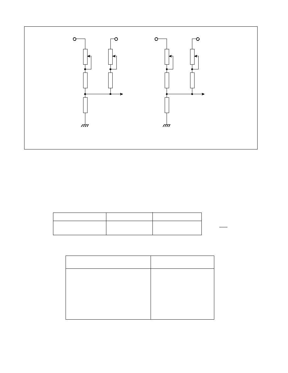
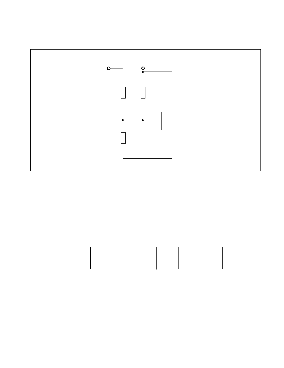
UNIPOLAR OPERATION
The general connection for unipolar operation is shown in
Fig.14.
The values of R
1
and R
2
are chosen so that V
IN
= V
REF
IN when
the analogue input (A
IN
) is at full-scale.
The resulting full-scale range is given by:
A
IN
FS = 1 + , V
REF
IN = G.V
REF
IN.
To match the ladder resistance R
1
/R
2
(R
IN
) = 4k
.
The required nominal values of R
1
and R
2
are given by
R
1
= 4Gk, R
2
= 4G k
G-1
Fig.14 Unipolar operation - general connection
R1
R2
680k
1M
ZERO
ADJUST
GROUND
7
9
6
ZN427
VIN
AIN
VREF IN
Using these relationships a table of nominal values of R
1
and
R
2
can be constructed for V
REF
IN = 2.5V.
Gain adjustment
Due to tolerance in R
1
and R
2
, tolerance in V
REF
and the gain
(full-scale) error of the DAC, some adjustment should be
incorporated into R
1
to calibrate the full-scale of the converter.
When used with the internal reference and 2% resistors a
preset capable of adjusting R
1
by at least
±
5% of its nominal
value is suggested.
R
2
8k
5.33k
R
1
8k
16k
G
2
4
Input range
+5V
+10V
Zero adjustment
Due to offsets in the DAC and comparator the zero (0 to 1)
code transition would occur with typically 15mV applied to the
comparator input, which correpsonds to 1.5LSB with a 2.56V
reference.
Zero adjustment must therefore be provided to set the zero
transition to its correct value of +0.5LSB or 5mV with a 2.56V
reference. This is achieved by applying an adjustable positive
offset to the comparator input via P2 and R3. The values
shown are suitable for all input ranges greater than 1.5 times
V
REF
IN.
Practical circuit values for +5 and +10V input ranges are given
in Fig.15, which incorporates both zero and gain adjustments.
ZN427
12
Fig.15 Unipolar operation - component values
AIN
VREF IN
TO PIN 6
R1 11k
R2 5k6
680k
R3
P2
P1 10k
GAIN
ADJUST
1M
ZERO
ADJUST
± 2% RESISTORS
±20% POTENTIOMETERS
AIN
VREF IN
TO PIN 6
R1 5k6
R2 8k2
680k
R3
P2
P1 5k
GAIN
ADJUST
1M
ZERO
ADJUST
+5V FULL-SCALE
+10V FULL-SCALE
Unipolar adjustment prodedure
(i) Apply continuous convert pulses at intervals long enough
to allow a complete conversion and monitor the digital
outputs.
(ii) Apply full-scale minus 1.5LSB to A
IN
and adjust off-set until
the 8 bit (LSB) output just flickers between 0 and 1 with all
other bits at 0.
(iii) Apply 0.5LSB) to A
IN
and adjust zero until 8 bit just flickers
between 0 and 1 with all other bits at 1.
Unipolar logic coding
Analogue input (A
IN
)
(Nominal code centre value)
FS - 1LSB
FS - 2LSB
0.75FS
0.5FS + 1LSB
0.5FS
0.5FS - 1LSB
0.25FS
1LSB
0
Output code
(offset binary)
11111111
11111110
11000000
10000001
10000000
01111111
01000000
00000001
00000000
1LSB = FS
256
Unipolar setting up points
FS - 1.5LSB
4.9707V
9.9414V
Input range, +FS
+5V
+10V
0.5LSB
9.8mV
19.5mV
ZN427
13
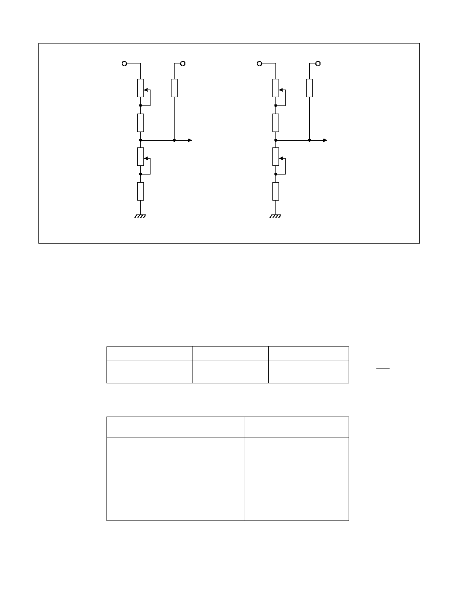
BIPOLAR OPERATION
For bipolar operation the input to the ZN427 is offset by half
full-scale by connecting a resistor R
3
between V
REF
IN and V
IN
(Fig.16).
Fig.16 Bipolar operation - general connection
R1
R3
R2
GROUND
7
9
6
ZN427
VIN
AIN
VREF IN
When A
IN
= -FS, V
IN
needs to be equal to zero.
When A
IN
= +FS, V
IN
needs to be equal to V
REF
IN.
If the full-scale range is
±
G. V
REF
IN then R
1
= (G - 1). R
2
and
R
1
= G. R
3
fulfil the required conditions.
To match the ladder resistance, R
1
/R
2
/R
3
(=R
IN
) = 4k.
Thus the nominal values of R
1
, R
2
, R
3
are given by R
1
= 8 Gk
,
R
2
= 8G/(G - 1)k, R
3
= 8k
.
A bipolar range of
±
V
REF
IN (which corresponds to the basic
unipolar range 0 to +V
REF
IN) results if R
1
= R
3
= 8k
and R
2
=
.
Assuming the V
REF IN
= 2.5V the nominal values of resistors for
±
5 and
±
10V input ranges are given in the following table.
R
2
16k
10.66k
R
1
16k
32k
G
2
4
Input range
+5V
+10V
Minus full-scale (offset) is set by adjusting R
1
about its nominal
value relative to R
3
. Plus full-scale (gain) is set by adjusting R
2
relative to R
1
.
Practical circuit realisations are given in Fig.17.
R
3
8k
8k
Note that in the
±
5V case R
3
has been chosen as 7.5k (instead
of 8.2k) to obtain a more symmetrical range of adjustment
using standard potentiometers.
ZN427
14
Fig.17 Bipolar operation - component values
AIN
VREF
TO PIN 6
13k
7k5
5k
OFFSET
ADJUST
13
5k
GAIN
ADJUST
± 2% RESISTORS
±20% POTENTIOMETERS
±5VOLTS FULL SCALE
AIN
VREF
TO PIN 6
27k
8k2
10k
OFFSET
ADJUST
8k2
5k
GAIN
ADJUST
±10VOLTS FULL SCALE
Bipolar adjustment prodedure
(i) Apply continuous SC pulses at intervals long enough to
allow a complete conversion and monitor the digital
outputs.
(ii) Apply -(FS -0.5LSB) to A
IN
and adjust off-set until the 8 bit
(LSB) output just flickers between 0 and 1 with all other bits
at 0.
(iii) Apply +(FS -1.5LSB) to A
IN
and adjust gain until the 8 bit
just flickers between 0 and 1 with all other bits at 1.
(iv) Repeat step (ii).
Bipolar setting up points
+(FS -1.5LSB)
+4.9414V
+9.8828V
Input range,
±
FS
+5V
+10V
-(FS -0.5LSB)
-4.9805V
-9.9609V
Bipolar logic coding
Analogue input (A
IN
)
(Nominal code centre value)
+(FS - 1LSB)
+(FS - 2LSB)
+0.5FS
+1LSB
0
-1LSB
-0.5FS
-(FS - 1LSB)
-FS
Output code
(offset binary)
11111111
11111110
11000000
10000001
10000000
01111111
01000000
00000001
00000000
1LSB =2FS
265

ZN427
15
SINGLE 5 V SUPPLY RAIL OPERATION
The ZN427 takes very little power from the negative rail and so
a suitable negative supply can be generated very easily using
a 'diode pump' circuit. The circuit shown in Fig.18 works with
any clock frequency from 10kHz to 1MHz and can supply up
to five ZN427's.
Fig.18 single 5V supply operation

ZN427
16
HEADQUARTERS OPERATIONS
GEC PLESSEY SEMICONDUCTORS
Cheney Manor, Swindon,
Wiltshire SN2 2QW, United Kingdom.
Tel: (0793) 518000
Fax: (0793) 518411
GEC PLESSEY SEMICONDUCTORS
P.O. Box 660017
1500 Green Hills Road,
Scotts Valley, California 95067-0017,
United States of America.
Tel: (408) 438 2900
Fax: (408) 438 5576
This publication is issued to provide information only which (unless agreed by the Company in writing) may not be used, applied or reproduced for any purpose nor form part of any order or contract nor to be regarded
as a representation relating to the products or services concerned. No warranty or guarantee express or implied is made regarding the capability, performance or suitability of any product or service. The Company
reserves the right to alter without prior knowledge the specification, design or price of any product or service. Information concerning possible methods of use is provided as a guide only and does not constitute
any guarantee that such methods of use will be satisfactory in a specific piece of equipment. It is the user's responsibility to fully determine the performance and suitability of any equipment using such information
and to ensure that any publication or data used is up to date and has not been superseded. These products are not suitable for use in any medical products whose failure to perform may result in significant injury
or death to the user. All products and materials are sold and services provided subject to the Company's conditions of sale, which are available on request.
CUSTOMER SERVICE CENTRES
∑ FRANCE & BENELUX Les Ulis Cedex Tel: (1) 64 46 23 45 Fax : (1) 64 46 06 07
∑ GERMANY Munich Tel: (089) 3609 06-0 Fax : (089) 3609 06-55
∑ ITALY Milan Tel: (02) 66040867 Fax: (02) 66040993
∑ JAPAN Tokyo Tel: (03) 5276-5501 Fax: (03) 5276-5510
∑ NORTH AMERICA Integrated Circuits and Microwave Products Scotts Valley, USA
Tel (408) 438 2900 Fax: (408) 438 7023.
Hybrid Products, Farmingdale, USA Tel (516) 293 8686 Fax: (516) 293 0061.
∑ SOUTH EAST ASIA Singapore Tel: (65) 3827708 Fax: (65) 3828872
∑ SWEDEN Stockholm, Tel: 46 8 702 97 70 Fax: 46 8 640 47 36
∑ UK, EIRE, DENMARK, FINLAND & NORWAY
Swindon Tel: (0793) 518510 Fax : (0793) 518582
These are supported by Agents and Distributors in major countries world-wide.
© GEC Plessey Semiconductors 1994 Publication No. DS3006 Issue No. 2.1 May 1994