10
2
10
3
10
4
10
5
-140
-130
-120
-110
-100
-90
-80
-70
PCA0163A
Telecommunications
Satellite
Telemetry
3
21
163.84
-70
1.0
-10
4
n/a
-40 to 85
Frequency Range
RMS Phase Error (100 Hz - 100 KHz)
Harmonic Suppression (2nd, typ.)
Sideband Spurs (typ.)
Switching Speed (typ., adjacent channel)
Startup Lock Time (typ.)
Operating Temperature Range
Package Style
cPLL
MHz
∞
dBc
dBc
mSec
mSec
∞C
Vdc
mA
Supply Voltage (Vcc, nom.)
Supply Current (Icc, typ.)
All specifications are typical unless otherwise noted and subject to change without notice.
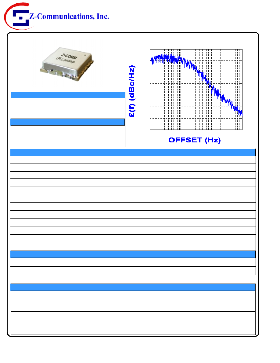
PHASE NOISE (1 Hz BW, typical)
LOW COST - HIGH PERFORMANCE
© Z-Communications, Inc.
All rights reserved
Page 1
PHASE LOCKED LOOP
FEATURES
APPLICATIONS
PERFORMANCE SPECIFICATIONS
VALUE
UNITS
POWER SUPPLY REQUIREMENTS
APPLICATION NOTES
163.84
MHz
∑
Step Size:
80 KHz
- Style Package
cPLL
∑
∑
∑
∑
A1
Rev
∑
AN-107 : How to Solder Z-COMM VCOs / PLLs
∑
AN-200 : Mounting and Grounding of Z-COMM PLLs
∑
AN-201 : PLL Fundamentals AN-202 : PLL Functional Description
NOTES:
Reference Oscillator Signal: 5 MHz<
f
osc
<100 MHz
Frequency Synthesizer: Analog Devices - ADF4001
9939 Via Pasar ∑ San Diego, CA 92126
TEL (858) 621-2700 FAX (858) 621-2722
Power Output
0±2
dBm
Load Impedance
50
Step Size
80
KHz
1250
163.84
-
∑ Frequency Range:
-
163.84
Charge Pump Output Current
µ
LOW COST - HIGH PERFORMANCE
PHASE LOCKED LOOP
© Z-Communications, Inc.
Page 2
Printed in the U.S.A.
PCA0163A
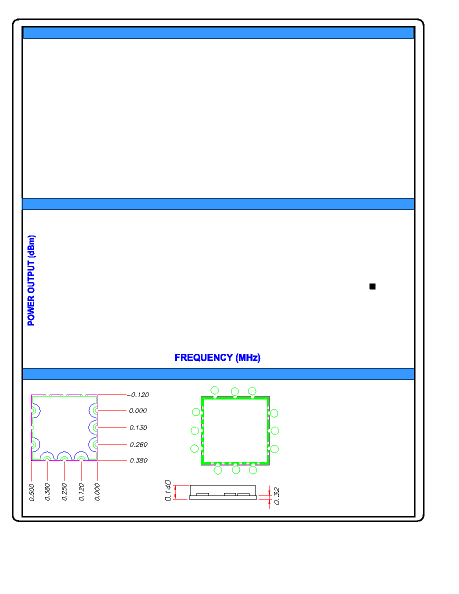
POWER CURVE, typ.
PAGE 2
PHYSICAL DIMENSIONS
SIDE VIEW
Bottom
View
2
1
12
3
4
5
6
7
8
9
10
11
Top View
P1 RF OUTPUT
P2 REFERENCE OSCILLATOR INPUT
P3 CLOCK
P4 DATA
P5 LOAD ENABLE
P6 LOCK DETECT
P7 VCC
P8 GROUND
P9 NO CONNECTION
P10-12 GROUND
1. The inside radius of all 14 half holes at the perimeter of the board
are plated to provide a surface for the attachment of the PLL Module
to the motherboard. 5 pads are for grounding, 8 pads are for signal
interface.
2. The surface of the shield is tin-plated and may be soldered to.
The shield's base metal is brass.
3.The ground plane on the bottom side is ground and attaches to a
ground track on the top side of the board as well as to the shield.
4. Unless otherwise noted all dimensions are in inches.
5.Unless otherwise noted all tolerances are as follows:
.xxx = ± .010
∞c
25
PLL OUTPUT SPECTRUM
FREQUENCY OFFSET (KHz)
POWER