- 1 -
ZEN2011P
P ROGRAMMABLE U N IVE RSAL COU N TE R
Description
is a 24 bit pr ogr a m m a ble u n iver sa l cou n t er LSI.
ZENIC INC. ZEN2011P
TH E
cou n t s ph a se-sh ift ed sign a ls a n d u p/down pu lse sign a ls, gen er a t ed fr om r ot a r y en coder s or lin ea r
ZEN2011P
sca les.
Sin ce t h e cou n t er r espon se speed is a s h igh a s 8MH z(MAX),t h e
is u sed in a va r iet y of h igh speed
ZEN2011P
ser vices in clu din g digit a l ser vo con t r ol a n d pr ecision m ea su r em en t .
TH E
is pr ovided wit h a fu n ct ion wh ich m on it or s in pu t sign a ls a n d det ect s a n y a bn or m a l in pu t
ZEN2011P
a ccom pa n ied wit h n oise or ot h er dist u r ba n ces, so t h a t t h e r elia bilit y of cou n t ed va lu es a r e secu r ed.
1, Features
24bit bin a r y u p/down cou n t er .
Cou n t er r espon se speed:
8MH z.(MAX) ( CLK f = 8MH z a t 50% du t y)
0
In pu t fr equ en cy of cou n t pu lse.
Two ph a se-sh ift ed pu lses sign a l in pu t :
A/B ph a se in pu t DC ~ 2MH z.
(less t h a n f
1/4)
0
~
U p/down pu lse sign a l in pu t :
U p/down in pu t DC ~ 4MH z
(less t h a n f
1/2)
0
~
CLK fr equ en cy DC ~ 8MH z.
(MAX.: du t y r a t io 50%)
Dir ect ion r ecogn it ion for u p/down cou n t
Abn or m a l in pu t det ect ion cir cu it .
P r eloa d r egist er for t h e u p/down cou n t er .
La t ch r egist er for t h e u p/down cou n t er .
Refer en ce va lu e - cou n t va lu e coin ciden ce
det ect ion fu n ct ion .
On -ch ip st a t u s r egist er .
Cou n t er oper a t ion m ode.
Qu a d/dou ble/sin gle edge eva lu a t ion .
(for ph a se-sh ift ed sign a l a n d sin gle pu lse)
Cou n t dir ect ion select ion .
Cou n t er clea r con t r ol:syn ch r on ou s/
a syn ch r on ou s clea r .
Com m a n d m ode
Mode 0:
1 ch . r efer en ce va lu e - cou n t va lu e
coin ciden ce det ect ion fu n ct ion .
Mode 1:
Mode 0 in st r u ct ion set com pa t ible.
2 ch . r efer en ce va lu e - cou n t va lu e
coin ciden ce det ect ion fu n ct ion .
Logica l OR ou t pu t of ea ch coin ciden ce
det ect ion s a va ila ble.
In t er r u pt ou t pu t u n der som e con dit ion s
a va ila ble.
8 bit da t a bu s.
Low power CMOS t ech n ology.
TTL com pa t ible.
Sin gle 5V power su pply.
28 pin DIP .
Typical Applications
N C m a ch in e t ools
P r ecision posit ion er s
Robot a r m con t r oller s
Speed con t r oller s for r ot a t in g m a ch in es
E lect r on ic ga u ges
F r equ en cy cou n t er s
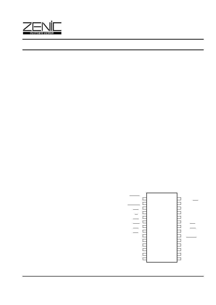
Pin configuration
(Top View)
E XTA
28
VDD
1
CLK
2
27
U D/AB
RE SE T
3
26
DIR
CE
4
25
SE L0
Z
C/D
5
24
SE L1
E
RD
6
23
SE L2
N
WR
7
22
A/U P
2
LD
8
21
B/DN
0
LT
9
20
Z/CLR
1
D0
10
19
E XTB
1
D1
11
18
D7
P
D2
12
17
D6
D3
13
16
D5
VSS
14
15
D4
ZENIC Inc.
- 2 -
ZEN2011P
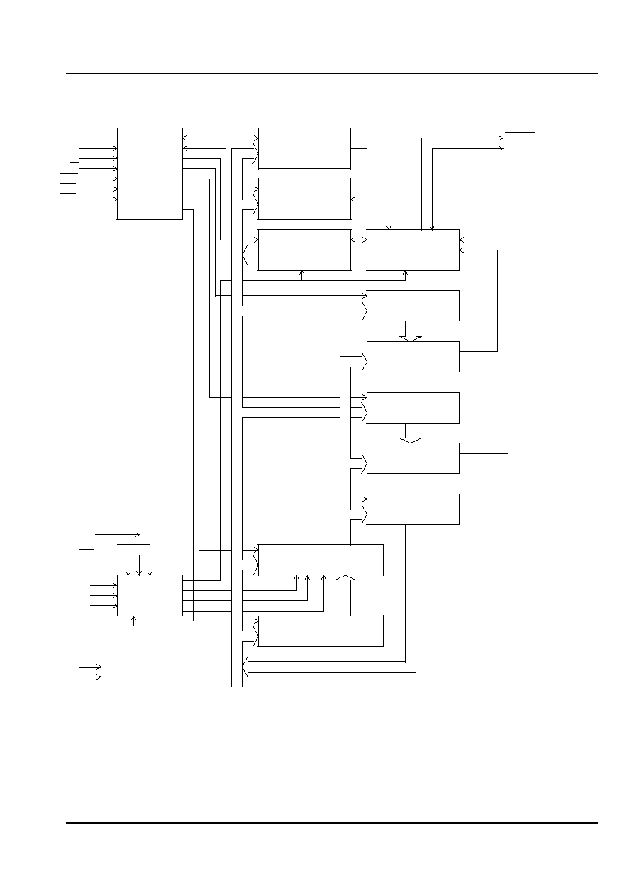
2, Block diagram
*
Mode 1
E XTA
LT
E XTB
Com m a n d r egist er
LD
Com m a n d
(8bit )
C/D
WR
decoder
RD
Mode 0
Com m a n d r egist er
CE
(8bit )
*
Mode 1
St a t u s r egist er
F u n ct ion
(8bit )
con t r ol
E QA
E QB
Refer en ce r eg. A
(24bit )
Com pa r a t or A
(24bit )
*
Refer en ce r eg. B
(24bit )
*
Com pa r a t or B
(24bit )
La t ch r egist er
(24bit )
RE SE T
SE L0
SE L2
~
U D/AB
U p/down cou n t er
DIR
(24bit )
AI
U P P U LSE
A/U P
Dir ect ion
DOWN P U LSE
B/DN
r ecogn it ion
COUN TE R CLE AR
Z/CLR
for u p/down
CLK
P r eloa d r egist er
(24bit )
VDD
VSS
D7~D0
N ot e:Block s m a r k ed(*) a r e va lid a t m ode 1
-
ZENIC Inc.

- 3 -
ZEN2011P
3, Pin Description
(1)
E XTA E xt er n a l A(Ou t pu t )
Th is ou t pu t depen ds on t h e com m a n d m ode.
In m ode 0, E XTA ou t pu t s t h e equ a l sign a l
(E QA).
In Mode 1, eit h er of da t a (E QA),
(E QA+E QB) or (IN TE QA) is select ed by t h e
com m a n d a n d it is ou t pu t .
Refer t o "5-3 Mode 1 com m a n d for m a t ".
(2)
CLK
Clock (In pu t :sin gle ph a se clock )
Th e CLK ser ves a s a clock in pu t solely t o
syn ch r on ize t h e in t er n a l cir cu it oper a t ion of
t h e
.
ZEN2011P
(3)
RE SE T Reset (In pu t )
Th e RE SE T in it ia lizes t h e u p/down cou n t er ,
ph a se discr im in a t ion cir cu it , com m a n d
r egist er ,a n d st a t u s r egist er .
(4)
CE
Ch ip en a ble(In pu t )
A "Low" level a t t h is in pu t en a bles t h e
t o a ccept a com m a n d or a da t a
ZEN2011P
in pu t fr om t h e CP U du r in g a wr it e cycle,
or t o t r a n sm it a da t a t o t h e CP U du r in g
a r ea d cycle.
(5)
C/D
Com m a n d/da t a select (In pu t )
Th e C/D defin es t h e t ype of in for m a t ion
t r a n sfer per for m ed bet ween t h e CP U a n d
t h e
.
ZEN2011P
(6)
RD
Rea d st r obin g(In pu t )
Th e RD is a st r obin g sign a l for r ea din g
da t a fr om a n in t er n a l r egist er .
(7)
WR
Wr it e st r obin g(In pu t )
Th e WR is a st r obin g sign a l for wr it in g
da t a in t o a n in t er n a l r egist er .
(8)
LD
Da t a loa din g t o t h e cou n t er *(In pu t )
Th e LD collect ively t r a n sm it s t h e da t a
st or ed in t h e pr eloa d r egist er t o t h e
u p/down cou n t er .
(9)
LT
Cou n t da t a la t ch *(In pu t )
Th e LT collect ively st or es t h e da t a of
t h e u p/down cou n t er in t o t h e r ea din g
r egist er .
(10~13,15~18)
D0~
Da t a bu s(Bidir ect ion a l 3-st a t e)
D7
(19)
E XTB
E xt er n a l B (I/O)
Th e da t a set depen din g on t h e com m a n d is
in pu t or ou t pu t .
In m ode 0, E XTB is set a s u n iva r sa l in pu t
t er m in a l U a n d it is m on it or ed by t h e st a t u s
r egist er .
In Mode 1, E XTB is set a s a n ou t pu t t er m in a l,
eit h er of da t a (E QB), (INTAI)
or (IN TE QB)
is select ed by t h e com m a n d a n d it is ou t pu t .
Refer t o
"5-3. Mode 1 com m a n d for m a t ".
(20)
Z/CLR Cou n t er clea r *(In pu t )
Th e Z/CLR a ccept s r eset sign a l wh ich clea r s
t h e u p/down cou n t er da t a .
(21)
B/DN
Cou n t pu lse in pu t B or DN *(In pu t )
(22)
A/U P
Cou n t pu lse in pu t A or U P *(In pu t )
Th e B/DN a n d A/UP a ccept s cou n t pu lse
sign a ls for t h e 24 bit cou n t er .
(23~25)
SE L0~S E L2
Cou n t er m ode select (In pu t )
Th e con dit ion s of t h ese pin s defin e t h e
cou n t er oper a t ion m ode t o sin gle ph a se or t o
du a l ph a se.
Th is defin it ion is effect ive wh en U D/AB
="Low".
(26)
DIR
Cou n t er dir ect ion select (In pu t )
Th e DIR select s t h e cou n t dir ect ion of t h e
u p/down cou n t er .
(27)
U D/AB U p/down or du a l ph a se pu lse m ode select
(In pu t )
P lea se r efer t o t h e pa r a gr a ph of "4-3.
Select ion of cou n t er oper a t ion m ode".
(14)
VSS
Gr ou n d(0v)
(28)
VDD
Su pply volt a ge(+5v)
N ot e: Sign a ls wit h (*)m a r k a r e sa m pled by CLK.
Sa m pled a t t h e r isin g edge of CLK:
Z/CLR,B/DN ,A/U P
Sa m pled a t t h e fa ilin g edge of CLK:
LD,LT.
ZENIC Inc.
- 4 -
ZEN2011P
4, Operation
Th e oper a t ion of
is con t r olled wit h t h e
ZEN2011P
syst em soft wa r e. To u se t h is cou n t er , it is n ecessa r y
t o
specify
"com m a n d
wor ds",
"cou n t er
r efer en ce
va lu e",a n d "cou n t ed va lu e" in a dva n ce.
Sin ce t h e t im in g is syn ch r on ized wh ich t r a n sfer da t a
bet ween t h e u p/down cou n t er a n d ot h er r egist er s, t h e
da t a r ea d/wr it e, com m a n d wr it e, a n d st a t u s r ea d ca n
be ca r r ied ou t even wh en t h e cou n t er is oper a t in g.
4-1.Command mode
In
, t wo k in ds of syst em m ode descr ibed in
ZEN2011P
t h e followin g ca n be select ed.
F ir st of a ll, it is n ecessa r y t o select eit h er of syst em
m ode by t h e com m a n d in in it ia liza t ion . N ext , it is
n ecessa r y t o specify a com m a n d wor d, a cou n t er
va lu e, a n d a va lu e of ea ch r egist er n ecessa r y for
in it ia lizin g t h e cou n t oper a t ion befor eh a n d.
(1) Mode 0
Aft er com m a n d:90H is execu t ed
(
)
or syst em r eset
E XTB (pin N o.19) is set a s u n iver sa l in pu t
t er m in a l U.
Th e r efer en ce r egist er -A a n d t h e com pa r a t or -A
becom e effect ive.
)
(2) Mode 1
( Aft er com m a n d:91H is execu t ed
In t h is m ode it is a va ila ble a s for a ll in st r u ct ion
set s of m ode 0.
E XTB (pin N o.19) is set in t h e ou t pu t t er m in a l.
Mor eover , E XTA (pin N o.1) a n d E XTB (pin
N o.19) ca n con t r ol t h e ou t pu t da t a by t h e
in st r u ct ion set of Mode 1.
Mor eover , t h e r efer en ce r egist er -B a n d t h e
com pa r a t or -B becom e effect ive.
4-2.Read/write logic
Th e r ea d or wr it e oper a t ion of t h e
is
ZEN2011P
select ed u sin g fou r sign a ls, CE , C/D, RD, a n d WR.
Det a il of t h e select ion is sh own in Ta b.1.
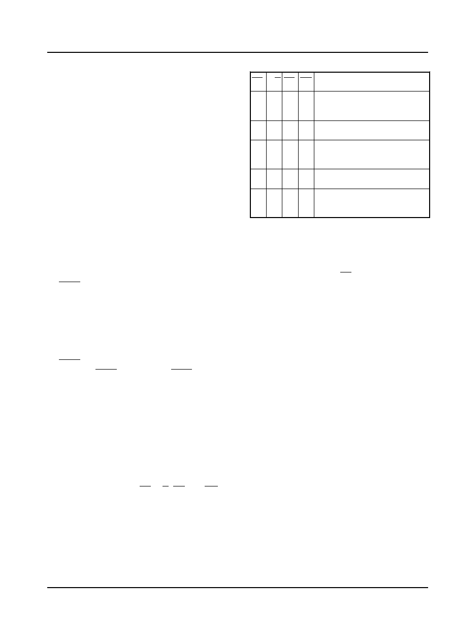
Tab.1 The read/write operation
Oper a t ion
CE
C/D RD WR
H
X
X
X
Disa ble(da t a bu s is a t h igh
im peda n ce con dit ion )
L
L
L
H
Da t a r ea d(la t ch r egist er )
L
L
H
L
Da t a wr it e(pr eloa d,r efer en ce
r egist er , u p/down cou n t er )
L
H
L
H
St a t u s r ea d(st a t u s r egist er )
L
H
H
L
Com m a n d wr it e(com m a n d
r egist er )
4-3.Selection of counter operation mode
Th e
sa m ples t h e cou n t in pu t s u sin g t h e
ZEN2011P
CLK.
U sin g fou r sign a ls of U D/AB a n d SE L0 SE L2, t h e
~
t ype of cou n t er pu lse in pu t a n d t h e t ype of
cou n t er
clea r ca n be select ed. Refer t o Ta b.2
for det a il.
Th e cou n t in g oper a t ion s a r e ca r r ied ou t by sa m plin g
t h e con dit ion s of A,B,a n d Z a t t h e r isin g edge of CLK.
ZENIC Inc.
- 5 -
ZEN2011P
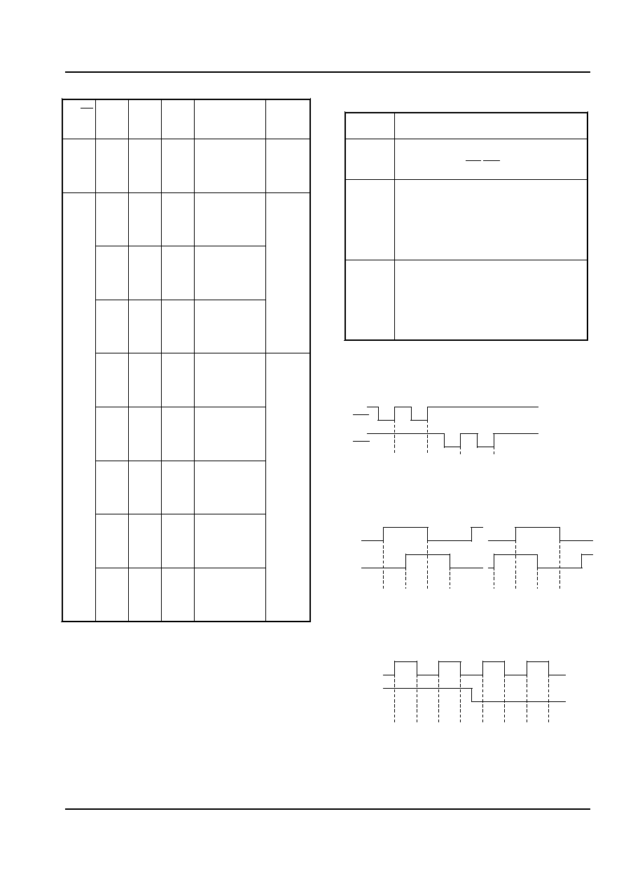
Tab.2 Counting mode selection
SE L2 SE L1 SE L0
P u lse in pu t
Clea r
U D/AB
(E dge eva l.)
m ode
H
X
X
X
U p/Down
Asyn ch -
pu lse
r on ou s
clea r
P h a se-
L
L
L
sh ift ed
(Sin gle)
P h a se-
Syn ch r o
L
L
H
sh ift ed
-n ou s
(Dou ble)
clea r
m ode
P h a se-
L
H
L
sh ift ed
(Qu a d)
P h a se-
H
L
L
sh ift ed
(Sin gle)
L
P h a se-
H
L
H
sh ift ed
(Dou ble)
P h a se-
Asyn ch -
H
H
L
sh ift ed
r on ou s
(Qu a d)
clea r
m ode
Sin gle pu lse
L
H
H
(S in gle)
Sin gle pu lse
H
H
H
(Dou ble)
4-4.Count operation with pulse input
P u lse
Cou n t oper a t ion
U p/down
pu lse
At t h e r isin g U P ,DN pu lse.
At t h e ph a se ch a n ge of A,B pu lse
P h a se-
Sin gle:Ch a n ge of ph a se A
sh ift ed
(on ly wh en ph a se B is "L")
Dou ble:Ch a n ge of ph a se A
Qu a d
:Ch a n ge of ph a se A,B
Cou n t u p wit h pu lse A, a s cou n t
Sin gle
en a ble sign a l wit h B.
pu lse Sin gle:Ch a n ge of ph a se A
(on ly a t t h e r isin g pu lse)
Dou ble:Ch a n ge of ph a se A
Edge evaluation ( 1:count
0:not count )
Up/down pulse input
U P
DN
1
1
1
1
N ot e: Bot h u p/down pu lse sh ou ld n ot be
sim u lt a n eou sly set t o a "Low" level.
Phase-shifted pulse input
A
B
Sin gle
1
0
0
0
0
0
0
1
Dou ble 1
0
1
0
0
1
0
1
Qu a d
1
1
1
1
1
1
1
1
Single pulse input
A
B
Sin gle
1
0
1
0
0
0
0
0
Dou ble
1
1
1
1
0
0
0
0
N ot e: B is u sed for a cou n t en a ble sign a l.
ZENIC Inc.