
- 1 -
ZEN2041F
P ROGRAMMABLE U N IVE RSAL COU N TE R
Description
is a pr ogr a m m a ble u n iver sa l cou n t er LSI.
ZENIC ZEN2041F
TH E
cou n t s ph a se-sh ift ed sign a ls a n d u p/down pu lse sign a ls, gen er a t ed fr om r ot a r y en coder s or
ZEN2041F
lin ea r sca les.
Sin ce t h e cou n t er r espon se speed is a s h igh a s 20MH z(MAX),t h e
is u sed in a va r iet y of h igh speed
ZEN2041F
ser vices in clu din g digit a l ser vo con t r ol a n d pr ecision m ea su r em en t .
TH E
is pr ovided wit h a fu n ct ion wh ich m on it or s t h e in pu t sign a ls a n d det ect s a n y a bn or m a l in pu t
ZEN2041F
a ccom pa n ied wit h n oise or ot h er dist u r ba n ces, so t h a t t h e r elia bilit y of cou n t ed va lu es a r e secu r ed.
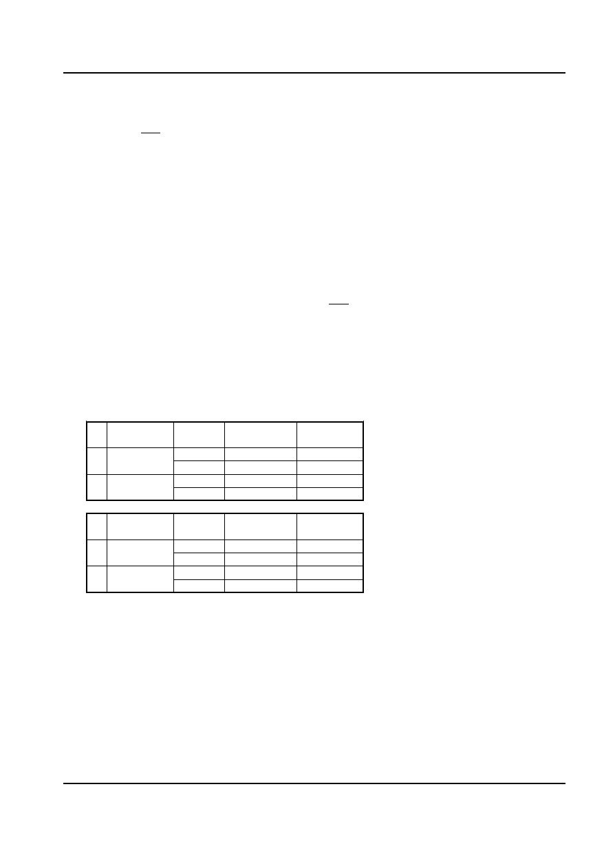
1. Features
Select a ble cou n t r esolu t ion a n d ch a n n els.
16bit
4ch . or 32bit
2ch . or
16bit
2ch .
32bit
1ch .
+
Cou n t r espon se speed:
20Mcps.(MAX.) ( CLK f = 20MH z a t 50% du t y)
0
In pu t fr equ en cy of cou n t pu lse.
P h a se sh ift ed sign a l in pu t :
-
A/B ph a se in pu t DC
5MH z.
~
(less t h a n f
1/4)
0
U p/down pu lse sign a l in pu t :
U p/down in pu t DC
10MH z
~
(less t h a n f
1/2)
0
CLK fr equ en cy DC
20MH z.
~
(MAX.:du t y r a t io 50%)
Dir ect ion r ecogn it ion for u p/down cou n t in g
Abn or m a l in pu t det ect ion cir cu it .
P r eloa d r egist er for t h e u p/down cou n t er .
La t ch r egist er for t h e u p/down cou n t er .
Refer en ce va lu e cou n t va lu e coin ciden ce
-
det ect ion fu n ct ion .
On ch ip st a t u s r egist er .
-
Cou n t er oper a t ion m ode.
E dge eva lu a t ion select ion : 1/2/4 .
(on ly for ph a se sh ift ed sign a l in pu t )
-
Cou n t dir ect ion select ion .
Cou n t er clea r con t r ol:syn ch r on ou s/
a syn ch r on ou s clea r .
Select a ble 16/8 bit da t a bu s.
Low power CMOS t ech n ology.
TTL com pa t ible.
Sin gle 5V power su pply.
100 pin QF P .
Typical Applications
F or Mu lt i ch a n n el
N C m a ch in e t ools
P r ecision posit ion er s
Robot a r m con t r oller s
Speed con t r oller s for r ot a t in g m a ch in es
E lect r on ic ga u ges
F r equ en cy cou n t er s
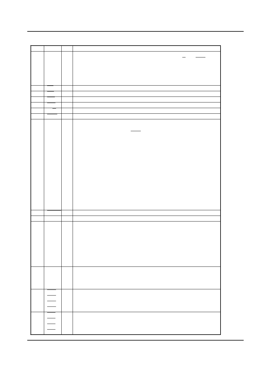
Pin configuration
Top View)
(
ZENIC Inc.
(Z2041B98)
P0
1
P0
0
VS
S
VDD
E
00/
O
0
0
E
01/
O
0
1
EP
0
/
O
0
2
VS
S
IN
T
RE
S
E
T
W
/B
BH
E
RD
W
R
CS
D0
D1
D2
D3
VDD
D4
D5
D6
D7
VDD
VDD
VS
S
VS
S
CL
K
1
2
3
4
5
6
7
8
9
10
11
12
13
14
15
16
17
18
19
20
21
22
23
24
25
26
27
28
29
30
3 1
3 2
3 3
3 4
3 5
3 6
3 7
3 8
3 9
4 0
4 1
4 2
4 3
4 4
4 5
4 6
4 7
4 8
4 9
5 0
AD0
AD1
AD2
AD3
AD4
AD5
D8
D9
D1 0
VDD
VSS
D1 1
D1 2
D1 3
D1 4
D1 5
DI R2
MD2
1 0 0
9 9
9 8
9 7
9 6
9 5
9 4
9 3
9 2
9 1
9 0
8 9
8 8
8 7
8 6
8 5
8 4
8 3
8 2
8 180
79
78
77
76
75
74
73
72
71
70
69
68
67
66
65
64
63
62
61
60
59
58
57
56
55
54
53
52
51
VS
S
VS
S
VDD
VDD
EP
3
/
O
3
2
E3
1
/
O
3
1
E3
0
/
O
3
0
VDD
P3
0
P3
1
C3
LD
3
LT3
M
D3
DI
R
3
S1
LD
2
LT2
VS
S
E2
0
/
O
2
0
E2
1
/
O
2
1
EP
2
/
O
2
2
C2
VDD
VS
S
P2
1
P2
0
LT1
LD1
DI R1
MD1
EP1 / O1 2
VDD
P1 0
P1 1
C1
S0
LT0
LD0
DI R0
MD0
C0
N.C.
N . C .
N . C .
N.C
.
N.C
.
N.C.
N . C .
E 1 1 / O 1 1
E 1 0 / O 1 0
V S S
N . C .

- 2 -
ZEN2041F
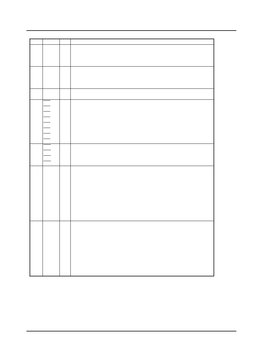
2. Block diagram (Figure.2)
AD5-0
CS
WR
CP U
Da t a bu s
RD
In t er fa ce
bu ffer
D15-D0
IN T
BH E
W/B
Con t r ol logic
Com pa r a t or
P 00
Gr ou p
Cou n t er
P 01
0
u n it 0
0
E 00/O00
CM
CMR
C0
Dir ec-
LDR
CNT
LTR
R
LD0
t ion
0
0
0
E 01/O01
00
01
LT0
r ecog-
MD0
n it ion
E P 0/O02
DIR0
Com pa r a t or
P 10
Gr ou p
Cou n t er
P 11
1
u n it 1
1
E 10/O10
CMR
CMR
C1
Dir ec-
LDR
CNT
LTR
LD1
t ion
1
1
1
E 11/O11
10
11
LT1
r ecog-
MD1
n it ion
E P 1/O12
DIR1
S0
Com pa r a t or
P 20
Gr ou p
Cou n t er
P 21
2
u n it 2
2
E 20/O20
CMR
CMR
C2
Dir ec-
LDR
CNT
LTR
LD2
t ion
2
2
2
E 21/O21
20
21
LT2
r ecog-
MD2
n it ion
E P 2/O22
DIR2
Com pa r a t or
P 30
Gr ou p
Cou n t er
P 31
3
u n it 3
2
E 30/O30
CMR
CMR
C3
Dir ec-
LDR
CNT
LTR
LD3
t ion
3
3
3
E 31/O31
30
31
LT3
r ecog-
MD3
n it ion
E P 3/O32
DIR3
S1
RE SE T
LDR
:P r eloa d Regist er
CLK
CN T
:U p/down Cou n t er
VDD
LTR
:La t ch Regist er
VSS
CMR
:Refer en ce Regist er
ZENIC Inc.
(Z2041B98)
- 3 -
ZEN2041F
3. Block Description (refer to Figure.2)
1) CP U In t er fa ce
It is in t er fa ce t o wr it e da t a in t o r egist er or r ea d da t a fr om r egist er .
It ou t pu t s t h e IN T sign a l by in t er r u pt fr om dir ect ion r ecogn it ion logic a n d com pa r a t or .
Refer t o [5.Ba sic Oper a t ion s] a n d [6.In t er n a l Regist er Ma ppin g].
2) Con t r ol logic
It oper a t es t o wr it e da t a in t o r egist er or r ea d da t a fr om r egist er .
It t r a n sm it s in t er r u pt sign a l t o CP U in t er fa ce fr om dir ect ion r ecogn it ion logic a n d com pa r a t or .
3) Da t a Bu s Bu ffer
It is 16 or 8bit bidir ect ion a l, a n d in t er fa ce bet ween CP U a n d
.
ZEN2041F
4) Dir ect ion Recogn it ion
It ou t pu t s t h e U P , DOWN , Da t a Loa d a n d Da t a La t ch sign a l t o t h e cou n t er u pon t h e ext er n a l sign a l, m ode
r egist er , com m a n d r egist er .
If in t er r u pt en a ble, it in dica t es CP U in t er fa ce t o m a k e IN T="L".
Th e in pu t sign a ls ca n be m on it or ed by t h e m on it or r egist er , t h er efor e t h e in pu t sign a ls(*) n ot in pu t ed t o
t h e cou n t er ca n be u sed for u n iver sa l in pu t s.
5) Cou n t er u n it
It is com posed of t h e loa d r egist er , u p/down cou n t er a n d com m a n d r egist er .
It oper a t es by t h e U P , DOWN , CLE AR, DATA LOAD, DATA LATCH , a n d Ca r r y, Bor r ow.
Th e cou n t er con n ect ion S0 a n d S1 det er m in e t h e dir ect ion r ecogn it ion gr ou p a n d t h e pr e-st a ge cou n t er .
S0
Con n ect ion
Cou n t er
Dir ect ion
P r e-st a ge
u n it
Recogn it ion
Cou n t er u n it
0
In depen den t
0
Gr ou p 0
-
1
1
-
1
Ca sca de
0
0
-
1
0
0
S1
Con n ect ion
Cou n t er
Dir ect ion
P r e-st a ge
u n it
Recogn it ion
Cou n t er u n it
0
In depen den t
2
Gr ou p 2
-
3
3
-
1
Ca sca de
2
2
-
3
2
2
Ca sca de con n ect ion ( 32bit cou n t er )
Cou n t er u n it 0 a n d 2 a r e lower wor d(16bit ).
An d, cou n t er u n it 1 a n d 3 a r e u pper wor d(16bit ).
6) Com pa r a t or
It is com posed of t wo r efer en ce r egist er s.
It com pa r es t h e cou n t er va lu e wit h t h e r efer en ce r egist er . If t h e coin ciden ce is det ect ed, com pa r a t or
ou t pu t s t h e st a t u s, t h e in t er r u pt , t h e coin ciden ce a n d t h e win dow, a ccor din g t o t h e set t in g con dit ion .
Refer t o [9.Coin ciden ce Det ect ion F u n ct ion ].
*)In pu t sign a ls t o t h e gr ou p 1 a n d 3 wh en ca sca de con n ect ed.
ZENIC Inc.
(Z2041B98)
- 4 -
ZEN2041F
4. Pin Definitions and Functions
Ta ble.1
P in
Sym bol I/O
F u n ct ion s
36
AD5
Addr ess0-5
35
AD4
Th ese a r e u sed for select ion in t er n a l r egist er wit h W/B a n d BH E .
34
AD3
I
Refer t o [5.Ba sic Oper a t ion s] a n d [6.In t er n a l Regist er Ma ppin g].
33
AD2
32
AD1
31
AD0
16
CS
I
CH IP SE LE CT
14
RD
I
RE AD
15
WR
I
WRITE
10
IN T
O
IN E RRU P T RE QU E ST
12
W/B
I
WORD/BYTE : Wor d t r a n sfer is "H ". Byt e t r a n sfer is "L".
13
BH E
I
BU S H IGH E N ABLE
46
D15
DATA BUS
45
D14
44
D13
E n a ble bit s a r e select ed by BH E a n d AD0.
43
D12
Refer t o [5.Ba sic Oper a t ion s.].
42
D11
39
D10
38
D9
37
D8
I/O
25
D7
24
D6
23
D5
22
D4
20
D3
19
D2
18
D1
17
D0
11
I
RE SE T:in it ia lize in t er n a l r egist er s.
RESET
30
CLK
I
CLOCK:is u sed for syn ch r on izin g in t er n a l sign a ls a n d cou n t in g.
2
P 00
P U LSE IN P U TS 00-31
1
P 01
Refer t o [8. Cou n t er Oper a t ion a n d Tim in g.].
91
P 10
92
P 11
I
51
P 20
52
P 21
70
P 30
69
P 31
100
C0
CLE AR0-3 : clea r ea ch cou n t er va lu e.
93
C1
I
Abou t clea r con dit ion s, r efer t o [7.5) Mode Regist er .].
55
C2
68
C3
97
LD0
DATA LOAD : Aft er t h e fa llin g edge is det ect ed, t h e va lu e of loa d
83
LD1
I
r egist er is st or ed t o ea ch cou n t er .
61
LD2
67
LD3
96
LT0
DATA LATCH : Aft er t h e fa llin g edge is det ect ed, t h e va lu e of cou n t er
82
LT1
I
is st or ed t o ea ch la t ch r egist er .
60
LT2
66
LT3
ZENIC Inc.
(Z2041B98)
- 5 -
ZEN2041F
P in
Sym bol I/O
F u n ct ion s
99
MD0
MODE SE LE CTION :
85
MD1
I
O : P h a se-sh ift ed pu lse
50
MD2
1 : U p/Down pu lse
65
MD3
98
DIR0
COU N TIN G DIRE CTION
84
DIR1
I
Refer t o [8. Cou n t in g Oper a t ion a n d Tim in g.].
49
DIR2
64
DIR3
94
S0
I
COU N TE R CON N E CTION
63
S1
Refer t o [3.5) Cou n t er u n it ].
5
COIN CIDE N CE DE TE CTION 00-31 / U N IVE RSAL OU TP U T 00-31
E00/O00
6
Refer t o [9. Coin ciden ce Det ect ion F u n ct ion .].
E01/O01
E20/O20
58
57
O
E21/O21
E10/O10
88
E11/O11
87
E30/O30
72
E31/O31
73
7
WIN DOW OU TP U T 0-3 / U NIVE RSAL OU TP U T 02-32
EP0/O02
86
O
Refer t o [9. Coin ciden ce Det ect ion F u n ct ion .].
EP1/O12
EP2/O22
56
EP3/O32
74
4
Su pply volt a ge +5V
21
26
27
40
54
VDD
-
71
76
77
90
3
Gr ou n d 0V
9
28
29
41
53
VSS
-
59
78
79
89
ZENIC Inc.
(Z2041B98)