
SOT23 SILICON HIGH
SPEED SWITCHING DIODE
ISSUE 2 JANUARY 1995
PIN CONFIGURATION
PARTMARKING DETAILS
BAS19 A8
BAS20 A81
BAS21 A82
ABSOLUTE MAXIMUM RATINGS.
PARAMETER
SYMBOL
BAS19
BAS20
BAS21
UNIT
Continuous Reverse Voltage
V
R
100
150
200
V
Repetative Peak Reverse Voltage
V
RRM
120
200
250
V
Average Forward Rectified Current
I
F(AV)
200
mA
Forward Current
I
F
200
mA
Repetative Peak Forward Current
I
FRM
625
mA
Power Dissipation at T
amb
=25∞C
P
tot
330
mW
Operating and Storage Temperature
Range
T
j
:T
stg
-55 to +150
∞C
ELECTRICAL CHARACTERISTICS (at T
amb
= 25∞C unless otherwise stated).
PARAMETER
SYMBOL MIN. TYP. MAX. UNIT CONDITIONS.
Reverse
Breakdown
Voltage
V
(BR)
BAS19
120
V
I
R
=100
µ
A (1)
BAS20
200
V
I
R
=100
µ
A (1)
BAS21
250
V
I
R
=100
µ
A (2)
Reverse Current
I
R
100
100
nA
µ
A
V
R
=V
R
max
V
R
=V
R
max, T
J
=150∞C
Static Forward Voltage V
F
1.00
1.25
IF=100mA
I
F
=200mA
Differential Resistance r
diff
5
I
F
=10mA
Diode Capacitance
C
d
5
pF
f=1MHz
Reverse Recovery Time t
rr
50
ns
I
F
=30mA to I
R
=30mA
R
L
=10
measured at I
R
=3mA
(1) Measured under pulsed conditions. Pulse width=300
µ
s. Duty cycle
2%
(2) At zero life time, measured under pulse conditions to avoid excessive dissipation and voltage
limited
to
275V
Spice parameter data is available upon request for this device
BAS19
BAS20
BAS21
PAGE NO
1
3
2
SOT23
BAS19
BAS20
BAS21
!
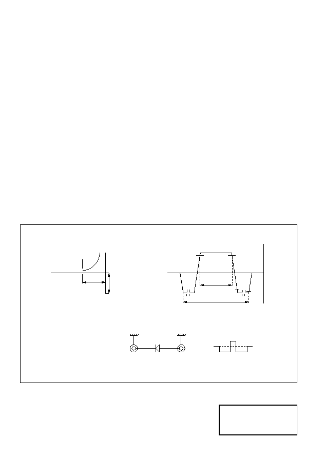
SWITCHING TIME TEST DATA
Sampling Oscilloscope
R
IN
=50
DUT
R
S
=50
Pulse Generator
t
rr
+I
F
t
I
R*
t
p(tot)
t
p
90%
10%
90%
V
Recovery Time Equivalent Test Circuit
Input Signal
Output Signal
Input Signal
Total Pulse Duration
t
p(tot)
2
µ
s
Duty Factor
0.0025
Rise Time of Reverse
Pulse
t
r
0.6ns
Reverse Pulse Duration
t
p
100ns
Oscilloscope
Rise Time
t
r
0.35ns
Circuit Capacitance*
C
<1pF
SOT23 SILICON HIGH
SPEED SWITCHING DIODE
ISSUE 2 JANUARY 1995
PIN CONFIGURATION
PARTMARKING DETAILS
BAS19 A8
BAS20 A81
BAS21 A82
ABSOLUTE MAXIMUM RATINGS.
PARAMETER
SYMBOL
BAS19
BAS20
BAS21
UNIT
Continuous Reverse Voltage
V
R
100
150
200
V
Repetative Peak Reverse Voltage
V
RRM
120
200
250
V
Average Forward Rectified Current
I
F(AV)
200
mA
Forward Current
I
F
200
mA
Repetative Peak Forward Current
I
FRM
625
mA
Power Dissipation at T
amb
=25∞C
P
tot
330
mW
Operating and Storage Temperature
Range
T
j
:T
stg
-55 to +150
∞C
ELECTRICAL CHARACTERISTICS (at T
amb
= 25∞C unless otherwise stated).
PARAMETER
SYMBOL MIN. TYP. MAX. UNIT CONDITIONS.
Reverse
Breakdown
Voltage
V
(BR)
BAS19
120
V
I
R
=100
µ
A (1)
BAS20
200
V
I
R
=100
µ
A (1)
BAS21
250
V
I
R
=100
µ
A (2)
Reverse Current
I
R
100
100
nA
µ
A
V
R
=V
R
max
V
R
=V
R
max, T
J
=150∞C
Static Forward Voltage V
F
1.00
1.25
IF=100mA
I
F
=200mA
Differential Resistance r
diff
5
I
F
=10mA
Diode Capacitance
C
d
5
pF
f=1MHz
Reverse Recovery Time t
rr
50
ns
I
F
=30mA to I
R
=30mA
R
L
=10
measured at I
R
=3mA
(1) Measured under pulsed conditions. Pulse width=300
µ
s. Duty cycle
2%
(2) At zero life time, measured under pulse conditions to avoid excessive dissipation and voltage
limited
to
275V
Spice parameter data is available upon request for this device
BAS19
BAS20
BAS21
PAGE NO
1
3
2
SOT23
BAS19
BAS20
BAS21
!
SWITCHING TIME TEST DATA
Sampling Oscilloscope
R
IN
=50
DUT
R
S
=50
Pulse Generator
t
rr
+I
F
t
I
R*
t
p(tot)
t
p
90%
10%
90%
V
Recovery Time Equivalent Test Circuit
Input Signal
Output Signal
Input Signal
Total Pulse Duration
t
p(tot)
2
µ
s
Duty Factor
0.0025
Rise Time of Reverse
Pulse
t
r
0.6ns
Reverse Pulse Duration
t
p
100ns
Oscilloscope
Rise Time
t
r
0.35ns
Circuit Capacitance*
C
<1pF