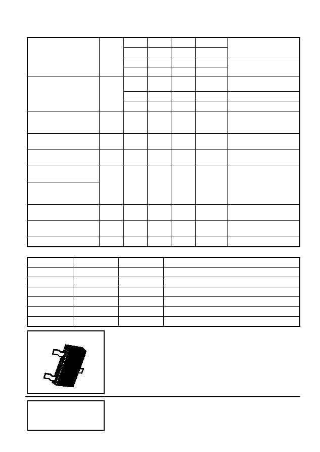
SOT23 P-CHANNEL ENHANCEMENT
MODE VERTICAL DMOS FET
ISSUE 2 SEPTEMBER 1995 7
PARTMARKING DETAIL
SP
ABSOLUTE MAXIMUM RATINGS.
PARAMETER
SYMBOL
VALUE
UNIT
Drain-Source Voltage
V
DS
-50
V
Continuous Drain Current
I
D
-130
mA
Pulsed Drain Current
I
DM
-520
mA
Gate-Source Voltage Peak
V
GS
±
20
V
Power Dissipation at T
amb
=25∞C
P
TOT
360
mW
Operating and Storage Temperature Range
t
j
:t
stg
-55 to +150
∞C
ELECTRICAL CHARACTERISTICS (at T
amb
= 25∞C).
PARAMETER
SYMBOL MIN.
TYP.
MAX. UNIT
CONDITIONS.
Drain-Source
Breakdown Voltage
BV
DSS
-50
V
V
GS
=0V, I
D
=0.25mA
Gate-Source
Threashold Voltage
V
GS(th)
-0.8
-1.5
-2.0
V
V
DS
=V
GS
, I
D
=-1mA
Zero gate Voltage
Drain Current
I
DSS
-1
-2
-15
-60
-100
µ
A
µ
A
T
j
=25 ∞C
T
j
=125 ∞C
V
DS
=-50V, V
GS
=0V(2
)
T
j
=25
∞
C
V
DS
=-25V, V
GS
=0V
Gate-Source Leakage
Current
I
GSS
-1
-10
nA
V
GS
=
±
20V
V
DS
=0V
Drain Source On-State
Resistance (1)
R
DS(on)
6
10
V
GS
=-5V
I
D
=-100mA
Forward
Transconductance (1)
(2)
g
fs
0.05
0.07
S
V
DS
=-25V
I
D
=-100mA
Input Capacitance (2)
C
iss
40
pF
V
GS
=0V
V
DS
=-25V
f=1MHz
Output Capacitance
C
oss
15
Reverse Transfer
Capacitance (2)
C
rss
6
Turn-On Time t
on
td(on)
10
ns
V
DD
=-30V
I
D
=-0.27A
V
GS
=-10V
R
GS
=50
t
r
10
Turn-Off Time t
off
t
d(off)
18
t
f
25
* (1) Measured under pulsed conditions. Pulse width = 300
µ
s. Duty cycle 2%
(2) Sample test.
BSS84
D
G
S
3 - 69