 | –≠–ª–µ–∫—Ç—Ä–æ–Ω–Ω—ã–π –∫–æ–º–ø–æ–Ω–µ–Ω—Ç: FCX705TA | –°–∫–∞—á–∞—Ç—å:  PDF PDF  ZIP ZIP |
FCX705
ISSUE 2 - AUGUST 2001
120V NPN SILICON HIGH VOLTAGE DARLINGTON TRANSISTOR
SUMMARY
DESCRIPTION
This new NPN Darlington transistor provides users with very efficeint
performance combining low V
CE
(sat) and very high Hfe to give extremely low
on state losses at 120V operation. This makes it deal for use in a variety of
efficient driving functions including motors, lamps relays and solenoids and
will also benefit circuits requiring high output current switching.
FEATURES
∑
Low Saturation Voltage
∑
Hfe min 3K @ 1A
∑
I
C
= -2A Continuous
∑
SOT89 package with Ptot - 1W
∑
Specification is also available in Eline and SOT223 package outlines
APPLICATIONS
∑
Various driving functions
- Lamps
- Motors
- Relays and solenoids
∑
High output current switches
ORDERING INFORMATION
DEVICE
REEL SIZE
(inches)
TAPE WIDTH
(mm)
QUANTITY
PER REEL
FCX705TA
7
12mm embossed
1000 units
DEVICE MARKING
705
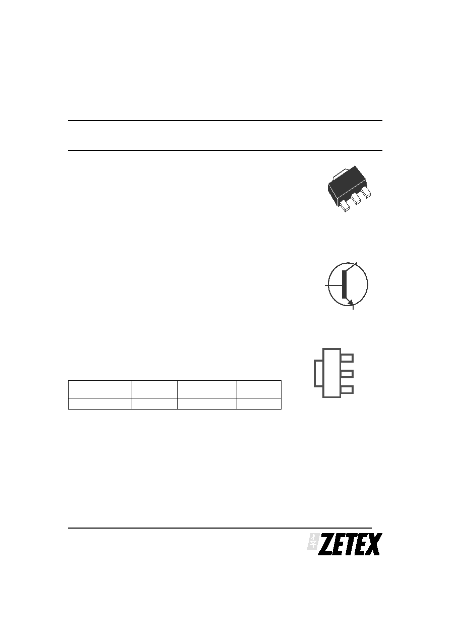
Top View
1
SOT 89
B
C
E
V
CEO
=120V; V
CE(sat)
= 1.3V; I
C
= 1A
C
B
C
E
ISSUE 2 - AUGUST 2001
FCX705
THERMAL RESISTANCE
PARAMETER
SYMBOL
VALUE
UNIT
Junction to Ambient (a)
R
JA
125
∞C/W
Junction to Ambient (b)
R
JA
45
∞C/W
NOTES
(a) For a device surface mounted on 25mm x 25mm FR4 PCB with high coverage of single sided 1oz copper,
in still air conditions
(b) For a device surface mounted on FR4 PCB measured at t 5 secs.
2
ABSOLUTE MAXIMUM RATINGS.
PARAMETER
SYMBOL
LIMIT NPN
UNIT
Collector-Base Voltage
V
CBO
-140
V
Collector-Emitter Voltage
V
CEO
-120
V
Emitter-Base Voltage
V
EBO
-10
V
Peak Pulse Current
I
CM
-4
A
Continuous Collector Current
I
C
-1
A
Power Dissipation at TA=25∞C (a)
Linear Derating Factor
P
D
1
8
W
mW/∞C
Power Dissipation at TA=25∞C (b)
Linear Derating Factor
P
D
2.8
22
W
mW/∞C
Operating and Storage Temperature Range
T
j
:T
stg
-55 to +150
∞C
ISSUE 2 - AUGUST 2001
FCX705
ELECTRICAL CHARACTERISTICS (at T
amb
= 25∞C unless otherwise stated).
PARAMETER
SYMBOL
MIN.
TYP.
MAX.
UNIT
CONDITIONS.
Collector-Base Breakdown
Voltage
V
(BR)CBO
-140
V
I
C
= -100 A
Collector-Emitter Breakdown
Voltage
V
(BR)CEO
-120
V
I
C
= -10mA*
Emitter-Base Breakdown Voltage
V
(BR)EBO
-10
V
I
E
= -100 A
Collector Cut-Off Current
I
CBO
-100
-10
nA
µA
V
CB
= -10V
V
CB
= -120V
Tamb = 100∞C
Emitter Cut-Off Current
I
EBO
-0.1
µA
V
EB
= -8V
Collector Emitter Cut-Off Current
I
CES
-10
µA
V
CES
= -120V
Collector-Emitter Saturation
Voltage
V
CE(sat)
-1.3
-2.5
V
V
I
C
= -1A, I
B
= -1mA*
I
C
= -2A, I
B
= -2mA*
Base-Emitter Saturation Voltage
V
BE(sat)
-1.8
V
I
C
= -1A, I
B
= -1mA*
Base-Emitter Turn-On Voltage
V
BE(on)
-1.7
V
I
C
= -1A, V
CE
= -5V*
Static Forward Current Transfer
Ratio
h
FE
3K
3K
3K
2K
30K
I
C
= -50mA, V
CE
= -5V*
I
C
= -500mA, V
CE
= -5V*
I
C
= -1A, V
CE
= -5V*
I
C
= -2A, V
CE
= -5V*
Transition Frequency
f
T
160
MHz
I
C
= -100mA, V
CE
= -10V
f= 20MHz
Input Capacitance
C
ibo
90
pF
V
CB
= -500mV, f= 1MHz
Output Capacitance
C
obo
15
pF
V
CB
= -10V, f= 1MHz
Turn-On Time
t
(on)
0.6
µs
I
C
= -500mA, V
CE
= -10V
I
B1
=I
B2
= -0.5mA
Turn-Off Time
t
(off)
0.8
µs
I
C
= -500mA, V
CE
= -10V
I
B1
=I
B2
= -0.5mA
*Measured under pulsed conditions. Pulse width=300
µ
s. Duty cycle
2%
3
Nb. Spice parameter data is available upon request for this device.
ISSUE 2 - AUGUST 2001
FCX705
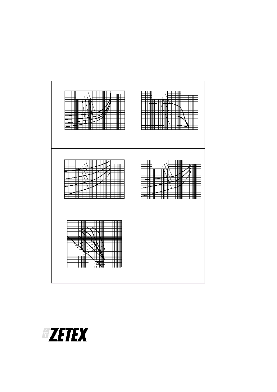
NPN TYPICAL CHARACTERISTICS
4
0.01
0.1
20
1
10
V
CE(sat)
v I
C
I
C
- Collector Current (Amps)
V
C
E
(s
at)
-
(
V
olts)
I
C
-
Collector
Current
(Amps)
V
CE
- Collector Voltage (Volts)
Safe Operating Area
100
1
10
0.1
1
10
Single Pulse Test at T
amb
=25∞C
D.C.
1s
100ms
10ms
1.0ms
0.1ms
0.001
0.01
0.1
20
1
10
10k
8k
6k
4k
0
2k
16k
14k
12k
+100∞C
+25∞C
-55∞C
I
C
- Collector Current (Amps)
h
FE
v I
C
h
FE
-
Gain
V
CE
=-5V
0.001
0.01
0.1
20
1
10
-55∞C
+25∞C
+100∞C
+175∞C
I
C
- Collector Current (Amps)
V
BE(sat)
v I
C
V
BE
(s
a
t
)
-(
V
olts)
I
C
/I
B
=1000
0.001
0.01
0.1
20
1
10
0.8
0.6
1.8
2.4
2.2
2.0
-55∞C
+25∞C
+100∞C
I
C
- Collector Current (Amps)
V
BE(on)
v I
C
V
BE
-
(V
olts)
V
CE
=-5V
0.001
1.0
0.8
0.6
0.4
1.6
1.4
1.2
1.8
1.0
0.8
0.6
0.4
1.6
1.4
1.2
1.8
1.0
1.6
1.4
1.2
ZTX704
ZTX705
1000
I
C
/I
B
=1000
-55∞C
+25∞C
+100∞C
+175∞C
0.2
0.2
ISSUE 2 - AUGUST 2001
FCX705
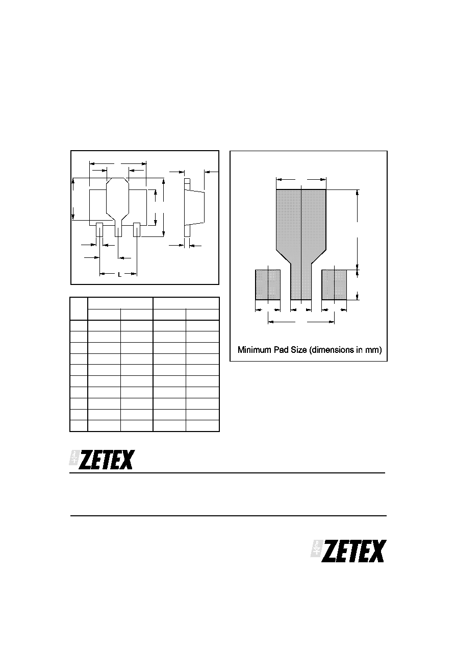
PACKAGE DIMENSIONS
PAD LAYOUT DETAILS
5
Zetex plc.
Fields New Road, Chadderton, Oldham, OL9-8NP, United Kingdom.
Telephone: (44)161 622 4422 (Sales), (44)161 622 4444 (General Enquiries)
Fax: (44)161 622 4420
Zetex GmbH
Zetex Inc.
Zetex (Asia) Ltd.
These are supported by
Streitfeldstraþe 19
Suite 315
3701-04 Metroplaza, Tower 1
agents and distributors in
D-81673 M¸nchen
700 Veterans Memorial Highway Hing Fong Road,
major countries world-wide
Germany
Hauppauge NY 11788
Kwai Fong
© Zetex plc 2001
USA
Hong Kong
Telefon: (49) 89 45 49 49 0
Telephone: (631) 543-7100
Telephone:(852) 26100 611
Fax: (49) 89 45 49 49 49
Fax: (631) 864-7630
Fax: (852) 24250 494
www.zetex.com
This publication is issued to provide outline information only which (unless agreed by the Company in writing) may not be used, applied or reproduced for
any purpose or form part of any order or contract or be regarded as a representation relating to the products or services concerned. The Company reserves
the right to alter without notice the specification, design, price or conditions of supply of any product or service.
1.2
1.0
1.2
3.2
1.5
4.0
2.4
SOT89 pattern.
H
A
D B
K
G
N
F
C
DIM
Millimetres
Inches
Min
Max
Min
Max
A
4.40
4.60
0.173
0.181
B
3.75
4.25
.150
0.167
C
1.40
1.60
0.550
0.630
D
-
2.60
-
0.102
F
0.28
0.45
0.011
0.018
G
0.38
0.55
0.015
0.022
H
1.50
1.80
0.060
0.072
K
2.60
2.85
0.102
0.112
L
2.90
3.10
0.114
0.112
N
1.4
1.60
0.055
0.063